CN114339085A - TOF image sensor pixel structure and ranging system - Google Patents
TOF image sensor pixel structure and ranging systemDownload PDFInfo
- Publication number
- CN114339085A CN114339085ACN202011063269.6ACN202011063269ACN114339085ACN 114339085 ACN114339085 ACN 114339085ACN 202011063269 ACN202011063269 ACN 202011063269ACN 114339085 ACN114339085 ACN 114339085A
- Authority
- CN
- China
- Prior art keywords
- transistor
- control module
- image sensor
- pixel structure
- node
- Prior art date
- Legal status (The legal status is an assumption and is not a legal conclusion. Google has not performed a legal analysis and makes no representation as to the accuracy of the status listed.)
- Granted
Links
Images


Landscapes
- Solid State Image Pick-Up Elements (AREA)
- Transforming Light Signals Into Electric Signals (AREA)
Abstract
Description
Translated fromChinese技术领域technical field
本发明涉及图像传感器技术领域,特别是涉及一种TOF图像传感器像素结构及测距系统。The invention relates to the technical field of image sensors, in particular to a TOF image sensor pixel structure and a ranging system.
背景技术Background technique
图像传感器是组成数字摄像头的重要组成部分,根据元件的不同,图像传感器可以分为CCD(Charge Coupled Device,电荷耦合元件)图像传感器和CMOS(ComplementaryMetal Oxide Semiconductor,互补金属氧化物半导体)图像传感器两大类。而由于CMOS图像传感器具有功耗、成本低、易于标准化生产等优点,在各个领域得到了广泛应用。Image sensor is an important part of digital camera. According to different components, image sensor can be divided into CCD (Charge Coupled Device, Charge Coupled Device) image sensor and CMOS (Complementary Metal Oxide Semiconductor, Complementary Metal Oxide Semiconductor) image sensor. kind. CMOS image sensors have been widely used in various fields due to their advantages of power consumption, low cost, and easy standardized production.
随着三维成像信息技术的迅速发展,特别是建筑测量、室内定位和导航、立体影像和辅助生活环境应用对飞行时间(Time-of-Flight,TOF)成像提出了迫切需求,应用于飞行时间成像系统的CMOS图像传感器像素结构也得了快速的发展。TOF图像传感器可以分为dTOF图像传感器和iTOF图像传感器。其中,dTOF图像传感器,直接测量飞行时间,即测量发射光脉冲与接收光脉冲的时间间隔。其中,iTOF图像传感器,间接测量飞行时间,通常采用一种测相位偏移的方法,即测量发射正弦波/方波与接收正弦波/方波之间的相位差。对于所有类型的TOF图像传感器而言,测距精度是其一项重要参数,测距精度越高,目标的三维图像探测就越准确。With the rapid development of 3D imaging information technology, especially the application of building measurement, indoor positioning and navigation, stereo imaging and assisted living environment, there is an urgent need for Time-of-Flight (TOF) imaging, which is applied to time-of-flight imaging. The system's CMOS image sensor pixel structure has also developed rapidly. TOF image sensors can be classified into dTOF image sensors and iTOF image sensors. Among them, the dTOF image sensor directly measures the time of flight, that is, the time interval between the emitted light pulse and the received light pulse. Among them, the iTOF image sensor, which indirectly measures the flight time, usually adopts a method of measuring phase offset, that is, measuring the phase difference between the transmitted sine/square wave and the received sine/square wave. For all types of TOF image sensors, ranging accuracy is an important parameter. The higher the ranging accuracy, the more accurate the three-dimensional image detection of the target.
而在传统的TOF图像传感器像素中,光电二极管的尺寸过大(例如长度过长)会对电荷的传输时间或传输效率有负面影响,由此也会对测距能力、测距精度带来负面影响。In conventional TOF image sensor pixels, too large photodiode size (for example, too long length) will have a negative impact on the transfer time or transfer efficiency of charges, which will also have a negative impact on ranging capability and ranging accuracy. influences.
针对以上问题,本领域技术人员一直在寻求解决方法。For the above problems, those skilled in the art have been seeking solutions.
前面的叙述在于提供一般的背景信息,并不一定构成现有技术。The preceding statements are intended to provide general background information and may not constitute prior art.
发明内容SUMMARY OF THE INVENTION
本发明要解决的技术问题在于,针对上述现有技术的缺陷,TOF图像传感器像素结构及测距系统,以实现缩短光电二极管产生的电荷的传输时间、提高光电二极管产生的电荷的传输效率的目的,进而能够实现提升测距能力、测距精度的目的。The technical problem to be solved by the present invention is that, in view of the above-mentioned defects of the prior art, the pixel structure of the TOF image sensor and the ranging system can shorten the transfer time of the charges generated by the photodiode and improve the transfer efficiency of the charges generated by the photodiode. , so as to achieve the purpose of improving the ranging capability and the ranging accuracy.
本发明是这样实现的:The present invention is realized in this way:
本发明提供了一种TOF图像传感器像素结构,包括第一读取控制模块、第二读取控制模块及至少两个预设尺寸的小光传感器。第一读取控制模块中包括至少两个第一传输晶体管,且第一读取控制模块通过至少两个第一传输晶体管分别与至少两个预设尺寸的小光传感器一一对应连接。第二读取控制模块中包括至少两个第二传输晶体管,且第二读取控制模块通过至少两个第二传输晶体管分别与至少两个预设尺寸的小光传感器一一对应连接。其中,连接同一个小光传感器的第一传输晶体管和第二传输晶体管对称设置。The present invention provides a pixel structure of a TOF image sensor, which includes a first reading control module, a second reading control module and at least two small light sensors with preset sizes. The first reading control module includes at least two first transmission transistors, and the first reading control module is respectively connected with at least two small light sensors of preset size through the at least two first transmission transistors in a one-to-one correspondence. The second read control module includes at least two second transfer transistors, and the second read control module is respectively connected with at least two small light sensors of preset size through the at least two second transfer transistors in a one-to-one correspondence. Wherein, the first transfer transistor and the second transfer transistor connected to the same small light sensor are arranged symmetrically.
可选地,小光传感器包括光电二极管、光栅或光导体中的一种。Optionally, the small light sensor includes one of a photodiode, a grating, or a photoconductor.
可选地,第一读取控制模块还包括第一复位晶体管、第一双转换增益控制单元、第一存储电容、第一节点及第一输出单元。其中,第一复位晶体管的第一端连接至电压源,第一复位晶体管的第二端通过第一双转换增益控制单元耦接于第一节点。至少两个第一传输晶体管的第一端分别与至少两个预设尺寸的小光传感器的负极一一对应连接,至少两个第一传输晶体管的第二端均连接第一节点。第一存储电容和第一输出单元均与第一节点连接。第二读取控制模块还包括第二复位晶体管、第二双转换增益控制单元、第二存储电容、第二节点及第二输出单元。其中,第二复位晶体管的第一端连接至电压源,第二复位晶体管的第二端通过第二双转换增益控制单元耦接于第二节点。至少两个第二传输晶体管的第一端分别与至少两个预设尺寸的小光传感器的负极一一对应连接,至少两个第二传输晶体管的第二端均连接第二节点。第二存储电容和第二输出单元均与第二节点连接。Optionally, the first read control module further includes a first reset transistor, a first double conversion gain control unit, a first storage capacitor, a first node and a first output unit. The first terminal of the first reset transistor is connected to the voltage source, and the second terminal of the first reset transistor is coupled to the first node through the first double conversion gain control unit. The first ends of the at least two first transfer transistors are respectively connected to the negative poles of the at least two small photosensors with a preset size in a one-to-one correspondence, and the second ends of the at least two first transfer transistors are both connected to the first node. Both the first storage capacitor and the first output unit are connected to the first node. The second read control module further includes a second reset transistor, a second double conversion gain control unit, a second storage capacitor, a second node and a second output unit. The first terminal of the second reset transistor is connected to the voltage source, and the second terminal of the second reset transistor is coupled to the second node through the second double conversion gain control unit. The first ends of the at least two second pass transistors are respectively connected to the negative poles of the at least two small photosensors with a preset size in a one-to-one correspondence, and the second ends of the at least two second pass transistors are both connected to the second node. Both the second storage capacitor and the second output unit are connected to the second node.
可选地,第一输出单元包括第一源极跟随晶体管和第一行选择晶体管,第二输出单元包括第二源极跟随晶体管和第二行选择晶体管。第一源极跟随晶体管的第一控制端连接第一节点,第一源极跟随晶体管的第一端连接电压源,第一源极跟随晶体管的第二端通过第一行选择晶体管连接第一数据输出线。第二源极跟随晶体管的第二控制端连接第二节点,第二源极跟随晶体管的第一端连接电压源,第二源极跟随晶体管的第二端通过第二行选择晶体管连接第二数据输出线。Optionally, the first output unit includes a first source follower transistor and a first row select transistor, and the second output unit includes a second source follower transistor and a second row select transistor. The first control terminal of the first source follower transistor is connected to the first node, the first terminal of the first source follower transistor is connected to the voltage source, and the second terminal of the first source follower transistor is connected to the first data through the first row selection transistor output line. The second control terminal of the second source follower transistor is connected to the second node, the first terminal of the second source follower transistor is connected to the voltage source, and the second terminal of the second source follower transistor is connected to the second data through the second row selection transistor output line.
可选地,第一节点为第一浮动扩散节点,第二节点为第二浮动扩散节点。Optionally, the first node is a first floating diffusion node, and the second node is a second floating diffusion node.
可选地,还包括电荷平衡单元。电荷平衡单元与第一读取控制模块的第一浮动扩散节点和第二读取控制模块的第二浮动扩散节点相连,用于在重置后平衡第一浮动扩散节点和第二浮动扩散节点的电荷。Optionally, a charge balance unit is also included. The charge balancing unit is connected to the first floating diffusion node of the first read control module and the second floating diffusion node of the second read control module, and is used for balancing the first floating diffusion node and the second floating diffusion node after resetting charge.
可选地,第一双转换增益控制单元包括第一双转换增益控制晶体管和第一双转换增益电容。第二双转换增益控制单元包括第二双转换增益控制晶体管和第二双转换增益电容。Optionally, the first double-conversion gain control unit includes a first double-conversion gain control transistor and a first double-conversion gain capacitor. The second double-conversion gain control unit includes a second double-conversion gain control transistor and a second double-conversion gain capacitor.
可选地,第一双转换增益电容和第二双转换增益电容均为寄生电容。Optionally, both the first double conversion gain capacitor and the second double conversion gain capacitor are parasitic capacitors.
可选地,第一存储电容为第一双转换增益电容,第二存储电容为第二双转换增益电容。Optionally, the first storage capacitor is a first double conversion gain capacitor, and the second storage capacitor is a second double conversion gain capacitor.
可选地,包括四个小光传感器,且第一读取控制模块中第一传输晶体管的数量和第二读取控制模块中第二传输晶体管的数量与小光传感器的数量相对应。Optionally, four small light sensors are included, and the number of first transfer transistors in the first read control module and the number of second transfer transistors in the second read control module correspond to the number of small light sensors.
可选地,第一读取控制模块中的第一传输晶体管与第二读取控制模块中的第二传输晶体管在光传感器的曝光过程中交替导通的相位相差π。Optionally, the phases in which the first transfer transistor in the first read control module and the second transfer transistor in the second read control module are alternately turned on during the exposure process of the photosensor are different by π.
可选地,还包括至少两个抗溢出晶体管,且每个抗溢出晶体管对应一个小光传感器。每个抗溢出晶体管的第一端耦接至电压源,每个抗溢出晶体管的第二端连接对应的小光传感器,以在调制光未打开时移除对应的小光传感器因背景光所产生的电荷。Optionally, at least two anti-overflow transistors are also included, and each anti-overflow transistor corresponds to a small light sensor. The first end of each anti-overflow transistor is coupled to the voltage source, and the second end of each anti-overflow transistor is connected to the corresponding small light sensor, so as to remove the corresponding small light sensor caused by the background light when the modulated light is not turned on charge.
可选地,预设尺寸包括以下至少一种:0.5x0.5um、2.5x2.5um、3x3um、4X4 um。Optionally, the preset size includes at least one of the following: 0.5x0.5um, 2.5x2.5um, 3x3um, 4X4um.
可选地,小光传感器的形状包括以下至少一种:矩形,圆形,或轴对称的图形。Optionally, the shape of the small light sensor includes at least one of the following: a rectangle, a circle, or an axisymmetric figure.
可选地,小光传感器的数量范围为2至30。Optionally, the number of small light sensors ranges from 2 to 30.
本发明还提供一种测距系统,包括:图像传感器,图像传感器包括多个排成行和列的像素阵列,每个像素包括如上所描述的TOF图像传感器像素结构。控制信号处理单元,用于控制系统工作过程并处理像素阵列获取的图像数据。可调制光源,用于接收调制信号后产生调制光信号,并将接收到的调制信号反馈至像素阵列。The present invention also provides a ranging system, comprising: an image sensor, the image sensor includes a plurality of pixel arrays arranged in rows and columns, and each pixel includes the TOF image sensor pixel structure as described above. The control signal processing unit is used to control the working process of the system and process the image data obtained by the pixel array. The modulated light source is used for generating a modulated light signal after receiving the modulated signal, and feeding back the received modulated signal to the pixel array.
本发明提供的TOF图像传感器像素结构及测距系统,其中,TOF图像传感器像素结构,包括第一读取控制模块、第二读取控制模块及至少两个预设尺寸的小光传感器。第一读取控制模块中包括至少两个第一传输晶体管,且第一读取控制模块通过至少两个第一传输晶体管分别与至少两个预设尺寸的小光传感器一一对应连接。第二读取控制模块中包括至少两个第二传输晶体管,且第二读取控制模块通过至少两个第二传输晶体管分别与至少两个预设尺寸的小光传感器一一对应连接。其中,连接同一个小光传感器的第一传输晶体管和第二传输晶体管对称设置。因此,本发明通过使用多个小尺寸的小光传感器能够节省所有小光传感器产生的电荷的传输时间、提高所有小光传感器产生的电荷的传输效率,并且对称设置的第一传输晶体管和第二传输晶体管产生的电场,能够在不需要额外的附加驱动电荷传输的电场的前提下,保障每个小光传感器产生的电荷的传输速率,故而,本发明能够提高光生电荷的传输效率,进而能够实现提升测距能力、测距精度的目的。The TOF image sensor pixel structure and ranging system provided by the present invention, wherein the TOF image sensor pixel structure includes a first reading control module, a second reading control module and at least two small light sensors of preset size. The first reading control module includes at least two first transmission transistors, and the first reading control module is respectively connected with at least two small light sensors of preset size through the at least two first transmission transistors in a one-to-one correspondence. The second read control module includes at least two second transfer transistors, and the second read control module is respectively connected with at least two small light sensors of preset size through the at least two second transfer transistors in a one-to-one correspondence. Wherein, the first transfer transistor and the second transfer transistor connected to the same small light sensor are arranged symmetrically. Therefore, the present invention can save the transfer time of the charges generated by all the small photosensors and improve the transfer efficiency of the charges generated by all the small photosensors by using a plurality of small-sized small photosensors, and the symmetrically arranged first transfer transistors and second The electric field generated by the transfer transistor can ensure the transfer rate of the charges generated by each small light sensor without the need for an additional electric field for driving charge transfer. Therefore, the present invention can improve the transfer efficiency of the photogenerated charges, thereby realizing The purpose of improving the ranging capability and ranging accuracy.
为让本发明的上述和其他目的、特征和优点能更明显易懂,下文特举较佳实施例,并配合所附图式,作详细说明如下。In order to make the above-mentioned and other objects, features and advantages of the present invention more obvious and easy to understand, the preferred embodiments are exemplified below, and are described in detail as follows in conjunction with the accompanying drawings.
附图说明Description of drawings
图1是本发明第一实施例提供的TOF图像传感器像素结构的第一电路示意图;1 is a first schematic circuit diagram of a pixel structure of a TOF image sensor provided by a first embodiment of the present invention;
图2是本发明第一实施例提供的TOF图像传感器像素结构的第二电路示意图;2 is a second schematic circuit diagram of the pixel structure of the TOF image sensor provided by the first embodiment of the present invention;
图3是本发明第一实施例提供的TOF图像传感器像素结构的布局示意图;3 is a schematic layout diagram of a pixel structure of a TOF image sensor provided by the first embodiment of the present invention;
图4是本发明第一实施例提供的TOF图像传感器像素结构的第三电路示意图;4 is a third schematic circuit diagram of the pixel structure of the TOF image sensor provided by the first embodiment of the present invention;
图5是本发明第二实施例提供的测距系统的结构示意图。FIG. 5 is a schematic structural diagram of a ranging system provided by a second embodiment of the present invention.
具体实施方式Detailed ways
为了使本发明的目的、技术方案及优点更加清楚明白,以下结合附图及实施例,对本发明进行进一步详细说明。应当理解,所描述的实施例仅仅是本发明一部分实施例,而不是全部的实施例。基于本发明中的实施例,本领域普通技术人员在没有做出创造性劳动前提下所获得的所有其他实施例,都属于本发明保护的范围。In order to make the objectives, technical solutions and advantages of the present invention clearer, the present invention will be further described in detail below with reference to the accompanying drawings and embodiments. It should be understood that the described embodiments are only some, but not all, embodiments of the present invention. Based on the embodiments of the present invention, all other embodiments obtained by those of ordinary skill in the art without creative efforts shall fall within the protection scope of the present invention.
尽管本发明使用第一、第二、第三等术语来描述不同的读取控制模块、传输晶体管、、控制端等,但是这些读取控制模块、传输晶体管、、控制端等并不受这些术语的限制。这些术语仅是用来将一个读取控制模块、传输晶体管、、控制端等与另一个读取控制模块、传输晶体管、、控制端等区分开来。除非另有定义,否则本发明所使用的所有术语(包括技术术语和科学术语)具有与本发明所属领域的普通技术人员所通常理解的意思。Although the present invention uses the terms first, second, third, etc. to describe different read control modules, pass transistors, control terminals, etc., these read control modules, pass transistors, control terminals, etc. are not subject to these terms limits. These terms are only used to distinguish one read control module, pass transistor, control terminal, etc. from another read control module, pass transistor, control terminal, etc. Unless otherwise defined, all terms (including technical and scientific terms) used in the present invention have the same meaning as commonly understood by one of ordinary skill in the art to which this invention belongs.
在发明中,小光传感器可以是用于将可见光转换为电子(或称电荷、光生电荷)的任何感光性结构,例如小光电二极管PD、小光栅或小光导体中的任一者。优选地,本发明中光传感器可以为小光电二极管PD(下文使用小光电二极管PD进行描述)。In the invention, the small light sensor can be any photosensitive structure for converting visible light into electrons (or electric charge, photo-generated charge), such as any of a small photodiode PD, a small grating, or a small photoconductor. Preferably, the light sensor in the present invention may be a small photodiode PD (described below using a small photodiode PD).
下面结合附图对本发明实施例做进一步详述。The embodiments of the present invention will be described in further detail below with reference to the accompanying drawings.
第一实施例:First embodiment:
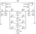
图1是本发明第一实施例提供的TOF图像传感器像素结构的第一电路示意图。为了清楚的描述本发明第一实施例提供的TOF图像传感器像素结构,请参见图1。FIG. 1 is a first schematic circuit diagram of a pixel structure of a TOF image sensor according to a first embodiment of the present invention. For a clear description of the pixel structure of the TOF image sensor provided by the first embodiment of the present invention, please refer to FIG. 1 .
本发明第一实施例提供的TOF图像传感器像素结构,包括第一读取控制模块M1、第二读取控制模块M2及至少两个预设尺寸的小光电二极管PD。The pixel structure of the TOF image sensor provided by the first embodiment of the present invention includes a first reading control module M1, a second reading control module M2, and at least two small photodiodes PD of predetermined sizes.
其中,第一读取控制模块M1中包括至少两个第一传输晶体管MIX1,且第一读取控制模块M1通过至少两个第一传输晶体管MIX1分别与至少两个预设尺寸的小光电二极管PD一一对应连接。其中,第二读取控制模块M2中包括至少两个第二传输晶体管MIX2,且第二读取控制模块M2通过至少两个第二传输晶体管MIX2分别与至少两个预设尺寸的小光电二极管PD一一对应连接。其中,连接同一个小光电二极管PD的第一传输晶体管MIX1和第二传输晶体管MIX2对称设置。Wherein, the first read control module M1 includes at least two first transfer transistors MIX1, and the first read control module M1 connects at least two small photodiodes PD with a preset size through the at least two first transfer transistors MIX1 respectively. One-to-one connection. Wherein, the second reading control module M2 includes at least two second transfer transistors MIX2, and the second reading control module M2 connects at least two small photodiodes PD with a preset size through the at least two second transfer transistors MIX2 respectively. One-to-one connection. Wherein, the first transfer transistor MIX1 and the second transfer transistor MIX2 connected to the same small photodiode PD are symmetrically arranged.
在一实施方式中,第一读取控制模块M1还可以包括第一复位晶体管RST1、第一双转换增益控制单元、第一存储电容C1、第一节点Q1及第一输出单元。其中,第一复位晶体管RST1的第一端连接至电压源VDD,第一复位晶体管RST1的第二端通过第一双转换增益控制单元耦接于第一节点Q1。至少两个第一传输晶体管MIX1的第一端分别与至少两个预设尺寸的小光电二极管PD的负极一一对应连接,至少两个第一传输晶体管MIX1的第二端均连接第一节点Q1。第一存储电容C1和第一输出单元均与第一节点Q1连接。In one embodiment, the first read control module M1 may further include a first reset transistor RST1, a first double conversion gain control unit, a first storage capacitor C1, a first node Q1 and a first output unit. The first terminal of the first reset transistor RST1 is connected to the voltage source VDD, and the second terminal of the first reset transistor RST1 is coupled to the first node Q1 through the first double conversion gain control unit. The first ends of the at least two first pass transistors MIX1 are respectively connected to the negative poles of the at least two small photodiodes PD of a preset size in a one-to-one correspondence, and the second ends of the at least two first pass transistors MIX1 are both connected to the first node Q1 . Both the first storage capacitor C1 and the first output unit are connected to the first node Q1.
在一实施方式中,第一节点Q1可以是为了便于描述而设置的虚拟节点,也可以是实际设置的浮动扩散节点。当第一节点Q1为浮动扩散节点时,可以称为第一浮动扩散节点。In one embodiment, the first node Q1 may be a virtual node set for convenience of description, or may be an actually set floating diffusion node. When the first node Q1 is a floating diffusion node, it may be referred to as a first floating diffusion node.
在一实施方式中,第一读取控制模块M1中的第一复位晶体管RST1可以用于根据复位信号重置电压(例如重置第一浮动扩散节点的电压或重置第一存储电容C1的电压)。In one embodiment, the first reset transistor RST1 in the first read control module M1 can be used to reset the voltage according to a reset signal (eg, reset the voltage of the first floating diffusion node or reset the voltage of the first storage capacitor C1 ). ).
在一实施方式中,第一读取控制模块M1中的第一双转换增益控制单元可以用于实现增益控制和电荷存储。In one embodiment, the first double-conversion gain control unit in the first read control module M1 may be used to implement gain control and charge storage.
在一实施方式中,第一读取控制模块M1中的第一双转换增益控制单元可以包括第一双转换增益控制晶体管DCG1和第一双转换增益电容Cdcg1,第一双转换增益控制晶体管DCG1接于第一复位晶体管RST1的第二端和对应的第一节点Q1之间,第一双转换增益电容Cdcg1的第一端耦接于第一双转换增益控制晶体管DCG1和第一复位晶体管RST1之间,第一双转换增益电容Cdcg1的第二端连接至电压源VDD。In one embodiment, the first double-conversion gain control unit in the first read control module M1 may include a first double-conversion gain control transistor DCG1 and a first double-conversion gain capacitor Cdcg1, and the first double-conversion gain control transistor DCG1 is connected to Between the second end of the first reset transistor RST1 and the corresponding first node Q1, the first end of the first double conversion gain capacitor Cdcg1 is coupled between the first double conversion gain control transistor DCG1 and the first reset transistor RST1 , the second end of the first double conversion gain capacitor Cdcg1 is connected to the voltage source VDD.
在一实施方式中,第一读取控制模块M1中的第一存储电容C1可以作为第一双转换增益电容Cdcg1。In one embodiment, the first storage capacitor C1 in the first read control module M1 can be used as the first double conversion gain capacitor Cdcg1.
在其他实施方式中,第一读取控制模块M1中的第一双转换增益控制单元可以仅为一个第一双转换增益控制晶体管DCG1。In other embodiments, the first double-conversion gain control unit in the first read control module M1 may be only one first double-conversion gain control transistor DCG1.
在其他实施方式中,第一双转换增益电容Cdcg1可以为第一复位晶体管RST1与第一双转换增益控制晶体管DCG1的连接点对地的寄生电容。In other embodiments, the first double-conversion gain capacitor Cdcg1 may be a parasitic capacitance between the connection point of the first reset transistor RST1 and the first double-conversion gain control transistor DCG1 to ground.
在一实施方式中,第一读取控制模块M1中的第一传输晶体管MIX1用于转移小光电二极管PD累计的电荷。In one embodiment, the first transfer transistor MIX1 in the first read control module M1 is used to transfer the charges accumulated by the small photodiode PD.
在一实施方式中,第一读取控制模块M1中的第一输出单元用于对第一节点Q1的电压信号或第一存储电容C1的电信号进行放大输出。In one embodiment, the first output unit in the first read control module M1 is used to amplify and output the voltage signal of the first node Q1 or the electrical signal of the first storage capacitor C1.
在一实施方式中,第一读取控制模块M1中的第一输出单元可以包括第一源极跟随晶体管SF1和第一行选择晶体管RS1。第一源极跟随晶体管SF1的第一控制端连接第一节点Q1,第一源极跟随晶体管SF1的第一端连接电压源VDD,第一源极跟随晶体管SF1的第二端通过第一行选择晶体管RS1连接第一数据输出线BL1In one embodiment, the first output unit in the first read control module M1 may include a first source follower transistor SF1 and a first row select transistor RS1. The first control terminal of the first source follower transistor SF1 is connected to the first node Q1, the first terminal of the first source follower transistor SF1 is connected to the voltage source VDD, and the second terminal of the first source follower transistor SF1 is selected by the first row The transistor RS1 is connected to the first data output line BL1
在一实施方式中,第二读取控制模块M2还包括第二复位晶体管RST2、第二双转换增益控制单元、第二存储电容C2、第二节点Q2及第二输出单元。其中,第二复位晶体管RST2的第一端连接至电压源VDD,第二复位晶体管RST2的第二端通过第二双转换增益控制单元耦接于第二节点Q2。至少两个第二传输晶体管MIX2的第一端分别与至少两个预设尺寸的小光电二极管PD的负极一一对应连接,至少两个第二传输晶体管MIX2的第二端均连接第二节点Q2。第二存储电容C2和第二输出单元均与第二节点Q2连接。In one embodiment, the second read control module M2 further includes a second reset transistor RST2, a second double conversion gain control unit, a second storage capacitor C2, a second node Q2 and a second output unit. The first end of the second reset transistor RST2 is connected to the voltage source VDD, and the second end of the second reset transistor RST2 is coupled to the second node Q2 through the second double conversion gain control unit. The first ends of the at least two second pass transistors MIX2 are respectively connected to the negative poles of the at least two small photodiodes PD with a preset size in a one-to-one correspondence, and the second ends of the at least two second pass transistors MIX2 are both connected to the second node Q2 . Both the second storage capacitor C2 and the second output unit are connected to the second node Q2.
在一实施方式中,第二节点Q2可以是为了便于描述而设置的虚拟节点,也可以是实际设置的浮动扩散节点。当第二节点Q2为浮动扩散节点时,可以称为第二浮动扩散节点。In one embodiment, the second node Q2 may be a virtual node set for convenience of description, or may be an actually set floating diffusion node. When the second node Q2 is a floating diffusion node, it may be referred to as a second floating diffusion node.
在一实施方式中,第二读取控制模块M2中的第二复位晶体管RST2可以用于根据复位控制信号重置电压(例如重置第二浮动扩散节点FD2的电压或重置第二存储电容C2的电压)。In one embodiment, the second reset transistor RST2 in the second read control module M2 may be used to reset the voltage according to the reset control signal (eg, reset the voltage of the second floating diffusion node FD2 or reset the second storage capacitor C2 ) voltage).
在一实施方式中,第二读取控制模块M2中的第二双转换增益控制单元可以用于实现增益控制和电荷存储。In one embodiment, the second double-conversion gain control unit in the second read control module M2 may be used to implement gain control and charge storage.
在一实施方式中,第二读取控制模块M2中的第二双转换增益控制单元可以包括第二双转换增益控制晶体管DCG2和第二双转换增益电容Cdcg2,第二双转换增益控制晶体管DCG2耦接于第二复位晶体管RST2的第二端和对应的第二节点Q2之间,第二双转换增益电容Cdcg2的第二端耦接于第二双转换增益控制晶体管DCG2和第二复位晶体管RST2之间,第二双转换增益电容Cdcg2的第二端连接至电压源VDD。In one embodiment, the second double-conversion gain control unit in the second read control module M2 may include a second double-conversion gain control transistor DCG2 and a second double-conversion gain capacitor Cdcg2, and the second double-conversion gain control transistor DCG2 is coupled to Connected between the second end of the second reset transistor RST2 and the corresponding second node Q2, the second end of the second double conversion gain capacitor Cdcg2 is coupled between the second double conversion gain control transistor DCG2 and the second reset transistor RST2. During this time, the second terminal of the second double conversion gain capacitor Cdcg2 is connected to the voltage source VDD.
在一实施方式中,第二读取控制模块中的第二存储电容可以作为第二双转换增益电容Cdcg2。In one embodiment, the second storage capacitor in the second read control module can be used as the second double conversion gain capacitor Cdcg2.
在其他实施方式中,第二双转换增益电容Cdcg2为第二复位晶体管RST2与第二双转换增益控制晶体管DCG2的连接点对地的寄生电容。In other embodiments, the second double-conversion gain capacitor Cdcg2 is a parasitic capacitance between the connection point of the second reset transistor RST2 and the second double-conversion gain control transistor DCG2 to ground.
在一实施方式中,第二读取控制模块M2中的第二传输晶体管MIX2用于转移小光电二极管PD累计的电荷。In one embodiment, the second transfer transistor MIX2 in the second read control module M2 is used to transfer the charges accumulated by the small photodiode PD.
在一实施方式中,第二读取控制单元M2的第二传输晶体管MIX2与第一读取控制单元M1的第一传输晶体管MIX1在小光电二极管PD的曝光过程中交替导通以交替地将小光电二极管PD累积的电荷分别转移至第二浮动扩散节点FD2(或第一存储电容C1)或第一浮动扩散节点FD1(或第二存储电容C2)。具体地,本实施方式中,通过设置第一读取控制模块M1、第二读取控制模块M2分别与小光电二极管PD耦接,并在小光电二极管PD的曝光过程中控制第一传输晶体管MIX1与第二传输晶体管MIX2交替导通以交替地将小光电二极管PD累积的电荷转移至对应的浮动扩散节点(或存储电容),通过计算第一读取控制模块M1与第二读取控制模块M2对应的浮动扩散节点(或存储电容)积累的有效光信号,可确定光脉冲的飞行时间,从而使得该像素结构可以适用于TOF技术的图像传感器。并且由于第一读取控制模块M1和第二读取控制模块M2采用传输晶体管耦接小光电二极管PD与对应的浮动扩散节点(或存储电容),通过传输晶体管将小光电二极管PD累积的电荷转移至浮动扩散节点(存储电容),使得该像素结构可以支持滚动曝光模式。In one embodiment, the second transfer transistor MIX2 of the second read control unit M2 and the first transfer transistor MIX1 of the first read control unit M1 are alternately turned on during the exposure process of the small photodiode PD to alternately connect the small photodiode PD. The charges accumulated by the photodiode PD are transferred to the second floating diffusion node FD2 (or the first storage capacitor C1 ) or the first floating diffusion node FD1 (or the second storage capacitor C2 ), respectively. Specifically, in this embodiment, the first read control module M1 and the second read control module M2 are respectively coupled to the small photodiode PD, and control the first transfer transistor MIX1 during the exposure process of the small photodiode PD It is alternately turned on with the second transfer transistor MIX2 to alternately transfer the charge accumulated by the small photodiode PD to the corresponding floating diffusion node (or storage capacitor), by calculating the first read control module M1 and the second read control module M2 The effective light signal accumulated by the corresponding floating diffusion node (or storage capacitor) can determine the flight time of the light pulse, so that the pixel structure can be applied to the image sensor of TOF technology. And because the first read control module M1 and the second read control module M2 use transfer transistors to couple the small photodiode PD and the corresponding floating diffusion node (or storage capacitor), the charge accumulated by the small photodiode PD is transferred through the transfer transistor. to the floating diffusion node (storage capacitor), so that the pixel structure can support rolling exposure mode.
在一实施方式中,第二读取控制模块M2中的第二传输晶体管MIX2与第一读取控制模块M1中的第一传输晶体管MIX1在小光电二极管PD的曝光过程中交替导通的相位相差π。In one embodiment, the phase difference between the second transfer transistor MIX2 in the second read control module M2 and the first transfer transistor MIX1 in the first read control module M1 is alternately turned on during the exposure process of the small photodiode PD pi.
在一实施方式中,第二读取控制模块M2中的第二输出单元用于对第二浮动扩散节点FD2或第二存储电容C2的电压信号进行放大输出。In one embodiment, the second output unit in the second read control module M2 is used to amplify and output the voltage signal of the second floating diffusion node FD2 or the second storage capacitor C2.
在一实施方式中,第二读取控制模块M2中的第二输出单元包括第二源极跟随晶体管SF2和第二行选择晶体管RS2。第二源极跟随晶体管SF2的第二控制端连接第二节点,第二源极跟随晶体管SF2的第一端连接电压源VDD,第二源极跟随晶体管SF2的第二端通过第二行选择晶体管RS2连接第二数据输出线BL2。In one embodiment, the second output unit in the second read control module M2 includes a second source follower transistor SF2 and a second row select transistor RS2. The second control terminal of the second source follower transistor SF2 is connected to the second node, the first terminal of the second source follower transistor SF2 is connected to the voltage source VDD, and the second terminal of the second source follower transistor SF2 passes through the second row selection transistor RS2 is connected to the second data output line BL2.
在一实施方式中,第二读取控制模块M2和第一读取控制模块M1可以在本实施例提供的TOF图像传感器像素结构的衬底中对称设置。In one embodiment, the second reading control module M2 and the first reading control module M1 may be symmetrically arranged in the substrate of the pixel structure of the TOF image sensor provided in this embodiment.
图2是本发明第一实施例提供的TOF图像传感器像素结构的第二电路示意图。FIG. 2 is a second schematic circuit diagram of the pixel structure of the TOF image sensor provided by the first embodiment of the present invention.
参见图2,在一实施方式中,本发明第一实施例提供的TOF图像传感器像素结构例如可以包括四个小光电二极管PD,且第一读取控制模块M1中第一传输晶体管的数量MIX1和第二读取控制模块M2中第二传输晶体管MIX2的数量与小小光电二极管PD的数量相对应。具体地,四个小光电二极管PD通过第一读取控制模块M1中的四个第一传输晶体管MIX1和第二读取控制模块M2中的四个第二传输晶体管MIX2形成并联。Referring to FIG. 2 , in one embodiment, the pixel structure of the TOF image sensor provided by the first embodiment of the present invention may include, for example, four small photodiodes PD, and the numbers MIX1 and MIX1 of the first transfer transistors in the first read control module M1 and The number of the second transfer transistors MIX2 in the second read control module M2 corresponds to the number of the small photodiodes PD. Specifically, the four small photodiodes PD are formed in parallel by the four first transfer transistors MIX1 in the first read control module M1 and the four second transfer transistors MIX2 in the second read control module M2.
在一实施方式中,本实施例中至少两个的小光电二极管PD(例如四个小光电二极管PD)可以理解为将传统的大尺寸的光电二极管,拆分为多个小光电二极管PD进行并联。本实施例提供的TOF图像传感器像素结构通过使用多个小尺寸的小光电二极管PD能够节省所有小光电二极管PD产生的电荷的传输时间、提高所有小光电二极管PD产生的电荷的传输效率,并且对称设置的第一传输晶体管MIX1和第二传输晶体管MIX2产生的电场,能够在不需要额外的附加驱动电荷传输的电场的前提下,保障每个小光电二极管PD产生的电荷的传输速率,故而,本实施例提供的TOF图像传感器像素结构能够提高光生电荷的传输效率,进而能够实现提升测距能力、测距精度的目的。In one embodiment, at least two small photodiodes PD (for example, four small photodiodes PD) in this embodiment can be understood as dividing a traditional large-sized photodiode into multiple small photodiodes PD for parallel connection. . The TOF image sensor pixel structure provided by this embodiment can save the transfer time of the charges generated by all the small photodiodes PD, improve the transfer efficiency of the charges generated by all the small photodiodes PD by using a plurality of small photodiodes PD, and is symmetrical The electric field generated by the set first transfer transistor MIX1 and the second transfer transistor MIX2 can ensure the transfer rate of the charges generated by each small photodiode PD without the need for an additional electric field for driving charge transfer. Therefore, this The pixel structure of the TOF image sensor provided by the embodiment can improve the transmission efficiency of photo-generated charges, thereby achieving the purpose of improving the ranging capability and the ranging accuracy.
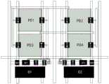
图3是本发明第一实施例提供的TOF图像传感器像素结构的布局示意图。FIG. 3 is a schematic layout diagram of a pixel structure of a TOF image sensor provided by the first embodiment of the present invention.
参见图3,在一实施方式中,本发明第一实施例提供的TOF图像传感器像素结构中的小光电二极管PD、第一读取控制模块M1及读取控制模块M2可以在衬底中对称设置。例如,四个小光电二极管PD在衬底中对称设置,第一读取控制模块M1中的第一传输晶体管MIX1、第一复位晶体管RST1、第一双转换增益控制晶体管DCG1、第一源极跟随晶体管SF1及第一行选择晶体管RS1等等,与第二读取控制模块M2中的第二传输晶体管MIX2、第二复位晶体管RST2、第二双转换增益控制晶体管DCG2、第二源极跟随晶体管SF2及第二行选择晶体管RS2等等在衬底中对称设置。Referring to FIG. 3 , in one embodiment, the small photodiode PD, the first read control module M1 and the read control module M2 in the pixel structure of the TOF image sensor provided by the first embodiment of the present invention may be symmetrically arranged in the substrate . For example, four small photodiodes PD are symmetrically arranged in the substrate, the first transfer transistor MIX1, the first reset transistor RST1, the first double conversion gain control transistor DCG1, the first source follower in the first read control module M1 The transistor SF1 and the first row selection transistor RS1, etc., and the second transfer transistor MIX2, the second reset transistor RST2, the second double conversion gain control transistor DCG2, the second source follower transistor SF2 in the second read control module M2 And the second row selection transistor RS2 and so on are arranged symmetrically in the substrate.
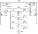
图4是本发明第一实施例提供的TOF图像传感器像素结构的第三电路示意图。FIG. 4 is a third schematic circuit diagram of the pixel structure of the TOF image sensor provided by the first embodiment of the present invention.
参见图4,在一实施方式中,本发明第一实施例提供的TOF图像传感器像素结构还可以包括电荷平衡单元EQ。电荷平衡单元EQ可以与第一读取控制模块M1的第一浮动扩散节点FD1和第二读取控制模块M2的第二浮动扩散节点FD2相连,用于在重置后平衡第一浮动扩散节点FD1和第二浮动扩散节点FD2的电荷。因此,本实施例能够确保TOF图像传感器像素中的几个浮动扩散节点的电压在重置后相等,从而提高图像传感器的测距精度。Referring to FIG. 4 , in one embodiment, the pixel structure of the TOF image sensor provided by the first embodiment of the present invention may further include a charge balance unit EQ. The charge balancing unit EQ may be connected to the first floating diffusion node FD1 of the first read control module M1 and the second floating diffusion node FD2 of the second read control module M2 for balancing the first floating diffusion node FD1 after reset and the charge of the second floating diffusion node FD2. Therefore, the present embodiment can ensure that the voltages of several floating diffusion nodes in the pixels of the TOF image sensor are equal after reset, thereby improving the ranging accuracy of the image sensor.
在其他实施方式中,电荷平衡单元EQ可以与第一读取控制模块M1的第一节点Q1和第二读取控制模块M2的第二节点Q2相连,用于在重置后平衡第一存储电容C1和第二存储电容C2的电荷。因此,本实施例能够确保TOF图像传感器像素中的几个存储电容的电压在重置后相等,从而提高图像传感器的测距精度。In other embodiments, the charge balancing unit EQ may be connected to the first node Q1 of the first read control module M1 and the second node Q2 of the second read control module M2 for balancing the first storage capacitor after resetting C1 and the charge of the second storage capacitor C2. Therefore, the present embodiment can ensure that the voltages of several storage capacitors in the pixels of the TOF image sensor are equal after reset, thereby improving the ranging accuracy of the image sensor.
此外,在一实施方式中,本发明第一实施例提供的TOF图像传感器像素结构还可以包括至少两个抗溢出晶体管(图中均为示出),且每个抗溢出晶体管对应一个小小光电二极管PD。每个抗溢出晶体管的第一端耦接至电压源VDD,每个抗溢出晶体管的第二端连接对应的小小光电二极管PD,以在调制光未打开时移除对应的小小光电二极管PD因背景光所产生的电荷。具体地,在调制光没打开的时候,抗溢出晶体管打开以将不要的背景光信号消除,避免背景光电荷传输到浮动扩散节点,从而抑制背景光,从而能够提高测距精度。In addition, in one embodiment, the pixel structure of the TOF image sensor provided by the first embodiment of the present invention may further include at least two anti-overflow transistors (both shown in the figure), and each anti-overflow transistor corresponds to a small photoelectric diode PD. The first end of each anti-overflow transistor is coupled to the voltage source VDD, and the second end of each anti-overflow transistor is connected to the corresponding small photodiode PD, so as to remove the corresponding small photodiode PD when the modulated light is not turned on Charge due to background light. Specifically, when the modulated light is not turned on, the anti-overflow transistor is turned on to eliminate the unwanted background light signal and prevent the background light charge from being transferred to the floating diffusion node, thereby suppressing the background light, thereby improving the ranging accuracy.
在一实施方式中,小光电二极管PD的预设尺寸可以包括以下至少一种:0.5x0.5um、2.5x2.5um、3x3um、4X4 um。In one embodiment, the predetermined size of the small photodiode PD may include at least one of the following: 0.5x0.5um, 2.5x2.5um, 3x3um, 4x4um.
在一实施方式中,小光电二极管PD的形状可以包括以下至少一种:矩形,圆形,或轴对称的图形(例如轴对称的多边形)。In one embodiment, the shape of the small photodiode PD may include at least one of the following: a rectangle, a circle, or an axisymmetric figure (eg, an axisymmetric polygon).
在一实施方式中,小光电二极管PD的数量范围可以为2至30个。In one embodiment, the number of small photodiodes PD may range from 2 to 30.
本发明第一实施例提供的TOF图像传感器像素结构,包括第一读取控制模块M1、第二读取控制模块M2及至少两个预设尺寸的小光电二极管PD。其中,第一读取控制模块M1中包括至少两个第一传输晶体管MIX1,且第一读取控制模块M1通过至少两个第一传输晶体管MIX1分别与至少两个预设尺寸的小光电二极管PD一一对应连接。其中,第二读取控制模块M2中包括至少两个第二传输晶体管MIX2,且第二读取控制模块M2通过至少两个第二传输晶体管MIX2分别与至少两个预设尺寸的小光电二极管PD一一对应连接。其中,连接同一个小光电二极管PD的第一传输晶体管MIX1和第二传输晶体管MIX2对称设置。因此,本发明第一实施例提供的TOF图像传感器像素结构通过使用多个小尺寸的小光电二极管PD能够节省所有小光电二极管PD产生的电荷的传输时间、提高所有小光电二极管PD产生的电荷的传输效率,并且对称设置的第一传输晶体管MIX1和第二传输晶体管MIX2产生的电场,能够在不需要额外的附加驱动电荷传输的电场的前提下,保障每个小光电二极管PD产生的电荷的传输速率,故而,本发明第一实施例提供的TOF图像传感器像素结构能够提高光生电荷的传输效率,进而能够实现提升测距能力、测距精度的目的。The pixel structure of the TOF image sensor provided by the first embodiment of the present invention includes a first reading control module M1, a second reading control module M2, and at least two small photodiodes PD of predetermined sizes. Wherein, the first read control module M1 includes at least two first transfer transistors MIX1, and the first read control module M1 connects at least two small photodiodes PD with a preset size through the at least two first transfer transistors MIX1 respectively. One-to-one connection. Wherein, the second reading control module M2 includes at least two second transfer transistors MIX2, and the second reading control module M2 connects at least two small photodiodes PD with a preset size through the at least two second transfer transistors MIX2 respectively. One-to-one connection. Wherein, the first transfer transistor MIX1 and the second transfer transistor MIX2 connected to the same small photodiode PD are symmetrically arranged. Therefore, the pixel structure of the TOF image sensor provided by the first embodiment of the present invention can save the transfer time of the charges generated by all the small photodiodes PD by using a plurality of small photodiodes PD, and improve the transmission time of the charges generated by all the small photodiodes PD. The transmission efficiency, and the electric field generated by the symmetrically arranged first transmission transistor MIX1 and second transmission transistor MIX2 can ensure the transmission of the charges generated by each small photodiode PD without the need for an additional electric field for driving charge transmission. Therefore, the pixel structure of the TOF image sensor provided by the first embodiment of the present invention can improve the transmission efficiency of photo-generated charges, thereby achieving the purpose of improving the ranging capability and the ranging accuracy.
第二实施例:Second embodiment:
图5是本发明第二实施例提供的测距系统的结构示意图。为了清楚的描述本发明第二实施例提供的测距系统,请参见图5。FIG. 5 is a schematic structural diagram of a ranging system provided by a second embodiment of the present invention. For a clear description of the ranging system provided by the second embodiment of the present invention, please refer to FIG. 5 .
本发明第二实施例提供的测距系统,包括:图像传感器10、控制信号处理单元11和可调制光源12。The ranging system provided by the second embodiment of the present invention includes: an
其中,图像传感器10包括多个排成行和列的像素阵列,每个像素包括如第一实施例所描述的TOF图像传感器像素结构。The
其中,控制信号处理单元11用于控制系统工作过程并处理所述像素阵列获取的图像数据。Wherein, the control
其中,可调制光源12用于接收调制信号后产生调制光信号,并将接收到的调制信号反馈至所述像素阵列。The modulated
本发明第二实施例提供的测距系统,其图像传感器的TOF图像传感器像素结构至少包括第一读取控制模块M1、第二读取控制模块M2及至少两个预设尺寸的小光电二极管PD。其中,第一读取控制模块M1中包括至少两个第一传输晶体管MIX1,且第一读取控制模块M1通过至少两个第一传输晶体管MIX1分别与至少两个预设尺寸的小光电二极管PD一一对应连接。其中,第二读取控制模块M2中包括至少两个第二传输晶体管MIX2,且第二读取控制模块M2通过至少两个第二传输晶体管MIX2分别与至少两个预设尺寸的小光电二极管PD一一对应连接。其中,连接同一个小光电二极管PD的第一传输晶体管MIX1和第二传输晶体管MIX2对称设置。因此,本发明第二实施例提供的测距系统能够提高光生电荷的传输效率,进而能够实现提升测距能力、测距精度的目的。In the ranging system provided by the second embodiment of the present invention, the TOF image sensor pixel structure of the image sensor includes at least a first reading control module M1, a second reading control module M2 and at least two small photodiodes PD of preset sizes . Wherein, the first read control module M1 includes at least two first transfer transistors MIX1, and the first read control module M1 connects at least two small photodiodes PD with a preset size through the at least two first transfer transistors MIX1 respectively. One-to-one connection. Wherein, the second reading control module M2 includes at least two second transfer transistors MIX2, and the second reading control module M2 connects at least two small photodiodes PD with a preset size through the at least two second transfer transistors MIX2 respectively. One-to-one connection. Wherein, the first transfer transistor MIX1 and the second transfer transistor MIX2 connected to the same small photodiode PD are symmetrically arranged. Therefore, the ranging system provided by the second embodiment of the present invention can improve the transmission efficiency of the photo-generated charges, thereby achieving the purpose of improving the ranging capability and the ranging accuracy.
以上所述实施例的各技术特征可以进行任意的组合,为使描述简洁,未对上述实施例中的各个技术特征所有可能的组合都进行描述,然而,只要这些技术特征的组合不存在矛盾,都应当认为是本说明书记载的范围。The technical features of the above-described embodiments can be combined arbitrarily. For the sake of brevity, all possible combinations of the technical features in the above-described embodiments are not described. However, as long as there is no contradiction between the combinations of these technical features, All should be regarded as the scope described in this specification.
需要说明的是,在本文中,术语“包括”、“包含”或者其任何其他变体意在涵盖非排他性的包含,从而使得包括一系列要素的过程、方法、物品、元件或者装置不仅包括那些要素,而且还包括没有明确列出的其他要素,或者是还包括为这种过程、方法、物品、元件或者装置所固有的要素。在没有更多限制的情况下,由语句“包括一个……”限定的要素,并不排除在包括该要素的过程、方法、物品、元件或者装置中还存在另外的相同要素,此外,本申请不同实施例中具有同样命名的部件、特征、要素可能具有相同含义,也可能具有不同含义,其具体含义需以其在该具体实施例中的解释或者进一步结合该具体实施例中上下文进行确定。It should be noted that, herein, the terms "comprising", "comprising" or any other variation thereof are intended to encompass non-exclusive inclusion, such that a process, method, article, element or device comprising a series of elements includes not only those elements, but also other elements not expressly listed or inherent to such a process, method, article, element or apparatus. Without further limitation, an element defined by the phrase "comprising a..." does not preclude the presence of additional identical elements in the process, method, article, element, or device that includes the element, furthermore, the present application Components, features, and elements with the same names in different embodiments may have the same meaning or may have different meanings, and their specific meanings need to be determined by their explanations in the specific embodiment or further combined with the context in the specific embodiment.
应当理解,尽管在本文可能采用术语第一、第二、第三等来描述各种信息,但这些信息不应限于这些术语。这些术语仅用来将同一类型的信息彼此区分开。取决于语境,如在此所使用的词语"如果"可以被解释成为"在……时"或"当……时"或"响应于确定"。再者,如同在本文中所使用的,单数形式“一”、“一个”和“该”旨在也包括复数形式,除非上下文中有相反的指示。应当进一步理解,术语“包含”、“包括”表明存在所述的特征、步骤、操作、元件、组件、项目、种类、和/或组,但不排除一个或多个其他特征、步骤、操作、元件、组件、项目、种类、和/或组的存在、出现或添加。此处使用的术语“或”和“和/或”被解释为包括性的,或意味着任一个或任何组合。因此,“A、B或C”或者“A、B和/或C”意味着“以下任一个:A;B;C;A和B;A和C;B和C;A、B和C”。仅当元件、功能、步骤或操作的组合在某些方式下内在地互相排斥时,才会出现该定义的例外。It should be understood that although the terms first, second, third, etc. may be used herein to describe various information, such information should not be limited by these terms. These terms are only used to distinguish the same type of information from each other. The word "if" as used herein can be interpreted as "at the time of" or "when" or "in response to determining", depending on the context. Also, as used herein, the singular forms "a," "an," and "the" are intended to include the plural forms as well, unless the context dictates otherwise. It should be further understood that the terms "comprising" and "comprising" indicate the presence of stated features, steps, operations, elements, components, items, kinds, and/or groups, but do not exclude one or more other features, steps, operations, The existence, appearance or addition of an element, component, item, category, and/or group. The terms "or" and "and/or" as used herein are to be construed to be inclusive or to mean any one or any combination. Thus, "A, B or C" or "A, B and/or C" means "any of the following: A; B; C; A and B; A and C; B and C; A, B and C" . Exceptions to this definition arise only when combinations of elements, functions, steps, or operations are inherently mutually exclusive in some way.
以上仅为本申请的较佳实施例而已,并不用以限制本申请,凡在本申请的精神和原则之内所作的任何修改、等同替换或改进等,均应包含在本申请的保护范围之内。The above are only preferred embodiments of the present application, and are not intended to limit the present application. Any modifications, equivalent replacements or improvements made within the spirit and principles of the present application shall be included in the protection scope of the present application. Inside.
Claims (16)
Priority Applications (1)
| Application Number | Priority Date | Filing Date | Title |
|---|---|---|---|
| CN202011063269.6ACN114339085B (en) | 2020-09-30 | 2020-09-30 | TOF image sensor pixel structure and ranging system |
Applications Claiming Priority (1)
| Application Number | Priority Date | Filing Date | Title |
|---|---|---|---|
| CN202011063269.6ACN114339085B (en) | 2020-09-30 | 2020-09-30 | TOF image sensor pixel structure and ranging system |
Publications (2)
| Publication Number | Publication Date |
|---|---|
| CN114339085Atrue CN114339085A (en) | 2022-04-12 |
| CN114339085B CN114339085B (en) | 2025-03-18 |
Family
ID=81031662
Family Applications (1)
| Application Number | Title | Priority Date | Filing Date |
|---|---|---|---|
| CN202011063269.6AActiveCN114339085B (en) | 2020-09-30 | 2020-09-30 | TOF image sensor pixel structure and ranging system |
Country Status (1)
| Country | Link |
|---|---|
| CN (1) | CN114339085B (en) |
Citations (13)
| Publication number | Priority date | Publication date | Assignee | Title |
|---|---|---|---|---|
| CN1828919A (en)* | 2005-02-07 | 2006-09-06 | 三星电子株式会社 | sensor array |
| US20080151091A1 (en)* | 2006-12-22 | 2008-06-26 | Magnachip Semiconductor, Ltd. | Small size, high gain, and low noise pixel for CMOS image sensors |
| KR20120122165A (en)* | 2011-04-28 | 2012-11-07 | 클레어픽셀 주식회사 | Image sensor with wide dynamic range and pixel circuit and operating method thereof |
| US20140078368A1 (en)* | 2012-09-20 | 2014-03-20 | Aptina Imaging Corporation | Triple conversion gain image sensor pixels |
| WO2015113407A1 (en)* | 2014-01-30 | 2015-08-06 | Shanghai Integrated Circuit Research And Development Center Co., Ltd. | Image sensor and data tranmission method thereof |
| CN106068562A (en)* | 2014-03-26 | 2016-11-02 | 索尼公司 | Solid imaging element and imaging device |
| CN108282626A (en)* | 2018-03-01 | 2018-07-13 | 上海晔芯电子科技有限公司 | TOF image sensor pixel structures and TOF imaging systems |
| CN108462841A (en)* | 2018-03-21 | 2018-08-28 | 上海晔芯电子科技有限公司 | Pel array and imaging sensor |
| CN109786403A (en)* | 2017-11-13 | 2019-05-21 | 爱思开海力士有限公司 | Imaging sensor |
| US20190191109A1 (en)* | 2017-12-19 | 2019-06-20 | SmartSens Technology (US) Inc. | Pixel unit with a design for half row reading, an imaging apparatus including the same, and an imaging method thereof |
| CN110034147A (en)* | 2019-03-25 | 2019-07-19 | 思特威(上海)电子科技有限公司 | Imaging sensor with back-to-back layout designs structure |
| CN110557582A (en)* | 2018-06-19 | 2019-12-10 | 思特威(上海)电子科技有限公司 | 3D imaging image sensor pixel circuit based on TOF and ranging system |
| CN212727186U (en)* | 2020-09-30 | 2021-03-16 | 思特威(上海)电子科技股份有限公司 | TOF image sensor pixel structure and ranging system |
- 2020
- 2020-09-30CNCN202011063269.6Apatent/CN114339085B/enactiveActive
Patent Citations (13)
| Publication number | Priority date | Publication date | Assignee | Title |
|---|---|---|---|---|
| CN1828919A (en)* | 2005-02-07 | 2006-09-06 | 三星电子株式会社 | sensor array |
| US20080151091A1 (en)* | 2006-12-22 | 2008-06-26 | Magnachip Semiconductor, Ltd. | Small size, high gain, and low noise pixel for CMOS image sensors |
| KR20120122165A (en)* | 2011-04-28 | 2012-11-07 | 클레어픽셀 주식회사 | Image sensor with wide dynamic range and pixel circuit and operating method thereof |
| US20140078368A1 (en)* | 2012-09-20 | 2014-03-20 | Aptina Imaging Corporation | Triple conversion gain image sensor pixels |
| WO2015113407A1 (en)* | 2014-01-30 | 2015-08-06 | Shanghai Integrated Circuit Research And Development Center Co., Ltd. | Image sensor and data tranmission method thereof |
| CN106068562A (en)* | 2014-03-26 | 2016-11-02 | 索尼公司 | Solid imaging element and imaging device |
| CN109786403A (en)* | 2017-11-13 | 2019-05-21 | 爱思开海力士有限公司 | Imaging sensor |
| US20190191109A1 (en)* | 2017-12-19 | 2019-06-20 | SmartSens Technology (US) Inc. | Pixel unit with a design for half row reading, an imaging apparatus including the same, and an imaging method thereof |
| CN108282626A (en)* | 2018-03-01 | 2018-07-13 | 上海晔芯电子科技有限公司 | TOF image sensor pixel structures and TOF imaging systems |
| CN108462841A (en)* | 2018-03-21 | 2018-08-28 | 上海晔芯电子科技有限公司 | Pel array and imaging sensor |
| CN110557582A (en)* | 2018-06-19 | 2019-12-10 | 思特威(上海)电子科技有限公司 | 3D imaging image sensor pixel circuit based on TOF and ranging system |
| CN110034147A (en)* | 2019-03-25 | 2019-07-19 | 思特威(上海)电子科技有限公司 | Imaging sensor with back-to-back layout designs structure |
| CN212727186U (en)* | 2020-09-30 | 2021-03-16 | 思特威(上海)电子科技股份有限公司 | TOF image sensor pixel structure and ranging system |
Also Published As
| Publication number | Publication date |
|---|---|
| CN114339085B (en) | 2025-03-18 |
Similar Documents
| Publication | Publication Date | Title |
|---|---|---|
| CN212752432U (en) | TOF image sensor pixel structure and ranging system | |
| CN113658967B (en) | Light detection device | |
| TWI524762B (en) | Shared flight time pixel | |
| CN108282626B (en) | TOF image sensor pixel structure and TOF imaging system | |
| KR101751090B1 (en) | Range image sensor | |
| US9229096B2 (en) | Time-of-flight imaging systems | |
| KR101348522B1 (en) | Solid state imaging device and distance image measurement device | |
| CN107247269B (en) | Detection device, pixel unit and array for collecting and processing laser signals | |
| WO2019036237A1 (en) | Detection circuit for photo sensor with stacked substrates | |
| CN107300705B (en) | Lidar ranging system and ranging method based on carrier modulation | |
| CN102447848B (en) | Global shutter pixel unit of complementary metal oxide semiconductor (CMOS) image sensor | |
| CN110557582B (en) | 3D imaging image sensor pixel circuit based on TOF and ranging system | |
| US20140253758A1 (en) | Method and Apparatus for a Time-of-Flight Sensor with Charge Storage | |
| CN114914324B (en) | Single Photon Avalanche Diode | |
| CN212727186U (en) | TOF image sensor pixel structure and ranging system | |
| Hsu et al. | A CMOS time-of-flight depth image sensor with in-pixel background light cancellation and phase shifting readout technique | |
| CN107329133A (en) | Rectifiable imaging laser radar receiver and signal processing method | |
| CN111048540A (en) | Gated pixel unit and 3D image sensor | |
| CN109643523B (en) | Pixel circuit and image sensing system | |
| CN114339085A (en) | TOF image sensor pixel structure and ranging system | |
| CN212677262U (en) | TOF image sensor pixel structure and ranging system | |
| CN212727187U (en) | TOF image sensor pixel structure and ranging system | |
| CN110214444B (en) | Back Illuminated Global Shutter Imaging Array | |
| CN115308756A (en) | A pixel circuit, image sensor and detection device | |
| US20210063588A1 (en) | Imaging devices with capacitively coupled single-photon avalanche diodes |
Legal Events
| Date | Code | Title | Description |
|---|---|---|---|
| PB01 | Publication | ||
| PB01 | Publication | ||
| SE01 | Entry into force of request for substantive examination | ||
| SE01 | Entry into force of request for substantive examination | ||
| GR01 | Patent grant | ||
| GR01 | Patent grant |