CN114336275B - Manufacturing method of electrode contact window and preparation method of semiconductor device - Google Patents
Manufacturing method of electrode contact window and preparation method of semiconductor deviceDownload PDFInfo
- Publication number
- CN114336275B CN114336275BCN202210249550.1ACN202210249550ACN114336275BCN 114336275 BCN114336275 BCN 114336275BCN 202210249550 ACN202210249550 ACN 202210249550ACN 114336275 BCN114336275 BCN 114336275B
- Authority
- CN
- China
- Prior art keywords
- region
- electrode contact
- convex shape
- ridge waveguide
- contact window
- Prior art date
- Legal status (The legal status is an assumption and is not a legal conclusion. Google has not performed a legal analysis and makes no representation as to the accuracy of the status listed.)
- Active
Links
Images


Landscapes
- Drying Of Semiconductors (AREA)
- Optical Modulation, Optical Deflection, Nonlinear Optics, Optical Demodulation, Optical Logic Elements (AREA)
Abstract
Translated fromChinese
Description
Translated fromChinese技术领域technical field
本发明涉及半导体加工技术领域,尤其是涉及一种电极接触窗口的制作方法及半导体器件的制备方法。The invention relates to the technical field of semiconductor processing, in particular to a method for manufacturing an electrode contact window and a method for manufacturing a semiconductor device.
背景技术Background technique
半导体器件是导电性介于良导电体与绝缘体之间,利用半导体材料特殊电特性来完成特定功能的电子器件,可用来产生、控制、接收、变换、放大信号和进行能量转换。A semiconductor device is an electronic device whose conductivity is between a good conductor and an insulator. It uses the special electrical properties of semiconductor materials to complete specific functions. It can be used to generate, control, receive, transform, amplify signals and perform energy conversion.
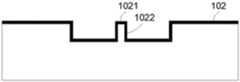
基于脊波导的半导体器件的电流注入位置为脊波导的顶部表面,也称作电极接触窗口,电极接触窗口的顶部表面用来制作金属电极,在这类半导体器件的设计和制作中,对金属电极的尺寸、位置及厚度是有严格要求的,因此,电极接触窗口的制作是非常关键的一步。The current injection position of the semiconductor device based on the ridge waveguide is the top surface of the ridge waveguide, also called the electrode contact window. The top surface of the electrode contact window is used to make the metal electrode. In the design and manufacture of this type of semiconductor device, the metal electrode There are strict requirements on the size, position and thickness of the electrode contact window. Therefore, the fabrication of the electrode contact window is a very critical step.
常规的脊波导上电极窗口的制备方法是在已刻蚀的脊波导及其两侧结构表面生长一层电介质层作为绝缘层,在绝缘层上旋涂光刻胶,利用掩模版对脊波导上方光刻胶进行曝光,确保脊波导顶部表面的绝缘层外露,而脊波导顶部表面以外的其它部位的光刻胶全部保留,之后利用光刻胶做掩模对电介质层进行去除,形成电极接触窗口。The conventional preparation method of the upper electrode window of the ridge waveguide is to grow a layer of dielectric layer on the surface of the etched ridge waveguide and its two side structures as an insulating layer, spin-coat photoresist on the insulating layer, and use a mask to align the upper surface of the ridge waveguide. The photoresist is exposed to ensure that the insulating layer on the top surface of the ridge waveguide is exposed, while the photoresist on other parts other than the top surface of the ridge waveguide is completely reserved, and then the dielectric layer is removed by using the photoresist as a mask to form an electrode contact window .
上述方法要求光刻具有较高的对准精度,且光刻后脊波导两侧的光刻胶会有一定程度的脱落现象,导致其对脊波导侧壁绝缘层保护性差,刻蚀去除脊波导上绝缘层时,使脊波导两侧绝缘层受损,影响电极开窗效果。The above method requires photolithography to have high alignment accuracy, and after photolithography, the photoresist on both sides of the ridge waveguide will fall off to a certain extent, resulting in poor protection for the insulating layer on the side wall of the ridge waveguide, and the removal of the ridge waveguide by etching When the insulating layer is applied, the insulating layers on both sides of the ridge waveguide will be damaged, which will affect the window opening effect of the electrodes.
发明内容Contents of the invention
本发明的目的在于提供一种电极接触窗口的制作方法及半导体器件的制备方法,以缓解现有技术中存在的在形成半导体器件的电极接触窗口的过程中,要求光刻具有较高的对准精度,且光刻后脊波导两侧的光刻胶容易存在一定程度的脱落现象,导致其对脊波导侧壁绝缘层保护性差的技术问题。The object of the present invention is to provide a method for making an electrode contact window and a method for preparing a semiconductor device, so as to relieve the existing technology in the process of forming the electrode contact window of a semiconductor device, which requires photolithography to have a higher alignment. Precision, and the photoresist on both sides of the ridge waveguide is prone to fall off to a certain extent after photolithography, resulting in the technical problem of poor protection for the insulating layer on the side wall of the ridge waveguide.
第一方面,本发明实施例提供的一种电极接触窗口的制作方法,所述电极接触窗口的制作方法包括以下步骤:In the first aspect, an embodiment of the present invention provides a method for manufacturing an electrode contact window, the method for manufacturing an electrode contact window includes the following steps:
步骤S1.提供一具有脊波导的基材,所述脊波导的两侧分别具有凹陷,所述脊波导和所述凹陷的表面均沉积有电介质层,在所述电介质层的表面形成光阻材料层;其中,所述电介质层覆盖在所述脊波导顶部的部分形成上侧结构,所述电介质层覆盖在所述脊波导横向侧壁的部分形成侧部结构;Step S1. Provide a substrate with a ridge waveguide, with depressions on both sides of the ridge waveguide, a dielectric layer is deposited on the surface of the ridge waveguide and the depression, and a photoresist material is formed on the surface of the dielectric layer layer; wherein, the part of the dielectric layer covering the top of the ridge waveguide forms an upper structure, and the dielectric layer covers a part of the lateral sidewall of the ridge waveguide to form a side structure;
步骤S2.所述脊波导与所述凹陷沿横向排布设置;Step S2. The ridge waveguide and the depression are arranged in a transverse direction;
在所述光阻材料层的上方设置掩模版,所述掩模版上具有透光结构,所述透光结构包括第一区域,所述第一区域的横向两侧分别连接有由内向外依次连接的第二区域和第三区域;所述第二区域的透光率分别小于所述第一区域和第三区域的透光率;A reticle is provided above the photoresist material layer, and the reticle has a light-transmitting structure, the light-transmitting structure includes a first region, and the lateral sides of the first region are respectively connected with The second area and the third area; the light transmittance of the second area is less than the light transmittance of the first area and the third area;
所述第一区域位于所述脊波导的上方,且所述第一区域的横向上的两边沿在所述基材上的投影分别位于所述脊波导的两侧;所述第二区域在所述基材上的投影落在所述凹陷内;通过上述掩模版对所述光阻材料层进行曝光;The first region is located above the ridge waveguide, and the projections of the lateral edges of the first region on the substrate are respectively located on both sides of the ridge waveguide; the second region is on the ridge waveguide. The projection on the base material falls in the depression; the photoresist material layer is exposed through the mask plate;
步骤S3.对曝光后的光阻材料层进行显影处理,以使覆盖在所述上侧结构上表面的光阻材料层全部去除,并使位于所述第二区域的正下方的光阻材料层形成上凸形态;Step S3. Developing the exposed photoresist material layer, so that the photoresist material layer covering the upper surface of the upper structure is completely removed, and the photoresist material layer located directly below the second region form a convex shape;
步骤S4.对所述上凸形态进行热处理,所述上凸形态自球化,以形成球冠形态,所述球冠形态横向上靠近所述脊波导的边沿位于所述上侧结构的上表面的边沿处;Step S4. performing heat treatment on the convex shape, the convex shape is self-spheroidized to form a spherical cap shape, and the edge of the spherical cap shape laterally close to the ridge waveguide is located on the upper surface of the upper structure at the edge of
步骤S5.以步骤S4获得的光阻材料层为掩模对所述电介质层进行刻蚀,将上侧结构去除,以形成电极接触窗口。Step S5. Using the photoresist material layer obtained in step S4 as a mask to etch the dielectric layer to remove the upper structure to form an electrode contact window.
进一步的,在步骤S2中,所述第一区域由贯穿所述掩模版的通孔形成;Further, in step S2, the first region is formed by a through hole penetrating through the mask;
和/或,所述第三区域由贯穿所述掩模版的通孔形成。And/or, the third region is formed by a through hole penetrating through the mask.
进一步的,在步骤S2中,所述第二区域的数量为多个,沿横向,所述第一区域和第三区域之间的相邻两个第二区域间隔设置,且间隔的两个第二区域之间区域的透光率大于所述第二区域的透光率。Further, in step S2, the number of the second regions is multiple, and along the lateral direction, two adjacent second regions between the first region and the third region are arranged at intervals, and the interval between two second regions is The light transmittance of the area between the two areas is greater than the light transmittance of the second area.
进一步的,所述第一区域和第三区域之间任意相邻两个所述第二区域中,远离所述第一区域的第二区域的透光率小于等于靠近所述第一区域的第二区域的透光率。Further, among any two adjacent second regions between the first region and the third region, the light transmittance of the second region far away from the first region is less than or equal to that of the second region close to the first region. The light transmittance of the second area.
进一步的,所述上凸形态的高度H与所述上凸形态的宽度D的比值的取值范围为2~6。Further, the ratio of the height H of the convex shape to the width D of the convex shape ranges from 2 to 6.
进一步的,最靠近所述脊波导的上凸形态的上表面与所述上侧结构的上表面之间的垂直距离H1为0.5-1.5微米。Further, the vertical distance H1 between the upper surface of the convex shape closest to the ridge waveguide and the upper surface of the upper structure is 0.5-1.5 microns.
进一步的,最靠近所述脊波导的所述上凸形态与所述侧部结构之间的横向水平距离D1为0.1-0.2微米。Further, the lateral horizontal distance D1 between the convex shape closest to the ridge waveguide and the side structure is 0.1-0.2 microns.
进一步的,在步骤S4中,对所述上凸形态进行热处理包括以下步骤:Further, in step S4, performing heat treatment on the convex form includes the following steps:
步骤S41.在第一温度范围下烘烤上凸形态,以去除上凸形态中溶剂,并冷却至室温;Step S41. Bake the convex shape at the first temperature range to remove the solvent in the convex shape, and cool to room temperature;
步骤S42.以第一加热速率将烘烤温度提升至第一温度,维持第一时间后冷却至室温;然后以第二加热速率将烘烤温度提升至第二温度,维持第二时间后冷却至室温,且第一加热速率大于第二加热速率。Step S42. Raise the baking temperature to the first temperature at the first heating rate, cool to room temperature after maintaining the first time; then raise the baking temperature to the second temperature at the second heating rate, maintain the second time and cool to room temperature room temperature, and the first heating rate is greater than the second heating rate.
进一步的,所述第一加热速率为4℃/s,所述第二加热速率为10℃/min。Further, the first heating rate is 4°C/s, and the second heating rate is 10°C/min.
第二方面,本发明实施例提供的一种半导体器件的制备方法,所述半导体器件的制备方法包括上述的电极接触窗口的制作方法中的步骤S1~S5,在步骤S5之后,还包括去除所述电介质层的表面的光阻材料层,并在电极接触窗口的表面形成导电金属层的步骤。In the second aspect, an embodiment of the present invention provides a method for manufacturing a semiconductor device. The method for manufacturing a semiconductor device includes steps S1 to S5 in the above-mentioned method for making an electrode contact window, and after step S5, further includes removing all a step of forming a photoresist material layer on the surface of the dielectric layer, and forming a conductive metal layer on the surface of the electrode contact window.
与现有技术相比,本发明的有益效果主要在于:Compared with the prior art, the beneficial effects of the present invention mainly lie in:
本发明提供的电极接触窗口的制作方法,在光阻材料层的上方设置特制的掩模版,所述掩模版上具有透光结构,所述透光结构包括第一区域,所述第一区域的横向两侧分别连接有由内向外依次连接的第二区域和第三区域;所述第二区域的透光率分别小于所述第一区域和第三区域的透光率;所述第一区域位于所述脊波导的上方,且所述第一区域的横向上的两边沿在所述基材上的投影分别位于所述脊波导的两侧;所述第二区域在所述基材上的投影落在所述凹陷内,通过上述掩模版对光阻材料层进行曝光,显影后,覆盖在上侧结构上表面的光阻材料层全部去除,即上侧结构的上表面完全裸露,同时,由于所述第二区域的透光率分别小于所述第一区域和第三区域的透光率,第二区域下方的光阻材料层部分曝光程度较低,而第一区域和第三区域下方的光阻材料层部分的曝光程度较高,所以位于第二区域的正下方的光阻材料层形成了上凸形态,该上凸形态的上表面的位置处于原有光阻材料层的上表面与上侧结构的上表面之间,且该上凸形态与侧部结构之间间隙设置,上凸形态与其横向外侧的光阻材料层之间间隙设置,也就是说,该上凸形态在凹陷中是相对独立的。然后对上凸形态进行热处理,光刻胶发生流动,填充其两侧的间隙,由于液态光刻胶的表面张力的作用,上凸形态自球化,从而形成完全覆盖侧部结构的球冠形态;回流过程中,光刻胶由于表面张力不会溢出到达上侧结构的上方,只会在底部回流填充上凸形态与侧壁结构之间的间隙,上凸形态转化为球冠形态,球冠形态横向上靠近所述脊波导的边沿位于所述上侧结构的上表面的边沿处,从而能够对侧部结构进行保护,保证电极开窗效果及半导体结构的性能良好。然后以球冠形态的光阻材料层为掩模对上侧结构进行刻蚀,将上侧结构去除,以形成电极接触窗口。In the method for making an electrode contact window provided by the present invention, a special mask plate is arranged above the photoresist material layer, and the mask plate has a light-transmitting structure, and the light-transmitting structure includes a first region, and the first region The two lateral sides are respectively connected with the second area and the third area sequentially connected from the inside to the outside; the light transmittance of the second area is respectively smaller than the light transmittance of the first area and the third area; the first area Located above the ridge waveguide, and the projections of the two lateral edges of the first region on the substrate are respectively located on both sides of the ridge waveguide; the projections of the second region on the substrate The projection falls in the depression, and the photoresist material layer is exposed through the above-mentioned mask plate. After development, the photoresist material layer covering the upper surface of the upper structure is completely removed, that is, the upper surface of the upper structure is completely exposed. At the same time, Since the light transmittance of the second region is lower than the light transmittance of the first region and the third region, the part of the photoresist material layer under the second region is less exposed, while the part under the first region and the third region The exposure degree of the photoresist material layer part is relatively high, so the photoresist material layer located directly below the second region forms an upward convex shape, and the position of the upper surface of the upward convex shape is on the upper surface of the original photoresist material layer and the upper surface of the upper side structure, and a gap is set between the convex shape and the side structure, and a gap is set between the convex shape and the photoresist material layer on the lateral outer side, that is to say, the convex shape is in the concave is relatively independent. Then heat-treat the convex shape, the photoresist flows to fill the gaps on both sides, due to the surface tension of the liquid photoresist, the convex shape self-spheroidizes, thus forming a spherical cap shape that completely covers the side structure ;During the reflow process, the photoresist will not overflow to the top of the upper structure due to surface tension, and will only reflow at the bottom to fill the gap between the convex shape and the sidewall structure, and the convex shape is converted into a spherical cap shape, and the spherical cap Morphologically, the edge close to the ridge waveguide in the lateral direction is located at the edge of the upper surface of the upper structure, so that the side structure can be protected, and the window opening effect of the electrode and the performance of the semiconductor structure can be ensured. Then, the upper structure is etched by using the photoresist material layer in the form of a spherical cap as a mask, and the upper structure is removed to form an electrode contact window.
本发明实施例提供的半导体器件的制备方法包括上述的电极接触窗口的制作方法。因为本发明实施例提供的半导体器件的制备引用了上述的电极接触窗口的制作方法,所以,本发明实施例提供的半导体器件的制备也具备电极接触窗口的制作方法的优点。The manufacturing method of the semiconductor device provided by the embodiment of the present invention includes the above-mentioned method of manufacturing the electrode contact window. Because the preparation of the semiconductor device provided by the embodiment of the present invention refers to the above-mentioned method for manufacturing the electrode contact window, the preparation of the semiconductor device provided by the embodiment of the present invention also has the advantages of the method for manufacturing the electrode contact window.
附图说明Description of drawings
为了更清楚地说明本发明具体实施方式或现有技术中的技术方案,下面将对具体实施方式或现有技术描述中所需要使用的附图作简单地介绍,显而易见地,下面描述中的附图是本发明的一些实施方式,对于本领域普通技术人员来讲,在不付出创造性劳动的前提下,还可以根据这些附图获得其他的附图。In order to more clearly illustrate the specific implementation of the present invention or the technical solutions in the prior art, the following will briefly introduce the accompanying drawings that need to be used in the specific implementation or description of the prior art. Obviously, the accompanying drawings in the following description The drawings show some implementations of the present invention, and those skilled in the art can obtain other drawings based on these drawings without any creative work.
图1为本发明实施例提供的电极接触窗口的制作方法中步骤S1提供的基材的结构示意图;FIG. 1 is a schematic structural view of the substrate provided in step S1 in the method for manufacturing an electrode contact window provided by an embodiment of the present invention;
图2为本发明实施例提供的电极接触窗口的制作方法中步骤S1提供的基材沉积有电介质层的结构示意图;FIG. 2 is a schematic structural view of a dielectric layer deposited on a substrate provided in step S1 in the method for manufacturing an electrode contact window provided by an embodiment of the present invention;
图3为本发明实施例提供的电极接触窗口的制作方法中步骤S1中的电介质层的表面形成光阻材料层的结构示意图;3 is a schematic structural view of forming a photoresist material layer on the surface of the dielectric layer in step S1 in the method for manufacturing an electrode contact window provided by an embodiment of the present invention;
图4为本发明实施例提供的电极接触窗口的制作方法中步骤S2中的掩模版的布置方式示意图;4 is a schematic diagram of the layout of the mask plate in step S2 in the method for making an electrode contact window provided by an embodiment of the present invention;
图5为本发明实施例提供的电极接触窗口的制作方法根据步骤S3形成的产品结构示意图;Fig. 5 is a schematic diagram of the product structure formed according to step S3 of the method for manufacturing the electrode contact window provided by the embodiment of the present invention;
图6为本发明实施例提供的电极接触窗口的制作方法根据步骤S4形成的产品结构示意图;Fig. 6 is a schematic diagram of the product structure formed according to step S4 of the method for manufacturing the electrode contact window provided by the embodiment of the present invention;
图7为本发明实施例提供的电极接触窗口的制作方法根据步骤S5形成的产品结构示意图;Fig. 7 is a schematic diagram of the product structure formed according to step S5 of the method for making the electrode contact window provided by the embodiment of the present invention;
图8为本发明实施例提供的电极接触窗口的制作方法中采用另一种掩模版根据步骤S3形成的产品结构示意图;8 is a schematic diagram of a product structure formed according to step S3 using another mask plate in the method for manufacturing an electrode contact window provided by an embodiment of the present invention;
图9为步骤 S5之后去除电介质层表面的全部光阻材料层之后的形态结构示意图;Fig. 9 is the morphological structure schematic diagram after removing all photoresist material layers on the surface of the dielectric layer after step S5;
图10为本发明实施例提供的半导体器件的结构示意图。FIG. 10 is a schematic structural diagram of a semiconductor device provided by an embodiment of the present invention.
图标:100-电极接触窗口;101-基材;102-电介质层;1021-上侧结构;1022-侧部结构;103-光阻材料层;104-脊波导;105-凹陷;106-上凸形态;107-球冠形态;108-掩模版;109-第三区域;110-第二区域;111-第一区域;112-导电金属层。Icons: 100-electrode contact window; 101-substrate; 102-dielectric layer; 1021-upper structure; 1022-side structure; 103-photoresist material layer; 104-ridge waveguide; Morphology; 107-spherical cap shape; 108-reticle; 109-third region; 110-second region; 111-first region; 112-conductive metal layer.
具体实施方式Detailed ways
下面将结合实施例对本发明的技术方案进行清楚、完整地描述,显然,所描述的实施例是本发明一部分实施例,而不是全部的实施例。基于本发明中的实施例,本领域普通技术人员在没有做出创造性劳动前提下所获得的所有其他实施例,都属于本发明保护的范围。The technical solutions of the present invention will be clearly and completely described below in conjunction with the embodiments. Obviously, the described embodiments are part of the embodiments of the present invention, but not all of them. Based on the embodiments of the present invention, all other embodiments obtained by persons of ordinary skill in the art without making creative efforts belong to the protection scope of the present invention.
本发明实施例提供的电极接触窗口的制作方法包括以下步骤:The manufacturing method of the electrode contact window provided by the embodiment of the present invention includes the following steps:
步骤S1.提供一具有脊波导104的基材101,所述脊波导104的两侧分别具有凹陷105,所述脊波导104和所述凹陷105的表面均沉积有电介质层102,在所述电介质层102的表面形成光阻材料层103。其中,所述电介质层覆盖在所述脊波导顶部的部分形成上侧结构1021,所述电介质层覆盖在所述脊波导横向侧壁的部分形成侧部结构1022。Step S1. Provide a
制备如图1所示的具有脊波导104的基材101属于现有技术,制备过程不再赘述。所述脊波导104的两侧分别具有凹陷105,从而使位于中间的脊波导104呈向上凸出的结构。如图2所示,然后在脊波导104和所述凹陷105的表面均沉积有电介质层102。如图3所示,最后通过涂覆光刻胶的方式,在所述电介质层102的表面形成光阻材料层103,凹陷105内的光刻胶的高度值大于凹陷105的深度值。The preparation of the
步骤S2.所述脊波导与所述凹陷105沿横向排布设置;在所述光阻材料层103的上方设置掩模版108,所述掩模版108上具有透光结构,所述透光结构包括第一区域111,所述第一区域111的横向两侧分别连接有由内向外依次连接的第二区域110和第三区域109;所述第二区域110的透光率分别小于所述第一区域111和第三区域109的透光率;所述第一区域111位于所述脊波导104的上方,且所述第一区域111的横向上的两边沿在所述基材101上的投影分别位于所述脊波导104的两侧;所述第二区域110在所述基材101上的投影落在所述凹陷105内;通过上述掩模版108对所述光阻材料层103进行曝光。Step S2. The ridge waveguide and the
为了方便对方法进行清楚的说明,设所述脊波导与所述凹陷105的排布方向为横向排布,则图1中从左向右沿横向依次为凹陷105、脊波导104和凹陷105。本申请中曝光显影所用的掩模版108具有特殊的掩模结构。In order to facilitate a clear description of the method, assuming that the arrangement direction of the ridge waveguides and the
具体的,如图4和图5所示,所述掩模版108上具有透光结构,透光结构位于脊波导104和凹陷105的上方。其中,所述透光结构包括第一区域111,所述第一区域111的横向两侧分别连接有由内向外依次连接的第二区域110和第三区域109;所述第二区域110的透光率分别小于所述第一区域111和第三区域109的透光率,第一区域111和第三区域109的透光率可以相同,也可以不同。所述第一区域111位于所述脊波导104的上方,且所述第一区域111的横向上的两边沿在所述基材101上的投影分别位于所述脊波导104的两侧,即,第一区域111的横向宽度值大于脊波导104的横向宽度值。所述第二区域110在所述基材101上的投影落在所述凹陷105内,所述第三区域109在所述基材101上的投影可以落在所述凹陷105内,也可以落在凹陷105外。通过上述掩模版108对光阻材料层103进行曝光,曝光时采用的光源相同,因为所述第二区域110的透光率分别小于所述第一区域111和第三区域109的透光率,所以,通过第二区域110的光量相对较少,而通过第一区域111和第三区域109的光量相对较多。Specifically, as shown in FIG. 4 and FIG. 5 , the
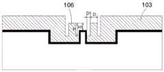
步骤S3.对曝光后的光阻材料层103进行显影处理,以使覆盖在所述上侧结构1021上表面的光阻材料层103全部去除,并使位于所述第二区域110的正下方的光阻材料层103形成上凸形态106。Step S3. Developing the exposed
显影后,覆盖在上侧结构1021的上表面的光阻材料层103全部去除,即脊波导104的上表面的电介质层102完全裸露,同时,由于所述第二区域110的透光率分别小于所述第一区域111和第三区域109的透光率,第二区域110下方的光阻材料层103部分曝光程度较低,而第一区域111和第三区域109下方的光阻材料层103部分的曝光程度较高,所以位于第二区域110的正下方的光阻材料层103形成了上凸形态106,该上凸形态106的上表面的位置处于原有光阻材料层103的上表面与上侧结构1021的上表面之间,且该上凸形态106与侧部结构1022之间间隙设置,上凸形态106与其横向外侧的光阻材料层103之间间隙设置,也就是说,该上凸形态106在凹陷105中是相对独立的。After developing, the
步骤S4.对所述上凸形态106进行热处理,所述上凸形态106自球化,以形成球冠形态107,所述球冠形态107横向上靠近所述脊波导104的边沿位于所述上侧结构1021的上表面的边沿处。Step S4. performing heat treatment on the
如图6所示,对上凸形态106进行热处理,光刻胶发生流动,光阻材料层103与电介质层102两者表面性质不一样,当熔化的光刻胶的液面超过上侧结构1021的上表面时,由于光刻胶的表面张力的作用,上凸形态106受热融化后自球化,从而形成完全覆盖侧部结构1022的球冠形态107;电介质层102的材料可以为氮化硅,回流过程中,液态的光刻胶具有表面张力,通过控制液态光刻胶凸出于上侧结构1021的上表面的高度,可以避免光刻胶溢出。As shown in FIG. 6 , heat treatment is performed on the
需要注意的是,上凸形态106熔化后将向两侧流动,并填充两侧的间隙,通过控制上凸形态106中高于上侧结构1021上表面的部分的体积与两侧间隙的体积之和的比例,可以实现球冠形态107横向上靠近所述脊波导104的边沿位于所述上侧结构1021的上表面的边沿处。例如,在某一比例的实施条件下,熔化后的光刻胶的液面可以处于水平状态,即,融化后的光刻胶的液面刚好上升至与上侧结构的上表面平齐,此时,液态光刻胶的液面趋于水平;在另外的比例的实施条件下,熔化后的光刻胶的液面的顶点高于上侧结构1021的上表面,而液面靠近脊波导104的边沿与上侧结构1021的上表面平齐,即,形成为球冠形态107,且再次增加光刻胶的量,将会有光刻胶溢出到上侧结构1021的上表面,上述二个比例区间范围内的其他比例也可以实现熔化后的光刻胶的液面的顶点高于上侧结构1021的上表面,而液面靠近脊波导104的边沿与上侧结构1021的上表面平齐的目的。It should be noted that, after melting, the
需要注意的是,通过对掩模版进行特定的设计,以及曝光时间等条件的控制,可以使上凸形态106的高度和宽度均为预设的数值,并且,上凸形态106与侧部结构1022之间间隙的宽度,上凸形态106与其横向外侧的光阻材料层103之间间隙的宽度也可以为预设数值。从而在理论上获得预设尺寸的上凸形态106和其两侧的间隙,从而达到球冠形态107不会到达上侧结构1021的上方,只会在底部回流填充上凸形态106与侧部结构1022之间的间隙的目的。上凸形态106转化为球冠形态107,所述球冠形态107横向上靠近所述脊波导104的边沿位于所述上侧结构1021的上表面的边沿处,从而能够对侧部结构1022进行保护,保证电极开窗效果及半导体结构的性能良好。It should be noted that the height and width of the raised
步骤S5.以步骤S4获得的光阻材料层103为掩模对所述电介质层102进行刻蚀,将上侧结构1021去除,以形成电极接触窗口100。Step S5 . Using the
如图7所示,以球冠形态107的光阻材料层103为掩模对电介质层102进行刻蚀,将覆盖在脊波导104的上表面的电介质层102去除,以形成电极接触窗口100。As shown in FIG. 7 , the
在步骤S2中,所述第一区域111由贯穿所述掩模版108的通孔形成;和/或,所述第三区域109由贯穿所述掩模版108的通孔形成。In step S2 , the
所述第一区域111由贯穿所述掩模版108的通孔形成,那么第一区域111的透光率可以为100%,同样的,所述第三区域109也可以由贯穿所述掩模版108的通孔形成,第三区域109的透光率与第一区域111相同,均为100%。曝光时,光可以完全通过第一区域111和第三区域109,而第二区域110的透光率小于100%。The
第一区域111和第三区域109也可以由透光率不为100%的透镜形成。The
在其他的实施方式中,在步骤S2中,所述第二区域110的数量可以为多个,沿横向,所述第一区域111和第三区域109之间的相邻两个第二区域110间隔设置,且间隔的两个第二区域110之间区域的透光率大于所述第二区域110的透光率。In other embodiments, in step S2, the number of the
如图8所示,当第二区域110的数量为一个时,基材101上可以形成一个上凸形态106,而当第一区域111和第三区域109之间的第二区域110为多个,相邻两个第二区域110之间可以具有间隙,即相邻两个第二区域110之间的透光率为100%,基材101上形成的上凸形态106数量也为多个,相邻两个上凸形态106之间具有间隙,多个上凸形态106的表面积增加,从而更容易接受热量,受热后更容易自球化,提高自球化的速度。As shown in Figure 8, when the number of the
所述第一区域111和第三区域109之间任意相邻两个所述第二区域110中,远离所述第一区域111的第二区域110的透光率小于等于靠近所述第一区域111的第二区域110的透光率。In any two adjacent
基材101上脊波导104一侧的上凸形态106为多个,且因为不同的第二区域110的透光程度不同,因此,形成的上凸形态106的高度也不相同,更靠近脊波导104的上凸形态106的高度较低。脊波导104外侧的上凸形态106的数量可以为两个、三个或者更多。当为三个时,由内向外,脊波导104外侧的第一个上凸形态106的高度为3微米,第二个上凸形态106的高度为3.2微米,第三个上凸形态106的高度为3.4微米,其中,上凸形态106的高度为上凸形态106的最高点与凹陷内显影后的光刻胶的最低平面的垂直距离。There are multiple
在一个可以实施的方案中,如图5所示,形成的上凸形态106的数量为一个,且通过控制第一区域111和第三区域109的宽度相同,可以使106左右两侧的间隙的宽度值相同,可以设上凸形态106的顶面与上侧结构1021的上表面之间的高度差为H1、上凸形态106的高度为H、上凸形态106与侧部结构1022之间的横向水平距离为D1,上凸形态106的宽度为D。其中,为了使上凸形态106可以更好的自回流球化,需要使上凸形态106中高于上侧结构1021的上表面的部分的熔化后可以充满两侧的间隙,也就是说,上凸形态106中高于上侧结构1021的上表面的部分的横截面为矩形,该矩形的横截面积为N,以上侧结构1021的上表面为所在位置至间隙的底面之间的距离为高,间隙宽度为宽的矩形的面积为M,上述参数选择符合公式N>2M,即,H1*D>2*D1*(H-H1),其中, H的取值范围可以为2~4微米,D的取值范围可以为0.5~1微米,H1的取值范围可以为0.5~1.5微米, D1的取值范围可以为0.1~0.2微米。光刻技术中,微米级别的实验是完全可以实现的,根据上述公式,经过多次实验,是完全可以获取合理的数据,使图5中的上凸形态106融化后形成图6中的球冠形态。In a possible implementation scheme, as shown in FIG. 5 , the number of convex shapes 106 formed is one, and by controlling the widths of the first region 111 and the third region 109 to be the same, the gaps between the left and right sides of the 106 can be made The width values are the same, the height difference between the top surface of the convex form 106 and the upper surface of the upper side structure 1021 can be set as H1, the height of the convex form 106 is H, and the height difference between the convex form 106 and the side structure 1022 The horizontal horizontal distance is D1, and the width of the convex shape 106 is D. Among them, in order to make the upward convex shape 106 better self-reflux and spherical, it is necessary to make the part of the upward convex shape 106 higher than the upper surface of the upper side structure 1021 be able to fill the gaps on both sides after melting, that is, the upward convex The cross section of the part higher than the upper surface of the upper structure 1021 in the form 106 is rectangular, the cross-sectional area of the rectangle is N, the distance between the upper surface of the upper structure 1021 and the bottom surface of the gap is high, and the gap The area of the rectangle whose width is wide is M, and the above parameter selection conforms to the formula N>2M, that is, H1*D>2*D1*(H-H1), where the value range of H can be 2~4 microns, D The value range of H1 can be 0.5-1 micron, the value range of H1 can be 0.5-1.5 micron, and the value range of D1 can be 0.1-0.2 micron. In photolithography technology, micron-level experiments are completely achievable. According to the above formula, after many experiments, it is completely possible to obtain reasonable data, so that the
在步骤S4中,对所述上凸形态106进行热处理包括以下步骤:In step S4, performing heat treatment on the
步骤S41.前序烘胶处理,在第一温度范围下烘烤上凸形态106,其中,第一温度范围可以为92-98℃,烘干的时间可以为30-40秒。去除上凸形态106中多余溶剂,提高光刻胶黏附力,并冷却至室温。Step S41 . Pre-baking glue treatment, baking the
步骤S42.回流烘烤,以第一加热速率将烘烤温度提升至第一温度,维持第一时间后冷却至室温;然后以第二加热速率将烘烤温度提升至第二温度,维持第二时间后冷却至室温,且第一加热速率大于第二加热速率。具体的,回流烘烤温度,第一阶段加热到145℃,加热速率4℃/s,维持大致3min后冷却至室温;第二阶段,加热到153℃,加热速率10℃/min,维持大致2min左右冷却至室温,迁移后的光刻胶的胶形变得平滑,对凹陷105和预留结构的区域实现充分的保护。因为在光刻胶的熔化过程中,需要将上凸形态106的绝大部分熔化,因此,实验过程中的加热温度相对较高,且加热时间相对较长,回流烘烤过程中,加热速率是变化的,前期加热速率大,升温较快,光刻胶可以快速达到较高温度,快速熔化后有利于快速回流填充,回流达到一定程度后冷却定型;而第二阶段再次烘烤,这个阶段时,加热速率小,缓慢达到最高温度,并且在最高温度处维持的时间较短,防止过快加热,光刻胶回流过快超过脊波导104的顶部。Step S42. Reflow baking, raising the baking temperature to the first temperature at the first heating rate, cooling to room temperature after maintaining the first time; then raising the baking temperature to the second temperature at the second heating rate, maintaining the second temperature Cool to room temperature after a period of time, and the first heating rate is greater than the second heating rate. Specifically, the reflow baking temperature is heated to 145°C in the first stage, with a heating rate of 4°C/s, maintained for approximately 3 minutes and then cooled to room temperature; in the second stage, heated to 153°C, with a heating rate of 10°C/min, maintained for approximately 2 minutes After cooling down to room temperature, the shape of the migrated photoresist becomes smooth, which fully protects the
如图9和图10所示,本发明实施例提供的半导体器件的制备方法,包括上述的电极接触窗口的制作方法中的步骤S1~S5,在步骤S5之后,还包括去除所述电介质层102的表面的光阻材料层103,并在电极接触窗口100的表面形成导电金属层112的步骤。As shown in FIG. 9 and FIG. 10 , the method for manufacturing a semiconductor device provided by the embodiment of the present invention includes steps S1 to S5 in the above-mentioned method for making an electrode contact window, and after step S5, further includes removing the dielectric layer 102 A step of forming a
最后应说明的是:以上各实施例仅用以说明本发明的技术方案,而非对其限制;尽管参照前述各实施例对本发明进行了详细的说明,本领域的普通技术人员应当理解:其依然可以对前述各实施例所记载的技术方案进行修改,或者对其中部分或者全部技术特征进行等同替换;而这些修改或者替换,并不使相应技术方案的本质脱离本发明各实施例技术方案的范围。Finally, it should be noted that: the above embodiments are only used to illustrate the technical solutions of the present invention, rather than limiting them; although the present invention has been described in detail with reference to the foregoing embodiments, those of ordinary skill in the art should understand that: It is still possible to modify the technical solutions described in the foregoing embodiments, or perform equivalent replacements for some or all of the technical features; and these modifications or replacements do not make the essence of the corresponding technical solutions deviate from the technical solutions of the various embodiments of the present invention. scope.
Claims (9)
Translated fromChinesePriority Applications (1)
| Application Number | Priority Date | Filing Date | Title |
|---|---|---|---|
| CN202210249550.1ACN114336275B (en) | 2022-03-15 | 2022-03-15 | Manufacturing method of electrode contact window and preparation method of semiconductor device |
Applications Claiming Priority (1)
| Application Number | Priority Date | Filing Date | Title |
|---|---|---|---|
| CN202210249550.1ACN114336275B (en) | 2022-03-15 | 2022-03-15 | Manufacturing method of electrode contact window and preparation method of semiconductor device |
Publications (2)
| Publication Number | Publication Date |
|---|---|
| CN114336275A CN114336275A (en) | 2022-04-12 |
| CN114336275Btrue CN114336275B (en) | 2023-02-21 |
Family
ID=81033538
Family Applications (1)
| Application Number | Title | Priority Date | Filing Date |
|---|---|---|---|
| CN202210249550.1AActiveCN114336275B (en) | 2022-03-15 | 2022-03-15 | Manufacturing method of electrode contact window and preparation method of semiconductor device |
Country Status (1)
| Country | Link |
|---|---|
| CN (1) | CN114336275B (en) |
Families Citing this family (1)
| Publication number | Priority date | Publication date | Assignee | Title |
|---|---|---|---|---|
| CN118801207B (en)* | 2024-09-13 | 2025-02-07 | 度亘核芯光电技术(苏州)有限公司 | Semiconductor laser manufacturing method and semiconductor laser |
Citations (6)
| Publication number | Priority date | Publication date | Assignee | Title |
|---|---|---|---|---|
| CN1188327A (en)* | 1996-11-13 | 1998-07-22 | 世界先进积体电路股份有限公司 | Method of Forming Contact Window |
| CN1262539A (en)* | 1999-01-25 | 2000-08-09 | 财团法人工业技术研究院 | Manufacturing method of ridge optical waveguide semiconductor light emitting element |
| TWI245379B (en)* | 2004-05-19 | 2005-12-11 | Sanyo Electric Co | Semiconductor device and method for manufacturing same |
| CN107257082A (en)* | 2017-07-05 | 2017-10-17 | 青岛海信宽带多媒体技术有限公司 | A kind of preparation method of ridge waveguide laser electrode contact window |
| CN108847574A (en)* | 2018-06-26 | 2018-11-20 | 华慧芯科技(天津)有限公司 | A kind of method of ridge ripple conductive electrode windowing |
| CN112038218A (en)* | 2020-09-04 | 2020-12-04 | 武汉敏芯半导体股份有限公司 | Preparation process of ridge waveguide DFB laser based on double-glue-layer structure |
- 2022
- 2022-03-15CNCN202210249550.1Apatent/CN114336275B/enactiveActive
Patent Citations (6)
| Publication number | Priority date | Publication date | Assignee | Title |
|---|---|---|---|---|
| CN1188327A (en)* | 1996-11-13 | 1998-07-22 | 世界先进积体电路股份有限公司 | Method of Forming Contact Window |
| CN1262539A (en)* | 1999-01-25 | 2000-08-09 | 财团法人工业技术研究院 | Manufacturing method of ridge optical waveguide semiconductor light emitting element |
| TWI245379B (en)* | 2004-05-19 | 2005-12-11 | Sanyo Electric Co | Semiconductor device and method for manufacturing same |
| CN107257082A (en)* | 2017-07-05 | 2017-10-17 | 青岛海信宽带多媒体技术有限公司 | A kind of preparation method of ridge waveguide laser electrode contact window |
| CN108847574A (en)* | 2018-06-26 | 2018-11-20 | 华慧芯科技(天津)有限公司 | A kind of method of ridge ripple conductive electrode windowing |
| CN112038218A (en)* | 2020-09-04 | 2020-12-04 | 武汉敏芯半导体股份有限公司 | Preparation process of ridge waveguide DFB laser based on double-glue-layer structure |
Also Published As
| Publication number | Publication date |
|---|---|
| CN114336275A (en) | 2022-04-12 |
Similar Documents
| Publication | Publication Date | Title |
|---|---|---|
| US6172791B1 (en) | Electro-optic modulators | |
| US9759939B2 (en) | Liquid crystal display device and fabrication method of a conductive substrate | |
| CN107257082B (en) | Manufacturing method of electrode contact window of ridge waveguide laser | |
| US9595548B2 (en) | Method of manufacturing thin film transistor substrate having etched trenches with color filter material disposed therein | |
| CN114336276B (en) | Manufacturing method of electrode contact window and manufacturing method of semiconductor structure | |
| CN114336275B (en) | Manufacturing method of electrode contact window and preparation method of semiconductor device | |
| CN109256397B (en) | Display substrate, preparation method thereof and display device | |
| CN108538856B (en) | Array substrate and manufacturing method thereof | |
| CN111446260B (en) | Array substrate, manufacturing method thereof, and display device | |
| CN110767539A (en) | A display substrate, its manufacturing method, and a display device | |
| CN114628877B (en) | Method for preparing semiconductor structure | |
| CN115185038B (en) | Semiconductor device and manufacturing method thereof | |
| CN110429061B (en) | Display substrate, manufacturing method thereof and display device | |
| CN116092942A (en) | Manufacturing method of power semiconductor device and power semiconductor device | |
| CN112164980A (en) | Ridge passivation method of DFB chip | |
| CN112542472B (en) | Display panel and manufacturing method thereof | |
| CN101159276A (en) | Pixel structure and manufacturing method thereof | |
| KR940010596B1 (en) | Method of wet etching for thermal oxide | |
| TWI862179B (en) | Display device and manufacturing method of display device | |
| CN118825172A (en) | Intermediate state micro display device, micro display device and preparation method thereof | |
| CN117276328A (en) | Trench gate field effect transistor | |
| CN119322392A (en) | Semiconductor structure and forming method thereof | |
| KR20250139196A (en) | Embedded lens structures and the methods of forming the same | |
| CN116130353A (en) | Method for forming trench structure with complex geometric section on semiconductor surface | |
| CN114815426A (en) | Array substrate and display panel |
Legal Events
| Date | Code | Title | Description |
|---|---|---|---|
| PB01 | Publication | ||
| PB01 | Publication | ||
| SE01 | Entry into force of request for substantive examination | ||
| SE01 | Entry into force of request for substantive examination | ||
| GR01 | Patent grant | ||
| GR01 | Patent grant | ||
| CP03 | Change of name, title or address | ||
| CP03 | Change of name, title or address | Address after:Building 32, Northeast Zone, No. 99 Jinjihu Avenue, Industrial Park, Suzhou City, Jiangsu Province, 215000 Patentee after:DuGen Core Optoelectronic Technology (Suzhou) Co.,Ltd. Country or region after:China Address before:215000 rooms 215 and 217, building 20, Northwest District, 99 Jinjihu Avenue, Suzhou Industrial Park, Jiangsu Province Patentee before:DUGEN LASER TECHNOLOGY (SUZHOU) Co.,Ltd. Country or region before:China |