CN114335331A - Semiconductor element and manufacturing method thereof - Google Patents
Semiconductor element and manufacturing method thereofDownload PDFInfo
- Publication number
- CN114335331A CN114335331ACN202011083857.6ACN202011083857ACN114335331ACN 114335331 ACN114335331 ACN 114335331ACN 202011083857 ACN202011083857 ACN 202011083857ACN 114335331 ACN114335331 ACN 114335331A
- Authority
- CN
- China
- Prior art keywords
- layer
- spacer
- metal
- upper electrode
- forming
- Prior art date
- Legal status (The legal status is an assumption and is not a legal conclusion. Google has not performed a legal analysis and makes no representation as to the accuracy of the status listed.)
- Pending
Links
- 238000004519manufacturing processMethods0.000titleclaimsabstractdescription24
- 239000004065semiconductorSubstances0.000titleclaimsabstractdescription23
- 229910052751metalInorganic materials0.000claimsabstractdescription92
- 239000002184metalSubstances0.000claimsabstractdescription92
- 230000001681protective effectEffects0.000claimsabstractdescription48
- 238000000034methodMethods0.000claimsabstractdescription44
- 230000005291magnetic effectEffects0.000claimsabstractdescription30
- 239000000758substrateSubstances0.000claimsabstractdescription16
- 230000005641tunnelingEffects0.000claimsabstractdescription14
- 238000000059patterningMethods0.000claimsabstractdescription3
- 125000006850spacer groupChemical group0.000claimsdescription60
- 239000010410layerSubstances0.000description139
- 230000008569processEffects0.000description27
- 238000005530etchingMethods0.000description11
- 230000004888barrier functionEffects0.000description10
- 239000010949copperSubstances0.000description9
- IJGRMHOSHXDMSA-UHFFFAOYSA-NAtomic nitrogenChemical compoundN#NIJGRMHOSHXDMSA-UHFFFAOYSA-N0.000description8
- XUIMIQQOPSSXEZ-UHFFFAOYSA-NSiliconChemical compound[Si]XUIMIQQOPSSXEZ-UHFFFAOYSA-N0.000description8
- 229910052710siliconInorganic materials0.000description8
- 239000010703siliconSubstances0.000description8
- 229910052715tantalumInorganic materials0.000description8
- GUVRBAGPIYLISA-UHFFFAOYSA-Ntantalum atomChemical compound[Ta]GUVRBAGPIYLISA-UHFFFAOYSA-N0.000description8
- 239000004020conductorSubstances0.000description7
- 239000000463materialSubstances0.000description7
- 229910052581Si3N4Inorganic materials0.000description6
- 239000011229interlayerSubstances0.000description6
- HQVNEWCFYHHQES-UHFFFAOYSA-Nsilicon nitrideChemical compoundN12[Si]34N5[Si]62N3[Si]51N64HQVNEWCFYHHQES-UHFFFAOYSA-N0.000description6
- 239000010936titaniumSubstances0.000description6
- RYGMFSIKBFXOCR-UHFFFAOYSA-NCopperChemical compound[Cu]RYGMFSIKBFXOCR-UHFFFAOYSA-N0.000description5
- NRTOMJZYCJJWKI-UHFFFAOYSA-NTitanium nitrideChemical compound[Ti]#NNRTOMJZYCJJWKI-UHFFFAOYSA-N0.000description5
- 229910052802copperInorganic materials0.000description5
- 229910052782aluminiumInorganic materials0.000description4
- XAGFODPZIPBFFR-UHFFFAOYSA-NaluminiumChemical compound[Al]XAGFODPZIPBFFR-UHFFFAOYSA-N0.000description4
- -1but not limited toSubstances0.000description4
- 238000010586diagramMethods0.000description4
- 239000003989dielectric materialSubstances0.000description4
- 230000009977dual effectEffects0.000description4
- 230000000694effectsEffects0.000description4
- 238000005516engineering processMethods0.000description4
- 229910052757nitrogenInorganic materials0.000description4
- WFKWXMTUELFFGS-UHFFFAOYSA-NtungstenChemical compound[W]WFKWXMTUELFFGS-UHFFFAOYSA-N0.000description4
- 229910052721tungstenInorganic materials0.000description4
- 239000010937tungstenSubstances0.000description4
- 229910000838Al alloyInorganic materials0.000description3
- XEEYBQQBJWHFJM-UHFFFAOYSA-NIronChemical compound[Fe]XEEYBQQBJWHFJM-UHFFFAOYSA-N0.000description3
- RTAQQCXQSZGOHL-UHFFFAOYSA-NTitaniumChemical compound[Ti]RTAQQCXQSZGOHL-UHFFFAOYSA-N0.000description3
- HMDDXIMCDZRSNE-UHFFFAOYSA-N[C].[Si]Chemical compound[C].[Si]HMDDXIMCDZRSNE-UHFFFAOYSA-N0.000description3
- UQZIWOQVLUASCR-UHFFFAOYSA-Nalumane;titaniumChemical compound[AlH3].[Ti]UQZIWOQVLUASCR-UHFFFAOYSA-N0.000description3
- JPNWDVUTVSTKMV-UHFFFAOYSA-Ncobalt tungstenChemical compound[Co].[W]JPNWDVUTVSTKMV-UHFFFAOYSA-N0.000description3
- 238000010884ion-beam techniqueMethods0.000description3
- 230000004048modificationEffects0.000description3
- 238000012986modificationMethods0.000description3
- 150000004767nitridesChemical class0.000description3
- 229920002120photoresistant polymerPolymers0.000description3
- 238000001020plasma etchingMethods0.000description3
- BASFCYQUMIYNBI-UHFFFAOYSA-NplatinumChemical compound[Pt]BASFCYQUMIYNBI-UHFFFAOYSA-N0.000description3
- MZLGASXMSKOWSE-UHFFFAOYSA-Ntantalum nitrideChemical compound[Ta]#NMZLGASXMSKOWSE-UHFFFAOYSA-N0.000description3
- 229910052719titaniumInorganic materials0.000description3
- JBRZTFJDHDCESZ-UHFFFAOYSA-NAsGaChemical compound[As]#[Ga]JBRZTFJDHDCESZ-UHFFFAOYSA-N0.000description2
- 229910019236CoFeBInorganic materials0.000description2
- 229910001218Gallium arsenideInorganic materials0.000description2
- PXHVJJICTQNCMI-UHFFFAOYSA-NNickelChemical compound[Ni]PXHVJJICTQNCMI-UHFFFAOYSA-N0.000description2
- VYPSYNLAJGMNEJ-UHFFFAOYSA-NSilicium dioxideChemical compoundO=[Si]=OVYPSYNLAJGMNEJ-UHFFFAOYSA-N0.000description2
- BOTDANWDWHJENH-UHFFFAOYSA-NTetraethyl orthosilicateChemical compoundCCO[Si](OCC)(OCC)OCCBOTDANWDWHJENH-UHFFFAOYSA-N0.000description2
- ZDZZPLGHBXACDA-UHFFFAOYSA-N[B].[Fe].[Co]Chemical compound[B].[Fe].[Co]ZDZZPLGHBXACDA-UHFFFAOYSA-N0.000description2
- 230000005290antiferromagnetic effectEffects0.000description2
- 229910017052cobaltInorganic materials0.000description2
- 239000010941cobaltSubstances0.000description2
- GUTLYIVDDKVIGB-UHFFFAOYSA-Ncobalt atomChemical compound[Co]GUTLYIVDDKVIGB-UHFFFAOYSA-N0.000description2
- 239000003302ferromagnetic materialSubstances0.000description2
- 239000010931goldSubstances0.000description2
- SHMWNGFNWYELHA-UHFFFAOYSA-Niridium manganeseChemical compound[Mn].[Ir]SHMWNGFNWYELHA-UHFFFAOYSA-N0.000description2
- CPLXHLVBOLITMK-UHFFFAOYSA-Nmagnesium oxideInorganic materials[Mg]=OCPLXHLVBOLITMK-UHFFFAOYSA-N0.000description2
- 239000000395magnesium oxideSubstances0.000description2
- AXZKOIWUVFPNLO-UHFFFAOYSA-Nmagnesium;oxygen(2-)Chemical compound[O-2].[Mg+2]AXZKOIWUVFPNLO-UHFFFAOYSA-N0.000description2
- 230000005415magnetizationEffects0.000description2
- 229910000480nickel oxideInorganic materials0.000description2
- 238000000206photolithographyMethods0.000description2
- 230000000717retained effectEffects0.000description2
- 229910052814silicon oxideInorganic materials0.000description2
- 239000000126substanceSubstances0.000description2
- 229910015136FeMnInorganic materials0.000description1
- 229910000577Silicon-germaniumInorganic materials0.000description1
- LEVVHYCKPQWKOP-UHFFFAOYSA-N[Si].[Ge]Chemical compound[Si].[Ge]LEVVHYCKPQWKOP-UHFFFAOYSA-N0.000description1
- 229910045601alloyInorganic materials0.000description1
- 239000000956alloySubstances0.000description1
- 230000008901benefitEffects0.000description1
- 230000008859changeEffects0.000description1
- 238000004140cleaningMethods0.000description1
- FQMNUIZEFUVPNU-UHFFFAOYSA-Ncobalt ironChemical compound[Fe].[Co].[Co]FQMNUIZEFUVPNU-UHFFFAOYSA-N0.000description1
- 239000002131composite materialSubstances0.000description1
- 230000005611electricityEffects0.000description1
- 230000003628erosive effectEffects0.000description1
- 229910052732germaniumInorganic materials0.000description1
- GNPVGFCGXDBREM-UHFFFAOYSA-Ngermanium atomChemical compound[Ge]GNPVGFCGXDBREM-UHFFFAOYSA-N0.000description1
- PCHJSUWPFVWCPO-UHFFFAOYSA-NgoldChemical compound[Au]PCHJSUWPFVWCPO-UHFFFAOYSA-N0.000description1
- 229910052737goldInorganic materials0.000description1
- 230000006872improvementEffects0.000description1
- 239000011810insulating materialSubstances0.000description1
- 229910052742ironInorganic materials0.000description1
- DALUDRGQOYMVLD-UHFFFAOYSA-Niron manganeseChemical compound[Mn].[Fe]DALUDRGQOYMVLD-UHFFFAOYSA-N0.000description1
- IGOJMROYPFZEOR-UHFFFAOYSA-Nmanganese platinumChemical compound[Mn].[Pt]IGOJMROYPFZEOR-UHFFFAOYSA-N0.000description1
- 229910044991metal oxideInorganic materials0.000description1
- 150000004706metal oxidesChemical class0.000description1
- 229910052759nickelInorganic materials0.000description1
- TWNQGVIAIRXVLR-UHFFFAOYSA-Noxo(oxoalumanyloxy)alumaneChemical compoundO=[Al]O[Al]=OTWNQGVIAIRXVLR-UHFFFAOYSA-N0.000description1
- GNRSAWUEBMWBQH-UHFFFAOYSA-NoxonickelChemical compound[Ni]=OGNRSAWUEBMWBQH-UHFFFAOYSA-N0.000description1
- 229910052697platinumInorganic materials0.000description1
- 238000005498polishingMethods0.000description1
- 238000007517polishing processMethods0.000description1
- 230000035945sensitivityEffects0.000description1
- HBMJWWWQQXIZIP-UHFFFAOYSA-Nsilicon carbideChemical compound[Si+]#[C-]HBMJWWWQQXIZIP-UHFFFAOYSA-N0.000description1
- 229910010271silicon carbideInorganic materials0.000description1
Images


Classifications
- H—ELECTRICITY
- H10—SEMICONDUCTOR DEVICES; ELECTRIC SOLID-STATE DEVICES NOT OTHERWISE PROVIDED FOR
- H10N—ELECTRIC SOLID-STATE DEVICES NOT OTHERWISE PROVIDED FOR
- H10N50/00—Galvanomagnetic devices
- H10N50/80—Constructional details
- H—ELECTRICITY
- H10—SEMICONDUCTOR DEVICES; ELECTRIC SOLID-STATE DEVICES NOT OTHERWISE PROVIDED FOR
- H10N—ELECTRIC SOLID-STATE DEVICES NOT OTHERWISE PROVIDED FOR
- H10N50/00—Galvanomagnetic devices
- H10N50/01—Manufacture or treatment
- H—ELECTRICITY
- H10—SEMICONDUCTOR DEVICES; ELECTRIC SOLID-STATE DEVICES NOT OTHERWISE PROVIDED FOR
- H10N—ELECTRIC SOLID-STATE DEVICES NOT OTHERWISE PROVIDED FOR
- H10N50/00—Galvanomagnetic devices
- H10N50/10—Magnetoresistive devices
- H—ELECTRICITY
- H10—SEMICONDUCTOR DEVICES; ELECTRIC SOLID-STATE DEVICES NOT OTHERWISE PROVIDED FOR
- H10B—ELECTRONIC MEMORY DEVICES
- H10B61/00—Magnetic memory devices, e.g. magnetoresistive RAM [MRAM] devices
Landscapes
- Engineering & Computer Science (AREA)
- Manufacturing & Machinery (AREA)
- Internal Circuitry In Semiconductor Integrated Circuit Devices (AREA)
- Mram Or Spin Memory Techniques (AREA)
- Hall/Mr Elements (AREA)
Abstract
Description
Translated fromChinese技术领域technical field
本发明涉及一种制作半导体元件,尤其是涉及一种制作磁阻式随机存取存储器(magnetoresistive random access memory,MRAM)元件的方法。The present invention relates to a method for manufacturing a semiconductor element, in particular to a method for manufacturing a magnetoresistive random access memory (MRAM) element.
背景技术Background technique
已知,磁阻(magnetoresistance,MR)效应是材料的电阻随着外加磁场的变化而改变的效应,其物理量的定义,是在有无磁场下的电阻差除上原先电阻,用以代表电阻变化率。目前,磁阻效应已被成功地运用在硬盘生产上,具有重要的商业应用价值。此外,利用巨磁电阻物质在不同的磁化状态下具有不同电阻值的特点,还可以制成磁性随机存储器(MRAM),其优点是在不通电的情况下可以继续保留存储的数据。It is known that the magnetoresistance (MR) effect is the effect that the resistance of the material changes with the change of the external magnetic field. Rate. At present, the magnetoresistance effect has been successfully used in the production of hard disks and has important commercial application value. In addition, magnetic random access memory (MRAM) can also be made by using the characteristics of giant magnetoresistive materials with different resistance values in different magnetization states, which has the advantage that the stored data can continue to be retained without electricity.
上述磁阻效应还被应用在磁场感测(magnetic field sensor)领域,例如,移动电话中搭配全球定位系统(global positioning system,GPS)的电子罗盘(electroniccompass)零组件,用来提供使用者移动方位等信息。目前,市场上已有各式的磁场感测技术,例如,各向异性磁阻(anisotropic magnetoresistance,AMR)感测元件、巨磁阻(GMR)感测元件、磁隧穿结(magnetic tunneling junction,MTJ)感测元件等等。然而,上述现有技术的缺点通常包括:较占芯片面积、制作工艺较昂贵、较耗电、灵敏度不足,以及易受温度变化影响等等,而有必要进一步改进。The above magnetoresistive effect is also applied in the field of magnetic field sensor, for example, the electronic compass (electronic compass) component in a mobile phone with a global positioning system (GPS) is used to provide the user's moving position and other information. At present, there are various magnetic field sensing technologies on the market, such as anisotropic magnetoresistance (AMR) sensing elements, giant magnetoresistance (GMR) sensing elements, magnetic tunneling junction (magnetic tunneling junction) MTJ) sensing element and so on. However, the disadvantages of the above-mentioned prior art usually include: occupying a larger chip area, more expensive manufacturing process, higher power consumption, insufficient sensitivity, and being easily affected by temperature changes, etc., and further improvement is necessary.
发明内容SUMMARY OF THE INVENTION
本发明一实施例揭露一种制作半导体元件的方法。首先形成一第一金属间介电层于基底上以及一第一金属内连线于第一金属间介电层内,然后形成磁性隧穿结(magnetictunneling junction,MTJ)以及一上电极于第一金属内连线上,形成间隙壁于MTJ以及上电极旁,形成一第二金属间介电层环绕间隙壁,形成一遮盖层于上电极、间隙壁及第二金属间介电层上,再图案化遮盖层以形成保护盖于上电极及间隙壁上。An embodiment of the present invention discloses a method of fabricating a semiconductor device. First, a first IMD layer is formed on the substrate and a first metal interconnect is formed in the first IMD layer, and then a magnetic tunneling junction (MTJ) and an upper electrode are formed on the first IMD layer. On the metal interconnection line, a spacer is formed beside the MTJ and the upper electrode, a second inter-metal dielectric layer is formed to surround the spacer, a cover layer is formed on the upper electrode, the spacer and the second inter-metal dielectric layer, and then The cover layer is patterned to form a protective cover on the upper electrode and the spacer.
本发明另一实施例揭露一种半导体元件,其主要包含一磁性隧穿结(magnetictunneling junction,MTJ)设于基底上、上电极设于MTJ上以及一保护盖设于上电极上。Another embodiment of the present invention discloses a semiconductor device, which mainly includes a magnetic tunneling junction (MTJ) disposed on a substrate, an upper electrode disposed on the MTJ, and a protective cover disposed on the upper electrode.
本发明又一实施例揭露一种半导体元件,其主要包含一磁性隧穿结(magnetictunneling junction,MTJ)设于基底上、上电极设于MTJ上、间隙壁设于MTJ以及上电极旁以及一保护盖设于上电极及间隙壁上。Yet another embodiment of the present invention discloses a semiconductor device, which mainly includes a magnetic tunneling junction (MTJ) disposed on a substrate, an upper electrode disposed on the MTJ, a spacer disposed next to the MTJ and the upper electrode, and a protection The cover is arranged on the upper electrode and the spacer.
附图说明Description of drawings
图1至图6为本发明一实施例制作一MRAM单元的方式示意图;1 to 6 are schematic diagrams of a method for fabricating an MRAM cell according to an embodiment of the present invention;
图7至图10为本发明一实施例制作一MRAM单元的方式示意图。7 to 10 are schematic diagrams of a method for fabricating an MRAM cell according to an embodiment of the present invention.
主要元件符号说明Description of main component symbols
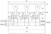
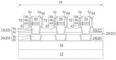
12:基底12: Base
14:MRAM区域14: MRAM area
18:层间介电层18: Interlayer dielectric layer
20:金属内连线结构20: Metal interconnect structure
22:金属内连线结构22: Metal interconnect structure
24:金属间介电层24: Intermetal dielectric layer
26:金属内连线26: Metal interconnect
28:停止层28: Stop Layer
30:金属间介电层30: Intermetal dielectric layer
32:金属内连线32: Metal interconnect
34:阻障层34: Barrier layer
36:金属层36: Metal layer
38:MTJ堆叠结构38: MTJ stack structure
42:下电极42: Lower electrode
44:固定层44: Fixed layer
46:阻障层46: Barrier layer
48:自由层48: Free Layer
50:上电极50: Upper electrode
52:MTJ52: MTJ
54:间隙壁54: Spacer
56:金属介电层56: Metal dielectric layer
58:遮盖层58: Covering Layer
60:图案化掩模60: Patterned Mask
62:开口62: Opening
64:保护盖64: Protective cover
66:金属间介电层66: Intermetal dielectric layer
68:停止层68: Stop Layer
70:金属间介电层70: Intermetal dielectric layer
72:金属内连线72: Metal interconnect
74:停止层74: Stop Layer
具体实施方式Detailed ways
请参照图1至图6,图1至图6为本发明一实施例制作一MRAM单元的方式示意图。如图1所示,首先提供一基底12,例如一由半导体材料所构成的基底12,其中半导体材料可选自由硅、锗、硅锗复合物、硅碳化物(silicon carbide)、砷化镓(gallium arsenide)等所构成的群组,且基底12上较佳定义有一MRAM区域14以及一逻辑区域(图未示)。Please refer to FIGS. 1 to 6 . FIGS. 1 to 6 are schematic diagrams of a method for fabricating an MRAM cell according to an embodiment of the present invention. As shown in FIG. 1 , a
基底12上可包含例如金属氧化物半导体(metal-oxide semiconductor,MOS)晶体管等主动(有源)元件、被动(无源)元件、导电层以及例如层间介电层(interlayerdielectric,ILD)18等介电层覆盖于其上。更具体而言,基底12上可包含平面型或非平面型(如鳍状结构晶体管)等MOS晶体管元件,其中MOS晶体管可包含栅极结构(例如金属栅极)以及源极/漏极区域、间隙壁、外延层、接触洞蚀刻停止层等晶体管元件,层间介电层18可设于基底12上并覆盖MOS晶体管,且层间介电层18可具有多个接触插塞电连接MOS晶体管的栅极以及/或源极/漏极区域。由于平面型或非平面型晶体管与层间介电层等相关制作工艺均为本领域所熟知技术,在此不另加赘述。The
然后于层间介电层18上依序形成金属内连线结构20、22电连接前述的接触插塞,其中金属内连线结构20包含一金属间介电层24以及金属内连线26镶嵌于金属间介电层24中,金属内连线结构22则包含一停止层28、一金属间介电层30以及金属内连线32镶嵌于停止层28与金属间介电层30中。Then,
在本实施例中,金属内连线结构20中的各金属内连线26较佳包含一沟槽导体(trench conductor),金属内连线结构22中设于MRAM区域14的金属内连线32则包含接触洞导体(via conductor)。另外各金属内连线结构20、22中的各金属内连线26、32均可依据单镶嵌制作工艺或双镶嵌制作工艺镶嵌于金属间介电层24、30以及/或停止层28中并彼此电连接。例如各金属内连线26、32可更细部包含一阻障层34以及一金属层36,其中阻障层34可选自由钛(Ti)、氮化钛(TiN)、钽(Ta)以及氮化钽(TaN)所构成的群组,而金属层36可选自由钨(W)、铜(Cu)、铝(Al)、钛铝合金(TiAl)、钴钨磷化物(cobalt tungsten phosphide,CoWP)等所构成的群组,但不局限于此。由于单镶嵌或双镶嵌制作工艺是本领域所熟知技术,在此不另加赘述。此外在本实例金属内连线26中的金属层36较佳包含铜、金属内连线32中的金属层36较佳包含钨、金属间介电层24、30较佳包含氧化硅例如四乙氧基硅烷(tetraethylorthosilicate,TEOS)、而停止层28则包含氮掺杂碳化物层(nitrogen doped carbide,NDC)、氮化硅、或氮碳化硅(silicon carbon nitride,SiCN),但不局限于此。In the present embodiment, each metal interconnect 26 in the
接着形成一下电极42、一MTJ堆叠结构38、一上电极50以及一图案化掩模(图未示)于金属内连线结构22上。在本实施例中,形成MTJ堆叠结构38的方式可先依序形成一固定层(pinned layer)44、一阻障层(barrier layer)46以及一自由层(free layer)48于下电极42上。在本实施例中,下电极42及上电极50较佳包含导电材料,例如但不局限于钽(Ta)、氮化钽(TaN)、铂(Pt)、铜(Cu)、金(Au)、铝(Al)。固定层44可包含铁磁性材料例如但不局限于钴铁硼(cobalt-iron-boron,CoFeB)、钴铁(cobalt-iron,CoFe)、铁(Fe)、钴(Co)等。此外,固定层44也可以是由反铁磁性(antiferromagnetic,AFM)材料所构成者,例如铁锰(FeMn)、铂锰(PtMn)、铱锰(IrMn)、氧化镍(NiO)等,用以固定或限制邻近层的磁矩方向。阻障层46可由包含氧化物的绝缘材料所构成,例如氧化铝(AlOx)或氧化镁(MgO),但均不局限于此。自由层48可以是由铁磁性材料所构成者,例如铁、钴、镍或其合金如钴铁硼(cobalt-iron-boron,CoFeB),但不限于此。其中,自由层48的磁化方向会受外部磁场而「自由」改变。Next, a
随后如图2所示,利用图案化掩模,例如图案化光致抗蚀剂为掩模进行一道或一道以上蚀刻制作工艺去除部分上电极50、部分MTJ堆叠结构38、部分下电极42以及部分金属间介电层30以形成多个MTJ 52于金属内连线32上,其中本实施例虽于MRAM区域14形成三组MTJ 52为例,但MTJ 52的数量均可视制作工艺需求调整并不局限于此。需注意的是,本实施例于图案化上述上电极50、MTJ堆叠结构38、下电极42及金属间介电层30所进行的蚀刻制作工艺可包含反应性离子蚀刻制作工艺(reactive ion etching,RIE)以及/或离子束蚀刻制作工艺(ion beam etching,IBE),由于离子束蚀刻制作工艺的特性,剩余的金属间介电层30上表面较佳略低于金属内连线32上表面且金属间介电层30上表面较佳呈现一弧形或曲面。另外又需注意的是,本实施例利用离子束蚀刻制作工艺去除部分金属间介电层30的时候较佳一同去除部分金属内连线32,使金属内连线32靠近MTJ 62的交界处形成倾斜侧壁。Then, as shown in FIG. 2 , using a patterned mask, such as a patterned photoresist as a mask, one or more etching processes are performed to remove part of the
然后形成一遮盖层(图未示)于MTJ 52上并覆盖金属间介电层30表面,再利用回蚀刻去除部分遮盖层以形成间隙壁54于各MTJ 52侧壁。在本实施例中,间隙壁54较佳包含氮化硅,但又可依据制作工艺需求选用其他介电材料例如但不局限于氧化硅、氮氧化硅或氮碳化硅。Then, a capping layer (not shown) is formed on the
接着如图3所示,先形成一金属间介电层56于各MTJ 52上环绕间隙壁54,再形成一遮盖层58于上电极50、间隙壁54以及金属间介电层56上,其中遮盖层58较佳依据下方的元件具有上下起伏,例如设于金属间介电层56上方的遮盖层58顶部便略低于设于上电极50上方的遮盖层58顶部。在本实施例中,金属间介电层56较佳包含一超低介电常数介电层,例如可包含多孔性介电材料例如但不局限于氧碳化硅(SiOC)或氧碳化硅氢(SiOCH),而遮盖层58则较佳包含导电材料或更具体而言金属或金属氮化物例如但不局限于钽或氮化钛。Next, as shown in FIG. 3 , an
如图4所示,然后形成一图案化掩模60例如图案化光致抗蚀剂于遮盖层58上,其中图案化光致抗蚀剂包含多个开口62暴露出部分遮盖层58表面。接着利用图案化掩模60为掩模去除部分遮盖层58以形成保护盖64于各MTJ 52或上电极50正上方。在本实施例中,各保护盖64侧壁虽较佳切齐下方的间隙壁54的外侧侧壁,但不局限于此,依据本发明其他实施例各保护盖64侧壁又可选择不切齐下方的间隙壁54外侧侧壁例如保护盖64可同时覆盖于间隙壁54及金属间介电层56上,此变化型也属本发明所涵盖的范围。As shown in FIG. 4 , a patterned
随后如图5所示,先去除图案化掩模60,进行一湿式清洗制作工艺去除保护盖64表面以及周围的部分残余物,再形成另一金属间介电层66完全覆盖保护盖64并搭配进行一平坦化制作工艺例如以化学机械研磨制作工艺去除部分金属间介电层66使剩余的金属间介电层66具有平坦表面同时金属间介电层66顶部仍高于保护盖64顶部。如同金属间介电层56,金属间介电层66可包含一超低介电常数介电层,例如可包含多孔性介电材料例如但不局限于氧碳化硅(SiOC)或氧碳化硅氢(SiOCH)。Then, as shown in FIG. 5 , the patterned
然后如图6所示,先形成一停止层68于金属间介电层66上,形成一金属间介电层70于停止层68上,进行一道或一道以上光刻暨蚀刻制作工艺去除部分金属间介电层70、部分停止层68及部分金属间介电层66形成接触洞(图未示)暴露出各保护盖64。接着填入导电材料于各接触洞内并搭配平坦化制作工艺如CMP以形成金属内连线72连接下方的MTJ 52,其中金属内连线72较佳直接接触设于下方的保护盖64。随后再形成另一停止层74于金属间介电层70上并覆盖金属内连线72。Then, as shown in FIG. 6, a
在本实施例中,停止层68与停止层74可包含相同或不同材料,其中两者均可选自由氮掺杂碳化物层(nitrogen doped carbide,NDC)、氮化硅、以及氮碳化硅(siliconcarbon nitride,SiCN)所构成的群组。如同前述所形成的金属内连线,设于金属间介电层70内的金属内连线72可依据单镶嵌制作工艺或双镶嵌制作工艺镶嵌于金属间介电层70内。例如金属内连线72可更细部包含一阻障层以及一金属层,其中阻障层可选自由钛(Ti)、氮化钛(TiN)、钽(Ta)以及氮化钽(TaN)所构成的群组,而金属层可选自由钨(W)、铜(Cu)、铝(Al)、钛铝合金(TiAl)、钴钨磷化物(cobalt tungsten phosphide,CoWP)等所构成的群组,但不局限于此。由于单镶嵌或双镶嵌制作工艺是本领域所熟知技术,在此不另加赘述。至此即完成本发明一实施例的半导体元件的制作。In this embodiment, the
请参照图7至图10,图7至图10为本发明一实施例制作一MRAM单元的方式示意图,其中为了简便说明,本实施例与前述实施例中所揭露的相同元件较佳沿用相同标号。如图7所示,首先进行前述图1至图2的制作工艺形成MTJ 52于基底12上以及形成间隙壁54于各MTJ 52侧壁,然后直接形成一遮盖层58于上电极50、间隙壁54以及金属间介电层30上。需注意的是,由于本实施例在形成遮盖层58之前并未先形成另一金属间介电层环绕间隙壁54侧壁,因此所形成的遮盖层58除了覆盖上电极50顶部外又覆盖并接触间隙壁54顶部、间隙壁54侧壁以及金属间介电层30顶部。如同前述实施例,遮盖层58较佳包含导电材料或更具体而言金属或金属氮化物例如但不局限于钽或氮化钛。Please refer to FIGS. 7 to 10 . FIGS. 7 to 10 are schematic diagrams of a method for fabricating an MRAM cell according to an embodiment of the present invention. For the sake of simplicity, the same components disclosed in this embodiment and the previous embodiments preferably use the same reference numerals. . As shown in FIG. 7 , firstly, the above-mentioned fabrication processes of FIGS. 1 to 2 are performed to form the
接着如图8所示,进行一回蚀刻制作工艺去除部分遮盖层58以形成保护盖64于各MTJ 52或上电极50两侧的间隙壁54上。相较于前述实施例中的保护盖64是设于上电极50以及间隙壁54顶部但不设于间隙壁54的侧壁表面,本实施例的保护盖64虽不设于上电极50顶部但较佳覆盖并接触间隙壁54顶部、间隙壁54侧壁、金属间介电层30顶部甚至部分靠近上电极50顶部的倾斜侧壁。需注意的是,本实施例的保护盖64顶部虽不设于上电极50正上方,但不局限于此,依据本发明其他实施例又可于回蚀刻制作工艺时保留上电极50正上方的部分遮盖层58使后续所形成的保护盖64除了设于间隙壁54顶部、间隙壁54侧壁以及金属间介电层30顶部外又接触上电极50顶部,此变化型也属本发明所涵盖的范围。此外依据本发明又一实施例,又可选择将保护盖64仅设于间隙壁54顶部及间隙壁54侧壁但不设于上电极50顶部或靠近上电极50顶部的倾斜侧壁,亦即保护盖64仅接触间隙壁54但不接触上电极50的任何部位,此变化型也属本发明所涵盖的范围。Next, as shown in FIG. 8 , an etch-back process is performed to remove part of the
另外又需注意的是,前述实施例遮盖层58经图案转移形成保护盖64的过程中部分遮盖层58顶部由于被图案化掩模60盖住因此形成保护盖64后设于上电极50顶部的保护盖64与设于间隙壁54顶部的保护盖64较佳具有相同厚度。本实施例中的遮盖层58由于是在未利用任何图案化掩模的情况下直接利用回蚀刻将遮盖层58形成保护盖64,因此设于间隙壁54顶部的保护盖64厚度较佳略低于设于间隙壁54侧壁的保护盖64厚度。In addition, it should be noted that, in the process of forming the
随后如图9所示,形成另一金属间介电层66完全覆盖保护盖64及金属间介电层30并搭配进行一平坦化制作工艺例如以化学机械研磨制作工艺去除部分金属间介电层66使剩余的金属间介电层66具有平坦表面但金属间介电层66顶部仍高于保护盖64顶部。如同金属间介电层56,金属间介电层66可包含一超低介电常数介电层,例如可包含多孔性介电材料例如但不局限于氧碳化硅(SiOC)或氧碳化硅氢(SiOCH)。Then, as shown in FIG. 9 , another
然后如图10所示,先形成一停止层68于金属间介电层66上,形成一金属间介电层70于停止层68上,进行一道或一道以上光刻暨蚀刻制作工艺去除部分金属间介电层70、部分停止层68及部分金属间介电层66形成接触洞(图未示)暴露出各保护盖64。接着填入导电材料于各接触洞内并搭配平坦化制作工艺如CMP以形成金属内连线72连接下方的MTJ 52,其中金属内连线72较佳直接接触设于下方的上电极50。随后再形成另一停止层74于金属间介电层70上并覆盖金属内连线72。Then, as shown in FIG. 10 , a
如同前述实施例,停止层68与停止层74可包含相同或不同材料,其中两者均可选自由氮掺杂碳化物层(nitrogen doped carbide,NDC)、氮化硅、以及氮碳化硅(siliconcarbon nitride,SiCN)所构成的群组。如同前述所形成的金属内连线,设于金属间介电层70内的金属内连线72可依据单镶嵌制作工艺或双镶嵌制作工艺镶嵌于金属间介电层70内。例如金属内连线72可更细部包含一阻障层以及一金属层,其中阻障层可选自由钛(Ti)、氮化钛(TiN)、钽(Ta)以及氮化钽(TaN)所构成的群组,而金属层可选自由钨(W)、铜(Cu)、铝(Al)、钛铝合金(TiAl)、钴钨磷化物(cobalt tungsten phosphide,CoWP)等所构成的群组,但不局限于此。由于单镶嵌或双镶嵌制作工艺是本领域所熟知技术,在此不另加赘述。至此即完成本发明一实施例的半导体元件的制作。As with the previous embodiments, stop
综上所述,本发明主要在形成间隙壁于MTJ侧壁后另外形成一由金属或金属氮化物所构成的保护盖于MTJ或MTJ正上方的上电极上作为保护,其中保护盖可如图6的实施例般仅设于上电极的顶部及间隙壁的顶部或如图10的实施例般设于间隙壁的顶部及间隙壁的侧壁但不设于上电极顶部。依据上述手段于MTJ及间隙壁上方形成保护盖可避免后续以双镶嵌制作工艺形成金属内连线时过度蚀刻间隙壁并侵蚀到MTJ本体造成元件失效。To sum up, the present invention mainly forms a protective cover made of metal or metal nitride on the MTJ or the upper electrode directly above the MTJ for protection after the spacer is formed on the sidewall of the MTJ, wherein the protective cover can be as shown in the figure. The embodiment of 6 is generally only provided on the top of the upper electrode and the top of the spacer, or is provided on the top of the spacer and the sidewall of the spacer as in the embodiment of FIG. 10 but not on the top of the upper electrode. Forming the protective cover over the MTJ and the spacer according to the above-mentioned method can avoid excessive etching of the spacer and erosion to the MTJ body when the metal interconnection is formed in the subsequent dual damascene process, resulting in device failure.
以上所述仅为本发明的优选实施例,凡依本发明权利要求所做的均等变化与修饰,都应属本发明的涵盖范围。The above descriptions are only preferred embodiments of the present invention, and all equivalent changes and modifications made according to the claims of the present invention shall fall within the scope of the present invention.
Claims (18)
Priority Applications (4)
| Application Number | Priority Date | Filing Date | Title |
|---|---|---|---|
| CN202011083857.6ACN114335331A (en) | 2020-10-12 | 2020-10-12 | Semiconductor element and manufacturing method thereof |
| US17/088,531US11895926B2 (en) | 2020-10-12 | 2020-11-03 | Magnetoresistive random access memory and method for fabricating the same |
| US18/395,646US12262646B2 (en) | 2020-10-12 | 2023-12-25 | Magnetoresistive random access memory and method for fabricating the same |
| US19/056,708US20250194434A1 (en) | 2020-10-12 | 2025-02-18 | Magnetoresistive random access memory and method for fabricating the same |
Applications Claiming Priority (1)
| Application Number | Priority Date | Filing Date | Title |
|---|---|---|---|
| CN202011083857.6ACN114335331A (en) | 2020-10-12 | 2020-10-12 | Semiconductor element and manufacturing method thereof |
Publications (1)
| Publication Number | Publication Date |
|---|---|
| CN114335331Atrue CN114335331A (en) | 2022-04-12 |
Family
ID=81031994
Family Applications (1)
| Application Number | Title | Priority Date | Filing Date |
|---|---|---|---|
| CN202011083857.6APendingCN114335331A (en) | 2020-10-12 | 2020-10-12 | Semiconductor element and manufacturing method thereof |
Country Status (2)
| Country | Link |
|---|---|
| US (3) | US11895926B2 (en) |
| CN (1) | CN114335331A (en) |
Cited By (1)
| Publication number | Priority date | Publication date | Assignee | Title |
|---|---|---|---|---|
| US20230389447A1 (en)* | 2020-10-30 | 2023-11-30 | Taiwan Semiconductor Manufacturing Company, Ltd. | Structure and method for mram devices |
Families Citing this family (1)
| Publication number | Priority date | Publication date | Assignee | Title |
|---|---|---|---|---|
| US20220271087A1 (en)* | 2021-02-24 | 2022-08-25 | Taiwan Semiconductor Manufacturing Company Ltd. | Memory device and method for forming thereof |
Citations (12)
| Publication number | Priority date | Publication date | Assignee | Title |
|---|---|---|---|---|
| US20060234445A1 (en)* | 2005-04-14 | 2006-10-19 | Headway Technologies, Inc. | MTJ read head with sidewall spacers |
| US20100102404A1 (en)* | 2008-10-23 | 2010-04-29 | Qualcomm Incorporated | Magnetic Tunnel Junction and Method of Fabrication |
| CN105977376A (en)* | 2015-03-12 | 2016-09-28 | 台湾积体电路制造股份有限公司 | Perpendicular magnetic tunneling junction (mtj) for improved magnetoresistive random-access memory (mram) process |
| CN107068856A (en)* | 2016-01-29 | 2017-08-18 | 台湾积体电路制造股份有限公司 | Semiconductor structure and method of manufacturing the same |
| US20180366517A1 (en)* | 2017-06-20 | 2018-12-20 | Taiwan Semiconductor Manufacturing Co., Ltd. | Semiconductor memory structure with magnetic tunnel junction (mtj) cell |
| CN110783451A (en)* | 2018-07-24 | 2020-02-11 | 台湾积体电路制造股份有限公司 | Integrated chip and method of forming the same |
| CN110875352A (en)* | 2018-08-29 | 2020-03-10 | 台湾积体电路制造股份有限公司 | Integrated circuit, MRAM cell and method for manufacturing a memory device |
| CN110957422A (en)* | 2018-09-26 | 2020-04-03 | 台湾积体电路制造股份有限公司 | Methods and integrated circuits for making memory devices |
| CN111106235A (en)* | 2018-10-29 | 2020-05-05 | 联华电子股份有限公司 | Semiconductor element and manufacturing method thereof |
| CN111564468A (en)* | 2019-02-14 | 2020-08-21 | 联华电子股份有限公司 | Semiconductor element and manufacturing method thereof |
| CN112201746A (en)* | 2019-07-08 | 2021-01-08 | 联华电子股份有限公司 | Semiconductor device and method of making the same |
| CN112466901A (en)* | 2019-09-06 | 2021-03-09 | 联华电子股份有限公司 | Semiconductor element and manufacturing method thereof |
Family Cites Families (6)
| Publication number | Priority date | Publication date | Assignee | Title |
|---|---|---|---|---|
| US9406875B2 (en)* | 2013-12-17 | 2016-08-02 | Qualcomm Incorporated | MRAM integration techniques for technology scaling |
| US10763304B2 (en)* | 2017-06-27 | 2020-09-01 | Taiwan Semiconductor Manufacturing Company Ltd. | Semiconductor structure and method of forming the same |
| CN117858513A (en)* | 2019-05-31 | 2024-04-09 | 联华电子股份有限公司 | Magnetoresistive random access memory |
| TWI797357B (en)* | 2019-07-17 | 2023-04-01 | 聯華電子股份有限公司 | Semiconductor device and method for fabricating the same |
| CN114361200A (en)* | 2020-10-12 | 2022-04-15 | 联华电子股份有限公司 | semiconductor device |
| CN114447023A (en)* | 2020-11-02 | 2022-05-06 | 联华电子股份有限公司 | Semiconductor element and manufacturing method thereof |
- 2020
- 2020-10-12CNCN202011083857.6Apatent/CN114335331A/enactivePending
- 2020-11-03USUS17/088,531patent/US11895926B2/enactiveActive
- 2023
- 2023-12-25USUS18/395,646patent/US12262646B2/enactiveActive
- 2025
- 2025-02-18USUS19/056,708patent/US20250194434A1/enactivePending
Patent Citations (12)
| Publication number | Priority date | Publication date | Assignee | Title |
|---|---|---|---|---|
| US20060234445A1 (en)* | 2005-04-14 | 2006-10-19 | Headway Technologies, Inc. | MTJ read head with sidewall spacers |
| US20100102404A1 (en)* | 2008-10-23 | 2010-04-29 | Qualcomm Incorporated | Magnetic Tunnel Junction and Method of Fabrication |
| CN105977376A (en)* | 2015-03-12 | 2016-09-28 | 台湾积体电路制造股份有限公司 | Perpendicular magnetic tunneling junction (mtj) for improved magnetoresistive random-access memory (mram) process |
| CN107068856A (en)* | 2016-01-29 | 2017-08-18 | 台湾积体电路制造股份有限公司 | Semiconductor structure and method of manufacturing the same |
| US20180366517A1 (en)* | 2017-06-20 | 2018-12-20 | Taiwan Semiconductor Manufacturing Co., Ltd. | Semiconductor memory structure with magnetic tunnel junction (mtj) cell |
| CN110783451A (en)* | 2018-07-24 | 2020-02-11 | 台湾积体电路制造股份有限公司 | Integrated chip and method of forming the same |
| CN110875352A (en)* | 2018-08-29 | 2020-03-10 | 台湾积体电路制造股份有限公司 | Integrated circuit, MRAM cell and method for manufacturing a memory device |
| CN110957422A (en)* | 2018-09-26 | 2020-04-03 | 台湾积体电路制造股份有限公司 | Methods and integrated circuits for making memory devices |
| CN111106235A (en)* | 2018-10-29 | 2020-05-05 | 联华电子股份有限公司 | Semiconductor element and manufacturing method thereof |
| CN111564468A (en)* | 2019-02-14 | 2020-08-21 | 联华电子股份有限公司 | Semiconductor element and manufacturing method thereof |
| CN112201746A (en)* | 2019-07-08 | 2021-01-08 | 联华电子股份有限公司 | Semiconductor device and method of making the same |
| CN112466901A (en)* | 2019-09-06 | 2021-03-09 | 联华电子股份有限公司 | Semiconductor element and manufacturing method thereof |
Cited By (1)
| Publication number | Priority date | Publication date | Assignee | Title |
|---|---|---|---|---|
| US20230389447A1 (en)* | 2020-10-30 | 2023-11-30 | Taiwan Semiconductor Manufacturing Company, Ltd. | Structure and method for mram devices |
Also Published As
| Publication number | Publication date |
|---|---|
| US20250194434A1 (en) | 2025-06-12 |
| US20240130246A1 (en) | 2024-04-18 |
| US20220115584A1 (en) | 2022-04-14 |
| US12262646B2 (en) | 2025-03-25 |
| US11895926B2 (en) | 2024-02-06 |
Similar Documents
| Publication | Publication Date | Title |
|---|---|---|
| CN112447788B (en) | magnetoresistive random access memory | |
| CN110890460B (en) | Semiconductor element and manufacturing method thereof | |
| CN111564468B (en) | Semiconductor element and manufacturing method thereof | |
| CN110707122B (en) | Semiconductor element and manufacturing method thereof | |
| CN111969103A (en) | Semiconductor element and manufacturing method thereof | |
| CN111916472B (en) | magnetoresistive random access memory | |
| TW202119665A (en) | Semiconductor device and method for fabricating the same | |
| CN114447023A (en) | Semiconductor element and manufacturing method thereof | |
| CN115440881A (en) | Semiconductor element and manufacturing method thereof | |
| CN112018146A (en) | Magnetoresistive random access memory | |
| CN114335068A (en) | Semiconductor element and manufacturing method thereof | |
| TWI797357B (en) | Semiconductor device and method for fabricating the same | |
| TW202316580A (en) | Semiconductor device and method for fabricating the same | |
| TW202123501A (en) | Semiconductor device and method for fabricating the same | |
| CN116981340A (en) | Semiconductor element and manufacturing method thereof | |
| CN116267013A (en) | Semiconductor element and manufacturing method thereof | |
| CN114335331A (en) | Semiconductor element and manufacturing method thereof | |
| CN115811925A (en) | Semiconductor element and manufacturing method thereof | |
| CN112420918B (en) | Semiconductor element and manufacturing method thereof | |
| CN111477738B (en) | Method for manufacturing semiconductor element | |
| TW202320068A (en) | Method for fabricating semiconductor device | |
| CN113471244B (en) | Semiconductor components and manufacturing methods | |
| CN116156995A (en) | Semiconductor structure and manufacturing method thereof | |
| TWI884812B (en) | Method for fabricating magnetoresistive random access memory | |
| TWI886405B (en) | Semiconductor device and method for fabricating the same |
Legal Events
| Date | Code | Title | Description |
|---|---|---|---|
| PB01 | Publication | ||
| PB01 | Publication | ||
| SE01 | Entry into force of request for substantive examination | ||
| SE01 | Entry into force of request for substantive examination |