CN114335121A - Display substrate and preparation method thereof, and display device - Google Patents
Display substrate and preparation method thereof, and display deviceDownload PDFInfo
- Publication number
- CN114335121A CN114335121ACN202111656232.9ACN202111656232ACN114335121ACN 114335121 ACN114335121 ACN 114335121ACN 202111656232 ACN202111656232 ACN 202111656232ACN 114335121 ACN114335121 ACN 114335121A
- Authority
- CN
- China
- Prior art keywords
- sub
- layer
- electrode
- substrate
- partition opening
- Prior art date
- Legal status (The legal status is an assumption and is not a legal conclusion. Google has not performed a legal analysis and makes no representation as to the accuracy of the status listed.)
- Pending
Links
Images


Landscapes
- Electroluminescent Light Sources (AREA)
Abstract
Translated fromChinese
Description
Translated fromChinese技术领域technical field
本公开实施例涉及但不限于显示技术领域,尤其涉及一种显示基板及其制备方法、显示装置。The embodiments of the present disclosure relate to, but are not limited to, the field of display technology, and in particular, relate to a display substrate, a method for manufacturing the same, and a display device.
背景技术Background technique
有机发光二极管(Organic Light-Emitting Diode,简称OLED)是近年来发展起来的显示器,硅基OLED是其中的一种。硅基OLED不仅可以实现像素的有源寻址,并且可以实现在硅基衬底上制备像素驱动电路等结构,有利于减小系统体积,实现轻量化。硅基OLED采用成熟的互补金属氧化物半导体(Complementary Metal Oxide Semiconductor,简称CMOS)集成电路工艺制备,具有体积小、高分辨率(Pixels Per Inch,简称PPI)、高刷新率等优点,广泛应用在虚拟现实(Virtual Reality,简称VR)或增强现实(Augmented Reality,简称AR)近眼显示领域中。Organic Light-Emitting Diode (OLED) is a display developed in recent years, and silicon-based OLED is one of them. Silicon-based OLEDs can not only realize active addressing of pixels, but also realize structures such as pixel driving circuits prepared on a silicon-based substrate, which is beneficial to reduce the system volume and achieve light weight. Silicon-based OLEDs are fabricated by the mature complementary metal oxide semiconductor (Complementary Metal Oxide Semiconductor, referred to as CMOS) integrated circuit process, with the advantages of small size, high resolution (Pixels Per Inch, referred to as PPI), high refresh rate, etc. Virtual Reality (VR for short) or Augmented Reality (AR) near-eye display field.
发明内容SUMMARY OF THE INVENTION
本公开实施例提供了一种显示基板及其制备方法、显示装置,能够提高显示效果。Embodiments of the present disclosure provide a display substrate, a method for manufacturing the same, and a display device, which can improve display effects.
本公开实施例提供了一种显示基板,包括衬底基板以及位于衬底基板上的多个子像素,其中:所述子像素包括第一电极、有机发光层和第二电极,所述第一电极包括至少一层导电层,所述有机发光层包括叠层设置的多个不同颜色的发光层以及设置在所述多个不同颜色的发光层之间的电荷产生层;Embodiments of the present disclosure provide a display substrate, including a base substrate and a plurality of sub-pixels located on the base substrate, wherein: the sub-pixels include a first electrode, an organic light-emitting layer, and a second electrode, and the first electrode At least one conductive layer is included, and the organic light-emitting layer includes a plurality of light-emitting layers of different colors arranged in a stack and a charge generation layer arranged between the plurality of light-emitting layers of different colors;
相邻所述子像素的第一电极之间设置有平坦部以及设置在所述平坦部之上的像素定义层,所述像素定义层包括至少一个隔断开口,所述隔断开口包括靠近所述衬底基板一侧的第一表面、远离所述衬底基板一侧的第二表面以及设置在所述第一表面和第二表面之间的第三侧面,所述第三侧面包括至少一个侧凹结构;在垂直于所述显示基板的方向上,所述平坦部远离所述衬底基板的表面与所述第一电极远离所述衬底基板的表面之间的高度差小于或等于任意一层所述导电层的厚度。A flat portion is provided between the first electrodes of the adjacent sub-pixels, and a pixel definition layer is provided on the flat portion, the pixel definition layer includes at least one separation opening, and the separation opening includes a space close to the lining. a first surface on a side of the base substrate, a second surface on a side away from the base substrate, and a third side surface disposed between the first surface and the second surface, the third side surface including at least one undercut structure; in the direction perpendicular to the display substrate, the height difference between the surface of the flat portion away from the base substrate and the surface of the first electrode away from the base substrate is less than or equal to any layer the thickness of the conductive layer.
在示例性实施方式中,所述像素定义层在所述衬底基板上的正投影位于所述平坦部在所述衬底基板上的正投影之内。In an exemplary embodiment, the orthographic projection of the pixel definition layer on the base substrate is within the orthographic projection of the flat portion on the base substrate.
在示例性实施方式中,所述平坦部在所述衬底基板上的正投影与所述第一电极在所述衬底基板上的正投影不交叠。In an exemplary embodiment, the orthographic projection of the flat portion on the base substrate does not overlap with the orthographic projection of the first electrode on the base substrate.
在示例性实施方式中,在垂直于所述显示基板的方向上,所述平坦部远离所述衬底基板的表面与所述第一电极远离所述衬底基板的表面等高齐平。In an exemplary embodiment, in a direction perpendicular to the display substrate, a surface of the flat portion away from the base substrate is flush with a surface of the first electrode away from the base substrate.
在示例性实施方式中,所述平坦部包括第一平坦部、第二平坦部以及位于所述第一平坦部与第二平坦部之间的隔断电极。In an exemplary embodiment, the flat portion includes a first flat portion, a second flat portion, and a partition electrode between the first flat portion and the second flat portion.
在示例性实施方式中,所述隔断开口在所述衬底基板上的正投影与所述隔断电极在所述衬底基板上的正投影存在重叠区域。In an exemplary embodiment, an orthographic projection of the isolation opening on the base substrate and an orthographic projection of the isolation electrode on the base substrate have an overlapping area.
在示例性实施方式中,沿平行于所述显示基板的方向,所述第一平坦部的宽度与所述第二平坦部的宽度相等或近似相等,所述隔断电极的宽度为所述第一平坦部的宽度的1倍到2倍之间。In an exemplary embodiment, along a direction parallel to the display substrate, the width of the first flat portion is equal to or approximately equal to the width of the second flat portion, and the width of the partition electrode is the same as that of the first flat portion. Between 1 and 2 times the width of the flat portion.
在示例性实施方式中,所述显示基板还包括设置在所述平坦部与所述像素定义层之间的刻蚀阻挡层,所述隔断开口在所述衬底基板上的正投影位于所述刻蚀阻挡层在所述衬底基板上的正投影之内。In an exemplary embodiment, the display substrate further includes an etch stop layer disposed between the flat portion and the pixel definition layer, and an orthographic projection of the isolation opening on the base substrate is located at the The etch stop layer is within an orthographic projection on the base substrate.
在示例性实施方式中,所述像素定义层包括从下至上依次叠层设置的第一像素定义层和第二像素定义层,其中:In an exemplary embodiment, the pixel definition layer includes a first pixel definition layer and a second pixel definition layer that are sequentially stacked from bottom to top, wherein:
所述第一像素定义层包括第一子隔断开口,所述第二像素定义层包括第二子隔断开口,所述第一子隔断开口和第二子隔断开口贯通,且所述第一子隔断开口在衬底基板上的正投影大于所述第二子隔断开口在衬底基板上的正投影,所述第一子隔断开口和所述第二子隔断开口形成第一侧凹结构。The first pixel definition layer includes a first sub-partition opening, the second pixel definition layer includes a second sub-partition opening, the first sub-partition opening and the second sub-partition opening pass through, and the first sub-partition opening The orthographic projection of the opening on the base substrate is greater than the orthographic projection of the second sub-partition opening on the base substrate, and the first sub-partition opening and the second sub-partition opening form a first undercut structure.
在示例性实施方式中,沿平行于所述显示基板的方向,所述第一子隔断开口的边缘与所述第二子隔断开口的边缘之间的距离为所述第一子隔断开口的宽度的0.1倍到1.5倍之间。In an exemplary embodiment, along a direction parallel to the display substrate, a distance between an edge of the first sub-partition opening and an edge of the second sub-partition opening is the width of the first sub-partition opening 0.1 times to 1.5 times.
在示例性实施方式中,所述像素定义层还包括在所述第二像素定义层上叠层设置的第三像素定义层和第四像素定义层,其中:In an exemplary embodiment, the pixel definition layer further includes a third pixel definition layer and a fourth pixel definition layer stacked on the second pixel definition layer, wherein:
所述第三像素定义层包括第三子隔断开口,所述第四像素定义层包括第四子隔断开口,所述第一子隔断开口、第二子隔断开口、所述第三子隔断开口和第四子隔断开口之间相互贯通,且所述第三子隔断开口在衬底基板上的正投影大于所述第四子隔断开口在衬底基板上的正投影,所述第三子隔断开口和所述第四子隔断开口形成第二侧凹结构。The third pixel definition layer includes a third sub-partition opening, the fourth pixel definition layer includes a fourth sub-partition opening, the first sub-partition opening, the second sub-partition opening, the third sub-partition opening and The fourth sub-isolation openings communicate with each other, and the orthographic projection of the third sub-partition opening on the base substrate is greater than the orthographic projection of the fourth sub-partition opening on the base substrate, and the third sub-partition opening A second undercut structure is formed with the fourth sub-isolation opening.
在示例性实施方式中,沿垂直于所述显示基板的方向,所述第一像素定义层的厚度大于所述第二像素定义层的厚度,所述第三像素定义层的厚度大于第四像素定义层的厚度。In an exemplary embodiment, along a direction perpendicular to the display substrate, the thickness of the first pixel definition layer is greater than that of the second pixel definition layer, and the thickness of the third pixel definition layer is greater than that of the fourth pixel Defines the thickness of the layer.
在示例性实施方式中,所述像素定义层包括远离所述隔断开口一侧的表面,所述像素定义层远离所述隔断开口一侧的表面包括至少一个侧凹结构。In an exemplary embodiment, the pixel definition layer includes a surface on a side away from the partition opening, and a surface of the pixel definition layer on a side away from the partition opening includes at least one undercut structure.
本公开实施例还提供了一种显示装置,包括:如上任一所述的显示基板。An embodiment of the present disclosure also provides a display device, including: the display substrate as described above.
本公开实施例还提供了一种显示基板的制备方法,包括:Embodiments of the present disclosure also provide a method for preparing a display substrate, including:
在衬底基板上形成第一电极,所述第一电极包括至少一层导电层;forming a first electrode on the base substrate, the first electrode comprising at least one conductive layer;
在相邻子像素的第一电极之间形成平坦部,在垂直于所述显示基板的方向上,所述平坦部远离所述衬底基板的表面与所述第一电极远离所述衬底基板的表面之间的高度差小于或等于任意一层所述导电层的厚度;A flat portion is formed between the first electrodes of adjacent sub-pixels, and in a direction perpendicular to the display substrate, the flat portion is far away from the surface of the base substrate and the first electrode is far away from the base substrate The height difference between the surfaces is less than or equal to the thickness of any one of the conductive layers;
在所述平坦部上形成像素定义层,所述像素定义层包括至少一个隔断开口,所述隔断开口包括靠近所述衬底基板一侧的第一表面、远离所述衬底基板一侧的第二表面以及设置在所述第一表面和第二表面之间的第三侧面,所述第三侧面包括至少一个侧凹结构;A pixel definition layer is formed on the flat portion, the pixel definition layer includes at least one isolation opening, and the isolation opening includes a first surface on a side close to the base substrate and a first surface on a side away from the base substrate. two surfaces and a third side surface disposed between the first surface and the second surface, the third side surface includes at least one undercut structure;
在所述第一电极之上形成有机发光层,所述有机发光层包括叠层设置的多个不同颜色的发光层以及设置在所述多个不同颜色的发光层之间的电荷产生层;An organic light-emitting layer is formed on the first electrode, the organic light-emitting layer includes a plurality of light-emitting layers of different colors arranged in a stack and a charge generation layer arranged between the plurality of light-emitting layers of different colors;
在所述有机发光层上形成第二电极。A second electrode is formed on the organic light-emitting layer.
本公开实施例的显示基板及其制备方法、显示装置,通过在子像素之间设置平坦部以及位于平坦部之上的像素定义层,像素定义层包括至少一个隔断开口,隔断开口内设置至少一个侧凹结构,电荷产生层在侧凹结构的位置处不连续,平坦部与第一电极之间的高度差小于或等于第一电极中任意一层导电层的厚度,从而有效地隔断了相邻子像素之间的电荷产生层,避免了相邻子像素之间产生串扰,且降低了有机发光层发光边缘处的第二电极穿刺问题。此外,本公开的制备工艺可以很好地与现有制备工艺兼容,工艺实现简单,易于实施,生产效率高,生产成本低,良品率高。In the display substrate, the method for fabricating the same, and the display device according to the embodiments of the present disclosure, a flat portion is arranged between sub-pixels and a pixel definition layer located on the flat portion, the pixel definition layer includes at least one partition opening, and at least one partition opening is arranged in the partition opening. Undercut structure, the charge generation layer is discontinuous at the position of the undercut structure, and the height difference between the flat part and the first electrode is less than or equal to the thickness of any conductive layer in the first electrode, thereby effectively blocking the adjacent The charge generation layer between the sub-pixels avoids crosstalk between adjacent sub-pixels, and reduces the problem of puncture of the second electrode at the light-emitting edge of the organic light-emitting layer. In addition, the preparation process of the present disclosure can be well compatible with the existing preparation process, and the process is simple to realize, easy to implement, high in production efficiency, low in production cost and high in yield.
本公开的其它特征和优点将在随后的说明书中阐述,并且,部分地从说明书中变得显而易见,或者通过实施本公开而了解。本公开的其他优点可通过在说明书以及附图中所描述的方案来实现和获得。Other features and advantages of the present disclosure will be set forth in the description that follows, and in part will be apparent from the description, or will be learned by practice of the present disclosure. Other advantages of the present disclosure may be realized and attained by the aspects described in the specification and drawings.
附图说明Description of drawings
附图用来提供对本公开技术方案的理解,并且构成说明书的一部分,与本公开的实施例一起用于解释本公开的技术方案,并不构成对本公开技术方案的限制。The accompanying drawings are used to provide an understanding of the technical solutions of the present disclosure, and constitute a part of the specification, and together with the embodiments of the present disclosure, they are used to explain the technical solutions of the present disclosure, and do not limit the technical solutions of the present disclosure.
图1为本公开实施例提供的一种显示装置的结构示意图;FIG. 1 is a schematic structural diagram of a display device according to an embodiment of the present disclosure;
图2为本公开实施例提供的一种显示面板的像素排列结构示意图;FIG. 2 is a schematic diagram of a pixel arrangement structure of a display panel according to an embodiment of the present disclosure;
图3为本公开实施例提供的一种显示基板的结构示意图;FIG. 3 is a schematic structural diagram of a display substrate according to an embodiment of the present disclosure;
图4为本公开实施例提供的另一种显示基板的结构示意图;FIG. 4 is a schematic structural diagram of another display substrate according to an embodiment of the present disclosure;
图5为图3所示的显示基板形成第一绝缘层后的结构示意图;FIG. 5 is a schematic structural diagram of the display substrate shown in FIG. 3 after forming a first insulating layer;
图6为图3所示的显示基板形成第一电极后的结构示意图;FIG. 6 is a schematic structural diagram of the display substrate shown in FIG. 3 after forming a first electrode;
图7为图3所示的显示基板形成第一平坦部和第二平坦部后的结构示意图;FIG. 7 is a schematic structural diagram of the display substrate shown in FIG. 3 after the first flat portion and the second flat portion are formed;
图8a至图8c为图3所示的显示基板形成像素定义层的过程示意图;8a to 8c are schematic diagrams illustrating a process of forming a pixel definition layer on the display substrate shown in FIG. 3;
图8d为图8c中A区域的放大结构示意图;Fig. 8d is an enlarged schematic view of the A region in Fig. 8c;
图9a和图9b为本公开实施例提供的两种有机发光层的结构示意图;FIG. 9a and FIG. 9b are schematic structural diagrams of two organic light-emitting layers provided in an embodiment of the present disclosure;
图10a为图4所示的显示基板形成第一电极后的结构示意图;FIG. 10a is a schematic structural diagram of the display substrate shown in FIG. 4 after forming a first electrode;
图10b为图4所示的显示基板形成平坦部后的结构示意图;FIG. 10b is a schematic structural diagram of the display substrate shown in FIG. 4 after a flat portion is formed;
图11a至图11c为图4所示的显示基板形成像素定义层的过程示意图;11a to 11c are schematic diagrams illustrating a process of forming a pixel definition layer on the display substrate shown in FIG. 4;
图11d为图11c中B区域的放大结构示意图;Fig. 11d is an enlarged schematic view of the structure of region B in Fig. 11c;
图11e为本公开另一种显示基板形成像素定义层后的结构示意图;11e is a schematic structural diagram of another display substrate of the present disclosure after forming a pixel definition layer;
图12为本公开又一种显示基板形成像素定义层后的结构示意图;12 is a schematic structural diagram of another display substrate after forming a pixel definition layer according to the present disclosure;
图13为图12中C区域的放大结构示意图。FIG. 13 is an enlarged schematic view of the structure of the C region in FIG. 12 .
具体实施方式Detailed ways
为使本公开的目的、技术方案和优点更加清楚明白,下文中将结合附图对本公开的实施例进行详细说明。注意,实施方式可以以多个不同形式来实施。所属技术领域的普通技术人员可以很容易地理解一个事实,就是方式和内容可以在不脱离本公开的宗旨及其范围的条件下被变换为各种各样的形式。因此,本公开不应该被解释为仅限定在下面的实施方式所记载的内容中。在不冲突的情况下,本公开中的实施例及实施例中的特征可以相互任意组合。为了保持本公开实施例的以下说明清楚且简明,本公开省略了部分已知功能和已知部件的详细说明。本公开实施例附图只涉及到与本公开实施例涉及到的结构,其他结构可参考通常设计In order to make the objectives, technical solutions and advantages of the present disclosure clearer, the embodiments of the present disclosure will be described in detail below with reference to the accompanying drawings. Note that embodiments may be implemented in many different forms. Those skilled in the art can easily understand the fact that the manner and content can be changed into various forms without departing from the spirit and scope of the present disclosure. Therefore, the present disclosure should not be construed as being limited only to the contents described in the following embodiments. The embodiments of the present disclosure and the features of the embodiments may be arbitrarily combined with each other without conflict. In order to keep the following description of the embodiments of the present disclosure clear and concise, the present disclosure omits a detailed description of some well-known functions and well-known components. The drawings of the embodiments of the present disclosure only relate to the structures involved in the embodiments of the present disclosure, and other structures may refer to the general design
本公开中的附图比例可以作为实际工艺中的参考,但不限于此。例如:沟道的宽长比、各个膜层的厚度和间距、各个信号线的宽度和间距,可以根据实际需要进行调整。显示装置中像素的个数和每个像素中子像素的个数也不是限定为图中所示的数量,本公开中所描述的附图仅是结构示意图,本公开的一个方式不局限于附图所示的形状或数值等。The scale of the drawings in the present disclosure can be used as a reference in the actual process, but is not limited thereto. For example, the width-to-length ratio of the channel, the thickness and spacing of each film layer, and the width and spacing of each signal line can be adjusted according to actual needs. The number of pixels in the display device and the number of sub-pixels in each pixel are not limited to the numbers shown in the figures. The figures described in the present disclosure are only schematic structural diagrams, and an embodiment of the present disclosure is not limited to the figures shown in the figures. The shape or value shown in the figure, etc.
本说明书中的“第一”、“第二”、“第三”等序数词是为了避免构成要素的混同而设置,而不是为了在数量方面上进行限定的。In this specification, ordinal numbers such as "first", "second", and "third" are provided to avoid confusion of constituent elements, and are not intended to be limited in quantity.
在本说明书中,为了方便起见,使用“中部”、“上”、“下”、“前”、“后”、“竖直”、“水平”、“顶”、“底”、“内”、“外”等指示方位或位置关系的词句以参照附图说明构成要素的位置关系,仅是为了便于描述本说明书和简化描述,而不是指示或暗示所指的装置或元件必须具有特定的方位、以特定的方位构造和操作,因此不能理解为对本公开的限制。构成要素的位置关系根据描述各构成要素的方向适当地改变。因此,不局限于在说明书中说明的词句,根据情况可以适当地更换。In this specification, "middle", "upper", "lower", "front", "rear", "vertical", "horizontal", "top", "bottom", "inside" are used for convenience , "outside" and other words indicating orientation or positional relationship are used to describe the positional relationship of constituent elements with reference to the drawings, which are only for the convenience of describing this specification and simplifying the description, rather than indicating or implying that the referred device or element must have a specific orientation. , are constructed and operated in a particular orientation and are therefore not to be construed as limitations of the present disclosure. The positional relationship of the constituent elements is appropriately changed according to the direction in which each constituent element is described. Therefore, it is not limited to the words and phrases described in the specification, and can be appropriately replaced according to the situation.
在本说明书中,除非另有明确的规定和限定,术语“安装”、“相连”、“连接”应做广义理解。例如,可以是固定连接,或可拆卸连接,或一体地连接;可以是机械连接,或电连接;可以是直接相连,或通过中间件间接相连,或两个元件内部的连通。对于本领域的普通技术人员而言,可以具体情况理解上述术语在本公开中的具体含义。In this specification, unless otherwise expressly specified and limited, the terms "installed", "connected" and "connected" should be construed in a broad sense. For example, it may be a fixed connection, or a detachable connection, or an integral connection; it may be a mechanical connection, or an electrical connection; it may be a direct connection, or an indirect connection through an intermediate piece, or an internal communication between two elements. For those of ordinary skill in the art, the specific meanings of the above terms in the present disclosure can be understood in specific situations.
在本说明书中,晶体管是指至少包括栅电极、漏电极以及源电极这三个端子的元件。晶体管在漏电极(漏电极端子、漏区域或漏电极)与源电极(源电极端子、源区域或源电极)之间具有沟道区域,并且电流能够流过漏电极、沟道区域以及源电极。注意,在本说明书中,沟道区域是指电流主要流过的区域。In this specification, a transistor refers to an element including at least three terminals of a gate electrode, a drain electrode, and a source electrode. A transistor has a channel region between a drain electrode (drain electrode terminal, drain region, or drain electrode) and a source electrode (source electrode terminal, source region, or source electrode), and current can flow through the drain electrode, the channel region, and the source electrode . Note that in this specification, the channel region refers to a region through which current mainly flows.
在本说明书中,为了区分晶体管除控制极之外的两极,直接描述了其中一极为第一极,另一极为第二极,其中,第一极可以为漏电极、第二极可以为源电极,或者第一极可以为源电极、第二极可以为漏电极。在使用极性相反的晶体管的情况或电路工作中的电流方向变化的情况等下,“源电极”及“漏电极”的功能有时互相调换。因此,在本说明书中,“源电极”和“漏电极”可以互相调换。In this specification, in order to distinguish the two electrodes of the transistor except the control electrode, it is directly described that one electrode is the first electrode and the other electrode is the second electrode, wherein the first electrode can be the drain electrode and the second electrode can be the source electrode , or the first electrode may be the source electrode, and the second electrode may be the drain electrode. The functions of the "source electrode" and the "drain electrode" may be interchanged when using transistors of opposite polarities or when the direction of the current changes during circuit operation. Therefore, in this specification, "source electrode" and "drain electrode" may be interchanged with each other.
在本说明书中,“电连接”包括构成要素通过具有某种电作用的元件连接在一起的情况。“具有某种电作用的元件”只要可以进行连接的构成要素间的电信号的授受,就对其没有特别的限制。“具有某种电作用的元件”的例子不仅包括电极和布线,而且还包括晶体管等开关元件、电阻器、电感器、电容器、其它具有各种功能的元件等。In this specification, "electrically connected" includes a case where constituent elements are connected together by an element having a certain electrical effect. The "element having a certain electrical effect" is not particularly limited as long as it can transmit and receive electrical signals between the connected constituent elements. Examples of "elements having a certain electrical effect" include not only electrodes and wirings, but also switching elements such as transistors, resistors, inductors, capacitors, other elements having various functions, and the like.
在本说明书中,“平行”是指两条直线形成的角度为-10°以上且10°以下的状态,因此,也包括该角度为-5°以上且5°以下的状态。另外,“垂直”是指两条直线形成的角度为80°以上且100°以下的状态,因此,也包括85°以上且95°以下的角度的状态。In this specification, "parallel" refers to a state where the angle formed by two straight lines is -10° or more and 10° or less, and therefore includes a state where the angle is -5° or more and 5° or less. In addition, "perpendicular" refers to the state where the angle formed by two straight lines is 80° or more and 100° or less, and therefore includes the state where the angle is 85° or more and 95° or less.
在本说明书中,“膜”和“层”可以相互调换。例如,有时可以将“导电层”换成为“导电膜”。与此同样,有时可以将“绝缘膜”换成为“绝缘层”。In this specification, "film" and "layer" are interchangeable. For example, "conductive layer" may be replaced by "conductive film" in some cases. Similarly, "insulating film" may be replaced with "insulating layer" in some cases.
在本说明书中,所采用的“同层设置”是指两种(或两种以上)结构通过同一次图案化工艺得以图案化而形成的结构,它们的材料可以相同或不同。例如,形成同层设置的多种结构的前驱体的材料是相同的,最终形成的材料可以相同或不同。In this specification, the "same layer arrangement" used refers to a structure formed by patterning two (or more than two) structures through the same patterning process, and their materials may be the same or different. For example, the materials for forming the precursors of various structures arranged in the same layer are the same, and the materials finally formed may be the same or different.
本说明书中三角形、矩形、梯形、五边形或六边形等并非严格意义上的,可以是近似三角形、矩形、梯形、五边形或六边形等,可以存在公差导致的一些小变形,可以存在导角、弧边以及变形等。Triangles, rectangles, trapezoids, pentagons or hexagons in this specification are not in a strict sense, and can be approximate triangles, rectangles, trapezoids, pentagons or hexagons, etc., and there may be some small deformations caused by tolerances. There can be chamfers, arcs, and deformations.
本公开中的“约”,是指不严格限定界限,允许工艺和测量误差范围内的数值。"About" in this disclosure refers to a numerical value within an acceptable range of process and measurement error without strictly limiting the limit.
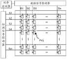
图1为一种硅基OLED显示装置的结构示意图。如图1所示,硅基OLED显示装置可以包括时序控制器、数据信号驱动器、扫描信号驱动器和像素阵列,像素阵列可以包括多个扫描信号线(S1到Sm)、多个数据信号线(D1到Dn)和多个子像素Pxij。在示例性实施方式中,时序控制器可以将适合于数据信号驱动器的规格的灰度值和控制信号提供到数据信号驱动器,可以将适合于扫描信号驱动器的规格的时钟信号、扫描起始信号等提供到扫描信号驱动器。数据信号驱动器可以利用从时序控制器接收的灰度值和控制信号来产生将提供到数据信号线D1、D2、D3、……和Dn的数据电压。例如,数据信号驱动器可以利用时钟信号对灰度值进行采样,并且以子像素行为单位将与灰度值对应的数据电压施加到数据信号线D1至Dn,n可以是自然数。扫描信号驱动器可以通过从时序控制器接收时钟信号、扫描起始信号等来产生将提供到扫描信号线S1、S2、S3、……和Sm的扫描信号。例如,扫描信号驱动器可以将具有导通电平脉冲的扫描信号顺序地提供到扫描信号线S1至Sm。例如,扫描信号驱动器可以被构造为移位寄存器的形式,并且可以以在时钟信号的控制下顺序地将以导通电平脉冲形式提供的扫描起始信号传输到下一级电路的方式产生扫描信号,m可以是自然数。子像素阵列可以包括多个像素子PXij。每个像素子PXij可以连接到对应的数据信号线和对应的扫描信号线,i和j可以是自然数。子像素PXij可以指其中晶体管连接到第i扫描信号线且连接到第j数据信号线的子像素。FIG. 1 is a schematic structural diagram of a silicon-based OLED display device. As shown in FIG. 1, a silicon-based OLED display device may include a timing controller, a data signal driver, a scan signal driver, and a pixel array, and the pixel array may include a plurality of scan signal lines (S1 to Sm), a plurality of data signal lines (D1) to Dn) and multiple sub-pixels Pxij. In an exemplary embodiment, the timing controller may supply a grayscale value and a control signal suitable for the specification of the data signal driver to the data signal driver, and may supply a clock signal, a scan start signal, etc., suitable for the specification of the scan signal driver supplied to the scan signal driver. The data signal driver may generate data voltages to be supplied to the data signal lines D1 , D2 , D3 , . . . and Dn using the grayscale values and control signals received from the timing controller. For example, the data signal driver may sample grayscale values with a clock signal, and apply data voltages corresponding to the grayscale values to the data signal lines D1 to Dn in units of sub-pixel rows, n may be a natural number. The scan signal driver may generate scan signals to be supplied to the scan signal lines S1 , S2 , S3 , . . . and Sm by receiving a clock signal, a scan start signal, and the like from the timing controller. For example, the scan signal driver may sequentially supply scan signals having on-level pulses to the scan signal lines S1 to Sm. For example, the scan signal driver may be constructed in the form of a shift register, and may generate scans in such a manner that a scan start signal supplied in the form of an on-level pulse is sequentially transmitted to the next stage circuit under the control of a clock signal signal, m can be a natural number. The sub-pixel array may include a plurality of pixel sub-PXij. Each pixel sub-PXij may be connected to a corresponding data signal line and a corresponding scan signal line, and i and j may be natural numbers. The sub-pixel PXij may refer to a sub-pixel in which a transistor is connected to the i-th scan signal line and to the j-th data signal line.
图2为一种硅基OLED显示装置中显示区域的平面结构示意图。如图2所示,显示区域可以包括以矩阵方式排布的多个像素单元P,多个像素单元P的至少一个包括出射第一颜色光线的第一子像素P1、出射第二颜色光线的第二子像素P2和出射第三颜色光线的第三子像素P3,第一子像素P1、第二子像素P2和第三子像素P3均包括像素驱动电路和发光器件。子像素中的像素驱动电路分别与扫描信号线和数据信号线连接,像素驱动电路被配置为在扫描信号线的控制下,接收数据信号线传输的数据电压,向显示发光器件输出相应的电流。子像素中的显示发光器件分别与所在子像素的像素驱动电路连接,显示发光器件被配置为响应所在子像素的像素驱动电路输出的电流发出相应亮度的光。FIG. 2 is a schematic plan view of a display area in a silicon-based OLED display device. As shown in FIG. 2 , the display area may include a plurality of pixel units P arranged in a matrix, and at least one of the plurality of pixel units P includes a first sub-pixel P1 that emits light of a first color, and a first sub-pixel P1 that emits light of a second color. The two sub-pixels P2 and the third sub-pixel P3 that emits light of the third color, the first sub-pixel P1, the second sub-pixel P2 and the third sub-pixel P3 all include a pixel driving circuit and a light-emitting device. The pixel driving circuits in the sub-pixels are respectively connected with the scanning signal lines and the data signal lines. The pixel driving circuits are configured to receive data voltages transmitted by the data signal lines under the control of the scanning signal lines, and output corresponding currents to the display light-emitting device. The display light-emitting devices in the sub-pixels are respectively connected with the pixel driving circuits of the sub-pixels, and the display light-emitting devices are configured to emit light with corresponding brightness in response to the current output by the pixel driving circuits of the sub-pixels.
在示例性实施方式中,第一子像素P1可以是出射红色(R)光线的红色子像素、第二子像素P2可以是出射蓝色(B)光线的蓝色子像素,第三子像素P3可以是出射绿色(G)光线的绿色子像素。在示例性实施方式中,子像素的形状可以是三角形、正方形、矩形、菱形、梯形、平行四边形、五边形、六边形和其它多边形中的任意一种或多种,可以采用水平并列、竖直并列、X形、十字形、品字形、正方形、钻石形或者delta等方式排列,本公开在此不做限定。In an exemplary embodiment, the first subpixel P1 may be a red subpixel emitting red (R) light, the second subpixel P2 may be a blue subpixel emitting blue (B) light, and the third subpixel P3 Can be a green sub-pixel that emits green (G) light. In an exemplary embodiment, the shape of the sub-pixels may be any one or more of triangles, squares, rectangles, rhombuses, trapezoids, parallelograms, pentagons, hexagons and other polygons, and horizontal juxtaposition, Vertical juxtaposition, X-shaped, cross-shaped, fret-shaped, square, diamond-shaped, or delta-shaped, etc., are not limited in the present disclosure.
在示例性实施方式中,像素单元可以包括四个子像素,本公开在此不做限定。In an exemplary embodiment, the pixel unit may include four sub-pixels, which is not limited in the present disclosure.
目前Micro-OLED显示面板为了提升亮度,主要通过叠层(tandem)结构实现,然而对于这种结构,由于像素间距离比较近,容易发生串色问题。At present, the Micro-OLED display panel is mainly realized by a tandem structure in order to improve the brightness. However, for this structure, because the distance between the pixels is relatively close, the problem of cross-color is prone to occur.
本公开实施例提供了一种显示基板,包括:衬底基板以及位于衬底基板上的多个子像素,其中:所述子像素包括第一电极、有机发光层和第二电极,所述第一电极包括至少一层导电层,所述有机发光层包括叠层设置的多个不同颜色的发光层以及设置在所述多个不同颜色的发光层之间的电荷产生层;相邻所述子像素的第一电极之间设置有平坦部以及设置在所述平坦部之上的像素定义层,所述像素定义层包括至少一个隔断开口,所述隔断开口包括靠近所述衬底基板一侧的第一表面、远离所述衬底基板一侧的第二表面以及设置在所述第一表面和第二表面之间的第三侧面,所述第三侧面包括至少一个侧凹结构;在垂直于所述显示基板的方向上,所述平坦部远离衬底基板的表面与所述第一电极远离衬底基板的表面之间的高度差(所述平坦部与所述第一电极之间的高度差)小于或等于任意一层所述导电层的厚度。Embodiments of the present disclosure provide a display substrate, including: a base substrate and a plurality of sub-pixels located on the base substrate, wherein: the sub-pixels include a first electrode, an organic light-emitting layer and a second electrode, the first The electrode includes at least one conductive layer, and the organic light-emitting layer includes a plurality of light-emitting layers of different colors arranged in a stack and a charge generation layer arranged between the plurality of light-emitting layers of different colors; adjacent to the sub-pixels A flat portion and a pixel definition layer disposed above the flat portion are arranged between the first electrodes of the two electrodes. a surface, a second surface on the side away from the base substrate, and a third side surface disposed between the first surface and the second surface, the third side surface including at least one undercut structure; In the direction of the display substrate, the height difference between the surface of the flat portion away from the base substrate and the surface of the first electrode away from the base substrate (the height difference between the flat portion and the first electrode ) is less than or equal to the thickness of any one of the conductive layers.
本实施例中,在平行于所述显示基板的方向上,所述电荷产生层在所述侧凹结构的位置处不连续。In this embodiment, in a direction parallel to the display substrate, the charge generation layer is discontinuous at the position of the undercut structure.
本公开实施例的显示基板,通过在子像素之间设置平坦部以及位于平坦部之上的像素定义层,像素定义层包括至少一个隔断开口,隔断开口的侧面设置至少一个侧凹结构,且电荷产生层在侧凹结构的位置处不连续,平坦部与第一电极之间的高度差小于或等于第一电极中任意一层导电层的厚度,从而有效地隔断了相邻子像素之间的电荷产生层,避免了相邻子像素之间产生串扰。In the display substrate of the embodiment of the present disclosure, a flat portion is provided between the sub-pixels and a pixel definition layer located on the flat portion, the pixel definition layer includes at least one partition opening, and at least one undercut structure is provided on the side of the partition opening, and the charge The generation layer is discontinuous at the position of the undercut structure, and the height difference between the flat portion and the first electrode is less than or equal to the thickness of any conductive layer in the first electrode, thereby effectively blocking the connection between adjacent sub-pixels. The charge generation layer avoids crosstalk between adjacent sub-pixels.
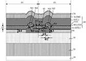
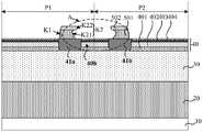
如图3或图4并结合图8d或图11d图所示,显示基板包括:衬底基板10以及位于衬底基板10上的多个子像素;子像素包括第一电极40、有机发光层60和第二电极70,有机发光层60包括叠层设置的多个不同颜色的发光层EML以及设置在多个不同颜色的发光层EML之间的电荷产生层CGL;相邻子像素之间设置有平坦部41以及位于平坦部41之上的像素定义层,像素定义层包括至少一个隔断开口K2,隔断开口K2包括靠近衬底基板10一侧的第一表面K2a、远离衬底基板10一侧的第二表面K2b以及设置在第一表面K2a和第二表面K2b之间的第三侧面K2c,第三侧面K2c包括至少一个侧凹结构,在平行于衬底基板10的方向上,电荷产生层CGL在侧凹结构的位置处不连续。As shown in FIG. 3 or FIG. 4 in combination with FIG. 8d or FIG. 11d , the display substrate includes: a
第一电极40包括至少一层导电层(示例性的,第一电极40可以包括从下至上依次设置的第一钛层、铝层、第二钛层和透明金属氧化物膜层;或者,第一电极40可以包括从下至上依次设置的第一透明金属氧化物膜层、银层和第二透明金属氧化物膜层),在垂直于显示基板的方向上,平坦部41远离衬底基板10的表面与第一电极40远离衬底基板10的表面之间的高度差(即平坦部41与第一电极40之间的高度差(h3-h4))小于或等于任意一层导电层的厚度。The
在示例性实施方式中,平坦部41的高度h3与第一电极40的高度h4之间的差值可以为0±100nm。In an exemplary embodiment, the difference between the height h3 of the
在示例性实施方式中,在垂直于显示基板的方向上,平坦部41远离衬底基板10的表面与第一电极40远离衬底基板10的表面等高齐平。In an exemplary embodiment, in a direction perpendicular to the display substrate, the surface of the
需要说明的是,本公开所述的“等高齐平”不仅仅包括平坦部41的高度h3等于第一电极40的高度h4的情况,还包括两者之间近似相等的情况,即允许两者之间存在一定的误差范围,示例性的,该误差范围可以是在0um到50nm之间。It should be noted that the “equal-height flush” mentioned in the present disclosure not only includes the case where the height h3 of the
在示例性实施方式中,像素定义层在衬底基板10上的正投影位于平坦部41在衬底基板10上的正投影之内。In an exemplary embodiment, the orthographic projection of the pixel definition layer on the
本公开实施例的显示基板,由于像素定义层在衬底基板10上的正投影位于平坦部41在衬底基板10上的正投影之内,这样,第一电极40靠近平坦部41的上边缘距离第二电极坡面上任一点的距离等于或者近似等于第一电极40与第二电极70之间的高度差,从而可以降低第二电极穿刺的影响。In the display substrate of the embodiment of the present disclosure, since the orthographic projection of the pixel definition layer on the
在示例性实施方式中,平坦部41在衬底基板10上的正投影与第一电极40在衬底基板10上的正投影不交叠。In the exemplary embodiment, the orthographic projection of the
本公开实施例的显示基板,由于平坦部41在衬底基板10上的正投影与第一电极40在衬底基板10上的正投影不交叠,因此,在防止相邻子像素之间产生串扰的同时,还能够提高开口率。In the display substrate of the embodiment of the present disclosure, since the orthographic projection of the
在示例性实施方式中,在垂直于该衬底基板10的方向上,电荷产生层CGL远离衬底基板10的表面与第一电极40远离衬底基板10的表面之间的距离,小于或等于侧凹结构的高度(即,侧凹结构的高度h1大于或等于电荷产生层CGL与第一电极40之间的高度差h2)。In the exemplary embodiment, in the direction perpendicular to the
在示例性实施方式中,如图3所示,平坦部41包括第一平坦部41a、第二平坦部41b以及位于第一平坦部41a与第二平坦部41b之间的隔断电极40b。In an exemplary embodiment, as shown in FIG. 3 , the
本公开通过设置第一平坦部41a、第二平坦部41b以及位于第一平坦部41a与第二平坦部41b之间的隔断电极40b,可以控制第二电极穿刺与第一电极之间的距离,从而可以有效解决第二电极穿刺引起有机发光层周边亮度不均匀的问题。In the present disclosure, by providing the first
在示例性实施方式中,如图3所示,隔断开口K2在衬底基板10上的正投影与隔断电极40b在衬底基板10上的正投影存在重叠区域。In the exemplary embodiment, as shown in FIG. 3 , the orthographic projection of the partition opening K2 on the
在示例性实施方式中,如图3和图7所示,沿平行于显示基板的方向,第一平坦部41a的宽度w1与第二平坦部41b的宽度w3相等或近似相等,隔断电极40b的宽度w2为第一平坦部41a的宽度w1的1倍到2倍之间。示例性的,第一平坦部41a的宽度w1可以大于或等于0.2um。第二平坦部41b的宽度w3可以大于或等于0.2um。隔断电极40b的宽度w2可以大于或等于0.2um。In the exemplary embodiment, as shown in FIGS. 3 and 7 , along a direction parallel to the display substrate, the width w1 of the first
在示例性实施方式中,如图3所示,在垂直于显示基板的方向上,第一平坦部41a远离衬底基板10的表面、第二平坦部41b远离衬底基板10的表面与第一电极40远离衬底基板10的表面等高齐平。即,第一平坦部41a的高度h31以及第二平坦部41b的高度h32等于第一电极40的高度h4。In an exemplary embodiment, as shown in FIG. 3 , in a direction perpendicular to the display substrate, the first
在示例性实施方式中,如图3和图8c所示,像素定义层包括从下至上依次叠层设置的第一像素定义层501和第二像素定义层502,其中:In an exemplary embodiment, as shown in FIG. 3 and FIG. 8 c , the pixel definition layer includes a first
第一像素定义层501包括第一子隔断开口K21,第二像素定义层502包括第二子隔断开口K22,第一子隔断开口K21和第二子隔断开口K22贯通形成隔断开口K2,且第一子隔断开口K21在衬底基板10上的正投影大于第二子隔断开口K22在衬底基板上的正投影,第一子隔断开口K21和第二子隔断开口K22形成侧凹结构。The first
为了形成侧凹结构,可以通过调控像素定义层之间的刻蚀速率实现,示例性的,使用刻蚀速率不同的材料分别构成第一像素定义层501和第二像素定义层502。其中,第一像素定义层501的刻蚀速率大于第二像素定义层502的刻蚀速率。In order to form the undercut structure, it can be achieved by adjusting the etching rate between the pixel definition layers. Exemplarily, materials with different etching rates are used to form the first
在示例性实施方式中,第一像素定义层501的材料为硅氮化物SiNx,第二像素定义层502的材料为硅氧化物SiOx;或者,第一像素定义层501的材料为硅氮化物SiNx,第二像素定义层502的材料为氧化铝Al2O3。In an exemplary embodiment, the material of the first
在示例性实施方式中,平坦部41在衬底基板10上的正投影与第一电极40在衬底基板上的正投影不交叠,以增大开口率。In the exemplary embodiment, the orthographic projection of the
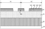
在示例性实施方式中,如图4所示,第一电极40包括多个子第一电极块,平坦部41设置在相邻两个子第一电极块之间。In an exemplary embodiment, as shown in FIG. 4 , the
在示例性实施方式中,第一电极40包括从下至上依次设置的第一子电极层401、第二子电极层402、第三子电极层403和第四子电极层404。在示例性实施方式中,第一子电极层401的材料可以为钛,第二子电极层402的材料可以为铝,第三子电极层403的材料可以为钛,第四子电极层404的材料可以为金属氧化物。In an exemplary embodiment, the
在示例性实施方式中,第一电极40包括从下至上依次设置的第一子电极层401、第二子电极层402和第三子电极层403。在示例性实施方式中,第一子电极层401的材料可以为金属氧化物,第二子电极402的材料可以为银,第三子电极层403的材料可以为金属氧化物。In an exemplary embodiment, the
下面通过显示基板的制备过程进行示例性说明。本公开所说的“图案化工艺”,对于金属材料、无机材料或透明导电材料,包括涂覆光刻胶、掩模曝光、显影、刻蚀、剥离光刻胶等处理,对于有机材料,包括涂覆有机材料、掩模曝光和显影等处理。沉积可以采用溅射、蒸镀、化学气相沉积中的任意一种或多种,涂覆可以采用喷涂、旋涂和喷墨打印中的任意一种或多种,刻蚀可以采用干刻和湿刻中的任意一种或多种,本公开不做限定。“薄膜”是指将某一种材料在基底上利用沉积、涂覆或其它工艺制作出的一层薄膜。若在整个制作过程当中该“薄膜”无需图案化工艺,则该“薄膜”还可以称为“层”。若在整个制作过程当中该“薄膜”需图案化工艺,则在图案化工艺前称为“薄膜”,图案化工艺后称为“层”。经过图案化工艺后的“层”中包含至少一个“图案”。本公开所说的“A和B同层设置”是指,A和B通过同一次图案化工艺同时形成,膜层的“厚度”为膜层在垂直于显示装置方向上的尺寸。本公开示例性实施例中,“B的正投影位于A的正投影的范围之内”或者“A的正投影包含B的正投影”是指,B的正投影的边界落入A的正投影的边界范围内,或者A的正投影的边界与B的正投影的边界重叠。The following is an exemplary description through the preparation process of the display substrate. The "patterning process" mentioned in this disclosure, for metal materials, inorganic materials or transparent conductive materials, includes photoresist coating, mask exposure, development, etching, stripping photoresist and other treatments, for organic materials, including Processes such as coating organic materials, mask exposure and development. Deposition can use any one or more of sputtering, evaporation, chemical vapor deposition, coating can use any one or more of spraying, spin coating and inkjet printing, etching can use dry etching and wet Any one or more of the engravings are not limited in the present disclosure. "Film" refers to a thin film made of a material on a substrate by deposition, coating or other processes. If the "thin film" does not require a patterning process during the entire fabrication process, the "thin film" may also be referred to as a "layer". If the "thin film" needs a patterning process in the whole manufacturing process, it is called a "thin film" before the patterning process, and a "layer" after the patterning process. The "layer" after the patterning process contains at least one "pattern". In the present disclosure, "A and B are arranged in the same layer" means that A and B are simultaneously formed through the same patterning process, and the "thickness" of the film layer is the dimension of the film layer in the direction perpendicular to the display device. In an exemplary embodiment of the present disclosure, “the orthographic projection of B is within the range of the orthographic projection of A” or “the orthographic projection of A includes the orthographic projection of B” means that the boundary of the orthographic projection of B falls within the orthographic projection of A or the boundary of the orthographic projection of A overlaps the boundary of the orthographic projection of B.
在示例性实施方式中,图3所示的显示基板的制备过程可以包括如下步骤:In an exemplary embodiment, the preparation process of the display substrate shown in FIG. 3 may include the following steps:
(11)形成衬底基板10,示例性的,衬底基板10可以为硅基衬底。形成衬底基板10的制程可以采用相关技术成熟的IC(Intergrated Circuit)晶片制程,这里不再赘述。(11) Forming the
(12)形成驱动电路层20。驱动电路层20可以通过硅半导体工艺(例如互补金属氧化物半导体(Complementary Metal Oxide Semiconductor,CMOS)工艺)制备在衬底基板10上,驱动电路层20可以包括多个电路单元,电路单元可以至少包括像素驱动电路,像素驱动电路分别与扫描信号线和数据信号线连接,像素驱动电路可以包括多个晶体管和存储电容,晶体管可以包括控制极、第一极和第二极,控制极、第一极和第二极可以通过钨金属填充的过孔(即钨过孔,W-via)分别与相应的连接电极连接,并可以通过连接电极与其它电学结构(如走线等)进行连接。(12) The
(13)形成第一绝缘层30。在示例性实施方式中,形成第一绝缘层30图案包括:在形成前述图案的衬底基板上沉积第一绝缘薄膜,通过构图工艺对第一绝缘薄膜进行构图,形成覆盖驱动电路层20的第一绝缘层30图案,如图5所示。(13) The first insulating
(14)形成第一电极40和隔断电极40b。在示例性实施方式中,形成第一电极40和隔断电极40b图案包括:在形成前述图案的衬底基板上沉积第一电极材料薄膜,通过图案化工艺对第一电极材料薄膜进行图案化,形成设置在第一绝缘层30上的第一电极40和隔断电极40b图案,如图6所示。(14) The
在一些示例性实施方式中,第一电极40和隔断电极40b的材料可以采用金属或金属氧化物。In some exemplary embodiments, the material of the
在一些示例性实施方式中,第一电极40和隔断电极40b可以为叠层结构。In some exemplary embodiments, the
可选的,如图6所示,第一电极40和隔断电极40b可以包括金属膜层以及位于金属膜层上方的透明金属氧化物膜层404。金属膜层可以包括依次层叠设置在第一绝缘层30上的第一钛层401、铝层402和第二钛层403;透明金属氧化物膜层404可以采用氧化铟锡(ITO)或氧化铟锌(IZO)。Optionally, as shown in FIG. 6 , the
可选的,第一电极40和隔断电极40b可以包括两层透明金属氧化物膜层及位于两层透明金属氧化物膜层之间的金属膜层(图中未示出),透明金属氧化物膜层的材料可以是氧化铟锡(ITO)或氧化铟锌(IZO),金属膜层的材料可以是金属银。Optionally, the
在一些示例性实施方式中,第一电极40和隔断电极40b可以间隔设置,第一电极40与后续形成的有机发光层60连接,隔断电极40b与后续形成的第一平坦部41a、第二平坦部41b、像素定义层形成隔断部。In some exemplary embodiments, the
(15)形成第一平坦部和第二平坦部。在示例性实施方式中,形成第一平坦部和第二平坦部图案包括:在形成前述图案的衬底基板上,沉积第一平坦薄膜,采用图案化工艺对第一平坦薄膜进行图案化,形成设置在第一绝缘层30上的第一平坦部41a和第二平坦部41b图案,如图7所示。(15) A first flat portion and a second flat portion are formed. In an exemplary embodiment, forming the patterns of the first flat portion and the second flat portion includes: depositing a first flat film on the base substrate on which the aforementioned patterns are formed, patterning the first flat film by a patterning process, and forming The patterns of the first
在一些示例性实施方式中,第一平坦部41a和第二平坦部41b设置于第一电极40和隔断电极40b之间的间隔区域,且第一平坦部41a和第二平坦部41b填满第一电极40和隔断电极40b之间的间隔区域。沿垂直于衬底基板10的方向,第一平坦部41a和第二平坦部41b的高度与第一电极40的高度相同(即,第一平坦部41a远离衬底基板10的表面、第二平坦部41b远离衬底基板10的表面以及第一电极40远离衬底基板10的表面等高齐平)。In some exemplary embodiments, the first
(16)形成像素定义层。在示例性实施方式中,形成像素定义层图案包括如下步骤:(16) A pixel definition layer is formed. In an exemplary embodiment, forming a pixel definition layer pattern includes the steps of:
在形成前述图案的衬底基板上涂覆多层像素定义薄膜,多层像素定义薄膜至少包括第一像素定义薄膜501以及位于第一像素定义薄膜501之上的第二像素定义薄膜502,如图8a所示。在示例性实施例中,多层薄膜可以包括从下至上依次叠层设置的第一像素定义薄膜、第二像素定义薄膜、第三像素定义薄膜和第四像素定义薄膜。本公开实施例中,相邻两层像素定义薄膜需要选用刻蚀速率比差异较大的材料,示例性的,沿远离衬底基板的方向,第(2n-1)层像素定义薄膜可以为硅氮化物SiNx薄膜,第(2n)层像素定义薄膜可以为硅氧化物SiOx薄膜(SiNx薄膜的刻蚀速率大于SiOx薄膜的刻蚀速率);或者,第(2n-1)层像素定义薄膜可以为硅氮化物SiNx薄膜,第(2n)层像素定义薄膜可以为氧化铝al2O3薄膜(SiNx薄膜的刻蚀速率大于氧化铝Al2O3薄膜的刻蚀速率),n为大于或等于1的自然数。在另一些示例性实施例中,相邻两层像素定义薄膜也可以采用其他刻蚀速率比差异较大的材料,本公开对此不作限制。在另一些示例性实施例中,多层薄膜也可以包括两层、五层、六层等其他两层以上的任意层数,本公开对此不作限制;A multi-layer pixel-defining film is coated on the base substrate formed with the aforementioned pattern, and the multi-layer pixel-defining film at least includes a first pixel-defining
对位于第一电极40上方的多层像素定义薄膜进行刻蚀,形成像素开口K1,如图8b所示,像素开口K1暴露出至少部分第一电极40;etching the multi-layer pixel definition film above the
对位于第一平坦部41a、第二平坦部41b和隔断电极40b上方的多层像素定义薄膜进行刻蚀,使每一层像素定义薄膜形成一个子隔断开口,多个子隔断开口形成总的隔断开口K2,其中,由于进行刻蚀时,沿远离衬底基板的方向,第(2n-1)层像素定义薄膜的刻蚀速率大于第(2n)层像素定义薄膜的刻蚀速率,因此,第(2n-1)层像素定义薄膜的子隔断开口大于第(2n)层像素定义薄膜的子隔断开口,如图8c和图8d所示。示例性的,第一像素定义薄膜501形成第一子隔断开口K21,第二像素定义薄膜502形成第二子隔断开口K22,且第一子隔断开口K21大于第二子隔断开口K22,第一子隔断开口K21和第二子隔断开口K22形成一个侧凹结构。The multi-layer pixel definition films located above the first
可选地,可以采用干法刻蚀对位于第一平坦部41a、第二平坦部41b和隔断电极40b上方的多层像素定义层薄膜进行刻蚀,因第(2n-1)层像素定义薄膜相对于第(2n)层像素定义薄膜的刻蚀速率要快的多,因此,同样刻蚀条件下,第(2n-1)层像素定义薄膜的开口大于第(2n)层像素定义薄膜的开口,这里的干法刻蚀包括但不限于溅射与离子束铣蚀、等离子刻蚀、高压等离子刻蚀、高密度等离子体刻蚀和反应离子刻蚀。Optionally, dry etching may be used to etch the multilayer pixel definition layer films located above the first
可选地,也可以采用湿法刻蚀对位于第一平坦部41a、第二平坦部41b和隔断电极40b上方的多层像素定义层薄膜进行刻蚀,且选择使用对第(2n-1)层像素定义薄膜的刻蚀速率比对第(2n)层像素定义薄膜的刻蚀速率大的刻蚀液。Optionally, wet etching can also be used to etch the multilayer pixel definition layer film located above the first
在一些示例性实施方式中,像素定义层在衬底基板10上的正投影与第一平坦部41a和第二平坦部41b在衬底基板10上的正投影存在重叠区域,隔断开口K2在衬底基板10上的正投影与隔断电极40b在衬底基板10上的正投影存在重叠区域。In some exemplary embodiments, the orthographic projection of the pixel definition layer on the
在一些示例性实施方式中,像素定义层在衬底基板10上的正投影与第一电极40在衬底基板上的正投影不交叠,以提升开口率。In some exemplary embodiments, the orthographic projection of the pixel definition layer on the
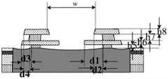
在示例性实施方式中,如图8d所示,沿垂直于显示基板的方向,第二像素定义薄膜502的厚度h6是第一像素定义薄膜501的厚度h5的0.4倍到3倍之间。In an exemplary embodiment, as shown in FIG. 8d, the thickness h6 of the second
示例性的,如图8d所示,第二像素定义薄膜502的厚度h6为400埃米至1500埃米之间,第一像素定义薄膜501的厚度h5为300埃米至1000埃米之间。Exemplarily, as shown in FIG. 8d , the thickness h6 of the second
在示例性实施方式中,如图8d所示,沿平行于显示基板的方向,第一子隔断开口K21的边缘与第二子隔断开口K22的边缘之间的距离d1为第一子隔断开口K21的宽度w的0.1倍到1.5倍之间。In an exemplary embodiment, as shown in FIG. 8d, along the direction parallel to the display substrate, the distance d1 between the edge of the first sub-partition opening K21 and the edge of the second sub-partition opening K22 is the first sub-partition opening K21 is between 0.1 and 1.5 times the width w.
在示例性实施方式中,如图8d所示,沿平行于显示基板的方向,第一子隔断开口K21的边缘与第二子隔断开口K22的边缘之间的距离d1为0.1微米到0.6微米之间。In an exemplary embodiment, as shown in FIG. 8d, along a direction parallel to the display substrate, the distance d1 between the edge of the first sub-partition opening K21 and the edge of the second sub-partition opening K22 is between 0.1 μm and 0.6 μm between.
在示例性实施方式中,如图8d所示,在实现隔断的前提下,尽量缩短第一子隔断开口K21的宽度,以提高显示面板的分辨率以及开口率。示例性地,沿平行于显示基板的方向,第一子隔断开口K21的宽度w为0.4微米到1微米之间。In an exemplary embodiment, as shown in FIG. 8d , on the premise of realizing the partition, the width of the first sub-partition opening K21 is shortened as much as possible to improve the resolution and aperture ratio of the display panel. Exemplarily, along a direction parallel to the display substrate, the width w of the first sub-isolation opening K21 is between 0.4 micrometer and 1 micrometer.
在一些示例性实施方式中,隔断开口K2在衬底基板10上的正投影包含隔断电极40b在衬底基板10上的正投影,即隔断电极40b在衬底基板10上的正投影落在隔断开口K2在衬底基板10上的正投影的范围之内。In some exemplary embodiments, the orthographic projection of the isolation opening K2 on the
示例性的,当像素定义层包括第一像素定义层至第四像素定义层四层时,第一像素定义薄膜的厚度可以大于第三像素定义薄膜的厚度,第一像素定义薄膜的厚度也可以小于第三像素定义薄膜的厚度,本公开对此不作限定。本实施例中,第一像素定义薄膜的厚度和第三像素定义薄膜的厚度根据第二像素定义薄膜的厚度与第四像素定义薄膜的厚度进行设定。由于侧凹结构的高度大于或等于电荷产生层与第一电极之间的高度差,因此,第一像素定义薄膜的厚度和第三像素定义薄膜的厚度之和大于或等于电荷产生层与第一电极之间的高度差与第二像素定义薄膜的厚度及第四像素定义薄膜的厚度之差,以使得隔断结构能够隔断CGL层(当CGL层包含多层时,本申请的隔断结构也能隔断所有的CGL层),从而防止相邻子像素之间产生串扰。Exemplarily, when the pixel definition layer includes four layers from the first pixel definition layer to the fourth pixel definition layer, the thickness of the first pixel definition film may be greater than the thickness of the third pixel definition film, and the thickness of the first pixel definition film may also be It is less than the thickness of the third pixel-defining film, which is not limited in the present disclosure. In this embodiment, the thickness of the first pixel definition film and the thickness of the third pixel definition film are set according to the thickness of the second pixel definition film and the thickness of the fourth pixel definition film. Since the height of the undercut structure is greater than or equal to the height difference between the charge generation layer and the first electrode, the sum of the thickness of the first pixel definition film and the thickness of the third pixel definition film is greater than or equal to the charge generation layer and the first electrode. The height difference between the electrodes and the difference between the thickness of the second pixel definition film and the thickness of the fourth pixel definition film, so that the partition structure can partition the CGL layer (when the CGL layer includes multiple layers, the partition structure of the present application can also partition all CGL layers), thereby preventing crosstalk between adjacent sub-pixels.
示例性的,第一像素定义薄膜的厚度大于第二像素定义薄膜的厚度,第三像素定义薄膜的厚度大于第四像素定义薄膜的厚度,以提高侧凹结构的高度,使得隔断部能够更好的起到防串扰的作用,但是,本公开对此并不做限定。Exemplarily, the thickness of the first pixel-defining film is greater than the thickness of the second pixel-defining film, and the thickness of the third pixel-defining film is greater than the thickness of the fourth pixel-defining film, so as to increase the height of the undercut structure, so that the partition can be better It plays the role of anti-crosstalk, but this disclosure does not limit it.
(17)形成有机发光层60和第二电极70图案。(17) Patterning the organic light-emitting
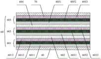
图9a为本公开有机发光层60的一种结构示意图。如图9a所示,本公开有机发光层的结构包括在第一电极40与第二电极70之间依次叠设的第一发光子层601、第一电荷产生层602、第二发光子层603、第二电荷产生层604和第三发光子层605。第一发光子层601用于出射第一颜色光,包括依次叠设的第一空穴传输层(HTL)6011、第一发光材料层(EML)6012和第一电子传输层(ETL)6013。第二发光子层603用于出射第二颜色光,包括依次叠设的第二空穴传输层6031、第二发光材料层6032和第二电子传输层6033。第三发光子层605用于出射第三颜色光,包括依次叠设的第三空穴传输层6051、第三发光材料层6052和第三电子传输层6053。第一电荷产生层602设置在第一发光子层601与第二发光子层603之间,用于将两个发光子层串联起来,实现载流子的传递。第二电荷产生层604设置在第二发光子层603与第三发光子层605之间,用于将两个发光子层串联起来,实现载流子的传递。由于本公开有机发光层包括出射第一颜色光的第一发光材料层、出射第二颜色光的第二发光材料层和出射第三颜色光的第三发光材料层,因而有机发光层最终出射的光为混合光。例如,可以设置第一发光材料层是出射红光的红光材料层,第二发光材料层是出射绿光的绿光材料层,第三发光材料层是出射蓝光的红光材料层,因而有机发光层最终出射白光。FIG. 9a is a schematic structural diagram of an organic light-emitting
在示例性实施方式中,图9a所示的有机发光层仅仅是一种示例结构,本公开对此不作限制。实际实施时,可以根据实际需要设计有机发光层的结构。例如,每个发光子层中,为了能够提高电子和空穴注入发光材料层的效率,还可以设置空穴注入层(HIL)和电子注入层(EIL)。又如,为了简化有机发光层的结构,可以取消第一电子传输层6013、第一电荷产生层602和第二空穴传输层6031,即第二发光材料层6032直接设置在第一发光材料层6012上,如图9b所示。In the exemplary embodiment, the organic light-emitting layer shown in FIG. 9a is only an exemplary structure, which is not limited by the present disclosure. In actual implementation, the structure of the organic light-emitting layer can be designed according to actual needs. For example, in each light-emitting sublayer, in order to improve the efficiency of electron and hole injection into the light-emitting material layer, a hole injection layer (HIL) and an electron injection layer (EIL) may also be provided. For another example, in order to simplify the structure of the organic light-emitting layer, the first
在一些可能的实现方式中,有机发光层可以采用出射第一颜色光的有机发光层和出射第一颜色光的互补光的有机发光层,该两个有机发光层相对于衬底基板依次堆叠,从而整体上发白光,本公开对此不作限制,只要可以实现发白光即可。In some possible implementations, the organic light-emitting layer may adopt an organic light-emitting layer that emits light of the first color and an organic light-emitting layer that emits complementary light of the first color, and the two organic light-emitting layers are stacked in sequence relative to the base substrate, Therefore, white light is emitted as a whole, which is not limited in the present disclosure, as long as white light can be emitted.
为了更清楚看出电荷产生层(CGL)是否产生膜层断裂,如图3所示,我们把有机发光层简单划分为5层,分别为第一空穴传输层(HTL1)、红绿发光材料层(RG-EML)、电荷产生层(CGL)、第二空穴传输层(HTL2)和蓝色发光材料层(B-EML)。从图3所示的这五层在在形成前述图案的衬底基板上的沉积结果可以看出,电荷产生层(CGL)在像素定义层的侧凹结构处发生了膜层断裂,从而使得相邻子像素之间不会产生串扰,同时,本实施例的显示基板还降低了第一电极边缘处上方的第二电极形貌穿刺问题,提高了显示效果。此外,本公开的制备工艺可以很好地与现有制备工艺兼容,工艺实现简单,易于实施,生产效率高,生产成本低,良品率高。In order to clearly see whether the charge generation layer (CGL) has film breakage, as shown in Figure 3, we simply divide the organic light-emitting layer into five layers, namely the first hole transport layer (HTL1), the red and green light-emitting materials layer (RG-EML), charge generation layer (CGL), second hole transport layer (HTL2) and blue light emitting material layer (B-EML). It can be seen from the deposition results of the five layers shown in FIG. 3 on the base substrate on which the aforementioned patterns are formed that the charge-generating layer (CGL) is fractured at the undercut structure of the pixel definition layer, thereby causing the phase There is no crosstalk between adjacent sub-pixels, and at the same time, the display substrate of this embodiment also reduces the problem of puncturing the topography of the second electrode above the edge of the first electrode, thereby improving the display effect. In addition, the preparation process of the present disclosure can be well compatible with the existing preparation process, and the process is simple to realize, easy to implement, high in production efficiency, low in production cost and high in yield.
在一些示例性实施方式中,后续制备流程可以包括:形成第一封装层、彩膜结构层、第二封装层和盖板层等工艺。In some exemplary embodiments, the subsequent preparation process may include processes such as forming a first encapsulation layer, a color filter structure layer, a second encapsulation layer, and a cover layer.
在示例性实施方式中,第一封装层和第二封装层可以采用薄膜封装(Thin FilmEncapsulation,简称TFE)方式,可以保证外界水汽无法进入发光结构层,盖板层可以采用玻璃,或者采用塑胶类无色聚酰亚胺等。In an exemplary embodiment, the first encapsulation layer and the second encapsulation layer may adopt a thin film encapsulation (TFE for short) method, which can ensure that external water vapor cannot enter the light emitting structure layer, and the cover layer may be made of glass or plastic. Colorless polyimide, etc.
在示例性实施方式中,彩膜结构层可以包括黑矩阵(BM)和彩色滤光片(CF),彩色滤光片的位置可以与发光器件的位置相对应,黑矩阵可以位于相邻的彩色滤光片之间,彩色滤光片被配置为将发光器件出射的白光过滤成红色(R)光、绿色(G)光和蓝色(B)光,形成红色子像素、绿色子像素和蓝色子像素。In an exemplary embodiment, the color filter structure layer may include a black matrix (BM) and a color filter (CF), the position of the color filter may correspond to the position of the light emitting device, and the black matrix may be located in an adjacent color filter Between the filters, the color filters are configured to filter the white light emitted from the light emitting device into red (R) light, green (G) light and blue (B) light, forming red sub-pixels, green sub-pixels and blue light Color sub-pixels.
在示例性实施方式中,图4所示的显示基板的制备过程可以包括如下步骤:In an exemplary embodiment, the manufacturing process of the display substrate shown in FIG. 4 may include the following steps:
(21)形成衬底基板10。示例性的,衬底基板可以为硅基衬底。(21) The
(22)形成驱动电路层20。(22) The
(23)形成第一绝缘层30。步骤(21)至(23)的制备过程可参考前述步骤(11)至(13),此处不再赘述。(23) The first insulating
(24)形成第一电极40。在示例性实施方式中,形成第一电极40图案包括:在形成前述图案的衬底基板上沉积第一电极材料薄膜,通过图案化工艺对第一电极材料薄膜进行图案化,形成设置在第一绝缘层30上的第一电极40图案,如图10a所示。(24) The
在一些示例性实施方式中,第一电极可以包括多个间隔排布的子第一电极块。In some exemplary embodiments, the first electrode may include a plurality of sub-first electrode blocks arranged at intervals.
在一些示例性实施方式中,子第一电极块的材料可以采用金属或金属氧化物。In some exemplary embodiments, the material of the sub-first electrode block may be metal or metal oxide.
在一些示例性实施方式中,子第一电极块可以为叠层结构。In some exemplary embodiments, the sub-first electrode blocks may have a stacked structure.
在一些示例性实施方式中,如图10a所示,子第一电极块可以包括金属膜层以及位于金属膜层上方的透明金属氧化物膜层404。金属膜层可以包括依次层叠设置在第一绝缘层30上的第一钛层401、铝层402和第二钛层403;透明金属氧化物膜层404可以采用氧化铟锡(ITO)或氧化铟锌(IZO)。In some exemplary embodiments, as shown in FIG. 10a, the sub-first electrode block may include a metal film layer and a transparent metal
在另一些示例性实施方式中,子第一电极块可以包括两层透明金属氧化物膜层及位于两层透明金属氧化物膜层之间的金属膜层(图中未示出),透明金属氧化物膜层的材料可以是氧化铟锡(ITO)或氧化铟锌(IZO),金属膜层的材料可以是金属银。In other exemplary embodiments, the sub-first electrode block may include two transparent metal oxide film layers and a metal film layer (not shown in the figure) located between the two transparent metal oxide film layers. The material of the oxide film layer may be indium tin oxide (ITO) or indium zinc oxide (IZO), and the material of the metal film layer may be metallic silver.
(25)形成平坦部41。在示例性实施方式中,形成平坦部41图案包括:在形成前述图案的衬底基板上,沉积第一平坦薄膜,采用图案化工艺对第一平坦薄膜进行图案化,形成设置在第一绝缘层30上的平坦部41图案,如图10b所示。(25) The
在一些示例性实施方式中,平坦部41设置于相邻子像素的子第一电极块之间,平坦部41填满相邻子第一电极块之间的间隔区域,且沿垂直于衬底基板10的方向,平坦部41的高度与相邻子第一电极块的高度相同。In some exemplary embodiments, the
(26)形成像素定义层。在示例性实施方式中,形成像素定义层图案包括如下步骤:(26) A pixel definition layer is formed. In an exemplary embodiment, forming a pixel definition layer pattern includes the steps of:
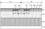
在形成前述图案的衬底基板上涂覆多层薄膜,多层薄膜至少包括第一像素定义薄膜以及位于第一像素定义薄膜之上的第二像素定义薄膜,在示例性实施例中,多层薄膜可以包括从下至上依次叠层设置的第一像素定义薄膜501、第二像素定义薄膜502、第三像素定义薄膜503和第四像素定义薄膜504,如图11a所示。本公开实施例中,相邻两层像素定义薄膜需要选用刻蚀速率比差异较大的材料,示例性的,沿远离衬底基板的方向,第(2n-1)层像素定义薄膜可以为硅氮化物SiNx薄膜,第(2n)层像素定义薄膜可以为硅氧化物SiOx薄膜(SiNx薄膜的刻蚀速率大于SiOx薄膜的刻蚀速率);或者,第(2n-1)层像素定义薄膜可以为硅氮化物SiNx薄膜,第(2n)层像素定义薄膜可以为氧化铝al2O3薄膜(SiNx薄膜的刻蚀速率大于氧化铝Al2O3薄膜的刻蚀速率),n为大于或等于1的自然数。在另一些示例性实施例中,相邻两层像素定义薄膜也可以采用其他刻蚀速率比差异较大的材料,本公开对此不作限制。在另一些示例性实施例中,多层薄膜也可以包括两层、五层、六层等其他两层以上的任意层数,本公开对此不作限制;A multi-layer film is coated on the base substrate formed with the aforementioned pattern, and the multi-layer film includes at least a first pixel-defining film and a second pixel-defining film located on the first pixel-defining film. In an exemplary embodiment, the multi-layer film is The film may include a first
对位于第一电极上方的除第一像素定义薄膜501以外的多层薄膜(即对第二像素定义薄膜502至第四像素定义薄膜504)进行刻蚀,形成子像素开口K1,如图11b所示,子像素开口K1暴露出第一电极40;The multi-layer films (ie, the second
对位于平坦部41上方的多层像素定义薄膜进行刻蚀,使每一层像素定义薄膜形成一个子隔断开口,多个子隔断开口形成总的隔断开口K2,其中,由于进行刻蚀时,沿远离衬底基板的方向,第(2n-1)层像素定义薄膜的刻蚀速率大于第(2n)层像素定义薄膜的刻蚀速率,因此,第(2n-1)层像素定义薄膜的子隔断开口大于第(2n)层像素定义薄膜的子隔断开口,如图11c和图11d所示。示例性的,第一像素定义薄膜501形成第一子隔断开口K21,第二像素定义薄膜502形成第二子隔断开口K22,第三像素定义薄膜503形成第三子隔断开口K23,第四像素定义薄膜504形成第四子隔断开口K24,且第一子隔断开口K21大于第二子隔断开口K22,第三子隔断开口K23大于第四子隔断开口K24,从而使得每两个叠设的像素定义层分别形成一个侧凹结构。The multi-layer pixel-defining films located above the
在示例性实施方式中,如图11d所示,沿平行于显示基板的方向,第一子隔断开口K21的边缘与第二子隔断开口K22的边缘之间的距离d1为第一子隔断开口K21的宽度w的0.1倍到1.5倍之间。In an exemplary embodiment, as shown in FIG. 11d , along a direction parallel to the display substrate, the distance d1 between the edge of the first sub-partition opening K21 and the edge of the second sub-partition opening K22 is the first sub-partition opening K21 is between 0.1 and 1.5 times the width w.
在示例性实施方式中,如图11d所示,沿平行于显示基板的方向,第一子隔断开口K21的边缘与第二子隔断开口K22的边缘之间的距离d1为0.1微米到0.6微米之间。In an exemplary embodiment, as shown in FIG. 11d , along a direction parallel to the display substrate, the distance d1 between the edge of the first sub-partition opening K21 and the edge of the second sub-partition opening K22 is between 0.1 μm and 0.6 μm between.
在示例性实施方式中,如图11d所示,沿平行于显示基板的方向,第三子隔断开口K23的边缘与第四子隔断开口K24的边缘之间的距离d2为第一子隔断开口K21的宽度w的0.1倍到1.5倍之间。In an exemplary embodiment, as shown in FIG. 11d, along a direction parallel to the display substrate, the distance d2 between the edge of the third sub-partition opening K23 and the edge of the fourth sub-partition opening K24 is the first sub-partition opening K21 is between 0.1 and 1.5 times the width w.
在示例性实施方式中,如图11d所示,沿平行于显示基板的方向,第三子隔断开口K23的边缘与第四子隔断开口K24的边缘之间的距离d2为0.1微米到0.6微米之间。In an exemplary embodiment, as shown in FIG. 11d , along a direction parallel to the display substrate, the distance d2 between the edge of the third sub-partition opening K23 and the edge of the fourth sub-partition opening K24 is between 0.1 μm and 0.6 μm between.
在示例性实施方式中,如图11d所示,沿平行于显示基板的方向,第一子隔断开口K21的宽度w为0.4微米到1微米之间。In an exemplary embodiment, as shown in FIG. 11d , along a direction parallel to the display substrate, the width w of the first sub-isolation opening K21 is between 0.4 μm and 1 μm.
示例性的,如图11d所示,第二像素定义薄膜502的厚度h6为200埃米到600埃米之间,第四像素定义薄膜504的厚度h8为200埃米到600埃米之间。Exemplarily, as shown in FIG. 11d , the thickness h6 of the second pixel-defining
示例性的,如图11d所示,第一像素定义薄膜501的厚度h5可以大于第三像素定义薄膜503的厚度h7,第一像素定义薄膜501的厚度h5也可以小于第三像素定义薄膜503的厚度h7。本实施例中,第一像素定义薄膜501的厚度h5和第三像素定义薄膜503的厚度h7根据第二像素定义薄膜502的厚度h6与第四像素定义薄膜504的厚度h8进行设定。由于侧凹结构的高度大于或等于电荷产生层与第一电极之间的高度差,因此,第一像素定义薄膜501的厚度h5和第三像素定义薄膜503的厚度h7之和大于或等于电荷产生层与第一电极之间的高度差与第二像素定义薄膜502的厚度h6及第四像素定义薄膜504的厚度h8之差。Exemplarily, as shown in FIG. 11d , the thickness h5 of the first
另外,在示例性实施方式中,当像素定义层只包括第一像素定义层和第二像素定义层时,沿垂直于显示基板的方向,第二像素定义薄膜502的厚度h6可以是第一像素定义薄膜501的厚度h5的0.4倍到3倍之间。示例性的,第二像素定义薄膜502的厚度h6为400埃米至1500埃米之间,第一像素定义薄膜501的厚度h5为300埃米至1000埃米之间。In addition, in the exemplary embodiment, when the pixel definition layer includes only the first pixel definition layer and the second pixel definition layer, along the direction perpendicular to the display substrate, the thickness h6 of the second
在示例性实施方式中,当像素定义层只包括第一像素定义层和第二像素定义层时,第一像素定义薄膜501的厚度h5和第二像素定义薄膜502的厚度h7之和大于或等于电荷产生层与第一电极之间的高度差,从而使得隔断结构能够隔断CGL层(当CGL层包含多层时,本申请的隔断结构也能隔断所有的CGL层),进而防止相邻子像素之间产生串扰。In an exemplary embodiment, when the pixel definition layer includes only the first pixel definition layer and the second pixel definition layer, the sum of the thickness h5 of the first
在示例性实施方式中,如图11e所示,显示基板还可以包括设置在平坦部41上的刻蚀阻挡层80,刻蚀阻挡层80位于隔断开口K2与平坦部41之间,刻蚀阻挡层80可以用于防止对多层像素定义薄膜进行刻蚀时,对平坦部41产生过刻。示例性的,刻蚀阻挡层80可以为金属或者氧化铟锡ITO等材料。In an exemplary embodiment, as shown in FIG. 11e , the display substrate may further include an etch barrier layer 80 disposed on the
在示例性实施方式中,刻蚀阻挡层80可以与第一电极中的任一子层同层制备形成,或者在形成第一电极之后、形成像素定义层之前进行制备。In an exemplary embodiment, the etch stop layer 80 may be formed in the same layer as any sub-layer in the first electrode, or after the formation of the first electrode and before the formation of the pixel definition layer.
在示例性实施方式中,如图8d所示,可以将隔断电极作为刻蚀阻挡层80,简化制备工艺。In an exemplary embodiment, as shown in FIG. 8d , the isolation electrode can be used as the etch stop layer 80 to simplify the fabrication process.
在另一些示例性实施例中,为进一步加强隔断效果,在形成子像素开口K1时,也可以使多层像素定义薄膜形成带有侧凹结构的子像素开口,示例性的,如图12所示,第一像素定义薄膜501形成第一子像素开口K11,第二像素定义薄膜502形成第二子像素开口K12,第三像素定义薄膜503形成第三子像素开口K13,第四像素定义薄膜504形成第四子像素开口K14,且第一子像素开口K11大于第二子像素开口K12,第三子像素开口K13大于第四子像素开口K14,从而使得每两个叠设的像素定义层在远离隔断开口K2的一侧分别形成一个侧凹结构。In other exemplary embodiments, in order to further enhance the partition effect, when forming the sub-pixel opening K1, the multi-layer pixel definition film can also be formed into a sub-pixel opening with an undercut structure, for example, as shown in FIG. 12 . As shown, the first pixel-defining
在示例性实施方式中,如图13所示,沿平行于显示基板的方向,第一子隔断开口K21的边缘与第二子隔断开口K22的边缘之间的距离d1为第一子隔断开口K21的宽度w的0.1倍到1.5倍之间。In an exemplary embodiment, as shown in FIG. 13 , along a direction parallel to the display substrate, the distance d1 between the edge of the first sub-partition opening K21 and the edge of the second sub-partition opening K22 is the first sub-partition opening K21 is between 0.1 and 1.5 times the width w.
在示例性实施方式中,如图13所示,沿平行于显示基板的方向,第一子隔断开口K21的边缘与第二子隔断开口K22的边缘之间的距离d1为0.1微米到0.6微米之间。In an exemplary embodiment, as shown in FIG. 13 , along a direction parallel to the display substrate, the distance d1 between the edge of the first sub-partition opening K21 and the edge of the second sub-partition opening K22 is between 0.1 μm and 0.6 μm between.
在示例性实施方式中,如图13所示,沿平行于显示基板的方向,第三子隔断开口K23的边缘与第四子隔断开口K24的边缘之间的距离d2为第一子隔断开口K21的宽度w的0.1倍到1.5倍之间。In an exemplary embodiment, as shown in FIG. 13 , along a direction parallel to the display substrate, the distance d2 between the edge of the third sub-partition opening K23 and the edge of the fourth sub-partition opening K24 is the first sub-partition opening K21 is between 0.1 and 1.5 times the width w.
在示例性实施方式中,如图13所示,沿平行于显示基板的方向,第三子隔断开口K23的边缘与第四子隔断开口K24的边缘之间的距离d2为0.1微米到0.6微米之间。In an exemplary embodiment, as shown in FIG. 13 , along a direction parallel to the display substrate, the distance d2 between the edge of the third sub-partition opening K23 and the edge of the fourth sub-partition opening K24 is between 0.1 μm and 0.6 μm between.
在示例性实施方式中,如图13所示,沿平行于显示基板的方向,第一子像素开口K11的边缘与第二子像素开口K12的边缘之间的距离d3为第一子隔断开口K21的宽度w的0.1倍到1.5倍之间。In an exemplary embodiment, as shown in FIG. 13 , along a direction parallel to the display substrate, the distance d3 between the edge of the first sub-pixel opening K11 and the edge of the second sub-pixel opening K12 is the first sub-partition opening K21 is between 0.1 and 1.5 times the width w.
在示例性实施方式中,如图13所示,沿平行于显示基板的方向,第一子像素开口K11的边缘与第二子像素开口K12的边缘之间的距离d3为0.1微米到0.6微米之间。In an exemplary embodiment, as shown in FIG. 13 , along a direction parallel to the display substrate, the distance d3 between the edge of the first sub-pixel opening K11 and the edge of the second sub-pixel opening K12 is between 0.1 μm and 0.6 μm between.
在示例性实施方式中,如图13所示,沿平行于显示基板的方向,第三子像素开口K13的边缘与第四子像素开口K14的边缘之间的距离d4为第一子隔断开口K21的宽度w的0.1倍到1.5倍之间。In an exemplary embodiment, as shown in FIG. 13 , along the direction parallel to the display substrate, the distance d4 between the edge of the third sub-pixel opening K13 and the edge of the fourth sub-pixel opening K14 is the first sub-partition opening K21 is between 0.1 and 1.5 times the width w.
在示例性实施方式中,如图13所示,沿平行于显示基板的方向,第三子像素开口K13的边缘与第四子像素开口K14的边缘之间的距离d4为0.1微米到0.6微米之间。In an exemplary embodiment, as shown in FIG. 13 , along a direction parallel to the display substrate, a distance d4 between the edge of the third sub-pixel opening K13 and the edge of the fourth sub-pixel opening K14 is between 0.1 μm and 0.6 μm between.
在示例性实施方式中,如图13所示,沿平行于显示基板的方向,第一子隔断开口K21的宽度w为0.4微米到1微米之间。In an exemplary embodiment, as shown in FIG. 13 , along a direction parallel to the display substrate, the width w of the first sub-isolation opening K21 is between 0.4 μm and 1 μm.
示例性的,如图13所示,第一像素定义薄膜501的厚度h5可以大于第三像素定义薄膜503的厚度h7,第一像素定义薄膜501的厚度h5也可以小于第三像素定义薄膜503的厚度h7。本实施例中,第一像素定义薄膜501的厚度h5和第三像素定义薄膜503的厚度h7根据第二像素定义薄膜502的厚度h6与第四像素定义薄膜504的厚度h8进行设定。由于侧凹结构的高度大于或等于电荷产生层与第一电极之间的高度差,因此,第一像素定义薄膜501的厚度h5和第三像素定义薄膜503的厚度h7之和大于或等于电荷产生层与第一电极之间的高度差与第二像素定义薄膜502的厚度h6及第四像素定义薄膜504的厚度h8之差。Exemplarily, as shown in FIG. 13 , the thickness h5 of the first
另外,在示例性实施方式中,当像素定义层只包括第一像素定义层501和第二像素定义层502时,沿垂直于显示基板的方向,第二像素定义薄膜502的厚度h6可以是第一像素定义薄膜501的厚度h5的0.4倍到3倍之间。示例性的,第二像素定义薄膜502的厚度h6为400埃米至1500埃米之间,第一像素定义薄膜501的厚度h5为300埃米至1000埃米之间。In addition, in the exemplary embodiment, when the pixel definition layer only includes the first
在一些示例性实施方式中,像素定义层在衬底基板10上的正投影位于平坦部41在衬底基板10上的正投影的范围之内,隔断开口K2在衬底基板10上的正投影位于平坦部41在衬底基板10上的正投影的范围之内。In some exemplary embodiments, the orthographic projection of the pixel definition layer on the
在一些示例性实施方式中,第一电极40在衬底基板10上的正投影位于子像素开口K1在衬底基板10上的正投影的范围之内。In some exemplary embodiments, the orthographic projection of the
(27)形成有机发光层60和第二电极70图案。(27) Patterning the organic light-emitting
为了更清楚看出电荷产生层(CGL)是否产生膜层断裂,如图4所示,我们把有机发光层简单划分为5层,分别为第一空穴传输层(HTL1)、红绿发光材料层(RG-EML)、电荷产生层(CGL)、第二空穴传输层(HTL2)和蓝色发光材料层(B-EML)。从图4所示的这五层在在形成前述图案的衬底基板上的沉积结果可以看出,电荷产生层(CGL)在像素定义层的侧凹结构处发生了膜层断裂,从而使得相邻子像素之间不会产生串扰,同时,还降低了第一电极边缘处上方的第二电极形貌穿刺,提高了显示效果。此外,本公开的制备工艺可以很好地与现有制备工艺兼容,工艺实现简单,易于实施,生产效率高,生产成本低,良品率高。In order to clearly see whether the charge generation layer (CGL) has film breakage, as shown in Figure 4, we simply divide the organic light-emitting layer into five layers, namely the first hole transport layer (HTL1), the red and green light-emitting materials layer (RG-EML), charge generation layer (CGL), second hole transport layer (HTL2) and blue light emitting material layer (B-EML). It can be seen from the deposition results of the five layers shown in FIG. 4 that the charge generation layer (CGL) has film breakage at the undercut structure of the pixel definition layer, thereby making the phase There is no crosstalk between adjacent sub-pixels, and meanwhile, the topographical puncture of the second electrode above the edge of the first electrode is reduced, and the display effect is improved. In addition, the preparation process of the present disclosure can be well compatible with the existing preparation process, and the process is simple to realize, easy to implement, high in production efficiency, low in production cost and high in yield.
本公开所示显示基板的结构及其制备过程仅仅是一种示例性说明,在一些示例性实施方式中,可以根据实际需要变更相应结构以及增加或减少构图工艺,本公开在此不做限定。The structure of the display substrate and the preparation process thereof shown in the present disclosure are merely exemplary descriptions. In some exemplary embodiments, the corresponding structure may be changed and patterning processes may be added or decreased according to actual needs, which is not limited in the present disclosure.
通过本实施例显示基板的结构及其制备过程可以看出,本实施例通过在子像素之间设置隔断开口,隔断开口内设置侧凹结构,且该侧凹结构的高度大于或等于电荷产生层与第一电极之间的高度差,从而有效地隔断了相邻子像素之间的电荷产生层,避免了相邻子像素之间产生串扰,且降低了有机发光层发光边缘处的第二电极穿刺问题。本公开的制备工艺利用成熟的制备设备即可实现,对工艺改进较小,兼容性高,工艺流程简便,易于设备周期性维护,生产效率高,生产成本低,良品率高,便于大规模量产,所制备的显示基板可以应用在虚拟现实设备或增强显示设备中,或应用在其它类型的显示装置中,具有良好的应用前景。It can be seen from the structure of the display substrate and the preparation process of this embodiment that in this embodiment, an undercut structure is provided in the isolation opening by setting a partition opening between the sub-pixels, and the height of the undercut structure is greater than or equal to the charge generation layer. The height difference between the first electrode and the first electrode effectively isolates the charge generation layer between adjacent sub-pixels, avoids crosstalk between adjacent sub-pixels, and reduces the second electrode at the light-emitting edge of the organic light-emitting layer. Puncture problem. The preparation process of the present disclosure can be realized by using mature preparation equipment, has less process improvement, high compatibility, simple process flow, easy periodic maintenance of equipment, high production efficiency, low production cost, high yield, and is convenient for large-scale production. The prepared display substrate can be used in virtual reality equipment or enhanced display equipment, or in other types of display devices, and has good application prospects.
本公开还提供一种显示基板的制备方法,以制备上述实施例提供的显示基板。在一些示例性实施方式中,该显示基板的制备方法可以包括以下步骤:The present disclosure also provides a method for preparing a display substrate, so as to prepare the display substrate provided by the above embodiments. In some exemplary embodiments, the preparation method of the display substrate may include the following steps:
在衬底基板上形成第一电极,所述第一电极包括至少一层导电层;forming a first electrode on the base substrate, the first electrode comprising at least one conductive layer;
在相邻子像素的第一电极之间形成平坦部,在垂直于所述显示基板的方向上,所述平坦部远离所述衬底基板的表面与所述第一电极远离所述衬底基板的表面之间的高度差小于或等于任意一层所述导电层的厚度;A flat portion is formed between the first electrodes of adjacent sub-pixels, and in a direction perpendicular to the display substrate, the flat portion is far away from the surface of the base substrate and the first electrode is far away from the base substrate The height difference between the surfaces is less than or equal to the thickness of any one of the conductive layers;
在所述平坦部上形成像素定义层,所述像素定义层包括至少一个隔断开口,所述隔断开口包括靠近所述衬底基板一侧的第一表面、远离所述衬底基板一侧的第二表面以及设置在所述第一表面和第二表面之间的第三侧面,所述第三侧面包括至少一个侧凹结构;A pixel definition layer is formed on the flat portion, the pixel definition layer includes at least one isolation opening, and the isolation opening includes a first surface on a side close to the base substrate and a first surface on a side away from the base substrate. two surfaces and a third side surface disposed between the first surface and the second surface, the third side surface includes at least one undercut structure;
在所述第一电极之上形成有机发光层,所述有机发光层包括叠层设置的多个不同颜色的发光层以及设置在所述多个不同颜色的发光层之间的电荷产生层;An organic light-emitting layer is formed on the first electrode, the organic light-emitting layer includes a plurality of light-emitting layers of different colors arranged in a stack and a charge generation layer arranged between the plurality of light-emitting layers of different colors;
在所述有机发光层上形成第二电极。A second electrode is formed on the organic light-emitting layer.
本公开提供的显示基板的制备方法所制备的显示基板,其实现原理和实现效果与前述的显示基板的实现原理和实现效果类似,在此不再赘述。The realization principle and effect of the display substrate prepared by the method for preparing a display substrate provided by the present disclosure are similar to those of the aforementioned display substrate, and are not repeated here.
本公开还提供一种显示装置,包括前述实施例的显示基板。显示装置作为硅基OLED微显示器,可以应用于头盔显示器、立体显示镜以及眼睛式显示器等。The present disclosure also provides a display device including the display substrate of the foregoing embodiments. As a silicon-based OLED microdisplay, the display device can be applied to helmet displays, stereoscopic display mirrors, and eye-type displays.
虽然本发明所揭露的实施方式如上,但所述的内容仅为便于理解本发明而采用的实施方式,并非用以限定本发明。任何本发明所属领域内的技术人员,在不脱离本发明所揭露的精神和范围的前提下,可以在实施的形式及细节上进行任何的修改与变化,但本发明的专利保护范围,仍须以所附的权利要求书所界定的范围为准。Although the embodiments disclosed in the present invention are as above, the described contents are only the embodiments adopted to facilitate the understanding of the present invention, and are not intended to limit the present invention. Any person skilled in the art to which the present invention belongs, without departing from the spirit and scope disclosed by the present invention, can make any modifications and changes in the form and details of the implementation, but the scope of the patent protection of the present invention still needs to be The scope defined by the appended claims shall prevail.
Claims (15)
Priority Applications (1)
| Application Number | Priority Date | Filing Date | Title |
|---|---|---|---|
| CN202111656232.9ACN114335121A (en) | 2021-12-30 | 2021-12-30 | Display substrate and preparation method thereof, and display device |
Applications Claiming Priority (1)
| Application Number | Priority Date | Filing Date | Title |
|---|---|---|---|
| CN202111656232.9ACN114335121A (en) | 2021-12-30 | 2021-12-30 | Display substrate and preparation method thereof, and display device |
Publications (1)
| Publication Number | Publication Date |
|---|---|
| CN114335121Atrue CN114335121A (en) | 2022-04-12 |
Family
ID=81018817
Family Applications (1)
| Application Number | Title | Priority Date | Filing Date |
|---|---|---|---|
| CN202111656232.9APendingCN114335121A (en) | 2021-12-30 | 2021-12-30 | Display substrate and preparation method thereof, and display device |
Country Status (1)
| Country | Link |
|---|---|
| CN (1) | CN114335121A (en) |
Cited By (2)
| Publication number | Priority date | Publication date | Assignee | Title |
|---|---|---|---|---|
| WO2024113259A1 (en)* | 2022-11-30 | 2024-06-06 | 京东方科技集团股份有限公司 | Display panel and preparation method therefor, and display device |
| WO2025113033A1 (en)* | 2023-11-27 | 2025-06-05 | 京东方科技集团股份有限公司 | Display panel and manufacturing method therefor, and display apparatus |
Citations (7)
| Publication number | Priority date | Publication date | Assignee | Title |
|---|---|---|---|---|
| US20150048328A1 (en)* | 2013-05-29 | 2015-02-19 | Sony Corporation | Display unit, method of manufacturing display unit, and electronic apparatus |
| CN108365129A (en)* | 2018-01-19 | 2018-08-03 | 昆山国显光电有限公司 | A kind of display panel and preparation method thereof, display device |
| US20200144342A1 (en)* | 2018-11-02 | 2020-05-07 | Lg Display Co., Ltd. | Electroluminescent display apparatus |
| KR20200082491A (en)* | 2018-12-28 | 2020-07-08 | 엘지디스플레이 주식회사 | Display device |
| CN111415958A (en)* | 2019-01-04 | 2020-07-14 | 苹果公司 | Organic Light Emitting Diode Display Panel with Moisture-Proof Structure |
| KR20210079071A (en)* | 2019-12-19 | 2021-06-29 | 엘지디스플레이 주식회사 | Display device |
| CN113678258A (en)* | 2019-03-28 | 2021-11-19 | 苹果公司 | Organic Light Emitting Diode Display with Pixel Definition Layer |
- 2021
- 2021-12-30CNCN202111656232.9Apatent/CN114335121A/enactivePending
Patent Citations (7)
| Publication number | Priority date | Publication date | Assignee | Title |
|---|---|---|---|---|
| US20150048328A1 (en)* | 2013-05-29 | 2015-02-19 | Sony Corporation | Display unit, method of manufacturing display unit, and electronic apparatus |
| CN108365129A (en)* | 2018-01-19 | 2018-08-03 | 昆山国显光电有限公司 | A kind of display panel and preparation method thereof, display device |
| US20200144342A1 (en)* | 2018-11-02 | 2020-05-07 | Lg Display Co., Ltd. | Electroluminescent display apparatus |
| KR20200082491A (en)* | 2018-12-28 | 2020-07-08 | 엘지디스플레이 주식회사 | Display device |
| CN111415958A (en)* | 2019-01-04 | 2020-07-14 | 苹果公司 | Organic Light Emitting Diode Display Panel with Moisture-Proof Structure |
| CN113678258A (en)* | 2019-03-28 | 2021-11-19 | 苹果公司 | Organic Light Emitting Diode Display with Pixel Definition Layer |
| KR20210079071A (en)* | 2019-12-19 | 2021-06-29 | 엘지디스플레이 주식회사 | Display device |
Cited By (3)
| Publication number | Priority date | Publication date | Assignee | Title |
|---|---|---|---|---|
| WO2024113259A1 (en)* | 2022-11-30 | 2024-06-06 | 京东方科技集团股份有限公司 | Display panel and preparation method therefor, and display device |
| GB2632576A (en)* | 2022-11-30 | 2025-02-12 | Boe Technology Group Co Ltd | Display panel and preparation method therefor, and display device |
| WO2025113033A1 (en)* | 2023-11-27 | 2025-06-05 | 京东方科技集团股份有限公司 | Display panel and manufacturing method therefor, and display apparatus |
Similar Documents
| Publication | Publication Date | Title |
|---|---|---|
| CN110610975B (en) | Display substrate, preparation method thereof and display device | |
| CN110459699B (en) | Display substrate and preparation method thereof, and display device | |
| CN109860241B (en) | High-resolution Micro-OLED display module and preparation method thereof | |
| CN110660827B (en) | Display device | |
| CN103811533B (en) | Organic electroluminescence display panel and display device | |
| CN114361222A (en) | Display substrate and preparation method thereof, and display device | |
| WO2020233284A1 (en) | Display panel and preparation method therefor, and display device | |
| WO2022042046A1 (en) | Display substrate, preparation method therefor, and display device | |
| JP7547384B2 (en) | Display substrate and its manufacturing method, display device | |
| WO2015062297A1 (en) | Light-emitting device, array substrate, display device and manufacturing method for light-emitting device | |
| CN111640880B (en) | Organic EL display panel and method for manufacturing organic EL display panel | |
| CN111312752A (en) | Organic Light Emitting Display Device | |
| WO2024179214A9 (en) | Display substrate, preparation method therefor, and display apparatus | |
| CN113748534B (en) | Display substrate, manufacturing method thereof and display device | |
| WO2020224010A1 (en) | Oled display panel and manufacturing method therefor | |
| JP2024526505A (en) | Display substrate and its manufacturing method, display device | |
| CN114335121A (en) | Display substrate and preparation method thereof, and display device | |
| CN110323359A (en) | Silicon substrate micro display screen and preparation method thereof | |
| WO2021189482A1 (en) | Display substrate and preparation method therefor, and display apparatus | |
| WO2024230080A1 (en) | Pixel structure, display panel, and display panel manufacturing method | |
| WO2023023908A1 (en) | Display substrate and preparation method therefor, and display device | |
| CN116782707A (en) | Display substrate, manufacturing method thereof and display device | |
| CN215184056U (en) | Silicon-based micro-display and electronic equipment | |
| WO2022226737A1 (en) | Display substrate and manufacturing method therefor, and display device | |
| WO2022204918A1 (en) | Display substrate and preparation method therefor, and display apparatus |
Legal Events
| Date | Code | Title | Description |
|---|---|---|---|
| PB01 | Publication | ||
| PB01 | Publication | ||
| SE01 | Entry into force of request for substantive examination | ||
| SE01 | Entry into force of request for substantive examination |