CN114334933A - Semiconductor device and corresponding method of manufacturing a semiconductor device - Google Patents
Semiconductor device and corresponding method of manufacturing a semiconductor deviceDownload PDFInfo
- Publication number
- CN114334933A CN114334933ACN202111150863.3ACN202111150863ACN114334933ACN 114334933 ACN114334933 ACN 114334933ACN 202111150863 ACN202111150863 ACN 202111150863ACN 114334933 ACN114334933 ACN 114334933A
- Authority
- CN
- China
- Prior art keywords
- conductive
- die
- electrically insulating
- insulating substrate
- semiconductor device
- Prior art date
- Legal status (The legal status is an assumption and is not a legal conclusion. Google has not performed a legal analysis and makes no representation as to the accuracy of the status listed.)
- Granted
Links
Images


Classifications
- H—ELECTRICITY
- H01—ELECTRIC ELEMENTS
- H01L—SEMICONDUCTOR DEVICES NOT COVERED BY CLASS H10
- H01L25/00—Assemblies consisting of a plurality of semiconductor or other solid state devices
- H01L25/03—Assemblies consisting of a plurality of semiconductor or other solid state devices all the devices being of a type provided for in a single subclass of subclasses H10B, H10D, H10F, H10H, H10K or H10N, e.g. assemblies of rectifier diodes
- H01L25/04—Assemblies consisting of a plurality of semiconductor or other solid state devices all the devices being of a type provided for in a single subclass of subclasses H10B, H10D, H10F, H10H, H10K or H10N, e.g. assemblies of rectifier diodes the devices not having separate containers
- H01L25/07—Assemblies consisting of a plurality of semiconductor or other solid state devices all the devices being of a type provided for in a single subclass of subclasses H10B, H10D, H10F, H10H, H10K or H10N, e.g. assemblies of rectifier diodes the devices not having separate containers the devices being of a type provided for in group subclass H10D
- H01L25/072—Assemblies consisting of a plurality of semiconductor or other solid state devices all the devices being of a type provided for in a single subclass of subclasses H10B, H10D, H10F, H10H, H10K or H10N, e.g. assemblies of rectifier diodes the devices not having separate containers the devices being of a type provided for in group subclass H10D the devices being arranged next to each other
- H—ELECTRICITY
- H01—ELECTRIC ELEMENTS
- H01L—SEMICONDUCTOR DEVICES NOT COVERED BY CLASS H10
- H01L23/00—Details of semiconductor or other solid state devices
- H01L23/48—Arrangements for conducting electric current to or from the solid state body in operation, e.g. leads, terminal arrangements ; Selection of materials therefor
- H01L23/488—Arrangements for conducting electric current to or from the solid state body in operation, e.g. leads, terminal arrangements ; Selection of materials therefor consisting of soldered or bonded constructions
- H01L23/498—Leads, i.e. metallisations or lead-frames on insulating substrates, e.g. chip carriers
- H01L23/49822—Multilayer substrates
- H—ELECTRICITY
- H01—ELECTRIC ELEMENTS
- H01L—SEMICONDUCTOR DEVICES NOT COVERED BY CLASS H10
- H01L21/00—Processes or apparatus adapted for the manufacture or treatment of semiconductor or solid state devices or of parts thereof
- H01L21/67—Apparatus specially adapted for handling semiconductor or electric solid state devices during manufacture or treatment thereof; Apparatus specially adapted for handling wafers during manufacture or treatment of semiconductor or electric solid state devices or components ; Apparatus not specifically provided for elsewhere
- H01L21/683—Apparatus specially adapted for handling semiconductor or electric solid state devices during manufacture or treatment thereof; Apparatus specially adapted for handling wafers during manufacture or treatment of semiconductor or electric solid state devices or components ; Apparatus not specifically provided for elsewhere for supporting or gripping
- H01L21/6835—Apparatus specially adapted for handling semiconductor or electric solid state devices during manufacture or treatment thereof; Apparatus specially adapted for handling wafers during manufacture or treatment of semiconductor or electric solid state devices or components ; Apparatus not specifically provided for elsewhere for supporting or gripping using temporarily an auxiliary support
- H01L21/6836—Wafer tapes, e.g. grinding or dicing support tapes
- H—ELECTRICITY
- H01—ELECTRIC ELEMENTS
- H01L—SEMICONDUCTOR DEVICES NOT COVERED BY CLASS H10
- H01L23/00—Details of semiconductor or other solid state devices
- H01L23/12—Mountings, e.g. non-detachable insulating substrates
- H01L23/14—Mountings, e.g. non-detachable insulating substrates characterised by the material or its electrical properties
- H01L23/15—Ceramic or glass substrates
- H—ELECTRICITY
- H01—ELECTRIC ELEMENTS
- H01L—SEMICONDUCTOR DEVICES NOT COVERED BY CLASS H10
- H01L23/00—Details of semiconductor or other solid state devices
- H01L23/28—Encapsulations, e.g. encapsulating layers, coatings, e.g. for protection
- H01L23/31—Encapsulations, e.g. encapsulating layers, coatings, e.g. for protection characterised by the arrangement or shape
- H01L23/3107—Encapsulations, e.g. encapsulating layers, coatings, e.g. for protection characterised by the arrangement or shape the device being completely enclosed
- H—ELECTRICITY
- H01—ELECTRIC ELEMENTS
- H01L—SEMICONDUCTOR DEVICES NOT COVERED BY CLASS H10
- H01L23/00—Details of semiconductor or other solid state devices
- H01L23/34—Arrangements for cooling, heating, ventilating or temperature compensation ; Temperature sensing arrangements
- H01L23/36—Selection of materials, or shaping, to facilitate cooling or heating, e.g. heatsinks
- H01L23/373—Cooling facilitated by selection of materials for the device or materials for thermal expansion adaptation, e.g. carbon
- H01L23/3735—Laminates or multilayers, e.g. direct bond copper ceramic substrates
- H—ELECTRICITY
- H01—ELECTRIC ELEMENTS
- H01L—SEMICONDUCTOR DEVICES NOT COVERED BY CLASS H10
- H01L23/00—Details of semiconductor or other solid state devices
- H01L23/48—Arrangements for conducting electric current to or from the solid state body in operation, e.g. leads, terminal arrangements ; Selection of materials therefor
- H01L23/488—Arrangements for conducting electric current to or from the solid state body in operation, e.g. leads, terminal arrangements ; Selection of materials therefor consisting of soldered or bonded constructions
- H01L23/495—Lead-frames or other flat leads
- H01L23/49503—Lead-frames or other flat leads characterised by the die pad
- H01L23/49506—Lead-frames or other flat leads characterised by the die pad an insulative substrate being used as a diepad, e.g. ceramic, plastic
- H—ELECTRICITY
- H01—ELECTRIC ELEMENTS
- H01L—SEMICONDUCTOR DEVICES NOT COVERED BY CLASS H10
- H01L23/00—Details of semiconductor or other solid state devices
- H01L23/48—Arrangements for conducting electric current to or from the solid state body in operation, e.g. leads, terminal arrangements ; Selection of materials therefor
- H01L23/488—Arrangements for conducting electric current to or from the solid state body in operation, e.g. leads, terminal arrangements ; Selection of materials therefor consisting of soldered or bonded constructions
- H01L23/495—Lead-frames or other flat leads
- H01L23/49517—Additional leads
- H01L23/49531—Additional leads the additional leads being a wiring board
- H—ELECTRICITY
- H01—ELECTRIC ELEMENTS
- H01L—SEMICONDUCTOR DEVICES NOT COVERED BY CLASS H10
- H01L23/00—Details of semiconductor or other solid state devices
- H01L23/48—Arrangements for conducting electric current to or from the solid state body in operation, e.g. leads, terminal arrangements ; Selection of materials therefor
- H01L23/488—Arrangements for conducting electric current to or from the solid state body in operation, e.g. leads, terminal arrangements ; Selection of materials therefor consisting of soldered or bonded constructions
- H01L23/495—Lead-frames or other flat leads
- H01L23/49541—Geometry of the lead-frame
- H01L23/49562—Geometry of the lead-frame for individual devices of subclass H10D
- H—ELECTRICITY
- H01—ELECTRIC ELEMENTS
- H01L—SEMICONDUCTOR DEVICES NOT COVERED BY CLASS H10
- H01L23/00—Details of semiconductor or other solid state devices
- H01L23/48—Arrangements for conducting electric current to or from the solid state body in operation, e.g. leads, terminal arrangements ; Selection of materials therefor
- H01L23/488—Arrangements for conducting electric current to or from the solid state body in operation, e.g. leads, terminal arrangements ; Selection of materials therefor consisting of soldered or bonded constructions
- H01L23/495—Lead-frames or other flat leads
- H01L23/49575—Assemblies of semiconductor devices on lead frames
- H—ELECTRICITY
- H01—ELECTRIC ELEMENTS
- H01L—SEMICONDUCTOR DEVICES NOT COVERED BY CLASS H10
- H01L23/00—Details of semiconductor or other solid state devices
- H01L23/48—Arrangements for conducting electric current to or from the solid state body in operation, e.g. leads, terminal arrangements ; Selection of materials therefor
- H01L23/488—Arrangements for conducting electric current to or from the solid state body in operation, e.g. leads, terminal arrangements ; Selection of materials therefor consisting of soldered or bonded constructions
- H01L23/498—Leads, i.e. metallisations or lead-frames on insulating substrates, e.g. chip carriers
- H01L23/49838—Geometry or layout
- H—ELECTRICITY
- H01—ELECTRIC ELEMENTS
- H01L—SEMICONDUCTOR DEVICES NOT COVERED BY CLASS H10
- H01L23/00—Details of semiconductor or other solid state devices
- H01L23/48—Arrangements for conducting electric current to or from the solid state body in operation, e.g. leads, terminal arrangements ; Selection of materials therefor
- H01L23/488—Arrangements for conducting electric current to or from the solid state body in operation, e.g. leads, terminal arrangements ; Selection of materials therefor consisting of soldered or bonded constructions
- H01L23/498—Leads, i.e. metallisations or lead-frames on insulating substrates, e.g. chip carriers
- H01L23/49866—Leads, i.e. metallisations or lead-frames on insulating substrates, e.g. chip carriers characterised by the materials
- H01L23/49872—Leads, i.e. metallisations or lead-frames on insulating substrates, e.g. chip carriers characterised by the materials the conductive materials containing semiconductor material
- H—ELECTRICITY
- H01—ELECTRIC ELEMENTS
- H01L—SEMICONDUCTOR DEVICES NOT COVERED BY CLASS H10
- H01L23/00—Details of semiconductor or other solid state devices
- H01L23/52—Arrangements for conducting electric current within the device in operation from one component to another, i.e. interconnections, e.g. wires, lead frames
- H01L23/522—Arrangements for conducting electric current within the device in operation from one component to another, i.e. interconnections, e.g. wires, lead frames including external interconnections consisting of a multilayer structure of conductive and insulating layers inseparably formed on the semiconductor body
- H—ELECTRICITY
- H01—ELECTRIC ELEMENTS
- H01L—SEMICONDUCTOR DEVICES NOT COVERED BY CLASS H10
- H01L23/00—Details of semiconductor or other solid state devices
- H01L23/52—Arrangements for conducting electric current within the device in operation from one component to another, i.e. interconnections, e.g. wires, lead frames
- H01L23/538—Arrangements for conducting electric current within the device in operation from one component to another, i.e. interconnections, e.g. wires, lead frames the interconnection structure between a plurality of semiconductor chips being formed on, or in, insulating substrates
- H01L23/5386—Geometry or layout of the interconnection structure
- H—ELECTRICITY
- H01—ELECTRIC ELEMENTS
- H01L—SEMICONDUCTOR DEVICES NOT COVERED BY CLASS H10
- H01L23/00—Details of semiconductor or other solid state devices
- H01L23/52—Arrangements for conducting electric current within the device in operation from one component to another, i.e. interconnections, e.g. wires, lead frames
- H01L23/538—Arrangements for conducting electric current within the device in operation from one component to another, i.e. interconnections, e.g. wires, lead frames the interconnection structure between a plurality of semiconductor chips being formed on, or in, insulating substrates
- H01L23/5389—Arrangements for conducting electric current within the device in operation from one component to another, i.e. interconnections, e.g. wires, lead frames the interconnection structure between a plurality of semiconductor chips being formed on, or in, insulating substrates the chips being integrally enclosed by the interconnect and support structures
- H—ELECTRICITY
- H01—ELECTRIC ELEMENTS
- H01L—SEMICONDUCTOR DEVICES NOT COVERED BY CLASS H10
- H01L24/00—Arrangements for connecting or disconnecting semiconductor or solid-state bodies; Methods or apparatus related thereto
- H01L24/01—Means for bonding being attached to, or being formed on, the surface to be connected, e.g. chip-to-package, die-attach, "first-level" interconnects; Manufacturing methods related thereto
- H01L24/42—Wire connectors; Manufacturing methods related thereto
- H01L24/44—Structure, shape, material or disposition of the wire connectors prior to the connecting process
- H01L24/45—Structure, shape, material or disposition of the wire connectors prior to the connecting process of an individual wire connector
- H—ELECTRICITY
- H01—ELECTRIC ELEMENTS
- H01L—SEMICONDUCTOR DEVICES NOT COVERED BY CLASS H10
- H01L24/00—Arrangements for connecting or disconnecting semiconductor or solid-state bodies; Methods or apparatus related thereto
- H01L24/73—Means for bonding being of different types provided for in two or more of groups H01L24/10, H01L24/18, H01L24/26, H01L24/34, H01L24/42, H01L24/50, H01L24/63, H01L24/71
- H—ELECTRICITY
- H01—ELECTRIC ELEMENTS
- H01L—SEMICONDUCTOR DEVICES NOT COVERED BY CLASS H10
- H01L24/00—Arrangements for connecting or disconnecting semiconductor or solid-state bodies; Methods or apparatus related thereto
- H01L24/91—Methods for connecting semiconductor or solid state bodies including different methods provided for in two or more of groups H01L24/80 - H01L24/90
- H01L24/92—Specific sequence of method steps
- H—ELECTRICITY
- H01—ELECTRIC ELEMENTS
- H01L—SEMICONDUCTOR DEVICES NOT COVERED BY CLASS H10
- H01L24/00—Arrangements for connecting or disconnecting semiconductor or solid-state bodies; Methods or apparatus related thereto
- H01L24/93—Batch processes
- H01L24/95—Batch processes at chip-level, i.e. with connecting carried out on a plurality of singulated devices, i.e. on diced chips
- H01L24/97—Batch processes at chip-level, i.e. with connecting carried out on a plurality of singulated devices, i.e. on diced chips the devices being connected to a common substrate, e.g. interposer, said common substrate being separable into individual assemblies after connecting
- H—ELECTRICITY
- H01—ELECTRIC ELEMENTS
- H01L—SEMICONDUCTOR DEVICES NOT COVERED BY CLASS H10
- H01L2221/00—Processes or apparatus adapted for the manufacture or treatment of semiconductor or solid state devices or of parts thereof covered by H01L21/00
- H01L2221/67—Apparatus for handling semiconductor or electric solid state devices during manufacture or treatment thereof; Apparatus for handling wafers during manufacture or treatment of semiconductor or electric solid state devices or components; Apparatus not specifically provided for elsewhere
- H01L2221/683—Apparatus for handling semiconductor or electric solid state devices during manufacture or treatment thereof; Apparatus for handling wafers during manufacture or treatment of semiconductor or electric solid state devices or components; Apparatus not specifically provided for elsewhere for supporting or gripping
- H01L2221/68304—Apparatus for handling semiconductor or electric solid state devices during manufacture or treatment thereof; Apparatus for handling wafers during manufacture or treatment of semiconductor or electric solid state devices or components; Apparatus not specifically provided for elsewhere for supporting or gripping using temporarily an auxiliary support
- H01L2221/68372—Apparatus for handling semiconductor or electric solid state devices during manufacture or treatment thereof; Apparatus for handling wafers during manufacture or treatment of semiconductor or electric solid state devices or components; Apparatus not specifically provided for elsewhere for supporting or gripping using temporarily an auxiliary support used to support a device or wafer when forming electrical connections thereto
- H—ELECTRICITY
- H01—ELECTRIC ELEMENTS
- H01L—SEMICONDUCTOR DEVICES NOT COVERED BY CLASS H10
- H01L2224/00—Indexing scheme for arrangements for connecting or disconnecting semiconductor or solid-state bodies and methods related thereto as covered by H01L24/00
- H01L2224/01—Means for bonding being attached to, or being formed on, the surface to be connected, e.g. chip-to-package, die-attach, "first-level" interconnects; Manufacturing methods related thereto
- H01L2224/02—Bonding areas; Manufacturing methods related thereto
- H01L2224/04—Structure, shape, material or disposition of the bonding areas prior to the connecting process
- H01L2224/06—Structure, shape, material or disposition of the bonding areas prior to the connecting process of a plurality of bonding areas
- H01L2224/0601—Structure
- H01L2224/0603—Bonding areas having different sizes, e.g. different heights or widths
- H—ELECTRICITY
- H01—ELECTRIC ELEMENTS
- H01L—SEMICONDUCTOR DEVICES NOT COVERED BY CLASS H10
- H01L2224/00—Indexing scheme for arrangements for connecting or disconnecting semiconductor or solid-state bodies and methods related thereto as covered by H01L24/00
- H01L2224/01—Means for bonding being attached to, or being formed on, the surface to be connected, e.g. chip-to-package, die-attach, "first-level" interconnects; Manufacturing methods related thereto
- H01L2224/42—Wire connectors; Manufacturing methods related thereto
- H01L2224/47—Structure, shape, material or disposition of the wire connectors after the connecting process
- H01L2224/48—Structure, shape, material or disposition of the wire connectors after the connecting process of an individual wire connector
- H01L2224/481—Disposition
- H01L2224/4811—Connecting to a bonding area of the semiconductor or solid-state body located at the far end of the body with respect to the bonding area outside the semiconductor or solid-state body
- H—ELECTRICITY
- H01—ELECTRIC ELEMENTS
- H01L—SEMICONDUCTOR DEVICES NOT COVERED BY CLASS H10
- H01L2224/00—Indexing scheme for arrangements for connecting or disconnecting semiconductor or solid-state bodies and methods related thereto as covered by H01L24/00
- H01L2224/01—Means for bonding being attached to, or being formed on, the surface to be connected, e.g. chip-to-package, die-attach, "first-level" interconnects; Manufacturing methods related thereto
- H01L2224/42—Wire connectors; Manufacturing methods related thereto
- H01L2224/47—Structure, shape, material or disposition of the wire connectors after the connecting process
- H01L2224/48—Structure, shape, material or disposition of the wire connectors after the connecting process of an individual wire connector
- H01L2224/481—Disposition
- H01L2224/48135—Connecting between different semiconductor or solid-state bodies, i.e. chip-to-chip
- H01L2224/48137—Connecting between different semiconductor or solid-state bodies, i.e. chip-to-chip the bodies being arranged next to each other, e.g. on a common substrate
- H01L2224/48139—Connecting between different semiconductor or solid-state bodies, i.e. chip-to-chip the bodies being arranged next to each other, e.g. on a common substrate with an intermediate bond, e.g. continuous wire daisy chain
- H—ELECTRICITY
- H01—ELECTRIC ELEMENTS
- H01L—SEMICONDUCTOR DEVICES NOT COVERED BY CLASS H10
- H01L2224/00—Indexing scheme for arrangements for connecting or disconnecting semiconductor or solid-state bodies and methods related thereto as covered by H01L24/00
- H01L2224/01—Means for bonding being attached to, or being formed on, the surface to be connected, e.g. chip-to-package, die-attach, "first-level" interconnects; Manufacturing methods related thereto
- H01L2224/42—Wire connectors; Manufacturing methods related thereto
- H01L2224/47—Structure, shape, material or disposition of the wire connectors after the connecting process
- H01L2224/48—Structure, shape, material or disposition of the wire connectors after the connecting process of an individual wire connector
- H01L2224/481—Disposition
- H01L2224/48151—Connecting between a semiconductor or solid-state body and an item not being a semiconductor or solid-state body, e.g. chip-to-substrate, chip-to-passive
- H01L2224/48221—Connecting between a semiconductor or solid-state body and an item not being a semiconductor or solid-state body, e.g. chip-to-substrate, chip-to-passive the body and the item being stacked
- H01L2224/48225—Connecting between a semiconductor or solid-state body and an item not being a semiconductor or solid-state body, e.g. chip-to-substrate, chip-to-passive the body and the item being stacked the item being non-metallic, e.g. insulating substrate with or without metallisation
- H01L2224/48227—Connecting between a semiconductor or solid-state body and an item not being a semiconductor or solid-state body, e.g. chip-to-substrate, chip-to-passive the body and the item being stacked the item being non-metallic, e.g. insulating substrate with or without metallisation connecting the wire to a bond pad of the item
- H—ELECTRICITY
- H01—ELECTRIC ELEMENTS
- H01L—SEMICONDUCTOR DEVICES NOT COVERED BY CLASS H10
- H01L2224/00—Indexing scheme for arrangements for connecting or disconnecting semiconductor or solid-state bodies and methods related thereto as covered by H01L24/00
- H01L2224/01—Means for bonding being attached to, or being formed on, the surface to be connected, e.g. chip-to-package, die-attach, "first-level" interconnects; Manufacturing methods related thereto
- H01L2224/42—Wire connectors; Manufacturing methods related thereto
- H01L2224/47—Structure, shape, material or disposition of the wire connectors after the connecting process
- H01L2224/48—Structure, shape, material or disposition of the wire connectors after the connecting process of an individual wire connector
- H01L2224/481—Disposition
- H01L2224/48151—Connecting between a semiconductor or solid-state body and an item not being a semiconductor or solid-state body, e.g. chip-to-substrate, chip-to-passive
- H01L2224/48221—Connecting between a semiconductor or solid-state body and an item not being a semiconductor or solid-state body, e.g. chip-to-substrate, chip-to-passive the body and the item being stacked
- H01L2224/48225—Connecting between a semiconductor or solid-state body and an item not being a semiconductor or solid-state body, e.g. chip-to-substrate, chip-to-passive the body and the item being stacked the item being non-metallic, e.g. insulating substrate with or without metallisation
- H01L2224/4824—Connecting between the body and an opposite side of the item with respect to the body
- H—ELECTRICITY
- H01—ELECTRIC ELEMENTS
- H01L—SEMICONDUCTOR DEVICES NOT COVERED BY CLASS H10
- H01L2224/00—Indexing scheme for arrangements for connecting or disconnecting semiconductor or solid-state bodies and methods related thereto as covered by H01L24/00
- H01L2224/01—Means for bonding being attached to, or being formed on, the surface to be connected, e.g. chip-to-package, die-attach, "first-level" interconnects; Manufacturing methods related thereto
- H01L2224/42—Wire connectors; Manufacturing methods related thereto
- H01L2224/47—Structure, shape, material or disposition of the wire connectors after the connecting process
- H01L2224/48—Structure, shape, material or disposition of the wire connectors after the connecting process of an individual wire connector
- H01L2224/481—Disposition
- H01L2224/48151—Connecting between a semiconductor or solid-state body and an item not being a semiconductor or solid-state body, e.g. chip-to-substrate, chip-to-passive
- H01L2224/48221—Connecting between a semiconductor or solid-state body and an item not being a semiconductor or solid-state body, e.g. chip-to-substrate, chip-to-passive the body and the item being stacked
- H01L2224/48245—Connecting between a semiconductor or solid-state body and an item not being a semiconductor or solid-state body, e.g. chip-to-substrate, chip-to-passive the body and the item being stacked the item being metallic
- H01L2224/48247—Connecting between a semiconductor or solid-state body and an item not being a semiconductor or solid-state body, e.g. chip-to-substrate, chip-to-passive the body and the item being stacked the item being metallic connecting the wire to a bond pad of the item
- H—ELECTRICITY
- H01—ELECTRIC ELEMENTS
- H01L—SEMICONDUCTOR DEVICES NOT COVERED BY CLASS H10
- H01L2224/00—Indexing scheme for arrangements for connecting or disconnecting semiconductor or solid-state bodies and methods related thereto as covered by H01L24/00
- H01L2224/01—Means for bonding being attached to, or being formed on, the surface to be connected, e.g. chip-to-package, die-attach, "first-level" interconnects; Manufacturing methods related thereto
- H01L2224/42—Wire connectors; Manufacturing methods related thereto
- H01L2224/47—Structure, shape, material or disposition of the wire connectors after the connecting process
- H01L2224/49—Structure, shape, material or disposition of the wire connectors after the connecting process of a plurality of wire connectors
- H01L2224/491—Disposition
- H01L2224/4912—Layout
- H01L2224/49171—Fan-out arrangements
- H—ELECTRICITY
- H01—ELECTRIC ELEMENTS
- H01L—SEMICONDUCTOR DEVICES NOT COVERED BY CLASS H10
- H01L2224/00—Indexing scheme for arrangements for connecting or disconnecting semiconductor or solid-state bodies and methods related thereto as covered by H01L24/00
- H01L2224/93—Batch processes
- H01L2224/95—Batch processes at chip-level, i.e. with connecting carried out on a plurality of singulated devices, i.e. on diced chips
- H01L2224/97—Batch processes at chip-level, i.e. with connecting carried out on a plurality of singulated devices, i.e. on diced chips the devices being connected to a common substrate, e.g. interposer, said common substrate being separable into individual assemblies after connecting
- H—ELECTRICITY
- H01—ELECTRIC ELEMENTS
- H01L—SEMICONDUCTOR DEVICES NOT COVERED BY CLASS H10
- H01L24/00—Arrangements for connecting or disconnecting semiconductor or solid-state bodies; Methods or apparatus related thereto
- H01L24/01—Means for bonding being attached to, or being formed on, the surface to be connected, e.g. chip-to-package, die-attach, "first-level" interconnects; Manufacturing methods related thereto
- H01L24/42—Wire connectors; Manufacturing methods related thereto
- H01L24/47—Structure, shape, material or disposition of the wire connectors after the connecting process
- H01L24/48—Structure, shape, material or disposition of the wire connectors after the connecting process of an individual wire connector
- H—ELECTRICITY
- H01—ELECTRIC ELEMENTS
- H01L—SEMICONDUCTOR DEVICES NOT COVERED BY CLASS H10
- H01L24/00—Arrangements for connecting or disconnecting semiconductor or solid-state bodies; Methods or apparatus related thereto
- H01L24/01—Means for bonding being attached to, or being formed on, the surface to be connected, e.g. chip-to-package, die-attach, "first-level" interconnects; Manufacturing methods related thereto
- H01L24/42—Wire connectors; Manufacturing methods related thereto
- H01L24/47—Structure, shape, material or disposition of the wire connectors after the connecting process
- H01L24/49—Structure, shape, material or disposition of the wire connectors after the connecting process of a plurality of wire connectors
- H—ELECTRICITY
- H01—ELECTRIC ELEMENTS
- H01L—SEMICONDUCTOR DEVICES NOT COVERED BY CLASS H10
- H01L2924/00—Indexing scheme for arrangements or methods for connecting or disconnecting semiconductor or solid-state bodies as covered by H01L24/00
- H01L2924/15—Details of package parts other than the semiconductor or other solid state devices to be connected
- H01L2924/181—Encapsulation
- H—ELECTRICITY
- H01—ELECTRIC ELEMENTS
- H01L—SEMICONDUCTOR DEVICES NOT COVERED BY CLASS H10
- H01L2924/00—Indexing scheme for arrangements or methods for connecting or disconnecting semiconductor or solid-state bodies as covered by H01L24/00
- H01L2924/19—Details of hybrid assemblies other than the semiconductor or other solid state devices to be connected
- H01L2924/191—Disposition
- H01L2924/19101—Disposition of discrete passive components
- H01L2924/19107—Disposition of discrete passive components off-chip wires
Landscapes
- Engineering & Computer Science (AREA)
- Microelectronics & Electronic Packaging (AREA)
- Power Engineering (AREA)
- Computer Hardware Design (AREA)
- Physics & Mathematics (AREA)
- General Physics & Mathematics (AREA)
- Condensed Matter Physics & Semiconductors (AREA)
- Chemical & Material Sciences (AREA)
- Ceramic Engineering (AREA)
- Geometry (AREA)
- Materials Engineering (AREA)
- Manufacturing & Machinery (AREA)
- Lead Frames For Integrated Circuits (AREA)
- Structures Or Materials For Encapsulating Or Coating Semiconductor Devices Or Solid State Devices (AREA)
Abstract
Description
Translated fromChinese相关申请的交叉引用CROSS-REFERENCE TO RELATED APPLICATIONS
本申请要求于2020年9月30日提交的意大利专利申请号102020000023122的优先权,上述申请在法律允许的最大范围内通过引用以其整体并入本文。This application claims priority from Italian Patent Application No. 102020000023122, filed on September 30, 2020, which is hereby incorporated by reference in its entirety to the fullest extent permitted by law.
技术领域technical field
本说明书涉及用于高压(HV)应用的封装半导体装置。This specification relates to packaged semiconductor devices for high voltage (HV) applications.
特别地,本文中描述的实施例可以涉及包括扁平无引线封装的封装半导体装置,扁平无引线封装诸如是方形扁平无引线(QFN)封装或双扁平无引线(DFN)封装。In particular, embodiments described herein may relate to packaged semiconductor devices including flat no-lead packages, such as quad flat no-lead (QFN) packages or dual flat no-lead (DFN) packages.
背景技术Background technique
用于半导体装置的常规扁平无引线封装包括金属引线框。名称“引线框”(或“引线框架”)目前用于(例如,参见美国专利商标局的USPC综合术语表)为以下项提供支撑的金属框架:一个或多个集成电路芯片或裸片(例如,提供所谓的“裸片焊盘”)以及(例如,经由印刷电路板PCB)将芯片或裸片中的(多个)集成电路互连到其他电气组件或接触部的电引线。Conventional flat no-lead packages for semiconductor devices include metal lead frames. The name "lead frame" (or "lead frame") is currently used (see, for example, the United States Patent and Trademark Office's USPC Comprehensive Glossary) for a metal frame that provides support for one or more integrated circuit chips or dies (for example, , providing so-called "die pads") and electrical leads that interconnect (eg, via a printed circuit board PCB) the integrated circuit(s) in a chip or die to other electrical components or contacts.
在扁平无引线封装中,这样的金属引线框因此可以包括一个或多个裸片焊盘、以及并入模制塑料(例如,树脂材料,诸如环氧树脂)中的多个扁平引线。(多个)裸片焊盘和扁平引线暴露在封装的背面侧(例如,底部侧),以提供朝向印刷电路板的导电性和/或导热性。In a flat no-lead package, such a metal leadframe may thus include one or more die pads, and a plurality of flat leads incorporated into a molded plastic (eg, a resin material such as epoxy). The die pad(s) and flat lead(s) are exposed on the back side (eg, bottom side) of the package to provide electrical and/or thermal conductivity towards the printed circuit board.
功率转换器(例如,AC-DC或DC-DC功率转换器)可以使用半桥拓扑,其中MOS场效应晶体管用于低压应用,并且绝缘栅双极晶体管(IGBT)或碳化硅(SiC)晶体管或氮化镓(GaN)晶体管用于高压应用(例如,涉及高于200V的电压)。功率转换可以以使用相位波调制(PWM)模式的开关模式实现。Power converters (eg, AC-DC or DC-DC power converters) may use a half-bridge topology, where MOS field effect transistors are used for low voltage applications, and insulated gate bipolar transistors (IGBTs) or silicon carbide (SiC) transistors or Gallium Nitride (GaN) transistors are used in high voltage applications (eg involving voltages above 200V). Power conversion can be implemented in a switched mode using a phase wave modulation (PWM) mode.
在现代功率转换器中,可能需要高开关频率以提高转换器的效率,但(栅极)驱动器集成电路与IGBT/MOSFET的控制(栅极)端子之间的寄生阻抗可能会为开关频率设置上限。因此,转换器的整体性能可能受益于将栅极驱动器电路物理地放置为靠近(例如,尽可能靠近)IGBT/MOSFET裸片以减少对应的寄生电感。因此,扁平无引线封装可以用于在多芯片(或多裸片)配置中封装包括栅极驱动器电路(或裸片)和MOS/IGBT/SiC/GaN晶体管电路(或裸片)的功率转换器(例如,AC-DC或DC-DC转换器)。In modern power converters, a high switching frequency may be required to increase the efficiency of the converter, but the parasitic impedance between the (gate) driver IC and the control (gate) terminal of the IGBT/MOSFET may place an upper limit on the switching frequency . Therefore, the overall performance of the converter may benefit from physically placing the gate driver circuit close (eg, as close as possible) to the IGBT/MOSFET die to reduce the corresponding parasitic inductance. Therefore, flat no-lead packages can be used to package power converters including gate driver circuits (or dies) and MOS/IGBT/SiC/GaN transistor circuits (or dies) in a multi-chip (or multi-die) configuration (eg AC-DC or DC-DC converters).
如本领域中常规的,MOS/SiC/GaN/IGBT晶体管的漏极端子或集电极端子可以被提供在硅背面上,使得其可以电连接至引线框的相应裸片焊盘。因此,在半桥的高侧晶体管和低侧晶体管之间提供电绝缘可能涉及当多芯片半导体装置安装在印刷电路板上时将多芯片封装中的对应裸片焊盘定位在一定距离(例如,安全距离)处,以匹配某些绝缘要求,例如,关于间隙距离和/或爬电距离。As is conventional in the art, the drain or collector terminals of the MOS/SiC/GaN/IGBT transistors can be provided on the silicon backside so that they can be electrically connected to the corresponding die pads of the leadframe. Thus, providing electrical isolation between the high-side and low-side transistors of a half-bridge may involve positioning corresponding die pads in a multi-chip package at a distance when the multi-chip semiconductor device is mounted on a printed circuit board (eg, safety distances) to match certain insulation requirements, e.g. with regard to clearance distances and/or creepage distances.
如本领域中已知的,间隙距离可以定义为通过空气测量的两个导电部件之间的最短距离。间隙距离有助于防止由空气电离引起的电极之间的介电击穿。As is known in the art, the gap distance can be defined as the shortest distance between two conductive parts measured through air. The gap distance helps prevent dielectric breakdown between electrodes caused by air ionization.
如本领域中已知的,爬电距离可以定义为沿绝缘体的表面测量的、绝缘体上两个导电部分之间的最短路径。适当且足够的爬电距离可以防止跟踪(tracking)。跟踪是由于绝缘表面上或附近的放电而在绝缘材料的表面产生局部劣化的部分导电路径的过程。As is known in the art, the creepage distance can be defined as the shortest path between two conductive parts on the insulator, measured along the surface of the insulator. Appropriate and sufficient creepage distances can prevent tracking. Tracing is the process of creating locally degraded partially conductive paths on the surface of an insulating material due to electrical discharges on or near the insulating surface.
应注意,由于裸片焊盘和引线在其处被暴露的、扁平无引线封装的背面侧(例如,底部侧)基本平坦,因此间隙距离和爬电距离在扁平无引线封装中可以基本相同。It should be noted that since the backside (eg, bottom side) of the flat no-lead package where the die pads and leads are exposed is substantially flat, the clearance and creepage distances may be substantially the same in the flat no-lead package.
例如,在48V电压处操作的功率QFN多芯片半桥转换器可能涉及裸片焊盘与(多个)接地焊盘或端子之间的0.65mm(1mm=10-3m)的间隙距离、以及不同裸片焊盘之间的1.05mm的间隙距离。类似地,在650V电压处操作的功率QFN多芯片半桥转换器(例如,用于工业应用)可能涉及不同裸片焊盘之间的2.1mm的间隙距离。在1200V电压处操作的功率QFN多芯片半桥转换器(例如,用于工业应用)可能涉及不同芯片焊盘之间的4mm的间隙距离。For example, a power QFN multi-chip half-bridge converter operating at 48V might involve a clearance distance of 0.65mm (1mm=10-3m ) between the die pad and the ground pad(s) or terminals, and 1.05mm gap distance between different die pads. Similarly, a power QFN multi-chip half-bridge converter operating at 650V (eg, for industrial applications) may involve a 2.1mm gap distance between different die pads. Power QFN multi-chip half-bridge converters operating at 1200V (eg, for industrial applications) may involve a 4mm gap distance between different die pads.
因此,用于高压应用(例如,高压AC-DC或DC-DC转换器)的方形扁平无引线(例如,QFN)封装的尺寸可能会变大,导致了相关联的增加的成本、降低的电路板级的可靠性、以及导线上的增加的寄生电感。Consequently, quad flat no-lead (eg, QFN) packages for high voltage applications (eg, high voltage AC-DC or DC-DC converters) may become larger in size, resulting in associated increased cost, reduced circuitry Board-level reliability, and increased parasitic inductance on the wires.
因此,可能需要改进的用于高压半导体装置的扁平无引线封装。本领域需要有助于提供这样的改进的解决方案。Accordingly, there may be a need for improved flat no-lead packages for high voltage semiconductor devices. There is a need in the art for solutions that help provide such improvements.
发明内容SUMMARY OF THE INVENTION
本文中公开的实施例涉及半导体装置。Embodiments disclosed herein relate to semiconductor devices.
本文中公开的实施例涉及制造半导体装置的对应方法。Embodiments disclosed herein relate to corresponding methods of fabricating semiconductor devices.
根据一个或多个实施例,一种半导体装置包括:基板,该基板具有第一表面和第二表面,第二表面与第一表面相对;至少一个半导体裸片,该至少一个半导体裸片被安装在基板的所述第一表面上;多个导电引线,围绕所述基板被布置;多个导电结构,将至少一个半导体裸片耦合到所述多个导电引线中的被选择的引线;以及封装模制材料,该封装模制材料被模制到被安装在基板的所述第一表面上的至少一个半导体裸片上、多个导电引线上和多个导电结构上,使所述基板的第二表面未被所述封装模制材料覆盖。基板可以包括电绝缘材料层。According to one or more embodiments, a semiconductor device includes: a substrate having a first surface and a second surface, the second surface being opposite the first surface; at least one semiconductor die, the at least one semiconductor die being mounted on the first surface of a substrate; a plurality of conductive leads disposed about the substrate; a plurality of conductive structures coupling at least one semiconductor die to selected ones of the plurality of conductive leads; and a package a molding material that is molded onto at least one semiconductor die, a plurality of conductive leads, and a plurality of conductive structures mounted on the first surface of the substrate such that the second surface of the substrate The surface is not covered by the encapsulation molding material. The substrate may include a layer of electrically insulating material.
因此,一个或多个实施例可以不受制于与封装半导体装置的暴露的焊盘的爬电和/或间隙相关的设计要求,并且可以带来更小和/或更便宜的封装。Accordingly, one or more embodiments may not be subject to design requirements related to creepage and/or clearance of exposed pads of packaged semiconductor devices, and may result in smaller and/or less expensive packages.
附图说明Description of drawings
现在将参考附图仅通过示例的方式描述一个或多个实施例,其中:One or more embodiments will now be described, by way of example only, with reference to the accompanying drawings, wherein:
图1是封装在QFN封装中的半导体装置的背面侧(例如,底部侧)的平面图示例,1 is an example of a plan view of a back side (eg, bottom side) of a semiconductor device packaged in a QFN package,
图2是根据本说明书的一个或多个实施例的功率转换电路的某些组件的简化电路框图示例,2 is a simplified circuit block diagram example of certain components of a power conversion circuit according to one or more embodiments of the present specification,
图3是根据本说明书的一个或多个实施例的半导体装置的某些组件的前视图(例如,顶视图)示例,以及3 is an example of a front view (eg, top view) of certain components of a semiconductor device according to one or more embodiments of the present specification, and
图4A至图4E是根据本说明书的一个或多个实施例的制造半导体装置的方法的各个步骤的示例。4A to 4E are examples of various steps of a method of fabricating a semiconductor device according to one or more embodiments of the present specification.
具体实施方式Detailed ways
在随后的描述中,说明了一个或多个具体细节,旨在提供对本描述的实施例的示例的深入理解。这些实施例可以在没有一个或多个具体细节的情况下,或者通过其他方法、组件、材料等获得。在其他情况下,未详细说明或描述已知的结构、材料或操作,从而不会模糊实施例的某些方面。In the ensuing description, one or more specific details are set forth for the purpose of providing a thorough understanding of the examples of the described embodiments. These embodiments may be obtained without one or more of the specific details, or by other methods, components, materials, etc. In other instances, well-known structures, materials, or operations have not been illustrated or described in detail so as not to obscure certain aspects of the embodiments.
在本说明书的框架中对“实施例”或“一个实施例”的引用旨在指示关于该实施例描述的特定配置、结构或特性包括在至少一个实施例中。因此,在本说明书的一个或多个位置处可能出现的短语(诸如“在实施例中”或“在一个实施例中”)并不一定指代一个且相同的实施例。此外,在一个或多个实施例中,可以以任何适当的方式组合特定的构象、结构或特性。References to "an embodiment" or "one embodiment" within the framework of this specification are intended to indicate that a particular configuration, structure, or characteristic described in relation to the embodiment is included in at least one embodiment. Thus, appearances of phrases such as "in an embodiment" or "in one embodiment" that may appear in one or more places in this specification are not necessarily referring to one and the same embodiment. Furthermore, in one or more embodiments, particular conformations, structures or properties may be combined in any suitable manner.
本文中所使用的标题/参考仅为方便起见而提供,因此不限定保护范围或实施例的范围。The headings/references used herein are provided for convenience only and therefore do not limit the scope of protection or the scope of the examples.
为简单起见,在本文中所附的所有附图中,相同的部件或元素用相同的附图标记/数字表示。为简洁起见,将不再对每张图重复对应的描述。For simplicity, the same parts or elements are represented by the same reference numerals/numbers throughout the drawings attached herein. For the sake of brevity, the corresponding description will not be repeated for each figure.
可以以对示例性实施例的详细描述的介绍的方式首先参考图1。Reference may first be made to FIG. 1 by way of introduction to the detailed description of the exemplary embodiments.
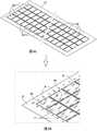
图1是包括QFN封装的封装半导体装置10的背部侧(例如,底部侧)的平面图示例。具体地,半导体装置10可以包括用于功率转换的系统级封装(SiP),该系统级封装包括半桥栅极驱动器电路和以半桥配置布置的高压增强型GaN晶体管。FIG. 1 is an example of a plan view of a backside (eg, bottom side) of a packaged
如图1所例示的,半导体装置10可以包括方形QFN封装,例如,具有9x9mm的尺寸。半导体装置10可以包括引线框,该引线框包括裸片焊盘P1、P2、P3的集合和扁平引线L、L’的集合,扁平引线L、L’被包封在模制塑料MC中并暴露在封装半导体装置10的背部侧(例如,底部侧)。As illustrated in FIG. 1 , the
仅以示例的方式,裸片焊盘P1可以电耦合到半导体装置10的接地端子或参考电压端子,裸片焊盘P2可以电耦合到半桥的低侧晶体管的源极端子或发射极端子(例如,半桥感测端子),并且裸片焊盘P3可以电耦合到半桥的高侧晶体管的源极端子或发射极端子(即,半桥布置的提供半导体装置10的输出电压的中间节点)。By way of example only, die pad P1 may be electrically coupled to a ground terminal or reference voltage terminal of
仅以示例的方式,扁平引线L可以提供半导体装置10的一个或多个输入端子和/或输出端子(例如,包括模拟和数字的输入端子和/或输出端子两者,诸如用于自举电源电压的端子、逻辑电源电压、高侧驱动器逻辑输入、低侧驱动器逻辑输入等)。仍然以非限制性示例的方式,扁平引线L’可以提供被施加到半桥的高侧晶体管的漏极或集电极的高压电源。By way of example only, the flat leads L may provide one or more input terminals and/or output terminals of the semiconductor device 10 (eg, including both analog and digital input terminals and/or output terminals, such as for a bootstrap power supply). voltage terminals, logic supply voltage, high-side driver logic input, low-side driver logic input, etc.). Still by way of non-limiting example, the flat lead L' may provide a high voltage power supply that is applied to the drain or collector of the high side transistors of the half bridge.
半导体装置10可以作为高压功率转换器操作,也就是说,可以将数百伏(例如,650V)的电压施加到与半桥的高侧晶体管的漏极或集电极耦合的引线L’。因此,如图1所示,裸片焊盘P1和裸片焊盘P3之间的爬电距离D1、裸片焊盘P2和裸片焊盘P3之间的爬电距离D2、以及裸片焊盘P3和引线L’之间的爬电距离D3可能受制于某些设计要求,例如,等于或大于2.1mm。The
应注意的是,裸片焊盘P1、P2、P3可以电耦合(例如,借助于布置在模制塑料MC内部的键合线)到引线L中的某些引线,使得即使没有通过裸片焊盘P1、P2、P3的导电性也可以实现半导体装置10到印刷电路板的电连接。It should be noted that the die pads P1, P2, P3 may be electrically coupled (eg, by means of bond wires arranged inside the molded plastic MC) to some of the leads L, so that even without die bonding The electrical conductivity of the pads P1, P2, P3 also enables the electrical connection of the
因此,本说明书的一个或多个实施例可以提供一种封装在扁平无引线封装中的半导体装置,其中裸片焊盘与被包封在模制塑料中的半导体裸片或芯片电绝缘。作为结果,裸片焊盘可以不受制于关于遵守爬电距离和/或间隙距离的设计约束。Accordingly, one or more embodiments of the present specification may provide a semiconductor device packaged in a flat no-lead package in which the die pad is electrically isolated from the semiconductor die or chip encapsulated in the molded plastic. As a result, the die pad may not be subject to design constraints regarding compliance with creepage and/or clearance distances.
例如,图2是可以应用一个或多个实施例的功率转换电路20的某些组件的简化电路框图示例。For example, FIG. 2 is a simplified circuit block diagram example of certain components of
如图2中所例示的,功率转换电路20可以包括半桥布置,该半桥布置包括高侧晶体管HST和低侧晶体管LST,例如绝缘栅双极晶体管(IGBT)。高侧晶体管HST具有耦合在高压电源节点200a(例如,被配置为接收高压正电源VPOS的节点)和输出节点200b(例如,被配置为提供半桥输出电压VOUT的节点)之间的电流路径。低侧晶体管LST具有耦合在输出节点200b和半桥感测节点200c(例如,被配置为接收高电压负电源或参考电源VNEG的节点)之间的电流路径。As illustrated in FIG. 2 , the
如图2中所例示的,功率转换电路20可以包括与高侧晶体管HST并联耦合的高侧二极管HSD、以及与低侧晶体管LST并联耦合的低侧二极管LSD。例如,高侧二极管HSD可以具有耦合到高侧晶体管HST的发射极端子或源极端子(例如,在输出节点200b处)的阳极端子、以及耦合到高侧晶体管HST的集电极端子或漏极端子(例如,在高压电源节点200a处)的阴极端子,并且低侧二极管LSD可以具有耦合到低侧晶体管LST的发射极端子或源极端子(例如,在半桥感测节点200c处)的阳极端子、以及耦合到低侧晶体管LST的集电极端子或漏极端子(例如,在输出节点200b处)的阴极端子。As illustrated in FIG. 2, the
如图2中所例示的,功率转换电路20可以包括:高侧驱动器电路202a,高侧驱动器电路202a被配置为在一个或多个输入节点204a处接收一个或多个高侧输入控制信号HSin并对应地驱动高侧晶体管HST的(栅极)控制端子;以及低侧驱动电路202b,低侧驱动电路202b被配置为在一个或多个输入节点204b处接收一个或多个低侧输入控制信号LSin并对应地驱动低侧晶体管LST的(栅极)控制端子。As illustrated in FIG. 2, the
在一个或多个实施例中,晶体管HSD、LSD、二极管HSD、LSD和驱动器电路202a、202b可以在(物理地)分开或不同的半导体芯片或裸片中实现,并且可以集成在如图3中例示的多芯片半导体装置中,图3是图示根据一个或多个实施例的半导体装置30(例如,功率转换电路20)的各种组件的图。In one or more embodiments, the transistors HSD, LSD, diode HSD, LSD and
仅以示例的方式,图3所示的半导体装置30可以集成在尺寸为17×20mm的矩形扁平无引线封装中。半导体装置30可以包括在稳态中在1200V的电压和40A的电流处操作的功率转换电路20。By way of example only, the
在一个或多个实施例中,多芯片半导体装置30的芯片或裸片(例如,HST、LST、HSD、LSD、202a、202b)可以被提供在电绝缘基板300上。In one or more embodiments, chips or dies (eg, HST, LST, HSD, LSD, 202a , 202b ) of
如图3中所例示的,承载多个裸片的单个电绝缘基板300可以被提供在半导体装置30中。As illustrated in FIG. 3 , a single
备选地,多个电绝缘基板可以被提供在半导体装置30中,例如,多至针对半导体装置30中的每个裸片提供相应的电绝缘基板。Alternatively, multiple electrically insulating substrates may be provided in
在一个或多个实施例中,(多个)电绝缘基板可以包括陶瓷基板。陶瓷材料可以包括例如氧化物和/或氮化物材料,诸如氧化铝(Al2O3)和/或氮化硅(Si3N4)。In one or more embodiments, the electrically insulating substrate(s) may comprise a ceramic substrate. Ceramic materials may include, for example, oxide and/or nitride materials, such as aluminum oxide (Al2 O3 ) and/or silicon nitride (Si3 N4 ).
在一个或多个实施例中,(多个)绝缘基板的厚度可以在100μm至1.27mm的范围内,例如约0.25mm。In one or more embodiments, the thickness of the insulating substrate(s) may be in the range of 100 μm to 1.27 mm, eg, about 0.25 mm.
在一个或多个实施例中,扁平无引线封装的引线框的(多个)常规金属裸片焊盘可以由(多个)电绝缘基板300代替,即金属引线框可以仅包括引线(例如,200a、200b、200c、204a、204b)。In one or more embodiments, the conventional metal die pad(s) of the leadframe of the flat no-lead package may be replaced by the electrically insulating substrate(s) 300 , ie the metal leadframe may include only leads (eg, 200a, 200b, 200c, 204a, 204b).
备选地,扁平无引线封装的引线框可以包括至少一个金属裸片焊盘,并且(多个)电绝缘基板300可以附接在至少一金属裸片焊盘上。例如,至少一个金属裸片焊盘可以包括单个金属裸片焊盘(例如,中央裸片焊盘)或多个金属裸片焊盘,多至针对半导体装置30中的每个裸片的相应金属裸片焊盘,其中金属裸片焊盘中的每个金属裸片焊盘具有附接在其上的相应的电绝缘基板。Alternatively, the leadframe of the flat no-lead package may include at least one metal die pad, and the electrically insulating substrate(s) 300 may be attached to the at least one metal die pad. For example, the at least one metal die pad may include a single metal die pad (eg, a central die pad) or multiple metal die pads, up to a corresponding metal for each die in
在图3中例示的一个或多个实施例中,(多个)电绝缘基板300可以具有被提供在其第一表面(例如,半导体裸片被布置在其上的上表面或顶表面)上的导电材料(例如,铜)的图案化层。这样的导电材料的图案化层可以包括(单独的)裸片附接区域和导电迹线,裸片附接区域被配置为承载半导体裸片(例如,HST、LST、HSD、LSD、202a、202b),导电迹线被配置为在不同半导体裸片之间和/或在半导体裸片与引线框的引线之间路由电信号(例如,以实现电连接)。In one or more embodiments illustrated in FIG. 3 , the electrically insulating substrate(s) 300 may have a first surface (eg, the upper or top surface on which the semiconductor die is disposed) provided on the first surface thereof. A patterned layer of conductive material (eg, copper). Such a patterned layer of conductive material may include a (separate) die attach area configured to carry a semiconductor die (eg, HST, LST, HSD, LSD, 202a, 202b) and conductive traces ), the conductive traces are configured to route electrical signals (eg, to make electrical connections) between the different semiconductor dies and/or between the semiconductor dies and the leads of the leadframe.
例如,在一个或多个实施例中,在高侧晶体管HST和高侧二极管HSD下方延伸的连续金属区域302a可以在电绝缘基板300上图案化,从而提供用于将高侧晶体管HST的漏极或集电极电耦合到高侧二极管HSD的阴极而无需使用键合线的手段。此外,连续金属区域302a可以借助于键合线304a电耦合到引线200a以接收高压正电源VPOS。For example, in one or more embodiments, a
类似地,在一个或多个实施例中,在低侧晶体管LST和低侧二极管LSD下方延伸的连续金属区域302b可以在电绝缘基板300上图案化,从而提供用于将低侧晶体管LST的漏极或集电极电耦合到低侧二极管LSD的阴极而无需使用键合线的手段。此外,连续金属区302b可以借助于键合线304b电耦合至引线200b以提供半桥输出电压VOUT。Similarly, in one or more embodiments, a
在一个或多个实施例中,被提供在(多个)电绝缘基板300的第一表面(例如,上表面或顶表面)上的导电材料的图案化层可以包括用于路由一个或多个信号的一个或多个迹线。In one or more embodiments, the patterned layer of conductive material provided on the first surface (eg, the upper surface or the top surface) of the electrically insulating substrate(s) 300 may include routing one or more One or more traces of a signal.
例如,如图3所示,迹线306a的集合可以被配置为在输入引线和/或输出引线204a与高侧驱动器电路202a之间路由信号。特别地,迹线306a中的每个迹线可以包括(例如,经由键合线)键合到相应引线204a的第一端、以及(例如,经由键合线)键合到被提供在高侧驱动器电路202a上的相应键合焊盘的第二端。For example, as shown in FIG. 3, the set of
类似地,如图3所示,迹线306b的集合可以被配置为在输入引线和/或输出引线204b与低侧驱动器电路202b之间路由信号。特别地,迹线306b中的每个迹线可以包括(例如,经由键合线)键合到相应引线204b的第一端、以及(例如,经由键合线)键合到被提供在低侧驱动器电路202b上的相应键合焊盘的第二端。Similarly, as shown in FIG. 3, the set of
因此,一个或多个实施例可以促进在半导体装置的输入焊盘和/或输出焊盘与被包封在其中的半导体裸片之间提供电连接,只要引线和半导体裸片之间的直接线键合可以通过经由(多个)电绝缘基板300上的图案化迹线的布线来代替,这可以提供增加的设计灵活性和减少的寄生电感。Accordingly, one or more embodiments may facilitate providing electrical connections between input pads and/or output pads of a semiconductor device and a semiconductor die encapsulated therein, so long as there is a direct wire between the leads and the semiconductor die Bonding may be replaced by routing through patterned trace(s) on the electrically insulating
在一个或多个实施例中,(多个)电绝缘基板300可以具有被提供在(多个)电绝缘基板300的与第一表面相对的第二表面(例如,下表面或底表面)上的导电材料层(例如,铜层)。例如,被提供在第二表面处的导电材料层可以包括单个(大)焊盘或多个焊盘,焊盘被配置用于将封装半导体装置焊接到印刷电路板上。在一个或多个实施例中,这种导电材料层的厚度可以在10μm到500μm的范围内。In one or more embodiments, the electrically insulating substrate(s) 300 may have a second surface (eg, lower surface or bottom surface) provided on the electrically insulating substrate(s) 300 opposite the first surface layer of conductive material (eg, copper). For example, the layer of conductive material provided at the second surface may comprise a single (large) pad or a plurality of pads configured for soldering the packaged semiconductor device to a printed circuit board. In one or more embodiments, the thickness of such a layer of conductive material may range from 10 μm to 500 μm.
在一个或多个实施例中,导电材料的(多个)图案化层可以通过借助于诸如直接键合铜(DBC)或直接镀铜(DPC)的技术被提供在(多个)电绝缘基板300的第一表面(例如,上表面)和/或第二表面(例如,下表面)上。In one or more embodiments, patterned layer(s) of conductive material may be provided on the electrically insulating substrate(s) by means of techniques such as direct bond copper (DBC) or direct copper plating (DPC). 300 on a first surface (eg, upper surface) and/or a second surface (eg, lower surface).
因此,一个或多个实施例可以在扁平无引线(例如,QFN)封装中提供绝缘基板,以在半导体裸片和外部裸片焊盘之间提供电绝缘。绝缘基板可以完全嵌入模制塑料中,并且封装件可以包封各种高压裸片和驱动器。(多个)暴露的焊盘因此可以是电绝缘的,使得爬电/间隙规则可以仅适用于高压引脚,例如,提供到高压电源(例如,用于电动汽车中的高压电池)的连接的引脚200a、200c。Accordingly, one or more embodiments may provide an insulating substrate in a flat no-lead (eg, QFN) package to provide electrical isolation between the semiconductor die and the external die pads. The insulating substrate can be fully embedded in the molded plastic, and the package can encapsulate a variety of high-voltage dies and drivers. The exposed pad(s) may thus be electrically isolated, so that creepage/clearance rules may only apply to high voltage pins, eg, those providing connections to high voltage power sources (eg, for high voltage batteries in electric vehicles)
应当理解,对图2和图3中所示的特定多芯片布置的参考纯粹是作为非限制性示例,并且本发明可以应用于任何类型的多芯片半导体装置,其中暴露的裸片焊盘的电绝缘可以是有益的。It should be understood that references to the specific multi-chip arrangements shown in FIGS. 2 and 3 are purely by way of non-limiting example and that the present invention may be applied to any type of multi-chip semiconductor device in which the electrical power of the exposed die pads is Insulation can be beneficial.
类似地,应当理解,在一个或多个实施例中,并非所有暴露的裸片焊盘都可以是电绝缘的。例如,一个或多个实施例可以包括电绝缘的暴露裸片焊盘和导电的暴露裸片焊盘两者。例如,可以通过借助于常规的QFN引线框布置来提供导电的暴露裸片焊盘。Similarly, it should be understood that not all exposed die pads may be electrically isolated in one or more embodiments. For example, one or more embodiments may include both electrically insulating exposed die pads and conductive exposed die pads. For example, conductive exposed die pads may be provided by means of conventional QFN leadframe arrangements.
一个或多个实施例可以涉及一种或多种制造如本文中所公开的半导体装置的方法。One or more embodiments may relate to one or more methods of fabricating a semiconductor device as disclosed herein.
例如,图4A至图4E是根据一个或多个实施例的方法的可能制造步骤的示例。For example, FIGS. 4A-4E are examples of possible fabrication steps of a method in accordance with one or more embodiments.
如图4A所示,该方法的一个步骤可以包括提供引线框LF。引线框LF可以包括多个半导体装置位置40。半导体装置位置40中的每个半导体装置位置可以被引线框的引线的相应集合包围,例如,在扁平无引线半导体装置的制造中,这样的引线按常规被布置在正方形或矩形区域的四个边上。与用于制造扁平无引线半导体装置的常规引线框相比,图4A中例示的引线框LF在半导体装置位置40处可以不包括金属裸片焊盘。As shown in Figure 4A, one step of the method may include providing a lead frame LF. The lead frame LF may include a plurality of
根据封装尺寸和条带外形尺寸,引线框LF可以被设计为包括行和列的阵列。The leadframe LF can be designed to include an array of rows and columns depending on the package size and strip outline size.
如图4B中所例示的,该方法的另一步骤可以包括提供(例如,附接)粘合在引线框LF的第一侧(例如,底部侧或后侧)的粘合带A。粘合带A可以充当临时支撑基板,该临时支撑基板促进将半导体装置放置在半导体装置位置40处,如下文所公开的。As illustrated in FIG. 4B, another step of the method may include providing (eg, attaching) adhesive tape A that adheres to the first side (eg, bottom side or back side) of the leadframe LF. Adhesive tape A may serve as a temporary support substrate that facilitates placement of the semiconductor device at
如图4C中所例示的,该方法的另一步骤可以包括提供其上具有导电层(例如,金属层)的绝缘基板S。导电层可以被图案化或成形以根据期望的图案提供导电焊盘和互连。例如,绝缘基板S可以是具有通过直接键合铜(DBC)图案化的焊盘和互连的陶瓷基板,例如“DBC母卡”。仅以示例的方式,绝缘基板S可以具有等于138x190mm的尺寸。因此,绝缘基板S可以被配置为容纳半导体裸片以提供半导体装置阵列。As illustrated in FIG. 4C, another step of the method may include providing an insulating substrate S having a conductive layer (eg, a metal layer) thereon. The conductive layers can be patterned or shaped to provide conductive pads and interconnects according to the desired pattern. For example, the insulating substrate S may be a ceramic substrate with pads and interconnects patterned by direct bonding copper (DBC), such as a "DBC mother card". Merely by way of example, the insulating substrate S may have dimensions equal to 138×190 mm. Accordingly, the insulating substrate S may be configured to accommodate semiconductor dies to provide an array of semiconductor devices.
如图4C中所例示的,该方法可以包括将半导体裸片(例如,高压组件,诸如高压晶体管、二极管和驱动器电路)(以本身已知的方式)附接在导电焊盘处。As illustrated in Figure 4C, the method may include attaching a semiconductor die (eg, high voltage components, such as high voltage transistors, diodes and driver circuits) (in a manner known per se) at conductive pads.
如图4D中所例示的,该方法的另一步骤可以包括从绝缘基板S分割半导体装置。在分割之后,可以提供多个单独的绝缘基板300,其中每个绝缘基板300具有至少一个导电裸片焊盘400和在绝缘基板300上图案化的导电迹线402,以及附接在至少一个裸片焊盘404处的至少一个半导体裸片。如图4D所示的经分割的装置42在本说明书中也可以被称为“裸半导体装置”。Another step of the method may include singulating the semiconductor device from the insulating substrate S, as illustrated in FIG. 4D . After singulation, a plurality of separate insulating
如图4E中所例示的,该方法的另一步骤可以包括在半导体装置位置40处将经分割的半导体装置42附接在粘合带A上。在这样的步骤中,粘合带A因此可以支撑引线框LF和具有附接在其上的半导体装置的绝缘基板300。As illustrated in FIG. 4E , another step of the method may include attaching the
该方法还可以包括:将半导体装置键合到在绝缘基板S上提供的导电焊盘/迹线、和/或将半导体装置到引线框LF的相应引线(例如,经由线键合),模制(例如,填充)模制塑料(例如,环氧树脂)以包封半导体装置和引线框,并且通过切割引线框来分割半导体装置以提供封装半导体装置。支撑粘合带A可以在包封步骤之后被移除。The method may further include: bonding the semiconductor device to conductive pads/traces provided on the insulating substrate S, and/or bonding the semiconductor device to the corresponding leads of the leadframe LF (eg, via wire bonding), molding Plastic (eg, epoxy) is molded (eg, filled) to encapsulate the semiconductor device and the leadframe, and the semiconductor device is singulated by cutting the leadframe to provide a packaged semiconductor device. The support adhesive tape A can be removed after the encapsulation step.
如前所述,在本说明书的一个或多个实施例中,绝缘基板300可以被提供在引线框的其他常规的金属裸片焊盘上,即,绝缘基板300可以不替换引线框的金属裸片焊盘,而是除了引线框的金属裸片焊盘之外,还可以提供绝缘基板300。As previously mentioned, in one or more embodiments of the present specification, the insulating
因此,一个或多个实施例可以涉及一种制造半导体装置的方法,该方法依赖于使用常规的扁平无引线引线框,其包括由相应引线阵列包围的金属裸片焊盘阵列。该方法与制造扁平无引线封装半导体装置的常规方法的区别在于:该方法包括在所述金属裸片焊盘处附接具有附接在其上的(多个)半导体裸片的相应绝缘基板300。Accordingly, one or more embodiments may relate to a method of fabricating a semiconductor device that relies on the use of a conventional flat leadless leadframe that includes an array of metal die pads surrounded by a corresponding array of leads. This method differs from conventional methods of manufacturing flat no-lead packaged semiconductor devices in that the method includes attaching at the metal die pads a respective insulating
因此,一个或多个实施例可以提供以下优点中的一个或多个优点:Accordingly, one or more embodiments may provide one or more of the following advantages:
通过促进裸片在封装件中的较近定位(例如,长度减少多达5倍)来减少(多个)栅极驱动器电路202a、202b与相应功率晶体管HST、LST之间的电连接的长度,从而减少(多个)寄生电感和/或连接之间的串扰;reducing the length of the electrical connections between the gate driver circuit(s) 202a, 202b and the respective power transistors HST, LST by facilitating closer positioning of the die in the package (eg, up to a 5-fold reduction in length), thereby reducing parasitic inductance(s) and/or crosstalk between connections;
借助于所插入的模制塑料MC在封装件内的高侧组件和低侧组件之间提供电绝缘(例如,相比于4mm的爬电距离,具有0.5mm的绝缘距离);Provide electrical isolation between high-side components and low-side components within the package by means of the inserted molded plastic MC (eg, with an insulation distance of 0.5mm compared to a creepage distance of 4mm);
消除与半导体裸片和环境之间的热阻相关的PCB设计约束;Eliminate PCB design constraints related to thermal resistance between semiconductor die and ambient;
提供改进的热性能(例如,由于PCB中没有单独的焊盘和大量的热通孔导致的半导体裸片和环境之间的较低热阻);以及Provides improved thermal performance (eg, lower thermal resistance between the semiconductor die and ambient due to the absence of separate pads and a large number of thermal vias in the PCB); and
避免对封装件外形的修改(例如,提供保持符合Jedec标准的可能性)。Avoid modifications to the package outline (eg, to provide the possibility to maintain Jedec compliance).
如本文中所例示的,半导体装置(例如,30)可以包括:基板(例如,300),该基板具有第一表面和第二表面,第二表面与第一表面相对;至少一个半导体裸片(例如,HST、LST、HSD、LSD、202a、202b),该至少一个半导体裸片在至少一个相应的半导体裸片安装位置处被安装在基板的所述第一表面处;多个导电引线(例如,200a、200b、200c、204a、204b),多个导电引线围绕所述基板被布置;多个导电结构(例如,304a、304b、306a、306b),将至少一个半导体裸片耦合到所述多个导电引线中的被选择的引线;以及封装模制材料(例如,MC),该封装模制材料被模制到被安装在基板的所述第一表面处的至少一个半导体裸片上、多个导电引线上和多个导电结构上,使所述基板的第二表面未被所述封装模制材料覆盖(例如,暴露在所述封装模制材料的外面)。As exemplified herein, a semiconductor device (eg, 30) may include: a substrate (eg, 300) having a first surface and a second surface, the second surface being opposite the first surface; at least one semiconductor die (eg, 300). For example, HST, LST, HSD, LSD, 202a, 202b), the at least one semiconductor die is mounted at the first surface of the substrate at at least one respective semiconductor die mounting location; a plurality of conductive leads (eg, , 200a, 200b, 200c, 204a, 204b), a plurality of conductive leads are arranged around the substrate; a plurality of conductive structures (eg, 304a, 304b, 306a, 306b), coupling at least one semiconductor die to the plurality of selected ones of the conductive leads; and an encapsulation molding material (eg, MC) molded onto at least one semiconductor die, a plurality of On the conductive leads and on the plurality of conductive structures, the second surface of the substrate is not covered by the encapsulation molding material (eg, exposed to the outside of the encapsulation molding material).
如本文中所例示的,所述基板可以包括电绝缘材料层。As exemplified herein, the substrate may include a layer of electrically insulating material.
如本文中所例示的,所述多个导电结构可以包括在基板的所述第一表面上的第一导电图案(例如,图案化金属层,可选地包括铜层)。第一导电图案可以包括:在所述至少一个半导体裸片安装位置处的至少一个裸片焊盘;和/或导电线,该导电线将至少一个半导体裸片耦合到所述多个导电引线中的被选择的引线。As exemplified herein, the plurality of conductive structures may include a first conductive pattern (eg, a patterned metal layer, optionally including a copper layer) on the first surface of the substrate. The first conductive pattern may include: at least one die pad at the at least one semiconductor die mounting location; and/or conductive lines coupling the at least one semiconductor die into the plurality of conductive leads selected leads.
如本文中所例示的,装置可以包括多个半导体裸片,多个半导体裸片在相应的多个半导体裸片安装位置处被安装在基板的所述第一表面处,并且导电图案可以包括导电线,导电线将所述多个半导体裸片中的至少一个半导体裸片耦合到所述多个半导体裸片中的至少另一个半导体裸片。As exemplified herein, an apparatus may include a plurality of semiconductor dies mounted at the first surface of the substrate at respective plurality of semiconductor die mounting locations, and the conductive pattern may include conductive A wire, a conductive wire couples at least one semiconductor die of the plurality of semiconductor dies to at least another semiconductor die of the plurality of semiconductor dies.
如本文中所例示的,所述多个半导体裸片可以包括:第一晶体管裸片(例如,HST)、第二晶体管裸片(例如,LST)、第一二极管裸片(例如,HSD)、第二二极管裸片(例如,LSD)、第一晶体管驱动电路裸片(例如,202a)和第二晶体管驱动电路裸片(例如,202b)。围绕所述基板布置的多个导电引线可以包括:控制信号引线(例如,204a)的第一集合、控制信号引线(例如,204b)的第二集合、正电压供电引线(例如,200a)、负电压供电引线或参考电压供电引线(例如,200c)和输出电压引线(例如,200b)。基板的所述第一表面上的所述导电图案中的导电线可以包括:第一导电线(例如,302a),将第一晶体管裸片的漏极端子或集电极端子耦合到第一二极管的阴极端子;第二导电线(例如,302b),将第二晶体管裸片的漏极端子或集电极端子耦合到第二二极管裸片的阴极端子;导电线(例如,306a)的第一子集,被配置为从基板的外围朝向第一晶体管驱动电路裸片路由信号;以及导电线(例如,306b)的第二子集,被配置为从基板的外围朝向第二晶体管驱动电路裸片路由信号。多个导电结构还可以包括键合线,键合线将所述多个导电引线中的被选择的引线耦合到所述导电线。As exemplified herein, the plurality of semiconductor dies may include: a first transistor die (eg, HST), a second transistor die (eg, LST), a first diode die (eg, HSD) ), a second diode die (eg, LSD), a first transistor driver circuit die (eg, 202a), and a second transistor driver circuit die (eg, 202b). The plurality of conductive leads arranged around the substrate may include: a first set of control signal leads (eg, 204a), a second set of control signal leads (eg, 204b), positive voltage supply leads (eg, 200a), negative A voltage supply lead or reference voltage supply lead (eg, 200c) and an output voltage lead (eg, 200b). The conductive lines in the conductive pattern on the first surface of the substrate may include a first conductive line (eg, 302a) coupling a drain terminal or collector terminal of a first transistor die to a first diode the cathode terminal of the tube; a second conductive line (eg, 302b) coupling the drain terminal or collector terminal of the second transistor die to the cathode terminal of the second diode die; the conductive line (eg, 306a) a first subset configured to route signals from the periphery of the substrate toward the first transistor driver circuit die; and a second subset of conductive lines (eg, 306b) configured to route signals from the periphery of the substrate toward the second transistor driver circuit The die routes the signals. The plurality of conductive structures may also include bond wires that couple selected ones of the plurality of conductive leads to the conductive wires.
如本文中所例示的,所述电绝缘材料层可以包括陶瓷材料,可选地氧化物材料和/或氮化物材料,可选地氧化铝和/或氮化硅。As exemplified herein, the layer of electrically insulating material may comprise a ceramic material, optionally an oxide material and/or a nitride material, optionally an aluminum oxide and/or a silicon nitride.
如本文中所例示的,所述电绝缘材料层的厚度可以在100μm至1.27mm的范围内,可选地等于0.25mm。As exemplified herein, the thickness of the layer of electrically insulating material may be in the range of 100 μm to 1.27 mm, optionally equal to 0.25 mm.
如本文中所例示的,所述基板可以包括导电材料层(例如,金属材料层,可选地铜层),导电材料层被暴露于所述封装模制材料的外表面(例如,被配置为提供用于将半导体装置焊接到印刷电路板的焊接焊盘)。As exemplified herein, the substrate may include a layer of conductive material (eg, a layer of metallic material, optionally a layer of copper) exposed to an outer surface of the encapsulation molding material (eg, configured to be Provides solder pads for soldering semiconductor devices to printed circuit boards).
如本文中所例示的,被暴露于所述封装模制材料的外表面的所述导电材料层可以包括:在基板的所述第二表面上的第二导电图案(例如,金属层,可选地包括铜层)。以示例的方式,第二导电图案的厚度可以在几微米(例如,10μm)至厚铜(例如,500μm)的范围内。As exemplified herein, the layer of conductive material exposed to the outer surface of the encapsulation molding material may include: a second conductive pattern (eg, a metal layer, optional) on the second surface of the substrate ground including copper layers). By way of example, the thickness of the second conductive pattern may range from a few microns (eg, 10 μm) to thick copper (eg, 500 μm).
如本文中所例示的,暴露于所述封装模制材料的外表面的所述导电材料层可以包括:被提供在装置中的引线框的裸片焊盘。As exemplified herein, the layer of conductive material exposed to the outer surface of the encapsulation molding material may include a die pad of a lead frame provided in a device.
如本文中所例示的,装置可以包括扁平无引线封装,可选地方形扁平无引线封装。As exemplified herein, the device may comprise a flat no-lead package, optionally a shape flat no-lead package.
如本文中所例示的,所述至少一个半导体裸片可以包括:至少一个高压半导体裸片,并且所述基板可以包括电绝缘材料层,电绝缘材料层被配置为提供所述至少一个高压半导体裸片的高压绝缘。As exemplified herein, the at least one semiconductor die may include at least one high voltage semiconductor die, and the substrate may include a layer of electrically insulating material configured to provide the at least one high voltage semiconductor die high-voltage insulation of the sheet.
如本文中所例示的,制造封装半导体装置的方法可以包括:提供至少一个裸半导体装置(例如,42),其中至少一个裸半导体装置包括:基板,该基板包括电绝缘材料层,该基板具有第一表面和第二表面,第二表面与第一表面相对;导电结构,导电结构被形成在基板的所述第一表面处;以及至少一个半导体裸片,至少一个半导体裸片被安装在基板的所述第一表面处;提供引线框(例如,LF),引线框包括围绕至少一个相应半导体装置位置(例如,40)布置的至少一个导电引线集合;将所述至少一个裸半导体装置定位在所述引线框内的所述至少一个相应半导体装置位置处;将所述至少一个半导体裸片电耦合(例如,线键合)到所述导电结构和/或所述至少一个相应导电引线集合;以及将封装模制材料模制到所述至少一个裸半导体装置上,使所述基板的所述第二表面未被所述封装模制材料覆盖(例如,暴露在所述封装模制材料的外面)。As exemplified herein, a method of fabricating a packaged semiconductor device may include providing at least one bare semiconductor device (eg, 42 ), wherein the at least one bare semiconductor device includes a substrate including a layer of electrically insulating material, the substrate having a first a surface and a second surface opposite the first surface; a conductive structure formed at the first surface of the substrate; and at least one semiconductor die mounted on the substrate at the first surface; providing a lead frame (eg, LF) including at least one set of conductive leads arranged around at least one respective semiconductor device location (eg, 40 ); positioning the at least one bare semiconductor device at the at the at least one respective semiconductor device location within the lead frame; electrically coupling (eg, wire bonding) the at least one semiconductor die to the conductive structure and/or the at least one respective set of conductive leads; and molding encapsulation molding material onto the at least one bare semiconductor device such that the second surface of the substrate is uncovered (eg, exposed on the outside of the encapsulation molding material) .
如本文中所例示的,将所述至少一个裸半导体装置定位在所述至少一个相应半导体装置位置处可以包括:在所述引线框的一侧附接粘合带(例如,A),并且在所述引线框内的所述至少一个相应半导体装置位置处,将所述至少一个裸半导体装置附接到所述粘合带上。As exemplified herein, positioning the at least one bare semiconductor device at the at least one respective semiconductor device location may include attaching an adhesive tape (eg, A) on one side of the leadframe, and The at least one bare semiconductor device is attached to the adhesive tape at the at least one respective semiconductor device location within the lead frame.
如本文中所例示的,所述引线框可以包括至少一个裸片焊盘,至少一个裸片焊盘被布置在所述至少一个相应半导体装置位置处,并且将所述至少一个裸半导体装置定位在所述至少一个相应半导体装置位置处可以包括:将所述至少一个裸半导体装置安装在引线框的所述至少一个裸片焊盘上。As exemplified herein, the leadframe may include at least one die pad disposed at the at least one respective semiconductor device location and positioning the at least one bare semiconductor device at The at least one respective semiconductor device location may include mounting the at least one bare semiconductor device on the at least one die pad of the leadframe.
在不损害基本原理的情况下,可以相对于已经仅以示例的方式描述的内容变化细节和实施例,甚至显著地变化细节和实施例,而不脱离保护范围。Without prejudice to the underlying principles, details and embodiments may vary, even significantly, from what has been described by way of example only, without departing from the scope of protection.
权利要求是本文中提供的关于实施例的技术教导的组成部分。保护范围由所附权利要求确定。The claims are an integral part of the technical teaching provided herein with respect to the embodiments. The scope of protection is determined by the appended claims.
Claims (17)
Translated fromChineseApplications Claiming Priority (4)
| Application Number | Priority Date | Filing Date | Title |
|---|---|---|---|
| IT102020000023122 | 2020-09-30 | ||
| IT202000023122 | 2020-09-30 | ||
| US17/487,772 | 2021-09-28 | ||
| US17/487,772US12040263B2 (en) | 2020-09-30 | 2021-09-28 | Semiconductor device with die mounted to an insulating substrate and corresponding method of manufacturing semiconductor devices |
Publications (2)
| Publication Number | Publication Date |
|---|---|
| CN114334933Atrue CN114334933A (en) | 2022-04-12 |
| CN114334933B CN114334933B (en) | 2025-09-09 |
Family
ID=73643296
Family Applications (2)
| Application Number | Title | Priority Date | Filing Date |
|---|---|---|---|
| CN202122404911.9UActiveCN216871961U (en) | 2020-09-30 | 2021-09-29 | semiconductor device |
| CN202111150863.3AActiveCN114334933B (en) | 2020-09-30 | 2021-09-29 | Semiconductor device and corresponding method of manufacturing semiconductor device |
Family Applications Before (1)
| Application Number | Title | Priority Date | Filing Date |
|---|---|---|---|
| CN202122404911.9UActiveCN216871961U (en) | 2020-09-30 | 2021-09-29 | semiconductor device |
Country Status (2)
| Country | Link |
|---|---|
| US (2) | US12040263B2 (en) |
| CN (2) | CN216871961U (en) |
Families Citing this family (5)
| Publication number | Priority date | Publication date | Assignee | Title |
|---|---|---|---|---|
| US12040263B2 (en)* | 2020-09-30 | 2024-07-16 | Stmicroelectronics S.R.L. | Semiconductor device with die mounted to an insulating substrate and corresponding method of manufacturing semiconductor devices |
| CN115443533A (en)* | 2020-11-25 | 2022-12-06 | 富士电机株式会社 | semiconductor module |
| US20250316657A1 (en)* | 2022-10-12 | 2025-10-09 | Mitsubishi Electric Corporation | Semiconductor device |
| DE102023200837A1 (en)* | 2023-02-02 | 2024-08-08 | Carl Zeiss Ag | Sample vessel for the cultivation of biological samples, device for its operation and microscope |
| JP2025115679A (en)* | 2024-01-26 | 2025-08-07 | ミネベアパワーデバイス株式会社 | Semiconductor device and power conversion device using the same |
Citations (16)
| Publication number | Priority date | Publication date | Assignee | Title |
|---|---|---|---|---|
| US5365409A (en)* | 1993-02-20 | 1994-11-15 | Vlsi Technology, Inc. | Integrated circuit package design having an intermediate die-attach substrate bonded to a leadframe |
| US5386141A (en)* | 1992-03-31 | 1995-01-31 | Vlsi Technology, Inc. | Leadframe having one or more power/ground planes without vias |
| US6879034B1 (en)* | 2003-05-01 | 2005-04-12 | Amkor Technology, Inc. | Semiconductor package including low temperature co-fired ceramic substrate |
| US20070196950A1 (en)* | 2006-02-21 | 2007-08-23 | Nobuyuki Shirai | Semiconductor device and manufacturing the same |
| US20100178550A1 (en)* | 2009-01-13 | 2010-07-15 | Magistor Technologies, LLC | Magistor technology |
| WO2010083753A1 (en)* | 2009-01-21 | 2010-07-29 | 成都芯源系统有限公司 | Circuit and method for providing power supply voltage for wireless network card |
| US20110037170A1 (en)* | 2009-08-12 | 2011-02-17 | Renesas Electronics Corporation | Electronic device and manufacturing method therefor |
| US8076184B1 (en)* | 2010-08-16 | 2011-12-13 | Stats Chippac, Ltd. | Semiconductor device and method of forming wafer-level multi-row etched leadframe with base leads and embedded semiconductor die |
| US20120164794A1 (en)* | 2010-12-28 | 2012-06-28 | Yan Xun Xue | Method of making a copper wire bond package |
| CN103579015A (en)* | 2012-07-18 | 2014-02-12 | 嘉盛马来西亚公司 | Semiconductor package and method for forming the same |
| CN104348339A (en)* | 2013-08-01 | 2015-02-11 | 英飞凌科技奥地利有限公司 | Switch circuit arrangements and method for powering a driver circuit |
| WO2016085124A1 (en)* | 2014-11-28 | 2016-06-02 | 류태하 | Flicker-free ac led lighting system |
| US20180218969A1 (en)* | 2017-01-27 | 2018-08-02 | Renesas Electronics Corporation | Semiconductor device |
| CN109524390A (en)* | 2017-09-20 | 2019-03-26 | 瑞萨电子株式会社 | Semiconductor device |
| CN216871961U (en)* | 2020-09-30 | 2022-07-01 | 意法半导体股份有限公司 | semiconductor device |
| US20230197543A1 (en)* | 2021-12-21 | 2023-06-22 | Intel Corporation | Microelectronic assemblies with adaptive multi-layer encapsulation materials |
Family Cites Families (14)
| Publication number | Priority date | Publication date | Assignee | Title |
|---|---|---|---|---|
| US7342318B2 (en)* | 2003-01-21 | 2008-03-11 | Siliconware Precision Industries Co., Ltd. | Semiconductor package free of substrate and fabrication method thereof |
| US8048358B2 (en)* | 2006-04-18 | 2011-11-01 | Texas Instruments Incorporated | Pop semiconductor device manufacturing method |
| TWI389283B (en) | 2007-10-22 | 2013-03-11 | Analog Devices Inc | Packaged microchip with spacer for mitigating electrical leakage between components |
| KR101524545B1 (en)* | 2008-02-28 | 2015-06-01 | 페어차일드코리아반도체 주식회사 | Power device package and the method of fabricating the same |
| US8273602B2 (en)* | 2008-03-11 | 2012-09-25 | Stats Chippac Ltd. | Integrated circuit package system with integration port |
| TW201011869A (en)* | 2008-09-10 | 2010-03-16 | Cyntec Co Ltd | Chip package structure |
| JP5164780B2 (en) | 2008-10-14 | 2013-03-21 | 日立オートモティブシステムズ株式会社 | Shift control device and electronic circuit sealing device |
| KR101321282B1 (en)* | 2011-06-17 | 2013-10-28 | 삼성전기주식회사 | Power module package and system module having the same |
| US20130015569A1 (en)* | 2011-07-12 | 2013-01-17 | Great Wall Semiconductor Corporation | Semiconductor Device and Method of Forming Substrate With Seated Plane for Mating With Bumped Semiconductor Die |
| EP2790213A3 (en) | 2013-04-11 | 2015-04-01 | Chun Ho Fan | Cavity package |
| DE102013104081B3 (en) | 2013-04-23 | 2014-05-15 | Semikron Elektronik Gmbh & Co. Kg | 3-level power converter half-bridge |
| US10074590B1 (en) | 2017-07-02 | 2018-09-11 | Infineon Technologies Ag | Molded package with chip carrier comprising brazed electrically conductive layers |
| JP7071499B2 (en) | 2018-06-20 | 2022-05-19 | ローム株式会社 | Semiconductor device |
| EP3633715A1 (en)* | 2018-10-02 | 2020-04-08 | Infineon Technologies Austria AG | Multi-clip structure for die bonding |
- 2021
- 2021-09-28USUS17/487,772patent/US12040263B2/enactiveActive
- 2021-09-29CNCN202122404911.9Upatent/CN216871961U/enactiveActive
- 2021-09-29CNCN202111150863.3Apatent/CN114334933B/enactiveActive
- 2024
- 2024-07-16USUS18/774,478patent/US20240371738A1/enactivePending
Patent Citations (16)
| Publication number | Priority date | Publication date | Assignee | Title |
|---|---|---|---|---|
| US5386141A (en)* | 1992-03-31 | 1995-01-31 | Vlsi Technology, Inc. | Leadframe having one or more power/ground planes without vias |
| US5365409A (en)* | 1993-02-20 | 1994-11-15 | Vlsi Technology, Inc. | Integrated circuit package design having an intermediate die-attach substrate bonded to a leadframe |
| US6879034B1 (en)* | 2003-05-01 | 2005-04-12 | Amkor Technology, Inc. | Semiconductor package including low temperature co-fired ceramic substrate |
| US20070196950A1 (en)* | 2006-02-21 | 2007-08-23 | Nobuyuki Shirai | Semiconductor device and manufacturing the same |
| US20100178550A1 (en)* | 2009-01-13 | 2010-07-15 | Magistor Technologies, LLC | Magistor technology |
| WO2010083753A1 (en)* | 2009-01-21 | 2010-07-29 | 成都芯源系统有限公司 | Circuit and method for providing power supply voltage for wireless network card |
| US20110037170A1 (en)* | 2009-08-12 | 2011-02-17 | Renesas Electronics Corporation | Electronic device and manufacturing method therefor |
| US8076184B1 (en)* | 2010-08-16 | 2011-12-13 | Stats Chippac, Ltd. | Semiconductor device and method of forming wafer-level multi-row etched leadframe with base leads and embedded semiconductor die |
| US20120164794A1 (en)* | 2010-12-28 | 2012-06-28 | Yan Xun Xue | Method of making a copper wire bond package |
| CN103579015A (en)* | 2012-07-18 | 2014-02-12 | 嘉盛马来西亚公司 | Semiconductor package and method for forming the same |
| CN104348339A (en)* | 2013-08-01 | 2015-02-11 | 英飞凌科技奥地利有限公司 | Switch circuit arrangements and method for powering a driver circuit |
| WO2016085124A1 (en)* | 2014-11-28 | 2016-06-02 | 류태하 | Flicker-free ac led lighting system |
| US20180218969A1 (en)* | 2017-01-27 | 2018-08-02 | Renesas Electronics Corporation | Semiconductor device |
| CN109524390A (en)* | 2017-09-20 | 2019-03-26 | 瑞萨电子株式会社 | Semiconductor device |
| CN216871961U (en)* | 2020-09-30 | 2022-07-01 | 意法半导体股份有限公司 | semiconductor device |
| US20230197543A1 (en)* | 2021-12-21 | 2023-06-22 | Intel Corporation | Microelectronic assemblies with adaptive multi-layer encapsulation materials |
Also Published As
| Publication number | Publication date |
|---|---|
| US12040263B2 (en) | 2024-07-16 |
| CN114334933B (en) | 2025-09-09 |
| US20240371738A1 (en) | 2024-11-07 |
| CN216871961U (en) | 2022-07-01 |
| US20220102258A1 (en) | 2022-03-31 |
Similar Documents
| Publication | Publication Date | Title |
|---|---|---|
| CN216871961U (en) | semiconductor device | |
| US10128165B2 (en) | Package with vertically spaced partially encapsulated contact structures | |
| US8575733B2 (en) | Semiconductor device | |
| US9468087B1 (en) | Power module with improved cooling and method for making | |
| CN103839913B (en) | Semiconductor packages and methods of formation thereof | |
| US10985110B2 (en) | Semiconductor package having an electromagnetic shielding structure and method for producing the same | |
| US11222832B2 (en) | Power semiconductor device package | |
| CN217719586U (en) | electronic device | |
| US12293961B2 (en) | Method of manufacture for a cascode semiconductor device | |
| CN108155168B (en) | Electronic device | |
| CN114551372A (en) | Package having at least one step on electrically insulating carrier and encapsulating material | |
| US20250079275A1 (en) | Package with transistor chip between carrier and conductive structure and with thermally conductive electrically insulating layer | |
| US10964642B2 (en) | Semiconductor module comprising transistor chips, diode chips and driver chips arranged in a common plane | |
| US20230307424A1 (en) | Semiconductor device | |
| US12237248B2 (en) | Semiconductor device and method for manufacture of semiconductor device | |
| CN111244061B (en) | Packaging structure of gallium nitride equipment | |
| CN111554666B (en) | Power semiconductor device packages | |
| US20230245951A1 (en) | Semiconductor device | |
| US20250218914A1 (en) | Package with component-carrying intermediate structure and additional carrier having reference potential structure | |
| EP4261878A1 (en) | Multi-chip device with gate redistribution structure | |
| US20250054840A1 (en) | Power module having a lead frame that provides substrate support and forms terminals of the power module | |
| US20240395676A1 (en) | Package with Single Integral Body Carrying Two Transistor Chips with Half Bridge Configuration | |
| JP2013128040A (en) | Semiconductor device | |
| JP2002110892A (en) | Multi-chip semiconductor device |
Legal Events
| Date | Code | Title | Description |
|---|---|---|---|
| PB01 | Publication | ||
| PB01 | Publication | ||
| SE01 | Entry into force of request for substantive examination | ||
| SE01 | Entry into force of request for substantive examination | ||
| GR01 | Patent grant | ||
| GR01 | Patent grant |