CN114326318A - Information processing apparatus, inspection method, storage medium, exposure apparatus, determination method, and article manufacturing method - Google Patents
Information processing apparatus, inspection method, storage medium, exposure apparatus, determination method, and article manufacturing methodDownload PDFInfo
- Publication number
- CN114326318A CN114326318ACN202111118738.4ACN202111118738ACN114326318ACN 114326318 ACN114326318 ACN 114326318ACN 202111118738 ACN202111118738 ACN 202111118738ACN 114326318 ACN114326318 ACN 114326318A
- Authority
- CN
- China
- Prior art keywords
- substrate
- inspection
- information indicating
- learning
- development state
- Prior art date
- Legal status (The legal status is an assumption and is not a legal conclusion. Google has not performed a legal analysis and makes no representation as to the accuracy of the status listed.)
- Pending
Links
Images


Classifications
- G—PHYSICS
- G03—PHOTOGRAPHY; CINEMATOGRAPHY; ANALOGOUS TECHNIQUES USING WAVES OTHER THAN OPTICAL WAVES; ELECTROGRAPHY; HOLOGRAPHY
- G03F—PHOTOMECHANICAL PRODUCTION OF TEXTURED OR PATTERNED SURFACES, e.g. FOR PRINTING, FOR PROCESSING OF SEMICONDUCTOR DEVICES; MATERIALS THEREFOR; ORIGINALS THEREFOR; APPARATUS SPECIALLY ADAPTED THEREFOR
- G03F1/00—Originals for photomechanical production of textured or patterned surfaces, e.g., masks, photo-masks, reticles; Mask blanks or pellicles therefor; Containers specially adapted therefor; Preparation thereof
- G03F1/68—Preparation processes not covered by groups G03F1/20 - G03F1/50
- G03F1/70—Adapting basic layout or design of masks to lithographic process requirements, e.g., second iteration correction of mask patterns for imaging
- G—PHYSICS
- G06—COMPUTING OR CALCULATING; COUNTING
- G06T—IMAGE DATA PROCESSING OR GENERATION, IN GENERAL
- G06T7/00—Image analysis
- G06T7/0002—Inspection of images, e.g. flaw detection
- G06T7/0004—Industrial image inspection
- G—PHYSICS
- G03—PHOTOGRAPHY; CINEMATOGRAPHY; ANALOGOUS TECHNIQUES USING WAVES OTHER THAN OPTICAL WAVES; ELECTROGRAPHY; HOLOGRAPHY
- G03F—PHOTOMECHANICAL PRODUCTION OF TEXTURED OR PATTERNED SURFACES, e.g. FOR PRINTING, FOR PROCESSING OF SEMICONDUCTOR DEVICES; MATERIALS THEREFOR; ORIGINALS THEREFOR; APPARATUS SPECIALLY ADAPTED THEREFOR
- G03F7/00—Photomechanical, e.g. photolithographic, production of textured or patterned surfaces, e.g. printing surfaces; Materials therefor, e.g. comprising photoresists; Apparatus specially adapted therefor
- G03F7/70—Microphotolithographic exposure; Apparatus therefor
- G03F7/70483—Information management; Active and passive control; Testing; Wafer monitoring, e.g. pattern monitoring
- G03F7/70491—Information management, e.g. software; Active and passive control, e.g. details of controlling exposure processes or exposure tool monitoring processes
- G03F7/705—Modelling or simulating from physical phenomena up to complete wafer processes or whole workflow in wafer productions
- G—PHYSICS
- G03—PHOTOGRAPHY; CINEMATOGRAPHY; ANALOGOUS TECHNIQUES USING WAVES OTHER THAN OPTICAL WAVES; ELECTROGRAPHY; HOLOGRAPHY
- G03F—PHOTOMECHANICAL PRODUCTION OF TEXTURED OR PATTERNED SURFACES, e.g. FOR PRINTING, FOR PROCESSING OF SEMICONDUCTOR DEVICES; MATERIALS THEREFOR; ORIGINALS THEREFOR; APPARATUS SPECIALLY ADAPTED THEREFOR
- G03F7/00—Photomechanical, e.g. photolithographic, production of textured or patterned surfaces, e.g. printing surfaces; Materials therefor, e.g. comprising photoresists; Apparatus specially adapted therefor
- G03F7/70—Microphotolithographic exposure; Apparatus therefor
- G03F7/70483—Information management; Active and passive control; Testing; Wafer monitoring, e.g. pattern monitoring
- G03F7/70605—Workpiece metrology
- G03F7/70616—Monitoring the printed patterns
- G03F7/70625—Dimensions, e.g. line width, critical dimension [CD], profile, sidewall angle or edge roughness
- G—PHYSICS
- G03—PHOTOGRAPHY; CINEMATOGRAPHY; ANALOGOUS TECHNIQUES USING WAVES OTHER THAN OPTICAL WAVES; ELECTROGRAPHY; HOLOGRAPHY
- G03F—PHOTOMECHANICAL PRODUCTION OF TEXTURED OR PATTERNED SURFACES, e.g. FOR PRINTING, FOR PROCESSING OF SEMICONDUCTOR DEVICES; MATERIALS THEREFOR; ORIGINALS THEREFOR; APPARATUS SPECIALLY ADAPTED THEREFOR
- G03F7/00—Photomechanical, e.g. photolithographic, production of textured or patterned surfaces, e.g. printing surfaces; Materials therefor, e.g. comprising photoresists; Apparatus specially adapted therefor
- G03F7/70—Microphotolithographic exposure; Apparatus therefor
- G03F7/70483—Information management; Active and passive control; Testing; Wafer monitoring, e.g. pattern monitoring
- G03F7/70605—Workpiece metrology
- G03F7/706835—Metrology information management or control
- G03F7/706839—Modelling, e.g. modelling scattering or solving inverse problems
- G03F7/706841—Machine learning
- G—PHYSICS
- G03—PHOTOGRAPHY; CINEMATOGRAPHY; ANALOGOUS TECHNIQUES USING WAVES OTHER THAN OPTICAL WAVES; ELECTROGRAPHY; HOLOGRAPHY
- G03F—PHOTOMECHANICAL PRODUCTION OF TEXTURED OR PATTERNED SURFACES, e.g. FOR PRINTING, FOR PROCESSING OF SEMICONDUCTOR DEVICES; MATERIALS THEREFOR; ORIGINALS THEREFOR; APPARATUS SPECIALLY ADAPTED THEREFOR
- G03F7/00—Photomechanical, e.g. photolithographic, production of textured or patterned surfaces, e.g. printing surfaces; Materials therefor, e.g. comprising photoresists; Apparatus specially adapted therefor
- G03F7/70—Microphotolithographic exposure; Apparatus therefor
- G03F7/708—Construction of apparatus, e.g. environment aspects, hygiene aspects or materials
- G03F7/70908—Hygiene, e.g. preventing apparatus pollution, mitigating effect of pollution or removing pollutants from apparatus
- G03F7/70941—Stray fields and charges, e.g. stray light, scattered light, flare, transmission loss
- G—PHYSICS
- G06—COMPUTING OR CALCULATING; COUNTING
- G06T—IMAGE DATA PROCESSING OR GENERATION, IN GENERAL
- G06T2207/00—Indexing scheme for image analysis or image enhancement
- G06T2207/20—Special algorithmic details
- G06T2207/20081—Training; Learning
- G—PHYSICS
- G06—COMPUTING OR CALCULATING; COUNTING
- G06T—IMAGE DATA PROCESSING OR GENERATION, IN GENERAL
- G06T2207/00—Indexing scheme for image analysis or image enhancement
- G06T2207/20—Special algorithmic details
- G06T2207/20084—Artificial neural networks [ANN]
- G—PHYSICS
- G06—COMPUTING OR CALCULATING; COUNTING
- G06T—IMAGE DATA PROCESSING OR GENERATION, IN GENERAL
- G06T2207/00—Indexing scheme for image analysis or image enhancement
- G06T2207/30—Subject of image; Context of image processing
- G06T2207/30108—Industrial image inspection
- G06T2207/30148—Semiconductor; IC; Wafer
Landscapes
- Engineering & Computer Science (AREA)
- General Physics & Mathematics (AREA)
- Physics & Mathematics (AREA)
- Computer Vision & Pattern Recognition (AREA)
- Health & Medical Sciences (AREA)
- Quality & Reliability (AREA)
- Theoretical Computer Science (AREA)
- Epidemiology (AREA)
- Public Health (AREA)
- Environmental & Geological Engineering (AREA)
- Atmospheric Sciences (AREA)
- Life Sciences & Earth Sciences (AREA)
- Artificial Intelligence (AREA)
- Evolutionary Computation (AREA)
- Medical Informatics (AREA)
- Software Systems (AREA)
- Exposure And Positioning Against Photoresist Photosensitive Materials (AREA)
- Exposure Of Semiconductors, Excluding Electron Or Ion Beam Exposure (AREA)
Abstract
Translated fromChinese
Description
Translated fromChinese技术领域technical field
本公开涉及信息处理装置、检查方法、存储介质、曝光装置、确定方法和物品制造方法。The present disclosure relates to an information processing apparatus, an inspection method, a storage medium, an exposure apparatus, a determination method, and an article manufacturing method.
背景技术Background technique
在制造诸如半导体器件之类的物品期间的光刻工艺中,首先执行用于通过向基板施加抗蚀剂而在基板上形成抗蚀剂膜的形成工艺。接下来,执行用于利用透射通过上面形成有图案的掩模的光对形成在基板上的抗蚀剂膜进行曝光的曝光工艺。然后,执行用于显影经曝光的抗蚀剂膜的显影工艺。依次执行形成工艺、曝光工艺和显影工艺,从而在基板上形成图案。In a photolithography process during manufacture of an article such as a semiconductor device, a formation process for forming a resist film on a substrate by applying a resist to the substrate is first performed. Next, an exposure process for exposing the resist film formed on the substrate with light transmitted through the mask on which the pattern is formed is performed. Then, a development process for developing the exposed resist film is performed. A forming process, an exposing process, and a developing process are sequentially performed to form a pattern on the substrate.
为了确定曝光工艺中的曝光条件,诸如曝光量和掩模尺寸,执行用于检查在预定条件下经受形成工艺、曝光工艺和显影工艺的基板的显影状态的检查工艺。曝光工艺中的曝光条件基于检查工艺中获得的基板的显影状态的检查结果来确定。In order to determine the exposure conditions in the exposure process, such as the exposure amount and the mask size, an inspection process for inspecting the development state of the substrate subjected to the formation process, the exposure process, and the development process under predetermined conditions is performed. The exposure conditions in the exposure process are determined based on the inspection result of the developed state of the substrate obtained in the inspection process.
日本专利申请公开No.2000-164485讨论了一种抗蚀剂图案检查方法,该方法能够在光刻工艺中容易地识别可能发生图案缺陷的部分以及适当的曝光量。在这种检查方法中,在以一定量的增量增加曝光量的同时,以图案曝光上面有和没有背景图案的基板(晶片),从而创建用于检查的基板。然后,将上面没有背景图案的基板的图案形状与上面有背景图案的基板的图案形状彼此进行比较,从而识别发生图案形状缺陷的部分以及发生图案形状缺陷时的曝光量。Japanese Patent Application Laid-Open No. 2000-164485 discusses a resist pattern inspection method capable of easily identifying portions where pattern defects may occur and an appropriate exposure amount in a photolithography process. In this inspection method, a substrate (wafer) with and without a background pattern on it is pattern exposed while increasing the exposure by a certain amount of increments, thereby creating a substrate for inspection. Then, the pattern shape of the substrate without the background pattern thereon and the pattern shape of the substrate with the background pattern thereon are compared with each other to identify the portion where the pattern shape defect occurs and the exposure amount when the pattern shape defect occurs.
在根据日本专利申请公开No.2000-164485的检查方法中,为了识别发生缺陷时的曝光量,将形成在基板上的相同形状的图案彼此进行比较,并将图案不彼此匹配的部分确定为缺陷。In the inspection method according to Japanese Patent Application Laid-Open No. 2000-164485, in order to identify the exposure amount when a defect occurs, patterns of the same shape formed on a substrate are compared with each other, and portions where the patterns do not match each other are determined as defects .
但是,在根据日本专利申请公开No.2000-164485的检查方法中,图案形状的影响反映在确定结果中。因此,难以执行限于曝光装置的光学性能方面的检查。为了解决这个问题,在基板的显影状态的检查中,在没有上面形成有图案的掩模的情况下曝光基板,将经曝光的基板显影,并且检查基板的显影状态。在这种检查中,经显影的基板上没有形成图案。However, in the inspection method according to Japanese Patent Application Laid-Open No. 2000-164485, the influence of the pattern shape is reflected in the determination result. Therefore, it is difficult to perform inspection limited to the optical performance of the exposure apparatus. In order to solve this problem, in the inspection of the development state of the substrate, the substrate is exposed without a mask on which a pattern is formed, the exposed substrate is developed, and the development state of the substrate is inspected. In this inspection, no pattern was formed on the developed substrate.
发明内容SUMMARY OF THE INVENTION
本公开针对提供一种能够在不进行图案形状比较的情况下检查基板的显影状态的信息处理装置。本公开还针对检查方法、存储介质、曝光装置、确定方法和物品制造方法。The present disclosure is directed to providing an information processing apparatus capable of inspecting the development state of a substrate without performing pattern shape comparison. The present disclosure is also directed to inspection methods, storage media, exposure apparatuses, determination methods, and article manufacturing methods.
根据本公开的一个方面,一种被配置为检查基板的显影状态的信息处理装置包括检查单元,该检查单元被配置为将显影的第二基板的捕获图像输入到学习模型以获取检查数据,该检查数据包括指示第二基板的第二显影状态的信息,学习模型是通过使用学习数据进行学习而获得的,学习数据包括显影的第一基板的捕获图像和指示第一基板的第一显影状态的信息。According to an aspect of the present disclosure, an information processing apparatus configured to inspect a development state of a substrate includes an inspection unit configured to input a captured image of a developed second substrate to a learning model to acquire inspection data, the inspection unit being The inspection data includes information indicating the second development state of the second substrate, and the learning model is obtained by performing learning using the learning data including the captured image of the developed first substrate and the information indicating the first development state of the first substrate. information.
通过参考附图对示例性实施例的以下描述,本公开的其他特征将变得清楚。Other features of the present disclosure will become apparent from the following description of exemplary embodiments with reference to the accompanying drawings.
附图说明Description of drawings
图1是例示曝光装置和涂覆/显影装置的配置的图。FIG. 1 is a diagram illustrating the configuration of an exposure apparatus and a coating/developing apparatus.
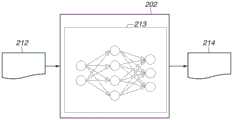
图2是例示曝光装置的图。FIG. 2 is a diagram illustrating an exposure apparatus.
图3是例示信息处理装置的配置的图。FIG. 3 is a diagram illustrating a configuration of an information processing apparatus.
图4是例示检查基板上的检查区域的图。FIG. 4 is a diagram illustrating an inspection area on an inspection substrate.
图5是例示多个检查区域的显影状态的图。FIG. 5 is a diagram illustrating a development state of a plurality of inspection regions.
图6是例示由信息处理装置执行的检查处理的图。FIG. 6 is a diagram illustrating inspection processing performed by the information processing apparatus.
图7A和图7B分别是例示学习单元和检查单元中的数据流的图。7A and 7B are diagrams illustrating data flow in a learning unit and an inspection unit, respectively.
图8是例示由学习单元执行的学习处理的流程图。FIG. 8 is a flowchart illustrating a learning process performed by a learning unit.
图9是例示由检查单元执行的检查处理的流程图。FIG. 9 is a flowchart illustrating inspection processing performed by the inspection unit.
图10是例示由显示设备显示的画面的图。FIG. 10 is a diagram illustrating a screen displayed by the display device.
图11是例示检查区域上的图像捕获处理的流程图。FIG. 11 is a flowchart illustrating image capture processing on the inspection area.
图12是例示包括单个检查区域的成像区域的图。FIG. 12 is a diagram illustrating an imaging area including a single inspection area.
图13是例示对于单个检查区域的多个成像区域的图。FIG. 13 is a diagram illustrating a plurality of imaging regions for a single examination region.
图14A至图14D是例示图像捕获单元对基板的图像捕获的图。14A to 14D are diagrams illustrating image capturing of a substrate by an image capturing unit.
图15是例示曝光量确定处理的流程图。FIG. 15 is a flowchart illustrating exposure amount determination processing.
图16是例示在发生耀斑的状态下曝光的检查区域的捕获图像的图。FIG. 16 is a diagram illustrating a captured image of an inspection region exposed in a state where flares have occurred.
图17是例示在光学元件中发生异常的状态下曝光的检查区域的捕获图像的图。FIG. 17 is a diagram illustrating a captured image of an inspection area exposed in a state where an abnormality has occurred in the optical element.
具体实施方式Detailed ways
下面将参考附图详细描述本公开的示例性实施例。在附图中,相似的构件由相似的附图标记表示,并且将省略其重复的描述。Exemplary embodiments of the present disclosure will be described in detail below with reference to the accompanying drawings. In the drawings, like members are denoted by like reference numerals, and repeated descriptions thereof will be omitted.
首先,将描述根据本公开的第一示例性实施例的曝光装置和涂覆/显影装置的配置。图1例示了根据本示例性实施例的曝光装置2和涂覆/显影装置3的配置。曝光装置2和涂覆/显影装置3用在例如半导体器件制造工艺中的光刻工艺中。在半导体器件制造厂的洁净室中,曝光装置2和涂覆/显影装置3彼此相邻地安装。曝光装置2利用掩模(原版或掩模版)上形成的图案执行曝光处理,以对表面上形成有抗蚀剂(光致抗蚀剂)膜的基板(晶片)进行曝光。涂覆/显影装置3执行用于向基板的表面施加抗蚀剂的涂覆处理,作为由曝光装置2执行的曝光处理之前的处理(工艺),并且还执行用于将转印有图案的基板显影的显影处理,作为曝光处理之后的处理(工艺)。First, the configurations of the exposure apparatus and the coating/developing apparatus according to the first exemplary embodiment of the present disclosure will be described. FIG. 1 illustrates the configuration of an
<曝光装置><Exposure device>
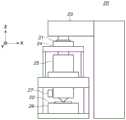
接下来,将详细描述根据本示例性实施例的曝光装置2的配置。曝光装置2包括完全覆盖曝光装置2的腔室4。腔室4在其中包括容纳了执行曝光处理的主体20的曝光单元5,以及从涂覆/显影装置3接收并向涂覆/显影装置3递送基板的基板传送设备(下文中称为第一传送设备)6。图2示意性地例示了安装在曝光单元5中的主体20的配置。主体20是投影曝光装置,其采用步进重复法或步进扫描法执行投影曝光以将在掩模21上形成的图案转印到基板22上。将参考图2描述主体20,假设Z轴平行于投影光学系统25的光轴,并且在垂直于Z轴的平面内,Y轴垂直于纸表面并且X轴垂直于Y轴。主体20包括照明设备23、保持掩模21的掩模台24、投影光学系统25、保持基板22的基板台26和捕获掩模的图像的图像捕获单元27。Next, the configuration of the
照明设备23包括光源和照明光学系统(均未示出)并且照射掩模21。作为光源,例如,使用脉冲光源(激光器)。可用的激光器的示例包括具有大约193nm波长的氟化氩(ArF)准分子激光器和具有大约153nm波长的分子氟(F2)准分子激光器。激光器的类型不限于准分子激光器,并且例如,可以使用钇铝石榴石(YAG)激光器。此外,激光器的数量没有特别限制。在使用激光器作为光源的情况下,期望使用将来自激光光源的平行光波束整形为期望波束形状的波束整形光学系统,或者使相干的激光波束不相干的不相干光学系统。此外,可用的光源不限于脉冲光源,并且也可以使用连续光源,诸如一个或多个汞灯或氙灯。照明光学系统包括透镜、反射镜、光积分器或光阑。The
掩模21是例如石英玻璃制的原板。要转印的图案(例如,电路图案)形成在掩模21上。掩模台24在保持掩模21的同时可在XY方向上移动。投影光学系统25将用来自照明设备23的曝光光照射的掩模21上的图案以预定倍率(例如,1/4或1/5)投影到基板22上。The
作为投影光学系统25,可以采用仅包括多个折射透镜元件的光学系统,或者包括多个折射透镜元件和至少一个凹面镜的光学系统(反射折射光学系统)。可替代地,作为投影光学系统25,可以采用包括多个折射透镜元件和至少一个衍射光学元件(诸如相息图(kinoform))的光学系统,或者全反射镜光学系统。As the projection
作为处理目标的基板22具有施加到表面的抗蚀剂并且例如由单晶硅形成。基板台26在保持基板22的同时可在XY方向上移动。例如,在采用步进扫描法的情况下,掩模台24和基板台26彼此同步地平行移动。The
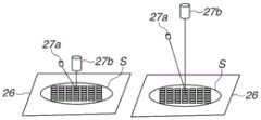
为了执行由基板台26保持的基板22的定位(对准),图像捕获单元27获取形成在基板22上的标记的捕获图像。图像捕获单元27包括发射光的光源27a(参考图14A)和接收被用从光源27a发射的光照射的图像捕获目标(基板22)反射的光并捕获图像捕获目标的图像的相机27b(参考图14A)。相机27b包括基于来自基板22的反射光的亮度(即,明暗)输出明暗图像的图像传感器(未示出)和将从图像传感器获得的明暗图像转换成数字图像信号的模数(A/D)转换器(未示出)。第一控制单元7(如下所述)获取数字图像信号,并使用获取的数字图像信号检测形成在基板22上的标记的位置。基于检测到的标记的位置,第一控制单元7控制基板台26执行基板22的定位。图像捕获单元27还可以获取形成在基板台26上的参考标记(未示出)的捕获图像,并且第一控制单元7还可以检测形成在基板台26上的参考标记的位置以执行基板台26的定位。In order to perform positioning (alignment) of the
第一传送设备6包括在曝光处理之前预先执行基板22的定位的预对准单元30,以及将基板22从预对准单元30供应给主体20中的基板台26的供应手31。第一传送设备6还包括载体端口32,作为在通过使用能够存储多个基板22的开放式盒将基板22直接搬入到主体20中的情况下放置开放式盒的部分。可替代地,载体端口32可以具有其中放置作为密封载体的前开门统一吊舱(FOUP)来代替开放式盒的结构。第一传送设备6还包括第一搬入单元33和第一搬出单元34,作为用于在曝光装置2和涂覆/显影装置3之间接收和递送基板22的第一接收/递送部分,以及适当地将基板22传送到第一传送设备6中包括的各个组件的传送手35。传送手35是例如选择顺应性装配机器手臂(SCARA,Selective Compliance AssemblyRobot Arm)机器人。第一搬入单元33是用于将处于未曝光状态的基板22从涂覆/显影装置3搬入曝光装置2中的接收/递送单元,但也可以用作预对准处理单元(诸如预对准单元30)或工艺处理单元(诸如温度调节单元)。另一方面,第一搬出单元34是用于将处于曝光状态的基板22从曝光装置2搬入涂覆/显影装置3中的接收/递送单元,但也可以用作工艺处理单元(诸如外围曝光处理单元)。The
此外,曝光装置2包括控制单元(下午中称为第一控制单元7),控制单元由例如计算机形成,通过线路连接到曝光装置2的组件,并且能够基于程序来控制组件。第一控制单元7可以一体地形成在曝光装置2内部,或者可以安装在与曝光装置2的其它部分分开的位置处。Furthermore, the
图3是例示信息处理装置300的配置的图。第一控制单元7可以通过可通信地连接到涂覆/显影装置3的信息处理装置(计算机)300实现。在图3中,处理单元301是执行操作系统(OS)和各种应用程序的中央处理单元(CPU)。处理单元301不限于CPU,并且可以是诸如微处理单元(MPU)、图形处理单元(GPU)或专用集成电路(ASIC)之类的处理器或电路。可替代地,处理单元301可以是诸如数字信号处理器(DSP)、数据流处理器(DFP)或神经处理单元(NPU)之类的处理器或电路。又可替代地,处理单元301可以是任何这些处理器或电路的组合。只读存储器(ROM)302存储要由处理单元301执行的程序和用于计算的参数当中的固定数据。随机存取存储器(RAM)303为处理单元301提供工作区域和用于临时存储数据的区域。ROM 302和RAM 303经由总线308连接到处理单元301。信息处理装置300还包括包含鼠标和键盘的输入设备(输入单元)305,以及诸如阴极射线管(CRT)或液晶显示器之类的显示设备(显示单元)306。可替代地,输入设备305和显示设备306可以是诸如触摸面板之类的集成设备。又可替代地,输入设备305和显示设备306可以与信息处理装置300分开配置。信息处理装置300还包括诸如硬盘设备、压缩盘(CD)、数字多功能盘(DVD)或存储卡之类的存储设备304。存储设备304存储各种程序和各种类型的数据。输入设备305、显示设备306和存储设备304中的每一个经由接口(未示出)连接到总线308。用于连接到网络并执行通信的通信设备307也连接到总线308。通信设备307被用于例如连接到局域网(LAN)、根据诸如传输控制协议/网际协议(TCP/IP)之类的通信协议执行数据通信,并与另一个通信设备进行通信。通信设备307用作数据传输单元和数据接收单元。例如,通信设备307从涂覆/显影装置3接收数据并将数据存储在存储设备304中。FIG. 3 is a diagram illustrating the configuration of the
<涂覆/显影装置><Coating/Developing Device>
接下来,将详细描述根据本示例性实施例的涂覆/显影装置3的配置。如图1中所示,涂覆/显影装置3包括安装在腔室40中的涂覆/显影处理单元8和安装在腔室41中并从曝光装置2接收基板22并将基板22递送到曝光装置2的基板传送设备(下文中称为第二传送设备)9。涂覆/显影处理单元8包括涂覆单元44、加热单元45、显影单元46和冷却单元47作为用于基板22的工艺处理单元。涂覆单元44例如采用旋涂机。涂覆单元44在抗蚀剂滴在水平放置的基板22的表面上的状态下旋转基板22,从而在上面形成均匀的抗蚀剂膜。加热单元45在曝光处理之前对基板22执行预烘烤,并对经受曝光处理的基板22执行曝光后烘烤。预烘烤是为了在向基板22的表面施加抗蚀剂之后蒸发抗蚀剂膜中的残留溶剂并增加抗蚀剂膜与基板22的表面之间的粘着而要执行的热处理。由于预烘烤是在未曝光状态下(曝光处理之前)对基板22执行的,因此期望预烘烤应当以聚合物处理中不发生聚合或添加剂不会热分解的温度执行。另一方面,曝光后烘烤是在曝光处理之后和显影处理之前要对基板22执行的热处理,以便减少在用单一波长的光曝光基板22的情况下由于驻波效应引起的抗蚀剂图案的变形。此外,曝光后烘烤具有促进化学放大的抗蚀剂在曝光后的催化反应的效果。作为用于由加热单元45执行的烘烤处理的方法,可以采用电阻加热法或红外线加热法。Next, the configuration of the coating/developing
显影单元46对经受曝光处理的基板22进行显影。作为用于由显影单元46执行的显影处理的方法,可以采用旋转法或喷射法。冷却单元47采用例如通过冷却水的循环而冷却的冷却板并且冷却处于加热状态的基板22。作为用于由冷却单元47执行的冷却处理的另一种方法,还可以采用利用Peltier效应的电子冷却。此外,涂覆/显影处理单元8包括作为放置诸如开放式盒或FOUP之类的载体的部分的载体端口48,以及在载体和工艺处理单元之间适当地传送基板22的传送手49。传送手49是例如SCARA机器人。这种开放式盒或FOUP可以在洁净室中由人引导车辆(PGV)传送,并被自动搬入和搬出载体端口48。可替代地,可以使用其中通过高架起重机运输(OHT)在洁净室中从上方将开放式盒或FOUP放置在载体端口48中的配置。The developing
第二传送设备9包括第二搬入单元50和第二搬出单元51作为用于在曝光装置2和涂覆/显影装置3之间接收和递送基板22的第二接收/递送部分。第二传送设备9还包括在第二搬入单元50和第二搬出单元51与安装在第一传送设备6中的第一搬入单元33和第一搬出单元34之间适当地传送基板22的传送手52。传送手52是例如SCARA机器人。第二搬入单元50是用于将经受曝光处理的基板22从曝光装置2搬出到涂覆/显影处理单元8中的接收/递送单元。另一方面,第二搬出单元51是用于将处于未曝光状态的基板22从涂覆显影处理单元8搬出到曝光装置2中的接收/递送单元。The second conveying
此外,涂覆/显影装置3包括控制单元(下文中称为第二控制单元10),该控制单元由例如计算机形成,通过线路连接到涂覆/显影装置3的组件,并且能够基于程序来控制组件。类似于第一控制单元7,第二控制单元10由例如图3中所示的信息处理装置300形成。第二控制单元10可以一体地形成在涂覆/显影装置3内部,或者可以安装在与涂覆/显影装置3的其它部分分开的位置处。Further, the coating/developing
接下来,将描述曝光装置2和涂覆/显影装置3的处理操作。在以下的描述中,假设一批25片基板22作为处理目标存储在开放式盒中,并传送到涂覆/显影装置3中的涂覆/显影处理单元8的载体端口48。首先,在涂覆/显影处理单元8中,传送手49从放置在载体端口48中的开放式盒中获取基板22并将基板22传送到涂覆单元44。涂覆单元44将抗蚀剂施加到搬入涂覆单元44中的各个基板22。然后,传送手49将具有施加到其的抗蚀剂的基板22从涂覆单元44搬出并将基板22传送到加热单元45。加热单元45对基板22执行预烘烤处理。在完成对基板22的预烘烤处理之后,传送手49将基板22从加热单元45搬出并将基板22传送到冷却单元47。冷却单元47对基板22执行冷却处理。此时,期望将稍后将搬入曝光装置2中的基板22的温度调整到不影响曝光装置2的腔室4内部的温度,即,主体20中的空调系统温度,作为目标温度。在根据本示例性实施例的曝光装置2中,如果温度调整单元安装在第一传送设备6中的第一搬入单元33中,那么从涂覆/显影装置3搬出到曝光装置2中的基板22的温度可以在曝光装置2中进行最终微调。在这种情况下,在冷却单元47中,可以使基板22的温度在一定程度上接近目标温度,并且可以稍微高于最终目标温度。接下来,传送手49将冷却至期望的目标温度的基板22搬出冷却单元47并将基板22传送到第二搬出单元51。如上所述,传送手49依次获取存储在开放式盒中的基板22并将基板22传送到工艺处理单元。第二传送设备9中的传送手52将由第二搬出单元51保持的基板22传送到曝光装置2中的第一传送设备6中的第一搬入单元33。Next, the processing operations of the
接下来,在另一侧的第一传送设备6中,第一搬入单元33通过使用第一搬入单元33内部的温度调整单元将基板22的温度调整到如上所述的预定温度。在完成对基板22的温度调整之后,传送手35将基板22从第一搬入单元33搬出并将基板22传送到预对准单元30。在预对准单元30中,基板22被放置在预对准单元30内部的台上并且由驱动系统(未示出)旋转。此时,诸如电荷耦合器件(CCD)传感器之类的检测器检测基板22的边缘部分。基于来自检测器的输出,第一控制单元7计算凹口的方向、基板22的中心和偏心量。然后,预对准单元30将形成在基板22中的凹口部分的方向最终调整到预定方向。在完成对基板22的预对准处理之后,供应手31将基板22从预对准单元30搬出并将基板22供应给主体20中的基板台26。主体20对基板22执行曝光处理。Next, in the
在完成对基板22的曝光处理之后,传送手35从基板台26获取经受了曝光处理的基板22并将基板22传送到第一搬出单元34。第二传送设备9中的传送手52将基板22从第一搬出单元34传送到第二搬入单元50。随后,涂覆/显影处理单元8中的传送手49将基板22从第二搬入单元50传送到加热单元45。加热单元45对搬入到加热单元45中的基板22执行曝光后烘烤处理。在完成对基板22的曝光后烘烤处理之后,传送手49将基板22从加热单元45搬出并将基板22传送到显影单元46。显影单元46对基板22执行显影处理。在完成对基板22的显影处理之后,传送手49将基板22从显影单元46搬出到放置在载体端口48中的开放式盒的预定槽中。After the exposure process on the
在根据本示例性实施例的检查处理中,首先,准备要用于检查的基板(下文中称为检查基板S)。检查基板S被传送到涂覆/显影装置3并经受涂覆/显影装置3的涂覆处理,使得在检查基板S上形成抗蚀剂膜。上面形成有抗蚀剂膜的检查基板S被传送到曝光装置2,并经受曝光装置2的曝光处理,使得抗蚀剂膜被曝光。此时,在没有上面形成有图案的掩模的情况下,曝光装置2在改变曝光量的同时依次对检查基板S上的多个检查区域进行曝光。经受了曝光处理的检查基板S被再次传送到涂覆/显影装置3并经受涂覆/显影装置3的显影处理,使得检查基板S上的抗蚀剂膜的一部分被移除。In the inspection process according to the present exemplary embodiment, first, a substrate to be used for inspection (hereinafter referred to as inspection substrate S) is prepared. The inspection substrate S is conveyed to the coating/developing
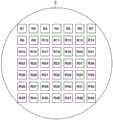
图4是例示检查基板S上的检查区域的图。在图4的示例中,检查区域R1至R49形成在检查基板S上。但是,检查区域的尺寸、数量和位置不限于这个示例。在曝光处理中,以不同的曝光量依次曝光检查区域R1至R49。FIG. 4 is a diagram illustrating an inspection area on the inspection substrate S. FIG. In the example of FIG. 4 , the inspection regions R1 to R49 are formed on the inspection substrate S. In the example of FIG. However, the size, number and position of the inspection areas are not limited to this example. In the exposure process, the inspection regions R1 to R49 are sequentially exposed with different exposure amounts.
如果曝光处理中的曝光量不足,那么对检查区域执行的显影处理不充分,并且抗蚀剂膜会部分地残留在检查区域中。图5例示了多个检查区域的显影状态。更具体而言,图5的示例例示了检查区域R1至R4的显影状态。图5还例示了在曝光处理中按照检查区域R1至R4的次序增加曝光量的示例。检查区域R1至R4的曝光量分别是E1至E4。在以曝光量E1至E4当中的最小曝光量E1曝光的检查区域R1中,抗蚀剂膜在整个区域上残留。在以第二小曝光量E2曝光的检查区域R2中,抗蚀剂膜部分地残留在四个角处及其周围。在以第三小曝光量E3曝光的检查区域R3中,抗蚀剂膜部分地残留在四个角处及其周围。检查区域R3的抗蚀剂膜残留的部分比检查区域R2的抗蚀剂膜残留的部分小。在以曝光量E1至E4当中的最大曝光量E4曝光的检查区域R4中,抗蚀剂膜被从整个区域去除并且完全不残留。If the exposure amount in the exposure process is insufficient, the development process performed on the inspection area is insufficient, and the resist film may partially remain in the inspection area. FIG. 5 illustrates the development state of a plurality of inspection regions. More specifically, the example of FIG. 5 illustrates the development states of the inspection regions R1 to R4 . FIG. 5 also illustrates an example in which the exposure amount is increased in the order of the inspection regions R1 to R4 in the exposure processing. The exposure amounts of the inspection regions R1 to R4 are E1 to E4, respectively. In the inspection region R1 exposed with the smallest exposure amount E1 among the exposure amounts E1 to E4, the resist film remains on the entire region. In the inspection region R2 exposed with the second small exposure amount E2, the resist film partially remains at and around the four corners. In the inspection region R3 exposed with the third small exposure amount E3, the resist film partially remains at and around the four corners. The portion where the resist film remains in the inspection region R3 is smaller than the portion where the resist film remains in the inspection region R2. In the inspection region R4 exposed with the maximum exposure amount E4 among the exposure amounts E1 to E4, the resist film is removed from the entire region and does not remain at all.
以上描述是基于抗蚀剂膜的在曝光处理中被曝光的部分在显影处理中被去除的前提。如果抗蚀剂膜由正抗蚀剂形成,那么抗蚀剂膜的在曝光处理中被曝光的部分在显影处理中被去除。另一方面,如果抗蚀剂膜由负抗蚀剂形成,那么抗蚀剂膜的在曝光处理中被曝光的部分以外的部分在显影处理中被去除。在抗蚀剂膜由负抗蚀剂形成的情况下,图5例示了按照检查区域R1至R4的次序减少曝光量的示例。The above description is based on the premise that the portion of the resist film exposed in the exposure process is removed in the development process. If the resist film is formed of a positive resist, the portion of the resist film exposed in the exposure process is removed in the development process. On the other hand, if the resist film is formed of a negative resist, a portion of the resist film other than the portion exposed in the exposure process is removed in the development process. In the case where the resist film is formed of a negative resist, FIG. 5 illustrates an example in which the exposure amount is reduced in the order of the inspection regions R1 to R4 .
如上所述,检查在检查基板S上的检查区域R1至R4中的每一个中的显影的抗蚀剂膜的残留状态(下文中称为显影状态),由此可以获取检查基板S上的检查区域R1至R4中显影状态与曝光量E1至E4之间的关系。As described above, the residual state of the developed resist film (hereinafter referred to as the developed state) in each of the inspection regions R1 to R4 on the inspection substrate S is inspected, whereby the inspection on the inspection substrate S can be acquired The relationship between the development state and the exposure amounts E1 to E4 in the regions R1 to R4.
常规地,为了确定检查基板S上的检查区域中的显影状态,具有技术知识和经验的人通过使用扫描电子显微镜(SEM)或光学显微镜来观察检查基板S上的检查区域。在多个人执行检查的情况下,用于确定检查区域中抗蚀剂膜是否被去除到适当水平的准则取决于执行检查的人而不同,并且在确定结果中发生变化。Conventionally, in order to determine the development state in the inspection area on the inspection substrate S, a person with technical knowledge and experience observes the inspection area on the inspection substrate S by using a scanning electron microscope (SEM) or an optical microscope. In the case where inspection is performed by a plurality of persons, the criterion for determining whether the resist film in the inspection area is removed to an appropriate level differs depending on the persons who perform the inspection, and varies in the determination result.
为了解决这个问题,在根据本示例性实施例的检查处理中,检查基板S上的检查区域的图像被输入到通过机器学习而获得的学习模型,并且从学习模型中输出指示检查区域的显影状态的信息。In order to solve this problem, in the inspection process according to the present exemplary embodiment, the image of the inspection area on the inspection substrate S is input to a learning model obtained by machine learning, and the development state indicating the inspection area is output from the learning model Information.
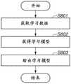
图6是例示由信息处理装置300执行的检查处理的图。根据本示例性实施例的检查处理由图3中所示的信息处理装置300执行。可替代地,根据本示例性实施例的检查处理可以由曝光装置2的第一控制单元7或涂覆/显影装置3的第二控制单元10执行,或者可以由另一个信息处理装置(未示出)执行。FIG. 6 is a diagram illustrating inspection processing performed by the
处理单元301包括学习单元201和检查单元202。学习单元201通过使用从存储设备304获取的学习数据211进行学习来获得学习模型213。The
学习数据211包括经受了显影处理的检查基板(第一基板)上的检查区域的捕获图像作为输入数据221。学习数据211还包括指示经受了显影处理的检查基板上的检查区域的显影状态的信息作为教师数据222。指示检查区域的显影状态的信息可以是指示检查区域的显影状态的数值信息。例如,关于图5中所示的检查区域R1至R4的显影状态,检查区域R1的显影状态可以被指示为0%,检查区域R2的显影状态可以被指示为33%,检查区域R3的显影状态可以被指示为66%,而检查区域R4的显影状态可以被指示为100%。The learning
可替代地,指示检查区域的显影状态的信息可以是指示检查区域的显影状态中的每一个是否可接受的信息。例如,关于图5中所示的检查区域R1至R4的显影状态,检查区域R1和R2的显影状态可以被指示为不合格,而检查区域R3和R4的显影状态可以被指示为合格。学习数据211是包括输入数据221和教师数据222的多个组合的信息。例如,基于由观察输入数据221中包括的检查区域的图像的人对检查区域的显影状态的检查的结果,获取教师数据222中包括的指示检查区域的显影状态的信息。Alternatively, the information indicating the development states of the inspection areas may be information indicating whether each of the development states of the inspection areas is acceptable. For example, with regard to the development states of the inspection regions R1 to R4 shown in FIG. 5 , the development states of the inspection regions R1 and R2 may be indicated as failed, and the development states of the inspection regions R3 and R4 may be indicated as acceptable. The learning
基于经受了显影处理的检查基板上的检查区域的图像,显影处理中抗蚀剂膜被去除的部分与抗蚀剂膜残留的部分可以彼此区分,如图5中所示。在抗蚀剂膜由正抗蚀剂形成的情况下,抗蚀剂膜被去除的部分越大,显影状态越好。另一方面,在抗蚀剂膜由负抗蚀剂形成的情况下,抗蚀剂膜被去除的部分以外的部分越大,显影状态越好。经受了显影处理的检查基板上的检查区域的图像与检查区域的显影状态相关。如上所述,检查区域的显影状态也与曝光处理中的曝光量存在关系。因此,经受了显影处理的检查基板上的检查区域的图像也与曝光处理中的曝光量相关。Based on the image of the inspection area on the inspection substrate subjected to the development process, the portion where the resist film is removed in the development process and the portion where the resist film remains can be distinguished from each other, as shown in FIG. 5 . In the case where the resist film is formed of a positive resist, the larger the portion where the resist film is removed, the better the development state. On the other hand, when the resist film is formed of a negative resist, the larger the portion other than the portion from which the resist film is removed, the better the development state. The image of the inspection area on the inspection substrate subjected to the development process is related to the development state of the inspection area. As described above, the development state of the inspection area also has a relationship with the exposure amount in the exposure process. Therefore, the image of the inspection area on the inspection substrate subjected to the development process is also related to the exposure amount in the exposure process.
图7A和图7B分别例示了学习单元201和检查单元202中的数据流。学习单元201通过使用指示输入数据221与教师数据222之间的关系的学习数据211执行机器学习来获得学习模型213。然后,检查单元202向获得的学习模型213输入新的输入数据212,从而输出检查数据214作为输出数据。7A and 7B illustrate the data flow in the
学习模型213可以由例如神经网络形成。在此神经网络是指具有包括输入层、中间层和输出层的多层网络结构的模型。学习模型213不一定由神经网络形成,并且可以由诸如支持向量机之类的另一种模型形成。学习模型213可以包括通过使用指示输入数据221与检查数据214之间的关系的表或多项式来获取输入数据221和检查数据214的模型。The
接下来将描述由学习单元201执行的学习处理。图8是例示由学习单元201执行的学习处理的流程图。在步骤S801中,学习单元201从存储设备304获取学习数据211。学习单元201可以从RAM303获取学习数据211,或者可以经由通信设备307获取保存在外部存储设备(未示出)中的学习数据211。Next, the learning process performed by the
在步骤S802中,学习单元201执行机器学习以获得学习模型213。例如,在学习模型213由神经网络形成的情况下,学习单元201通过使用诸如反向传播之类的算法来获得学习模型213。学习单元201通过优化神经网络中的连接加权系数来获得学习模型213。反向传播是一种用于调整各个神经网络的节点之间的连接加权系数以使输出数据与教师数据222之间的误差最小化的技术。In step S802 , the
图7A例示了当学习单元201执行机器学习以获得学习模型213时数据是如何流动的。学习单元201基于输入到输入层的输入数据221获得教师数据222与从神经网络的输出层输出的检查数据214之间的误差。使用损失函数215,学习单元201计算来自神经网络的检查数据214与教师数据222之间的误差。基于获得的误差,学习单元201更新神经网络的节点之间的连接加权系数,以使误差小于预定的允许值,从而获得对其应用了更新后的连接加权系数的学习模型213。FIG. 7A illustrates how data flows when the
在步骤S803中,学习单元201将在步骤S802中获得的学习模型213输出到检查单元202。学习单元201可以将学习模型213保存在存储设备304中,并且检查单元202可以获取保存的学习模型213。可替代地,学习模型213可以保存在RAM 303中,或者可以经由通信设备307保存在外部存储设备(未示出)中。In step S803 , the
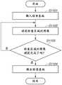
接下来将描述由检查单元202执行的检查处理。图9是例示由检查单元202执行的检查处理的流程图。在步骤S901中,检查单元202从存储设备304获取输入数据212。此时,检查单元202可以从RAM 303获取输入数据212,或者可以经由通信设备307获取保存在外部存储设备(未示出)中的输入数据212。输入数据212包括检查基板(第二基板)上的检查区域的捕获图像。输入数据212的细节与包括在学习数据211中的输入数据221的细节相似。Next, the inspection processing performed by the
在步骤S902中,检查单元202从学习单元201获得学习模型213。检查单元202可以从RAM 303获得学习模型213,或者可以经由通信设备307获得保存在外部存储设备(未示出)中的学习模型213。In step S902 , the
在步骤S903中,检查单元202将在步骤S901中获取的输入数据212输入到在步骤S902中获得的学习模型213,从而获取从学习模型213输出的检查数据214。检查数据214包括指示经受了显影处理的检查基板上的检查区域的显影状态的信息。指示检查区域的显影状态的信息可以是指示检查区域的显影状态的数值信息。可替代地,指示检查区域的显影状态的信息可以是指示检查区域的显影状态中的每一个是否可接受的信息。检查数据214的细节与学习数据211中包括的教师数据222的细节相似。检查单元202将检查数据214保存在存储设备304中。可替代地,检查数据214可以保存在RAM 303中,或者可以经由通信设备307保存在外部存储设备(未示出)中。In step S903 , the
图7B例示了当检查单元202获取检查数据214时数据如何流动。检查单元202基于输入到学习模型213的输入数据212来获取从学习模型213输出的检查数据214。例如,在学习模型213由神经网络形成的情况下,获取基于输入到输入层的输入数据212并基于节点之间的连接加权系数而从输出层输出的检查数据214。FIG. 7B illustrates how the data flows when the
在步骤S904中,检查单元202将在步骤S903中获取的检查数据214输出到显示设备306。In step S904 , the
显示设备306在画面上显示从检查单元202输出的检查数据214。图10例示了由显示设备306显示的画面400。画面400包括显示区域401和显示区域402,显示区域401显示输入数据212中包括的检查基板上的检查区域的捕获图像,而显示区域402显示检查数据214中包括的指示经受了显影处理的检查基板上的检查区域的显影状态的信息。图10例示了其中指示检查区域的显影状态的数值信息被显示为指示经受了显影处理的检查基板上的检查区域的显影状态的信息的示例。但是,指示经受了显影处理的检查基板上的检查区域的显影状态的信息不限于此。例如,可以在显示区域402上显示指示检查区域的各个显影状态是否可接受的信息,作为指示经受了显影处理的检查基板上的检查区域的显影状态的信息。可替代地,在显示区域402上,可以显示指示检查区域的各个显影状态的数值信息,并且指示检查区域的各个显影状态的数值信息的背景颜色、文本颜色和字体中的至少一个可以被改变以显示指示检查区域的各个显影状态是否可接受的信息。The
现在将描述用于获取包括在输入数据221和输入数据212中的每一个中的经受了显影处理的检查基板上的检查区域的捕获图像的方法。图11是例示对检查区域的图像捕获处理的流程图。将参考图11描述曝光装置2对检查区域执行图像捕获处理的示例。可替代地,图像捕获处理可以由包括图像捕获单元的另一个装置(未示出)(诸如检查基板的检查装置)执行。将参考图11描述使用用于捕获形成在基板22上的标记的图像的图像捕获单元27的示例。可替代地,可以使用放置在曝光装置2中的另一个图像捕获单元(未示出)。A method for acquiring a captured image of an inspection area on an inspection substrate subjected to development processing included in each of the
在步骤S1101中,曝光装置2的第一控制单元7使第一传送设备6将检查基板S传送到基板台26。此时,检查基板S已经经受了直到显影处理的处理。In step S1101 , the first control unit 7 of the
在步骤S1102中,第一控制单元7移动基板台26,使得检查基板S上的检查区域位于图像捕获单元27的成像区域中。然后,第一控制单元7使图像捕获单元27捕获检查基板S上的检查区域的图像。第一控制单元7将检查基板S上的检查区域的捕获图像的图像数据保存在存储设备304中。可替代地,第一控制单元7可以将检查基板S上的检查区域的捕获图像的图像数据保存在RAM 303中或经由通信设备307保存在外部存储设备(未示出)中。In step S1102 , the first control unit 7 moves the
可以可选地设置用于捕获检查基板S上的检查区域的图像的成像区域。例如,可以设置成像区域以完全包括图4中所示的检查基板S。可替代地,如图5中所示,可以设置成像区域以包括所有检查区域中的一些。以这种方式,可以设置宽的成像区域以一次获取包括多个检查区域的图像,并且这使得可以缩短用于图像捕获处理的时间。An imaging area for capturing an image of the inspection area on the inspection substrate S may optionally be provided. For example, the imaging area may be set to completely include the inspection substrate S shown in FIG. 4 . Alternatively, as shown in FIG. 5, the imaging area may be set to include some of all inspection areas. In this way, a wide imaging area can be set to acquire an image including a plurality of inspection areas at one time, and this makes it possible to shorten the time for image capturing processing.
可替代地,如图12中所示,可以设置成像区域R0以包括单个检查区域R1。以这种方式,可以设置比包括多个检查区域的成像区域窄的成像区域以获取高清晰图像,并且这使得可以提高检查准确度。Alternatively, as shown in FIG. 12, the imaging region R0 may be set to include a single examination region R1. In this way, an imaging area narrower than an imaging area including a plurality of inspection areas can be set to acquire a high-definition image, and this makes it possible to improve inspection accuracy.
又可替代地,如图13中所示,可以为单个检查区域R1设置多个成像区域R0。以这种方式,可以设置甚至更窄的成像区域来获取高清晰图像,并且这使得可以进一步提高检查准确度。此时,期望的是包括矩形检查区域R1的四个角的区域应当被设置为成像区域R0。这是因为,如图5中的检查区域R2和R3中所示,抗蚀剂膜残留在四个角处。将包括四个角的区域设置为成像区域R0使得可以更准确地确定取决于曝光量抗蚀剂膜是否残留。Still alternatively, as shown in FIG. 13 , a plurality of imaging regions R0 may be provided for a single inspection region R1 . In this way, an even narrower imaging area can be set to acquire a high-definition image, and this makes it possible to further improve the inspection accuracy. At this time, it is desirable that an area including the four corners of the rectangular inspection area R1 should be set as the imaging area R0. This is because, as shown in the inspection regions R2 and R3 in FIG. 5 , the resist film remains at the four corners. Setting the area including the four corners as the imaging area R0 makes it possible to more accurately determine whether the resist film remains depending on the exposure amount.
图像捕获单元27可以在改变用于捕获检查基板S上的检查区域的图像的成像条件的同时获取多个图像。图14A至图14D例示了由图像捕获单元27对检查基板S的图像捕获。更具体而言,图14A例示了其中图像捕获单元27的光源27a将光发射到由基板台26保持的检查基板S上的检查区域,并且相机27b接收在检查区域上反射的光并捕获检查区域的图像的状态。The
图14B例示了其中图像捕获单元27在改变作为成像条件的基板台26的角度的同时捕获检查区域的图像的状态。图像捕获单元27可以在将多个角度设置为基板台26的角度的同时执行图像捕获,从而获取单个检查区域的多个图像。FIG. 14B illustrates a state in which the
图14C例示了其中图像捕获单元27在改变作为成像条件的从图像捕获单元27到检查基板S上的检查区域的距离的同时捕获检查区域的图像的状态。图像捕获单元27可以在将多个距离设置为到检查区域的距离的同时执行图像捕获,从而获取单个检查区域的多个图像。可替代地,可以改变从图像捕获单元27的光源27a和相机27b中的至少一个到检查基板S上的检查区域的距离。又可替代地,在相机27b具有焦距改变功能的情况下,可以改变相机27b的焦距而不是改变从图像捕获单元27到检查区域的距离。14C illustrates a state in which the
图14D例示了其中图像捕获单元27在改变作为成像条件的照明条件(诸如从光源27a发射的光的波长或光量)的同时捕获检查区域的图像的状态。图像捕获单元27可以在将多个照明条件设置为照明条件的同时执行图像捕获,从而获取单个检查区域的多个图像。FIG. 14D illustrates a state in which the
如上所述,可以获取单个检查区域的多个图像。因而,学习单元201可以利用增加数量的学习数据211来获得学习模型213。这提高了由从获得的学习模型213输出的检查数据214所指示的检查结果的准确度。此外,检查单元202可以利用增加数量的输入数据212来获取检查数据214。这使得可以获取多条检查数据214并使用多条检查数据214执行检查。因此,提高了检查结果的准确度。作为成像条件,基板台26的角度、到检查区域的距离和照明条件中的至少两个可以被组合在一起,并且图像捕获单元27可以在改变成像条件的同时捕获检查区域的图像。As mentioned above, multiple images of a single inspection area can be acquired. Thus, the
返回到图11的描述,在步骤S1103中,第一控制单元7确定是否完成对检查基板S上的检查区域的图像捕获。在其中预先设置了多个检查区域的图像捕获的情况下,或者在其中预先设置了在多个捕获条件下的图像捕获的情况下,第一控制单元7重复图像捕获。如果第一控制单元7确定未完成对检查基板S上的检查区域的图像捕获(步骤S1103中的“否”),那么处理返回到步骤S1102。如果第一控制单元7确定完成了对检查基板S上的检查区域的图像捕获(步骤S1103中的“是”),那么处理前进到步骤S1104。Returning to the description of FIG. 11 , in step S1103 , the first control unit 7 determines whether image capturing of the inspection area on the inspection substrate S is completed. The first control unit 7 repeats the image capturing in a case where image capturing of a plurality of inspection regions is set in advance, or in a case where image capturing under a plurality of capturing conditions is preset. If the first control unit 7 determines that the image capturing of the inspection area on the inspection substrate S is not completed (NO in step S1103 ), the process returns to step S1102 . If the first control unit 7 determines that the image capturing of the inspection area on the inspection substrate S is completed (YES in step S1103 ), the process proceeds to step S1104 .
在步骤S1104中,第一控制单元7使第一传送设备6从基板台26搬出检查基板S。In step S1104 , the first control unit 7 causes the
如上所述,根据本示例性实施例的信息处理装置300能够将基板的图像输入到学习模型213以获取指示基板的显影状态的信息,从而使得可以检查经受了显影处理的基板的显影状态。As described above, the
接下来,将描述根据第二示例性实施例的信息处理装置。本示例性实施例中未提及的项与第一示例性实施例一致。在本示例性实施例中,基于在图9的流程图中的步骤S903中获取的检查数据214,检查单元202确定曝光装置2要对基板22进行曝光的曝光量。Next, the information processing apparatus according to the second exemplary embodiment will be described. Items not mentioned in this exemplary embodiment are consistent with the first exemplary embodiment. In the present exemplary embodiment, based on the
图15是例示曝光量确定处理的流程图。在步骤S1501中,检查单元202从存储设备304获取检查数据214。如第一示例性实施例中所述,检查数据214包括指示检查区域的显影状态的信息。例如,指示检查区域的显影状态的信息可以是指示检查区域的显影状态的数值信息或指示检查区域的各个显影状态是否可接受的信息。FIG. 15 is a flowchart illustrating exposure amount determination processing. In step S1501 , the
在步骤S1502中,检查单元202确定获取的检查数据214是否可接受。例如,在检查数据214包括指示检查区域的各个显影状态的数值信息的情况下,检查单元202确定指示检查区域的显影状态的数值是否在预定的允许范围内。如果检查数据214包括指示检查区域的显影状态是否可接受(合格或不合格)的信息,那么检查单元202确定检查区域的显影状态是否可接受。In step S1502, the
在步骤S1503中,检查单元202获取与被确定为可接受的检查数据214对应的曝光量。例如,检查单元202从在步骤S1501中获取的检查数据214当中获取其中指示检查区域的显影状态的数值被确定为在预定的允许范围内的检查数据214,作为被确定为可接受的检查数据214。可替代地,例如,检查单元202获取其中检查区域的显影状态被确定为合格的检查数据214,作为被确定为可接受的检查数据214。接下来,检查单元202获取与被确定为可接受的检查数据214对应的输入数据221中包括的图像中的检查区域被曝光的曝光量。在此假设检查区域被曝光的曝光量与检查区域的图像一起预先存储在存储设备304中。In step S1503, the
在步骤S1504中,基于在步骤S1503中获取的曝光量,检查单元202确定由曝光装置2对基板22进行曝光的曝光量。在获取多条检查数据214作为被确定为可接受的检查数据214的情况下,检查单元202将所获取的多个曝光量中的最小曝光量确定作为由曝光装置2对基板22进行曝光的曝光量。In step S1504 , based on the exposure amount acquired in step S1503 , the
如上所述,根据本示例性实施例的信息处理装置能够将基板的图像输入到学习模型213以获取指示基板的显影状态的信息,从而使得可以检查经受了显影处理的基板的显影状态。此外,基于经受了显影处理的基板的显影状态的检查结果,可以确定由曝光装置2对基板22进行曝光的曝光量。As described above, the information processing apparatus according to the present exemplary embodiment can input the image of the substrate to the
接下来,将描述根据第三示例性实施例的信息处理装置。本示例性实施例中未提及的项与第一示例性实施例一致。在本示例性实施例中,基于在图9的步骤S903中获取的检查数据214,检查单元202获取用于检查曝光装置2中是否发生耀斑的检查数据214。Next, the information processing apparatus according to the third exemplary embodiment will be described. Items not mentioned in this exemplary embodiment are consistent with the first exemplary embodiment. In the present exemplary embodiment, based on the
图16例示了在发生耀斑的状态下曝光的检查区域R1的捕获图像。例如,在发生耀斑的状态下由曝光装置2对检查区域R1进行曝光的情况下,在经受了显影处理的检查基板S上的检查区域R1的捕获图像中出现独特的图案,如图16中所示。FIG. 16 illustrates a captured image of the inspection region R1 exposed in a state where a flare has occurred. For example, in the case where the inspection region R1 is exposed by the
考虑到以上问题,作为指示检查区域R1的显影状态的信息,指示在检查基板S的曝光期间是否发生了耀斑的信息被包括在学习数据211的教师数据222中。这使得由学习单元201获得的学习模型213能够输出指示是否发生了耀斑的信息作为检查数据214。因而,当检查单元202将包括检查基板S上的检查区域R1的捕获图像的输入数据212输入到学习模型213时,检查单元202可以获取包括指示是否在检查基板S的曝光期间发生了耀斑的信息的检查数据214。In consideration of the above problem, as information indicating the development state of the inspection region R1 , information indicating whether flare occurred during exposure of the inspection substrate S is included in the
如上所述,根据本示例性实施例的信息处理装置能够将基板的图像输入到学习模型213以检查在基板的曝光期间是否发生了耀斑。As described above, the information processing apparatus according to the present exemplary embodiment can input the image of the substrate to the
接下来,将描述根据第四示例性实施例的信息处理装置。本示例性实施例中未提及的项与第一示例性实施例一致。在本示例性实施例中,基于在图9的步骤S903中获取的检查数据214,检查单元202获取用于检查曝光装置2中包括的光学元件是否发生异常的检查数据214。Next, the information processing apparatus according to the fourth exemplary embodiment will be described. Items not mentioned in this exemplary embodiment are consistent with the first exemplary embodiment. In the present exemplary embodiment, based on the
图17例示了在光学元件中发生异常的状态下曝光的检查区域R1的捕获图像。例如,在曝光装置2中包括的光学元件中存在划痕的状态下或者在异物附着到光学元件的状态下对检查区域R1进行曝光的情况下,具有独特形状的区域出现在经受了显影处理的检查基板S上的检查区域R1的捕获图像中,如图17中所示。曝光装置2中包括的光学元件的示例包括曝光装置2的照明设备23和投影光学系统25中包括的光学元件。FIG. 17 illustrates a captured image of the inspection region R1 exposed in a state where an abnormality has occurred in the optical element. For example, in the case where the inspection region R1 is exposed in a state where scratches are present in the optical element included in the
考虑到上述问题,作为指示检查区域R1的显影状态的信息,指示光学元件中是否发生异常的信息被包括在学习数据211的教师数据222中。这使得由学习单元201获得的学习模型213能够输出指示光学元件中是否发生异常的信息作为检查数据214。因而,当检查单元202将包括检查基板S上的检查区域R1的捕获图像的输入数据212输入到学习模型213时,检查单元202可以获取包括指示光学元件中是否发生异常的信息的检查数据214。In consideration of the above-mentioned problem, as the information indicating the development state of the inspection region R1 , information indicating whether an abnormality has occurred in the optical element is included in the
如上所述,根据本示例性实施例的信息处理装置能够将基板的图像输入到学习模型213以检查在已经曝光基板的曝光装置2中包括的光学元件中是否发生异常。As described above, the information processing apparatus according to the present exemplary embodiment can input the image of the substrate to the
接下来将描述用于制造诸如器件(例如,半导体器件、磁存储介质或液晶显示器件)、滤色器或硬盘之类的物品的方法。物品制造方法包括使用曝光装置在基板(晶片、玻璃板或膜基板)上形成图案的工艺。物品制造方法还包括对上面形成有图案的基板进行处理的工艺。处理工艺包括去除图案的剩余膜的步骤。处理步骤还可以包括另一个已知步骤,诸如使用图案作为掩模蚀刻基板的步骤。根据本示例性实施例的物品制造方法在物品的性能、质量、生产率和生产成本中的至少一个方面优于常规方法。Next, methods for manufacturing articles such as devices (eg, semiconductor devices, magnetic storage media, or liquid crystal display devices), color filters, or hard disks will be described. The article manufacturing method includes a process of forming a pattern on a substrate (wafer, glass plate or film substrate) using an exposure device. The article manufacturing method also includes a process of treating the substrate on which the pattern is formed. The processing process includes the step of removing the remaining film of the pattern. The processing step may also include another known step, such as etching the substrate using the pattern as a mask. The article manufacturing method according to the present exemplary embodiment is superior to the conventional method in at least one of the performance, quality, productivity, and production cost of the article.
上述的第一示例性实施例至第四示例性实施例不仅能够单独执行,而且能够以其任何组合执行。The above-described first to fourth exemplary embodiments can be implemented not only individually but also in any combination thereof.
根据上述示例性实施例,可以提供能够检查基板的显影状态的信息处理装置、检查方法、存储介质、曝光装置、确定方法和物品制造方法。According to the above-described exemplary embodiments, it is possible to provide an information processing apparatus, an inspection method, a storage medium, an exposure apparatus, a determination method, and an article manufacturing method capable of inspecting the development state of a substrate.
本发明的(一个或多个)实施例还可以通过读出并执行记录在存储介质(其也可以被更完整地称为“非暂态计算机可读存储介质”)上的计算机可执行指令(例如,一个或多个程序)以执行上述(一个或多个)实施例中的一个或多个实施例的功能和/或包括用于执行上述(一个或多个)实施例中的一个或多个实施例的功能的一个或多个电路(例如,专用集成电路(ASIC))的系统或装置的计算机来实现,以及通过由系统或装置的计算机通过例如从存储介质读出并执行计算机可执行指令以执行上述(一个或多个)实施例中的一个或多个实施例的功能和/或控制一个或多个电路执行上述(一个或多个)实施例中的一个或多个实施例的功能而执行的方法来实现。计算机可以包括一个或多个处理器(例如,中央处理单元(CPU)、微处理单元(MPU)),并且可以包括单独计算机或单独处理器的网络,以读出并执行计算机可执行指令。计算机可执行指令可以例如从网络或存储介质提供给计算机。存储介质可以包括例如硬盘、随机存取存储器(RAM)、只读存储器(ROM)、分布式计算系统的存储设备、光盘(诸如紧凑盘(CD)、数字多功能盘(DVD)或蓝光盘(BD)TM)、闪存设备、存储卡等中的一个或多个。Embodiment(s) of the present invention may also be implemented by reading and executing computer-executable instructions ( For example, one or more programs) to perform the functions of and/or include functions for performing one or more of the above-described embodiment(s) The functions of the various embodiments are implemented by one or more circuits (eg, application specific integrated circuits (ASICs)) of a computer of a system or device, and executable by a computer of the system or device by reading and executing, for example, from a storage medium instructions to perform the functions of one or more of the above-described embodiment(s) and/or to control one or more circuits to perform the functions of one or more of the above-described embodiment(s) function to implement the method. A computer may include one or more processors (eg, central processing unit (CPU), micro processing unit (MPU)), and may include individual computers or a network of individual processors, to read and execute computer-executable instructions. Computer-executable instructions may be provided to the computer, eg, from a network or storage medium. The storage medium may include, for example, a hard disk, a random access memory (RAM), a read only memory (ROM), a storage device of a distributed computing system, an optical disk such as a compact disk (CD), a digital versatile disk (DVD), or a Blu-ray disk ( One or more of BD)™ ), flash memory devices, memory cards, etc.
本发明的实施例还可以通过如下的方法来实现,即,通过网络或者各种存储介质将执行上述实施例的功能的软件(程序)提供给系统或装置,该系统或装置的计算机或是中央处理单元(CPU)、微处理单元(MPU)读出并执行程序的方法。The embodiments of the present invention can also be implemented by the following method, that is, providing software (programs) for performing the functions of the above-mentioned embodiments to a system or device through a network or various storage media, and the computer of the system or device or the central A method in which a processing unit (CPU) and a micro processing unit (MPU) read and execute programs.
虽然已经参考示例性实施例描述了本公开,但是应该理解的是,本公开不限于所公开的示例性实施例。所附权利要求的范围应被赋予最广泛的解释以涵盖所有此类修改以及等同的结构和功能。While the present disclosure has been described with reference to exemplary embodiments, it should be understood that the present disclosure is not limited to the disclosed exemplary embodiments. The scope of the appended claims is to be accorded the broadest interpretation so as to encompass all such modifications and equivalent structures and functions.
Claims (15)
Applications Claiming Priority (2)
| Application Number | Priority Date | Filing Date | Title |
|---|---|---|---|
| JP2020162585AJP7596106B2 (en) | 2020-09-28 | 2020-09-28 | Information processing apparatus, inspection method, program, exposure apparatus, determination method, and article manufacturing method |
| JP2020-162585 | 2020-09-28 |
Publications (1)
| Publication Number | Publication Date |
|---|---|
| CN114326318Atrue CN114326318A (en) | 2022-04-12 |
Family
ID=80821117
Family Applications (1)
| Application Number | Title | Priority Date | Filing Date |
|---|---|---|---|
| CN202111118738.4APendingCN114326318A (en) | 2020-09-28 | 2021-09-24 | Information processing apparatus, inspection method, storage medium, exposure apparatus, determination method, and article manufacturing method |
Country Status (3)
| Country | Link |
|---|---|
| US (1) | US20220100081A1 (en) |
| JP (1) | JP7596106B2 (en) |
| CN (1) | CN114326318A (en) |
Cited By (1)
| Publication number | Priority date | Publication date | Assignee | Title |
|---|---|---|---|---|
| CN114706281A (en)* | 2022-05-18 | 2022-07-05 | 圆周率半导体(南通)有限公司 | Method for improving exposure uniformity of PCB |
Citations (3)
| Publication number | Priority date | Publication date | Assignee | Title |
|---|---|---|---|---|
| CN1488999A (en)* | 2002-08-30 | 2004-04-14 | 株式会社东芝 | Inspection method of exposure device and exposure device |
| CN104884945A (en)* | 2012-12-27 | 2015-09-02 | 株式会社尼康 | Inspection apparatus, inspection method, exposure system, exposure method, and device manufacturing method |
| US20170177760A1 (en)* | 2015-12-17 | 2017-06-22 | Asml Netherlands B.V. | Optical metrology of lithographic processes using asymmetric sub-resolution features to enhance measurement |
Family Cites Families (2)
| Publication number | Priority date | Publication date | Assignee | Title |
|---|---|---|---|---|
| JP7137943B2 (en)* | 2018-03-20 | 2022-09-15 | 株式会社日立ハイテク | SEARCHING DEVICE, SEARCHING METHOD AND PLASMA PROCESSING DEVICE |
| KR102711835B1 (en)* | 2019-04-04 | 2024-10-02 | 에이에스엠엘 네델란즈 비.브이. | Device and method for predicting substrate image |
- 2020
- 2020-09-28JPJP2020162585Apatent/JP7596106B2/enactiveActive
- 2021
- 2021-09-17USUS17/478,329patent/US20220100081A1/enactivePending
- 2021-09-24CNCN202111118738.4Apatent/CN114326318A/enactivePending
Patent Citations (3)
| Publication number | Priority date | Publication date | Assignee | Title |
|---|---|---|---|---|
| CN1488999A (en)* | 2002-08-30 | 2004-04-14 | 株式会社东芝 | Inspection method of exposure device and exposure device |
| CN104884945A (en)* | 2012-12-27 | 2015-09-02 | 株式会社尼康 | Inspection apparatus, inspection method, exposure system, exposure method, and device manufacturing method |
| US20170177760A1 (en)* | 2015-12-17 | 2017-06-22 | Asml Netherlands B.V. | Optical metrology of lithographic processes using asymmetric sub-resolution features to enhance measurement |
Cited By (2)
| Publication number | Priority date | Publication date | Assignee | Title |
|---|---|---|---|---|
| CN114706281A (en)* | 2022-05-18 | 2022-07-05 | 圆周率半导体(南通)有限公司 | Method for improving exposure uniformity of PCB |
| CN114706281B (en)* | 2022-05-18 | 2023-09-19 | 圆周率半导体(南通)有限公司 | Method for improving exposure uniformity of PCB |
Also Published As
| Publication number | Publication date |
|---|---|
| JP2022055149A (en) | 2022-04-07 |
| US20220100081A1 (en) | 2022-03-31 |
| JP7596106B2 (en) | 2024-12-09 |
Similar Documents
| Publication | Publication Date | Title |
|---|---|---|
| TWI627588B (en) | Inspection device and substrate processing apparatus | |
| CN107533016A (en) | Substrate inspection method, substrate processing system, and computer storage medium | |
| TWI738976B (en) | Process control systems, and systems and methods for determining feedforward data | |
| TWI471900B (en) | Exposure method, exposure apparatus, exposure system, and device manufacturing method | |
| JP6473038B2 (en) | Inspection apparatus and substrate processing apparatus | |
| TWI660235B (en) | Method and non-transitory computer program product for determining a parameter of a patterned substrate | |
| TW200903183A (en) | Angularly resolved scatterometer and inspection method | |
| KR102481745B1 (en) | On-the-fly tuning method accelerates resist and etch model calibration | |
| US20140152807A1 (en) | Substrate defect inspection method, substrate defect inspection apparatus and non-transitory computer-readable storage medium | |
| JP4304169B2 (en) | Lithographic apparatus and device manufacturing method | |
| US20220100081A1 (en) | Information processing apparatus, inspection method, storage medium, exposure apparatus, determination method, and article manufacturing method | |
| KR20150092001A (en) | Lithography apparatus, lithography system, and method of manufacturing article | |
| CN111090216A (en) | Method and apparatus for determining the position of a plurality of pixels introduced into a photolithographic mask substrate | |
| JP6763966B2 (en) | Image processing convolution algorithm for defect detection | |
| US20080079925A1 (en) | Processing apparatus | |
| JP6412825B2 (en) | Inspection apparatus and substrate processing apparatus | |
| JP2022054250A (en) | Method of deciding set of sample shot region, method of obtaining measurement value, information processor, lithography device, program, and method of producing article | |
| US6781674B1 (en) | System and method to increase throughput in a dual substrate stage double exposure lithography system | |
| JP6524185B2 (en) | Substrate processing system | |
| TWI792538B (en) | Lithography method, lithography process and lithography system | |
| TW201939325A (en) | Determination method, exposure method, exposure device, method of producing articles and recordable medium for determining an optimized focus position of a projection optical system for projecting a pattern of a mask onto a substrate | |
| JP3715751B2 (en) | Residual aberration correction plate and projection exposure apparatus using the same | |
| JP6837159B2 (en) | Anti-reflective coating | |
| JP2019200444A (en) | Lithography deice, pattern formation method, and manufacturing method of article | |
| TW200401338A (en) | Exposure apparatus and method |
Legal Events
| Date | Code | Title | Description |
|---|---|---|---|
| PB01 | Publication | ||
| PB01 | Publication | ||
| SE01 | Entry into force of request for substantive examination | ||
| SE01 | Entry into force of request for substantive examination |