CN114322741A - Laser pyrolysis composite additive manufacturing integrated precursor ceramic thin film sensor and preparation method thereof - Google Patents
Laser pyrolysis composite additive manufacturing integrated precursor ceramic thin film sensor and preparation method thereofDownload PDFInfo
- Publication number
- CN114322741A CN114322741ACN202111524535.5ACN202111524535ACN114322741ACN 114322741 ACN114322741 ACN 114322741ACN 202111524535 ACN202111524535 ACN 202111524535ACN 114322741 ACN114322741 ACN 114322741A
- Authority
- CN
- China
- Prior art keywords
- layer
- insulating
- pdc
- laser
- composite
- Prior art date
- Legal status (The legal status is an assumption and is not a legal conclusion. Google has not performed a legal analysis and makes no representation as to the accuracy of the status listed.)
- Pending
Links
- 239000002131composite materialSubstances0.000titleclaimsabstractdescription51
- 239000000919ceramicSubstances0.000titleclaimsabstractdescription34
- 239000002243precursorSubstances0.000titleclaimsabstractdescription29
- 238000001725laser pyrolysisMethods0.000titleclaimsabstractdescription28
- 239000010409thin filmSubstances0.000titleclaimsabstractdescription28
- 238000004519manufacturing processMethods0.000titleclaimsabstractdescription27
- 238000002360preparation methodMethods0.000titleclaimsabstractdescription25
- 239000000654additiveSubstances0.000titleclaimsabstractdescription24
- 230000000996additive effectEffects0.000titleclaimsabstractdescription24
- 239000000758substrateSubstances0.000claimsabstractdescription28
- 238000000034methodMethods0.000claimsabstractdescription24
- 230000008569processEffects0.000claimsabstractdescription20
- 239000010408filmSubstances0.000claimsabstractdescription19
- 239000000463materialSubstances0.000claimsabstractdescription9
- 238000011065in-situ storageMethods0.000claimsabstractdescription7
- 239000007769metal materialSubstances0.000claimsabstractdescription5
- 239000011810insulating materialSubstances0.000claimsabstractdescription4
- 239000000945fillerSubstances0.000claimsabstract2
- 239000000843powderSubstances0.000claimsdescription23
- 239000011259mixed solutionSubstances0.000claimsdescription20
- PXHVJJICTQNCMI-UHFFFAOYSA-NnickelSubstances[Ni]PXHVJJICTQNCMI-UHFFFAOYSA-N0.000claimsdescription18
- 239000000243solutionSubstances0.000claimsdescription16
- 238000010438heat treatmentMethods0.000claimsdescription15
- 230000007704transitionEffects0.000claimsdescription13
- 238000001723curingMethods0.000claimsdescription12
- 238000001764infiltrationMethods0.000claimsdescription11
- 230000008595infiltrationEffects0.000claimsdescription11
- 239000000956alloySubstances0.000claimsdescription10
- 238000013532laser treatmentMethods0.000claimsdescription10
- 238000009736wettingMethods0.000claimsdescription9
- 229910045601alloyInorganic materials0.000claimsdescription8
- 229910052759nickelInorganic materials0.000claimsdescription8
- 238000007650screen-printingMethods0.000claimsdescription8
- PNEYBMLMFCGWSK-UHFFFAOYSA-Naluminium oxideInorganic materials[O-2].[O-2].[O-2].[Al+3].[Al+3]PNEYBMLMFCGWSK-UHFFFAOYSA-N0.000claimsdescription6
- 238000001035dryingMethods0.000claimsdescription6
- 230000000694effectsEffects0.000claimsdescription6
- 239000011231conductive fillerSubstances0.000claimsdescription4
- 238000011282treatmentMethods0.000claimsdescription4
- 238000004506ultrasonic cleaningMethods0.000claimsdescription4
- 238000000151depositionMethods0.000claimsdescription3
- 238000001755magnetron sputter depositionMethods0.000claimsdescription3
- 239000002184metalSubstances0.000abstractdescription8
- 229910052751metalInorganic materials0.000abstractdescription8
- 238000005087graphitizationMethods0.000abstractdescription7
- 238000009413insulationMethods0.000abstractdescription7
- 230000009466transformationEffects0.000abstractdescription7
- 238000005516engineering processMethods0.000abstractdescription6
- 238000010586diagramMethods0.000description5
- OKTJSMMVPCPJKN-UHFFFAOYSA-NCarbonChemical compound[C]OKTJSMMVPCPJKN-UHFFFAOYSA-N0.000description4
- 238000012360testing methodMethods0.000description4
- 239000000203mixtureSubstances0.000description3
- 238000012544monitoring processMethods0.000description3
- 229920000642polymerPolymers0.000description3
- 229910000679solderInorganic materials0.000description3
- CURLTUGMZLYLDI-UHFFFAOYSA-NCarbon dioxideChemical compoundO=C=OCURLTUGMZLYLDI-UHFFFAOYSA-N0.000description2
- 238000010521absorption reactionMethods0.000description2
- 238000005253claddingMethods0.000description2
- 229910002804graphiteInorganic materials0.000description2
- 239000010439graphiteSubstances0.000description2
- 238000003760magnetic stirringMethods0.000description2
- 239000005416organic matterSubstances0.000description2
- 238000000059patterningMethods0.000description2
- 238000012545processingMethods0.000description2
- 238000000197pyrolysisMethods0.000description2
- 230000003685thermal hair damageEffects0.000description2
- 230000009471actionEffects0.000description1
- 238000000089atomic force micrographMethods0.000description1
- 230000009286beneficial effectEffects0.000description1
- 239000011230binding agentSubstances0.000description1
- 229910052799carbonInorganic materials0.000description1
- 229910002092carbon dioxideInorganic materials0.000description1
- 239000001569carbon dioxideSubstances0.000description1
- 238000005336crackingMethods0.000description1
- 238000004132cross linkingMethods0.000description1
- 238000005261decarburizationMethods0.000description1
- 230000007547defectEffects0.000description1
- 230000008021depositionEffects0.000description1
- 238000011161developmentMethods0.000description1
- 238000011049fillingMethods0.000description1
- 239000003292glueSubstances0.000description1
- 229910021389grapheneInorganic materials0.000description1
- 238000000626liquid-phase infiltrationMethods0.000description1
- 230000008018meltingEffects0.000description1
- 238000002844meltingMethods0.000description1
- 238000012986modificationMethods0.000description1
- 230000004048modificationEffects0.000description1
- 239000011368organic materialSubstances0.000description1
- 230000003647oxidationEffects0.000description1
- 238000007254oxidation reactionMethods0.000description1
- BASFCYQUMIYNBI-UHFFFAOYSA-NplatinumChemical compound[Pt]BASFCYQUMIYNBI-UHFFFAOYSA-N0.000description1
- 239000011148porous materialSubstances0.000description1
- 239000004065semiconductorSubstances0.000description1
- 239000011540sensing materialSubstances0.000description1
- 238000003756stirringMethods0.000description1
- 239000000126substanceSubstances0.000description1
- 230000003746surface roughnessEffects0.000description1
Images

Classifications
- C—CHEMISTRY; METALLURGY
- C04—CEMENTS; CONCRETE; ARTIFICIAL STONE; CERAMICS; REFRACTORIES
- C04B—LIME, MAGNESIA; SLAG; CEMENTS; COMPOSITIONS THEREOF, e.g. MORTARS, CONCRETE OR LIKE BUILDING MATERIALS; ARTIFICIAL STONE; CERAMICS; REFRACTORIES; TREATMENT OF NATURAL STONE
- C04B35/00—Shaped ceramic products characterised by their composition; Ceramics compositions; Processing powders of inorganic compounds preparatory to the manufacturing of ceramic products
- C04B35/515—Shaped ceramic products characterised by their composition; Ceramics compositions; Processing powders of inorganic compounds preparatory to the manufacturing of ceramic products based on non-oxide ceramics
- C04B35/52—Shaped ceramic products characterised by their composition; Ceramics compositions; Processing powders of inorganic compounds preparatory to the manufacturing of ceramic products based on non-oxide ceramics based on carbon, e.g. graphite
- C04B35/524—Shaped ceramic products characterised by their composition; Ceramics compositions; Processing powders of inorganic compounds preparatory to the manufacturing of ceramic products based on non-oxide ceramics based on carbon, e.g. graphite obtained from polymer precursors, e.g. glass-like carbon material
- G—PHYSICS
- G01—MEASURING; TESTING
- G01L—MEASURING FORCE, STRESS, TORQUE, WORK, MECHANICAL POWER, MECHANICAL EFFICIENCY, OR FLUID PRESSURE
- G01L1/00—Measuring force or stress, in general
- G01L1/20—Measuring force or stress, in general by measuring variations in ohmic resistance of solid materials or of electrically-conductive fluids; by making use of electrokinetic cells, i.e. liquid-containing cells wherein an electrical potential is produced or varied upon the application of stress
- G01L1/22—Measuring force or stress, in general by measuring variations in ohmic resistance of solid materials or of electrically-conductive fluids; by making use of electrokinetic cells, i.e. liquid-containing cells wherein an electrical potential is produced or varied upon the application of stress using resistance strain gauges
- G01L1/2287—Measuring force or stress, in general by measuring variations in ohmic resistance of solid materials or of electrically-conductive fluids; by making use of electrokinetic cells, i.e. liquid-containing cells wherein an electrical potential is produced or varied upon the application of stress using resistance strain gauges constructional details of the strain gauges
- G01L1/2293—Measuring force or stress, in general by measuring variations in ohmic resistance of solid materials or of electrically-conductive fluids; by making use of electrokinetic cells, i.e. liquid-containing cells wherein an electrical potential is produced or varied upon the application of stress using resistance strain gauges constructional details of the strain gauges of the semi-conductor type
- C—CHEMISTRY; METALLURGY
- C04—CEMENTS; CONCRETE; ARTIFICIAL STONE; CERAMICS; REFRACTORIES
- C04B—LIME, MAGNESIA; SLAG; CEMENTS; COMPOSITIONS THEREOF, e.g. MORTARS, CONCRETE OR LIKE BUILDING MATERIALS; ARTIFICIAL STONE; CERAMICS; REFRACTORIES; TREATMENT OF NATURAL STONE
- C04B35/00—Shaped ceramic products characterised by their composition; Ceramics compositions; Processing powders of inorganic compounds preparatory to the manufacturing of ceramic products
- C04B35/622—Forming processes; Processing powders of inorganic compounds preparatory to the manufacturing of ceramic products
- C04B35/62218—Forming processes; Processing powders of inorganic compounds preparatory to the manufacturing of ceramic products obtaining ceramic films, e.g. by using temporary supports
- C—CHEMISTRY; METALLURGY
- C04—CEMENTS; CONCRETE; ARTIFICIAL STONE; CERAMICS; REFRACTORIES
- C04B—LIME, MAGNESIA; SLAG; CEMENTS; COMPOSITIONS THEREOF, e.g. MORTARS, CONCRETE OR LIKE BUILDING MATERIALS; ARTIFICIAL STONE; CERAMICS; REFRACTORIES; TREATMENT OF NATURAL STONE
- C04B35/00—Shaped ceramic products characterised by their composition; Ceramics compositions; Processing powders of inorganic compounds preparatory to the manufacturing of ceramic products
- C04B35/622—Forming processes; Processing powders of inorganic compounds preparatory to the manufacturing of ceramic products
- C04B35/626—Preparing or treating the powders individually or as batches ; preparing or treating macroscopic reinforcing agents for ceramic products, e.g. fibres; mechanical aspects section B
- C04B35/62605—Treating the starting powders individually or as mixtures
- C04B35/62645—Thermal treatment of powders or mixtures thereof other than sintering
- C04B35/6267—Pyrolysis, carbonisation or auto-combustion reactions
- C—CHEMISTRY; METALLURGY
- C04—CEMENTS; CONCRETE; ARTIFICIAL STONE; CERAMICS; REFRACTORIES
- C04B—LIME, MAGNESIA; SLAG; CEMENTS; COMPOSITIONS THEREOF, e.g. MORTARS, CONCRETE OR LIKE BUILDING MATERIALS; ARTIFICIAL STONE; CERAMICS; REFRACTORIES; TREATMENT OF NATURAL STONE
- C04B41/00—After-treatment of mortars, concrete, artificial stone or ceramics; Treatment of natural stone
- C04B41/0036—Laser treatment
- C—CHEMISTRY; METALLURGY
- C04—CEMENTS; CONCRETE; ARTIFICIAL STONE; CERAMICS; REFRACTORIES
- C04B—LIME, MAGNESIA; SLAG; CEMENTS; COMPOSITIONS THEREOF, e.g. MORTARS, CONCRETE OR LIKE BUILDING MATERIALS; ARTIFICIAL STONE; CERAMICS; REFRACTORIES; TREATMENT OF NATURAL STONE
- C04B41/00—After-treatment of mortars, concrete, artificial stone or ceramics; Treatment of natural stone
- C04B41/0072—Heat treatment
- C—CHEMISTRY; METALLURGY
- C04—CEMENTS; CONCRETE; ARTIFICIAL STONE; CERAMICS; REFRACTORIES
- C04B—LIME, MAGNESIA; SLAG; CEMENTS; COMPOSITIONS THEREOF, e.g. MORTARS, CONCRETE OR LIKE BUILDING MATERIALS; ARTIFICIAL STONE; CERAMICS; REFRACTORIES; TREATMENT OF NATURAL STONE
- C04B41/00—After-treatment of mortars, concrete, artificial stone or ceramics; Treatment of natural stone
- C04B41/45—Coating or impregnating, e.g. injection in masonry, partial coating of green or fired ceramics, organic coating compositions for adhering together two concrete elements
- C04B41/4505—Coating or impregnating, e.g. injection in masonry, partial coating of green or fired ceramics, organic coating compositions for adhering together two concrete elements characterised by the method of application
- C04B41/4535—Coating or impregnating, e.g. injection in masonry, partial coating of green or fired ceramics, organic coating compositions for adhering together two concrete elements characterised by the method of application applied as a solution, emulsion, dispersion or suspension
- C—CHEMISTRY; METALLURGY
- C04—CEMENTS; CONCRETE; ARTIFICIAL STONE; CERAMICS; REFRACTORIES
- C04B—LIME, MAGNESIA; SLAG; CEMENTS; COMPOSITIONS THEREOF, e.g. MORTARS, CONCRETE OR LIKE BUILDING MATERIALS; ARTIFICIAL STONE; CERAMICS; REFRACTORIES; TREATMENT OF NATURAL STONE
- C04B41/00—After-treatment of mortars, concrete, artificial stone or ceramics; Treatment of natural stone
- C04B41/45—Coating or impregnating, e.g. injection in masonry, partial coating of green or fired ceramics, organic coating compositions for adhering together two concrete elements
- C04B41/4505—Coating or impregnating, e.g. injection in masonry, partial coating of green or fired ceramics, organic coating compositions for adhering together two concrete elements characterised by the method of application
- C04B41/455—Coating or impregnating, e.g. injection in masonry, partial coating of green or fired ceramics, organic coating compositions for adhering together two concrete elements characterised by the method of application the coating or impregnating process including a chemical conversion or reaction
- C04B41/4554—Coating or impregnating, e.g. injection in masonry, partial coating of green or fired ceramics, organic coating compositions for adhering together two concrete elements characterised by the method of application the coating or impregnating process including a chemical conversion or reaction the coating or impregnating material being an organic or organo-metallic precursor of an inorganic material
- C—CHEMISTRY; METALLURGY
- C04—CEMENTS; CONCRETE; ARTIFICIAL STONE; CERAMICS; REFRACTORIES
- C04B—LIME, MAGNESIA; SLAG; CEMENTS; COMPOSITIONS THEREOF, e.g. MORTARS, CONCRETE OR LIKE BUILDING MATERIALS; ARTIFICIAL STONE; CERAMICS; REFRACTORIES; TREATMENT OF NATURAL STONE
- C04B41/00—After-treatment of mortars, concrete, artificial stone or ceramics; Treatment of natural stone
- C04B41/45—Coating or impregnating, e.g. injection in masonry, partial coating of green or fired ceramics, organic coating compositions for adhering together two concrete elements
- C04B41/4572—Partial coating or impregnation of the surface of the substrate
- G—PHYSICS
- G01—MEASURING; TESTING
- G01L—MEASURING FORCE, STRESS, TORQUE, WORK, MECHANICAL POWER, MECHANICAL EFFICIENCY, OR FLUID PRESSURE
- G01L1/00—Measuring force or stress, in general
- G01L1/005—Measuring force or stress, in general by electrical means and not provided for in G01L1/06 - G01L1/22
- B—PERFORMING OPERATIONS; TRANSPORTING
- B33—ADDITIVE MANUFACTURING TECHNOLOGY
- B33Y—ADDITIVE MANUFACTURING, i.e. MANUFACTURING OF THREE-DIMENSIONAL [3-D] OBJECTS BY ADDITIVE DEPOSITION, ADDITIVE AGGLOMERATION OR ADDITIVE LAYERING, e.g. BY 3-D PRINTING, STEREOLITHOGRAPHY OR SELECTIVE LASER SINTERING
- B33Y10/00—Processes of additive manufacturing
- B—PERFORMING OPERATIONS; TRANSPORTING
- B33—ADDITIVE MANUFACTURING TECHNOLOGY
- B33Y—ADDITIVE MANUFACTURING, i.e. MANUFACTURING OF THREE-DIMENSIONAL [3-D] OBJECTS BY ADDITIVE DEPOSITION, ADDITIVE AGGLOMERATION OR ADDITIVE LAYERING, e.g. BY 3-D PRINTING, STEREOLITHOGRAPHY OR SELECTIVE LASER SINTERING
- B33Y70/00—Materials specially adapted for additive manufacturing
- B—PERFORMING OPERATIONS; TRANSPORTING
- B33—ADDITIVE MANUFACTURING TECHNOLOGY
- B33Y—ADDITIVE MANUFACTURING, i.e. MANUFACTURING OF THREE-DIMENSIONAL [3-D] OBJECTS BY ADDITIVE DEPOSITION, ADDITIVE AGGLOMERATION OR ADDITIVE LAYERING, e.g. BY 3-D PRINTING, STEREOLITHOGRAPHY OR SELECTIVE LASER SINTERING
- B33Y80/00—Products made by additive manufacturing
- C—CHEMISTRY; METALLURGY
- C04—CEMENTS; CONCRETE; ARTIFICIAL STONE; CERAMICS; REFRACTORIES
- C04B—LIME, MAGNESIA; SLAG; CEMENTS; COMPOSITIONS THEREOF, e.g. MORTARS, CONCRETE OR LIKE BUILDING MATERIALS; ARTIFICIAL STONE; CERAMICS; REFRACTORIES; TREATMENT OF NATURAL STONE
- C04B2235/00—Aspects relating to ceramic starting mixtures or sintered ceramic products
- C04B2235/02—Composition of constituents of the starting material or of secondary phases of the final product
- C04B2235/30—Constituents and secondary phases not being of a fibrous nature
- C04B2235/48—Organic compounds becoming part of a ceramic after heat treatment, e.g. carbonising phenol resins
- C—CHEMISTRY; METALLURGY
- C04—CEMENTS; CONCRETE; ARTIFICIAL STONE; CERAMICS; REFRACTORIES
- C04B—LIME, MAGNESIA; SLAG; CEMENTS; COMPOSITIONS THEREOF, e.g. MORTARS, CONCRETE OR LIKE BUILDING MATERIALS; ARTIFICIAL STONE; CERAMICS; REFRACTORIES; TREATMENT OF NATURAL STONE
- C04B2235/00—Aspects relating to ceramic starting mixtures or sintered ceramic products
- C04B2235/60—Aspects relating to the preparation, properties or mechanical treatment of green bodies or pre-forms
- C04B2235/602—Making the green bodies or pre-forms by moulding
- C04B2235/6026—Computer aided shaping, e.g. rapid prototyping
- C—CHEMISTRY; METALLURGY
- C04—CEMENTS; CONCRETE; ARTIFICIAL STONE; CERAMICS; REFRACTORIES
- C04B—LIME, MAGNESIA; SLAG; CEMENTS; COMPOSITIONS THEREOF, e.g. MORTARS, CONCRETE OR LIKE BUILDING MATERIALS; ARTIFICIAL STONE; CERAMICS; REFRACTORIES; TREATMENT OF NATURAL STONE
- C04B2235/00—Aspects relating to ceramic starting mixtures or sintered ceramic products
- C04B2235/65—Aspects relating to heat treatments of ceramic bodies such as green ceramics or pre-sintered ceramics, e.g. burning, sintering or melting processes
- C04B2235/66—Specific sintering techniques, e.g. centrifugal sintering
- C04B2235/665—Local sintering, e.g. laser sintering
Landscapes
- Chemical & Material Sciences (AREA)
- Engineering & Computer Science (AREA)
- Ceramic Engineering (AREA)
- Materials Engineering (AREA)
- Structural Engineering (AREA)
- Organic Chemistry (AREA)
- Physics & Mathematics (AREA)
- Manufacturing & Machinery (AREA)
- Inorganic Chemistry (AREA)
- Chemical Kinetics & Catalysis (AREA)
- Thermal Sciences (AREA)
- General Physics & Mathematics (AREA)
- Combustion & Propulsion (AREA)
- Optics & Photonics (AREA)
- Dispersion Chemistry (AREA)
- Measurement Of Length, Angles, Or The Like Using Electric Or Magnetic Means (AREA)
Abstract
Translated fromChinese
Description
Translated fromChinese技术领域technical field
本发明属于传感器技术领域,特别涉及一种激光热解复合增材制造一体化前驱体陶瓷(PDC)薄膜传感器及其制备方法。The invention belongs to the technical field of sensors, and in particular relates to a laser pyrolysis composite additive manufacturing integrated precursor ceramic (PDC) thin film sensor and a preparation method thereof.
背景技术Background technique
随着航空、航天技术的发展,对高温服役环境的智能化监测提出了越来越高的要求,前驱体陶瓷(PDC)材料是一类新型的高温陶瓷,由于具有优异的高温热稳定性、抗氧化性和抗蠕变性能,且在1700℃以下保持无定形态,具有半导体特性,被认为是良好的高温传感材料。很多研究人员将其用于高温领域的温度、应变以及热流等物理量的监测。With the development of aviation and aerospace technology, higher and higher requirements are put forward for intelligent monitoring of high-temperature service environments. Precursor ceramic (PDC) materials are a new type of high-temperature ceramics. Due to their excellent high-temperature thermal stability, Oxidation resistance and creep resistance, and maintains amorphous form below 1700 ° C, has semiconductor properties, and is considered to be a good high temperature sensing material. Many researchers use it for the monitoring of physical quantities such as temperature, strain, and heat flow in high temperature fields.
与传统的传感器相比,薄膜传感器具有尺寸小(厚度为μm量级)、可以原位制造加工,对测试环境影响较小等优点,在航空、航天等领域的异型精密结构部件参量测试技术领域具有广阔的应用前景。目前,制作前驱体陶瓷薄膜传感器的相关文献较少。公开的在审的发明专利主要是(一种聚合物前驱体陶瓷薄膜RTD及其制备方法,申请号201911309009.X)应用聚合物前驱体制作传感器,主要流程是聚合前驱体经过交联、固化、高温热解(800℃以上)陶瓷化,从而实现导电敏感元件的制作。Compared with traditional sensors, thin film sensors have the advantages of small size (thickness of the order of μm), in-situ manufacturing and processing, and less impact on the test environment. with broadly application foreground. At present, there are few related literatures on the fabrication of precursor ceramic thin-film sensors. The disclosed invention patent pending is mainly (a polymer precursor ceramic film RTD and its preparation method, application number 201911309009.X) using polymer precursors to make sensors, the main process is that the polymer precursors are cross-linked, cured, High temperature pyrolysis (above 800 ℃) ceramics, so as to realize the production of conductive sensitive components.
要实现PDC薄膜传感器更为高效、便捷、广泛的实际应用需求,开发高效、灵活、以及对基底材料热损伤小的制备工艺,实现高绝缘膜层和优良导电性能的敏感栅与基底一体化制造技术是其在异型精密结构部件参量测试技术领域实现原位传感功能的关键问题。In order to realize the more efficient, convenient and wide-ranging practical application requirements of PDC thin film sensors, develop efficient, flexible, and less thermal damage to the substrate material. Technology is the key issue to realize the in-situ sensing function in the field of parametric testing of special-shaped precision structural components.
发明内容SUMMARY OF THE INVENTION
为解决上述问题,本发明提出了一种激光热解复合增材制造一体化前驱体陶瓷(PDC)薄膜传感器及其制备方法。In order to solve the above problems, the present invention provides a laser pyrolysis composite additive manufacturing integrated precursor ceramic (PDC) thin film sensor and a preparation method thereof.
为了实现上述目的,本发明采用了如下技术方案:In order to achieve the above object, the present invention adopts the following technical solutions:
一种激光热解复合增材制造一体化前驱体陶瓷(PDC)薄膜传感器,其包括基底和敏感栅,所述敏感栅经过激光热解并熔融于基底上;A laser pyrolysis composite additive manufacturing integrated precursor ceramic (PDC) thin film sensor, which includes a substrate and a sensitive grid, the sensitive grid is subjected to laser pyrolysis and melted on the substrate;
所述敏感栅厚度为10~20μm。The thickness of the sensitive gate is 10-20 μm.
优选的,所述基底由绝缘材料组成;绝缘材料选用氧化铝;传感器的制备方法包括如下步骤:Preferably, the base is composed of an insulating material; the insulating material is selected from alumina; the preparation method of the sensor includes the following steps:
1)预处理:将氧化铝绝缘基底超声清洗后,烘干;1) Pretreatment: after ultrasonic cleaning the alumina insulating substrate, drying;
2)敏感栅的制备:配置导电填料与PDC溶液的混合溶液,通过维森堡直写工艺,将其直写于步骤1)的氧化铝绝缘基底上,加热固化后,在相同温度下进行激光热解处理,经过光热作用,促使PDC有机物转化为陶瓷,同时增强了碳的石墨化的程度,形成导电良好的敏感栅,因此制备出前驱体陶瓷绝缘基应变传感器。2) Preparation of sensitive gate: configure a mixed solution of conductive filler and PDC solution, and directly write it on the alumina insulating substrate in step 1) through the Wiesenberg direct writing process. After heating and curing, laser light is performed at the same temperature. The pyrolysis treatment, through photothermal action, promotes the transformation of PDC organic matter into ceramics, and at the same time enhances the degree of graphitization of carbon, forming a sensitive grid with good conductivity, thus preparing a precursor ceramic insulating-based strain sensor.
优选的,所述基层由依次设置的基底、过渡层及复合绝缘层组成;所述传感器由下而上依次为基底、过渡层、复合绝缘层以及敏感栅,所述复合绝缘层的厚度为50~200μm,所述基底为金属材料。Preferably, the base layer is composed of a substrate, a transition layer and a composite insulating layer arranged in sequence; the sensor is a substrate, a transition layer, a composite insulating layer and a sensitive gate in order from bottom to top, and the thickness of the composite insulating layer is 50 mm ~200 μm, the substrate is a metal material.
所述传感器的复合绝缘层和敏感栅均基于PDC材料,所述复合绝缘层是由PDC掺杂惰性绝缘粉末和PDC掺杂惰性绝缘浸润作用的粉末构成,所述敏感栅是由PDC掺杂导电粉末构成。The composite insulating layer and the sensitive gate of the sensor are both based on PDC materials, the composite insulating layer is composed of PDC doped inert insulating powder and PDC doped inert insulating infiltration powder, and the sensitive gate is made of PDC doped conductive powder. Powder composition.
进一步的,所述基底选用Ni基合金材料,所述复合绝缘层包括绝缘层及绝缘浸润层;传感器的制备方法包括如下步骤:Further, the substrate is made of Ni-based alloy material, and the composite insulating layer includes an insulating layer and an insulating infiltration layer; the preparation method of the sensor includes the following steps:
1)预处理:将镍基合金片超声清洗后,烘干,接着通过磁控溅射机在镍基合金片上沉积一层过渡层(应用温度高于600℃);1) Pretreatment: after ultrasonic cleaning the nickel-based alloy sheet, drying, and then depositing a transition layer on the nickel-based alloy sheet by a magnetron sputtering machine (the application temperature is higher than 600 ° C);
其中,过渡层的厚度为3~10μm。Wherein, the thickness of the transition layer is 3-10 μm.
2)绝缘层的制备:配置PDC溶液、惰性绝缘粉末的混合溶液,通过维森堡直写工艺,将其直写于步骤1)的过渡层上,加热固化后,在相同温度下进行激光处理,由于光热作用实现有机物质到无机陶瓷的转变,为激光热解的过程。待降至室温后,通过丝网印刷工艺在绝缘层上涂覆第二层混合溶液,再通过相同步骤加热固化及激光处理形成第二层绝缘层,也即实现了激光原位增材制造;2) Preparation of insulating layer: configure a mixed solution of PDC solution and inert insulating powder, and directly write it on the transition layer of step 1) through the Wiesenberg direct writing process. After heating and curing, laser treatment is performed at the same temperature. , due to the photothermal effect, the transformation of organic substances to inorganic ceramics is realized, which is the process of laser pyrolysis. After the temperature is lowered to room temperature, a second layer of mixed solution is applied on the insulating layer through a screen printing process, and then a second layer of insulating layer is formed by heating, curing and laser treatment in the same steps, that is, laser in-situ additive manufacturing is realized;
上述PDC与绝缘粉末的混合溶液,需要考虑绝缘粉末和过渡层相接近的膨胀系数以及良好的绝缘性能,掺杂少量绝缘浸润粉末主要是由于其熔点相对较低能够实现熔融浸润的目的。The above mixed solution of PDC and insulating powder needs to consider the close expansion coefficient of the insulating powder and the transition layer and good insulating properties. Doping a small amount of insulating infiltration powder is mainly due to its relatively low melting point, which can achieve the purpose of melt infiltration.
3)绝缘浸润层的制备:配置具有绝缘浸润作用的微米粉末与PDC溶液的混合液,通过丝网印刷涂覆混合液于步骤2)得到的绝缘层上,加热固化后经过多次激光扫描热处理,使得粉末多次产生熔融,膜层表面重新调整,减少了表面粗糙度,增强了其浸润填充的效果,得到较为致密的绝缘浸润层,以同样的方法制备第二层绝缘浸润层,从而形成致密的熔融浸润层,用于填充薄膜可能存在的裂纹、孔隙等缺陷,实现较高的绝缘性能,得到复合绝缘膜层;3) Preparation of insulating wetting layer: configure a mixed solution of micron powder with insulating wetting effect and PDC solution, apply the mixed solution on the insulating layer obtained in step 2) by screen printing, heat and solidify, and undergo multiple laser scanning heat treatments , so that the powder is melted for many times, the surface of the film layer is readjusted, the surface roughness is reduced, the effect of infiltration and filling is enhanced, and a relatively dense insulating infiltration layer is obtained. The dense molten infiltration layer is used to fill the cracks, pores and other defects that may exist in the film to achieve high insulation performance and obtain a composite insulation film layer;
4)敏感栅的制备:配置导电粉末与PDC的混合溶液,通过维森堡直写平台实现薄膜化以及图案化工艺,将其直写于复合绝缘层上。加热固化后,在相同温度下进行激光处理,得到前驱体陶瓷一体化薄膜应变传感器。4) Preparation of sensitive gate: configure the mixed solution of conductive powder and PDC, realize thin film and patterning process through Wiesenberg direct writing platform, and write it directly on the composite insulating layer. After heating and curing, laser treatment is performed at the same temperature to obtain a precursor-ceramic integrated thin-film strain sensor.
上述制得的一种激光热解复合增材制造一体化前驱体陶瓷(PDC)薄膜传感器及其制备方法可应用于金属材料应变传感。The above-prepared laser pyrolysis composite additive manufacturing integrated precursor ceramic (PDC) thin film sensor and its preparation method can be applied to metal material strain sensing.
本发明的有益效果在于:The beneficial effects of the present invention are:
1、本发明中导电敏感层通过PDC掺杂导电粉末,一方面可以增加其导电性能,另一方面减少热处理过程中产生过大的温度梯度造成开裂等现象。热处理过程相对简单,经过激光扫描处理,增强了PDC有机物陶瓷化以及石墨化的转变,这是由于非金属材料二氧化碳激光吸收率较高,能够在材料吸收的近表面瞬间产生2000℃以上的高温,而对于金属基底的吸收率较低,从而减少了对基底的影响,同时还可通过调整激光参数对其导电性能进行调控,因此得到高效、灵活以及对基底材料热损伤小的导电敏感层薄膜的制备工艺。1. In the present invention, the conductive sensitive layer is doped with conductive powder by PDC, which can increase its conductivity on the one hand, and reduce cracking caused by excessive temperature gradient during the heat treatment process on the other hand. The heat treatment process is relatively simple. After laser scanning treatment, the transformation of PDC organic matter ceramicization and graphitization is enhanced. This is due to the high carbon dioxide laser absorption rate of non-metallic materials, which can instantly generate high temperatures above 2000 °C near the surface absorbed by the material. The absorption rate of the metal substrate is low, which reduces the impact on the substrate. At the same time, the conductivity of the metal substrate can be adjusted by adjusting the laser parameters. Therefore, the conductive sensitive layer film with high efficiency, flexibility and less thermal damage to the substrate material can be obtained. Preparation Process.
2、本发明中复合绝缘层主要是通过多层膜结构组成,PDC在这里的主要作用是起到粘结剂的作用,与具有绝缘性能的微米粉末或是起到浸润绝缘作用的微米粉末形成混合的溶液,然后经过直写工艺或是丝网印刷工艺,制作需求尺寸的绝缘层。最后经过交联固化,激光处理获得所需要的绝缘层。虽然激光增强了PDC发生石墨化转变,但是由于混合溶液中绝缘性质的粉末占据主导地位,且需要经过多次的激光处理在空气环境下,不仅仅实现了更好的熔覆浸润作用,且多次激光热处理产生了脱碳的效果,因此膜层难以形成导电网络和通道。复合膜层的多层结构也起到“层层设防”的作用,从而通过激光热解复合增材制造出绝缘性能较高的复合绝缘膜层。2. In the present invention, the composite insulating layer is mainly composed of a multi-layer film structure. The main role of PDC here is to play the role of a binder, and to form with the micron powder with insulating properties or the micron powder with the function of infiltration and insulation The mixed solution is then subjected to a direct writing process or a screen printing process to produce an insulating layer of the required size. Finally, after cross-linking and curing, the required insulating layer is obtained by laser treatment. Although the laser enhances the graphitization transformation of PDC, because the insulating powder in the mixed solution dominates, and it needs to undergo multiple laser treatments in the air environment, it not only achieves better cladding and wetting effect, but also more The sub-laser heat treatment produces a decarburization effect, so it is difficult for the film to form conductive networks and channels. The multi-layer structure of the composite film layer also plays the role of "layer-by-layer fortification", so that a composite insulating film layer with high insulation performance can be produced by laser pyrolysis composite additive.
3.本发明中将金属构件直接作为基底,在沉积了过渡层的金属构件上通过维森堡直写和丝网印刷工艺结合激光热解增材,逐层沉积形成高绝缘,高致密性、耐高温的复合绝缘膜层。在此基础上通过直写图案化工艺,将敏感栅直写在复合绝缘膜层上,经过激光热解增强PDC石墨化,在敏感栅中形成导电通道。从而实现高绝缘膜层和优良导电性能的敏感栅与金属基底原位一体化制造技术,在异型精密结构部件参量测试技术领域实现原位传感功能以及高温等环境的监测起到关键作用。3. In the present invention, the metal component is directly used as the substrate, and on the metal component on which the transition layer is deposited, through the Wiesenberg direct writing and screen printing process combined with laser pyrolysis additive, the layer-by-layer deposition forms high insulation, high density, high temperature resistance composite insulating film. On this basis, through the direct writing patterning process, the sensitive gate is directly written on the composite insulating film layer, and the PDC graphitization is enhanced by laser pyrolysis to form a conductive channel in the sensitive gate. In this way, the in-situ integrated manufacturing technology of sensitive gate and metal substrate with high insulating film layer and excellent electrical conductivity is realized, and it plays a key role in realizing in-situ sensing function and monitoring of high temperature and other environments in the field of parametric testing technology of special-shaped precision structural components.
附图说明Description of drawings
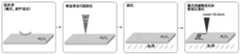
图1为实施例1中激光热解复合增材制造一体化前驱体陶瓷应变薄膜传感器的制作流程示意图。FIG. 1 is a schematic diagram of the manufacturing process of the integrated precursor ceramic strain thin film sensor of laser pyrolysis composite additive manufacturing in Example 1.
图2为实施例2中激光热解复合增材制造一体化前驱体陶瓷应变薄膜传感器的制作流程示意图。FIG. 2 is a schematic diagram of the manufacturing process of the integrated precursor ceramic strain thin film sensor of laser pyrolysis composite additive manufacturing in Example 2. FIG.
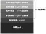
图3为实施例2中复合绝缘层的膜层结构示意图。FIG. 3 is a schematic diagram of the film structure of the composite insulating layer in Example 2. FIG.
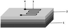
图4为实施例2中一体化薄膜应变传感器的结构图。FIG. 4 is a structural diagram of the integrated thin-film strain sensor in Example 2. FIG.
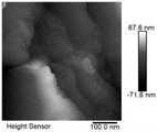
图5为敏感栅经过激光处理后的AFM图。Figure 5 is an AFM image of the sensitive grid after laser processing.
图6为实施例2中一体化薄膜应变传感器的应变信号测试图。FIG. 6 is a test diagram of the strain signal of the integrated thin film strain sensor in Example 2. FIG.
图中:1为镍基合金基底、2PDC复合绝缘膜层、3为PDC敏感栅、4敏感栅电极。In the figure: 1 is a nickel-based alloy substrate, 2 is a PDC composite insulating film layer, 3 is a PDC sensitive gate, and 4 is a sensitive gate electrode.
具体实施方式Detailed ways
为使本发明实施例的目的、技术方案和优点更加清楚,下面将结合本发明实施例,对本发明实施例中的技术方案进行清楚、完整地描述,显然,所描述的实施例是本发明一部分实施例,而不是全部的实施例。基于本发明中的实施例,本领域普通技术人员在没有作出创造性劳动前提下所获得的所有其他实施例,都属于本发明保护的范围。In order to make the purposes, technical solutions and advantages of the embodiments of the present invention clearer, the technical solutions in the embodiments of the present invention will be clearly and completely described below in conjunction with the embodiments of the present invention. Obviously, the described embodiments are part of the present invention. examples, but not all examples. Based on the embodiments of the present invention, all other embodiments obtained by those of ordinary skill in the art without creative efforts shall fall within the protection scope of the present invention.
实施例1Example 1
本实例中提供一种以激光热解复合增材制造前驱体陶瓷绝缘基应变传感器,由下而上依次为绝缘基底、应变敏感栅,敏感栅厚度介于10~20μm。This example provides a precursor ceramic insulating-based strain sensor manufactured by laser pyrolysis composite additive material. From bottom to top, there are an insulating substrate and a strain sensitive grid, and the thickness of the sensitive grid is between 10 and 20 μm.
上述激光诱导复合熔覆前驱体陶瓷绝缘基应变传感器的具体制备过程如图1所示,具体包括如下步骤:The specific preparation process of the above-mentioned laser-induced composite cladding precursor ceramic insulation-based strain sensor is shown in Figure 1, which specifically includes the following steps:
1)预处理:首先将氧化铝基底经过超声清洗20~60min,并在干燥箱中干燥后,取出。1) Pretreatment: First, the alumina substrate is ultrasonically cleaned for 20-60 minutes, dried in a drying box, and then taken out.
2)敏感栅的制备:配置导电粉末以及PDC的混合溶液,利用维森堡直写工艺,将其直写于步骤1)的绝缘基底上,经过固化20分钟后,进行激光处理,通过激光热解增强实现了有机物材料石墨化的转变,从AFM可以看出产生了石墨这种物质,如图5所示。2) Preparation of sensitive gate: configure a mixed solution of conductive powder and PDC, use the Wiesenberg direct writing process, and directly write it on the insulating substrate of step 1), after curing for 20 minutes, carry out laser treatment, and pass the laser heat. The solution enhancement realizes the transformation of the graphitization of organic materials, and it can be seen from the AFM that graphite is produced, as shown in Figure 5.
从而制备得所述的前驱体陶瓷绝缘基应变传感器。Thus, the precursor ceramic insulating-based strain sensor is prepared.
实施例2Example 2
本实例中提供一种激光热解复合增材制造一体化前驱体陶瓷应变薄膜传感器,由下而上依次为镍基合金基底、复合绝缘层、应变敏感栅,其中复合绝缘层厚度为50~200μm,敏感栅厚度介于10~20μm。In this example, a laser pyrolysis composite additive manufacturing integrated precursor ceramic strain thin film sensor is provided. From bottom to top, it is a nickel-based alloy substrate, a composite insulating layer, and a strain sensitive grid, wherein the thickness of the composite insulating layer is 50-200 μm. , the thickness of the sensitive gate is between 10 and 20 μm.
上述前驱体陶瓷一体化应变传感器的具体制备过程如图2所示,具体如下所述:The specific preparation process of the above-mentioned precursor-ceramic integrated strain sensor is shown in Figure 2, and the details are as follows:
1)预处理:将镍基合金片经过超声清洗20~60min,并在干燥箱中干燥后,通过磁控溅射机在镍基合金片上溅射沉积一层3~10μm的过渡层。1) Pretreatment: The nickel-based alloy sheet is ultrasonically cleaned for 20-60 minutes, and dried in a drying oven, and then a 3-10 μm transition layer is deposited on the nickel-based alloy sheet by a magnetron sputtering machine.
2)绝缘层的制备:配置PDC溶液、绝缘粉末与浸润作用的绝缘粉末混合溶液,在磁力搅拌台中搅拌1个小时后取出备用;利用维森堡直写工艺,精确控制绝缘层的大小,经过固化20~60min后,进行激光处理,等待其自然降至室温,利用丝网印刷技术在绝缘层上涂覆第二层同样的混合溶液,同样经过固化交联后经过相同的激光参数进行处理。2) Preparation of insulating layer: configure a mixed solution of PDC solution, insulating powder and insulating powder for infiltration, stir in a magnetic stirring table for 1 hour, and take it out for use; use the Wiesenberg direct writing process to precisely control the size of the insulating layer. After curing for 20-60 minutes, perform laser treatment, wait for it to naturally drop to room temperature, and use screen printing technology to coat the second layer of the same mixed solution on the insulating layer, which is also cured and cross-linked and then processed with the same laser parameters.
3)绝缘浸润层的制备:配置绝缘浸润粉末与PDC溶液的混合液,经过磁力搅拌1~2小时后取出,同样用丝网印刷涂覆混合液于步骤2)得到的绝缘层上,固化后经过激光扫描热处理,得到较为致密的浸润层,以同样的方法和参数制作第二层绝缘浸润层,最终得到如图3所示的复合绝缘膜层。3) Preparation of insulating infiltration layer: configure a mixture of insulating infiltration powder and PDC solution, take out after magnetic stirring for 1 to 2 hours, and also use screen printing to coat the mixture on the insulating layer obtained in step 2), and after curing After laser scanning heat treatment, a relatively dense wetting layer is obtained, and a second insulating wetting layer is fabricated with the same method and parameters, and finally a composite insulating film layer as shown in FIG. 3 is obtained.
4)敏感栅的制备:配置导电粉末以及PDC的混合溶液,利用维森堡直写工艺,将其直写于步骤2)和3)制备的复合绝缘层上,经过固化20分钟后,进行激光处理,通过激光热解增强了有机物到石墨化的转变,从AFM可以看出产生了石墨这种物质,如图5所示。4) Preparation of sensitive gate: configure the mixed solution of conductive powder and PDC, use the Wiisenberg direct writing process, write it directly on the composite insulating layer prepared in steps 2) and 3), and after curing for 20 minutes, laser light Treatment, the transformation of organics to graphitization was enhanced by laser pyrolysis, and it was seen from AFM that graphite was produced, as shown in Figure 5.
5)薄膜应变传感器的焊点和引线制作:通过商业化的石墨烯导电胶水将铂丝导线粘连在敏感栅的两个焊点上,静置5~12小时后,经过2小时120~150℃的加热处理,得到较为牢固的引线与焊点的接触。5) Fabrication of solder joints and leads of thin film strain sensor: The platinum wire is attached to the two solder joints of the sensitive grid by commercial graphene conductive glue, and after standing for 5 to 12 hours, after 2 hours at 120 to 150 ° C heat treatment to obtain a firmer contact between the lead and the solder joint.
从而制备得所述的前驱体陶瓷一体化薄膜应变传感器,如图4所示。Thus, the precursor-ceramic integrated thin-film strain sensor is prepared, as shown in FIG. 4 .
以上实施例仅用以说明本发明的技术方案,而非对其限制;尽管参照前述实施例对本发明进行了详细的说明,本领域的普通技术人员应当理解:其依然可以对前述各实施例所记载的技术方案进行修改,或者对其中部分技术特征进行等同替换;而这些修改或者替换,并不使相应技术方案的本质脱离本发明各实施例技术方案的精神和范围。The above embodiments are only used to illustrate the technical solutions of the present invention, but not to limit them; although the present invention has been described in detail with reference to the foregoing embodiments, those of ordinary skill in the art should understand that: The recorded technical solutions are modified, or some technical features thereof are equivalently replaced; and these modifications or replacements do not make the essence of the corresponding technical solutions deviate from the spirit and scope of the technical solutions of the embodiments of the present invention.
Claims (9)
Translated fromChinesePriority Applications (3)
| Application Number | Priority Date | Filing Date | Title |
|---|---|---|---|
| CN202111524535.5ACN114322741A (en) | 2021-12-14 | 2021-12-14 | Laser pyrolysis composite additive manufacturing integrated precursor ceramic thin film sensor and preparation method thereof |
| PCT/CN2022/136072WO2023109526A1 (en) | 2021-12-14 | 2022-12-02 | Integrated polymer-derived ceramic thin-film sensor prepared using combined laser pyrolysis and additive manufacturing, and preparation method therefor |
| US18/063,662US12371384B2 (en) | 2021-12-14 | 2022-12-08 | Integrated polymer-derived ceramic thin-film sensor produced by laser pyrolysis and additive manufacturing and fabrication method thereof |
Applications Claiming Priority (1)
| Application Number | Priority Date | Filing Date | Title |
|---|---|---|---|
| CN202111524535.5ACN114322741A (en) | 2021-12-14 | 2021-12-14 | Laser pyrolysis composite additive manufacturing integrated precursor ceramic thin film sensor and preparation method thereof |
Publications (1)
| Publication Number | Publication Date |
|---|---|
| CN114322741Atrue CN114322741A (en) | 2022-04-12 |
Family
ID=81050146
Family Applications (1)
| Application Number | Title | Priority Date | Filing Date |
|---|---|---|---|
| CN202111524535.5APendingCN114322741A (en) | 2021-12-14 | 2021-12-14 | Laser pyrolysis composite additive manufacturing integrated precursor ceramic thin film sensor and preparation method thereof |
Country Status (3)
| Country | Link |
|---|---|
| US (1) | US12371384B2 (en) |
| CN (1) | CN114322741A (en) |
| WO (1) | WO2023109526A1 (en) |
Cited By (5)
| Publication number | Priority date | Publication date | Assignee | Title |
|---|---|---|---|---|
| CN114974762A (en)* | 2022-05-26 | 2022-08-30 | 厦门大学 | High-temperature-resistant ceramic film thermistor with linear resistor-temperature relation |
| CN115112011A (en)* | 2022-06-20 | 2022-09-27 | 北京强度环境研究所 | A bonding process for surface-mounted resistance strain gauges of composite materials |
| CN115183932A (en)* | 2022-07-13 | 2022-10-14 | 哈尔滨工业大学(深圳) | Film type pressure sensor and preparation method thereof |
| WO2023109526A1 (en)* | 2021-12-14 | 2023-06-22 | 厦门大学 | Integrated polymer-derived ceramic thin-film sensor prepared using combined laser pyrolysis and additive manufacturing, and preparation method therefor |
| WO2023213625A1 (en) | 2022-05-03 | 2023-11-09 | Tdk Electronics Ag | Additive manufacturing method involving modification of sublayers |
Families Citing this family (2)
| Publication number | Priority date | Publication date | Assignee | Title |
|---|---|---|---|---|
| CN117798369B (en)* | 2024-02-29 | 2024-05-07 | 中北大学 | Metal-based ceramic sensor and preparation method thereof |
| CN118439869A (en)* | 2024-04-29 | 2024-08-06 | 岭南师范学院 | A method for preparing a polymer precursor ceramic high temperature thin film sensor |
Citations (6)
| Publication number | Priority date | Publication date | Assignee | Title |
|---|---|---|---|---|
| EP1308705A1 (en)* | 2001-10-27 | 2003-05-07 | Robert Bosch Gmbh | Manufacturing procedure of a sensor element and use of such an element |
| CN101241963A (en)* | 2007-12-12 | 2008-08-13 | 厦门三安电子有限公司 | Thin film LED chip device based on composite low-resistance buffer structure and manufacturing method thereof |
| CN101593631A (en)* | 2009-06-29 | 2009-12-02 | 彩虹集团公司 | A kind of preparation method of dye sensitization solar cell module |
| CN101669224A (en)* | 2005-06-01 | 2010-03-10 | 造型逻辑有限公司 | Layer selective laser ablation patterning |
| JP2014192465A (en)* | 2013-03-28 | 2014-10-06 | Fujifilm Corp | Manufacturing method of electric circuit wiring board |
| CN110957294A (en)* | 2019-12-11 | 2020-04-03 | 厦门大学 | Connecting structure of thin film sensor and processing method thereof |
Family Cites Families (7)
| Publication number | Priority date | Publication date | Assignee | Title |
|---|---|---|---|---|
| EP1378489A1 (en)* | 2002-07-03 | 2004-01-07 | Eidgenössische Technische Hochschule Zürich | Metal oxides prepared by flame spray pyrolysis |
| JP2006226860A (en)* | 2005-02-18 | 2006-08-31 | Hitachi Ltd | Ceramic sensor and manufacturing method thereof |
| CN101593831A (en) | 2009-06-29 | 2009-12-02 | 南开大学 | Sol-gel preparation method of lithium iron phosphate cathode material based on iron phosphate |
| JP2012193047A (en)* | 2011-03-14 | 2012-10-11 | Tdk Corp | Method for producing ceramic precursor thin film, and precursor solution |
| CN110518256A (en)* | 2019-08-06 | 2019-11-29 | 大连理工大学 | A method of it is composite porous using laser pyrolysis rapid, high volume manufacture high-test metal/carbon |
| CN110954234A (en)* | 2019-12-18 | 2020-04-03 | 厦门大学 | Polymer precursor ceramic film RTD and preparation method thereof |
| CN114322741A (en)* | 2021-12-14 | 2022-04-12 | 厦门大学 | Laser pyrolysis composite additive manufacturing integrated precursor ceramic thin film sensor and preparation method thereof |
- 2021
- 2021-12-14CNCN202111524535.5Apatent/CN114322741A/enactivePending
- 2022
- 2022-12-02WOPCT/CN2022/136072patent/WO2023109526A1/ennot_activeCeased
- 2022-12-08USUS18/063,662patent/US12371384B2/enactiveActive
Patent Citations (6)
| Publication number | Priority date | Publication date | Assignee | Title |
|---|---|---|---|---|
| EP1308705A1 (en)* | 2001-10-27 | 2003-05-07 | Robert Bosch Gmbh | Manufacturing procedure of a sensor element and use of such an element |
| CN101669224A (en)* | 2005-06-01 | 2010-03-10 | 造型逻辑有限公司 | Layer selective laser ablation patterning |
| CN101241963A (en)* | 2007-12-12 | 2008-08-13 | 厦门三安电子有限公司 | Thin film LED chip device based on composite low-resistance buffer structure and manufacturing method thereof |
| CN101593631A (en)* | 2009-06-29 | 2009-12-02 | 彩虹集团公司 | A kind of preparation method of dye sensitization solar cell module |
| JP2014192465A (en)* | 2013-03-28 | 2014-10-06 | Fujifilm Corp | Manufacturing method of electric circuit wiring board |
| CN110957294A (en)* | 2019-12-11 | 2020-04-03 | 厦门大学 | Connecting structure of thin film sensor and processing method thereof |
Non-Patent Citations (3)
| Title |
|---|
| 周颖锋 等: "航空发动机高温薄膜热电偶研究概况", 《航空制造技术》* |
| 李雅莉 等: "SiBCN高温薄膜温度传感器", 《微纳电子技术》* |
| 王广厚 等: "《团簇物理学》", 30 November 2003, 上海科学技术出版社* |
Cited By (6)
| Publication number | Priority date | Publication date | Assignee | Title |
|---|---|---|---|---|
| WO2023109526A1 (en)* | 2021-12-14 | 2023-06-22 | 厦门大学 | Integrated polymer-derived ceramic thin-film sensor prepared using combined laser pyrolysis and additive manufacturing, and preparation method therefor |
| WO2023213625A1 (en) | 2022-05-03 | 2023-11-09 | Tdk Electronics Ag | Additive manufacturing method involving modification of sublayers |
| DE102022110873A1 (en) | 2022-05-03 | 2023-11-09 | Tdk Electronics Ag | Additive manufacturing process with modification of partial layers |
| CN114974762A (en)* | 2022-05-26 | 2022-08-30 | 厦门大学 | High-temperature-resistant ceramic film thermistor with linear resistor-temperature relation |
| CN115112011A (en)* | 2022-06-20 | 2022-09-27 | 北京强度环境研究所 | A bonding process for surface-mounted resistance strain gauges of composite materials |
| CN115183932A (en)* | 2022-07-13 | 2022-10-14 | 哈尔滨工业大学(深圳) | Film type pressure sensor and preparation method thereof |
Also Published As
| Publication number | Publication date |
|---|---|
| US20230183138A1 (en) | 2023-06-15 |
| US12371384B2 (en) | 2025-07-29 |
| WO2023109526A1 (en) | 2023-06-22 |
Similar Documents
| Publication | Publication Date | Title |
|---|---|---|
| CN114322741A (en) | Laser pyrolysis composite additive manufacturing integrated precursor ceramic thin film sensor and preparation method thereof | |
| Li et al. | 3D printed high performance silver mesh for transparent glass heaters through liquid sacrificial substrate electric‐field‐driven jet | |
| TWI420540B (en) | Conductive material formed by light energy or thermal energy, preparation method of conductive material, and conductive composition | |
| CN108790368B (en) | Preparation method of graphene/metal composite material for high-speed train IGBT packaging | |
| WO2000027776A1 (en) | Carbon-based metal composite material, method for preparation thereof and use thereof | |
| CN105819882A (en) | Ceramic metal composite substrate and production method thereof | |
| CN116573953B (en) | Carbon/carbon composite material surface grid structure enhanced ablation-resistant coating, preparation method and application | |
| Li et al. | Multinozzle 3D printing of multilayer and thin flexible electronics | |
| CN110769527B (en) | Organic high-temperature electric heating composite film and preparation method thereof | |
| CN114910185A (en) | A high temperature thin film sensor of indium tin oxide based on laser pyrolysis combined with Wiesenberg direct writing | |
| CN108106748A (en) | A kind of flexibility ablation resistance film and preparation method thereof | |
| Dong et al. | Bioinspired High‐Adhesion Metallic Networks as Flexible Transparent Conductors | |
| CN113764137A (en) | Preparation method of nano silver wire conductive film, nano silver wire conductive film and application thereof | |
| Yang et al. | Ultra‐Thick Graphene Films with High Thermal Conductivity Through a Non‐Stacking Strategy | |
| JP2010098035A (en) | Thermoelectric conversion element | |
| CN110642644B (en) | Aluminum nitride ceramic copper-clad plate and preparation method thereof | |
| CN116001377B (en) | A high thermal conductivity graphene thermal control film with a weldable layer and a preparation method thereof | |
| CN118146010A (en) | Method for preparing oxide layered ceramic at low temperature | |
| CN114908322B (en) | Ablation-resistant three-dimensional inlaid ceramic coating and preparation method thereof | |
| CN202949681U (en) | Stacking structure of flexible graphite paper material and flexible graphite paper obtained through heat treatment | |
| CN105859302A (en) | Preparation method of ceramic material capable of generating carbon nanowires in situ | |
| CN101514277B (en) | High temperature resistance adhesive with low-expansion coefficients | |
| CN118510088B (en) | Far infrared heating plate and preparation method thereof | |
| CN119186970B (en) | Manufacturing method of high molecular weight modified siliconized polyurethane electrostatic chuck | |
| CN111780653B (en) | Carbon film nano conductive material-based resistor and preparation method thereof |
Legal Events
| Date | Code | Title | Description |
|---|---|---|---|
| PB01 | Publication | ||
| PB01 | Publication | ||
| SE01 | Entry into force of request for substantive examination | ||
| SE01 | Entry into force of request for substantive examination |