CN114315361A - Nanocrystalline silicon carbide superhard bulk material and preparation method thereof - Google Patents
Nanocrystalline silicon carbide superhard bulk material and preparation method thereofDownload PDFInfo
- Publication number
- CN114315361A CN114315361ACN202111574952.0ACN202111574952ACN114315361ACN 114315361 ACN114315361 ACN 114315361ACN 202111574952 ACN202111574952 ACN 202111574952ACN 114315361 ACN114315361 ACN 114315361A
- Authority
- CN
- China
- Prior art keywords
- silicon carbide
- sintering
- nanocrystalline silicon
- pressure
- nanocrystalline
- Prior art date
- Legal status (The legal status is an assumption and is not a legal conclusion. Google has not performed a legal analysis and makes no representation as to the accuracy of the status listed.)
- Granted
Links
Images


Classifications
- C—CHEMISTRY; METALLURGY
- C04—CEMENTS; CONCRETE; ARTIFICIAL STONE; CERAMICS; REFRACTORIES
- C04B—LIME, MAGNESIA; SLAG; CEMENTS; COMPOSITIONS THEREOF, e.g. MORTARS, CONCRETE OR LIKE BUILDING MATERIALS; ARTIFICIAL STONE; CERAMICS; REFRACTORIES; TREATMENT OF NATURAL STONE
- C04B35/00—Shaped ceramic products characterised by their composition; Ceramics compositions; Processing powders of inorganic compounds preparatory to the manufacturing of ceramic products
- C04B35/515—Shaped ceramic products characterised by their composition; Ceramics compositions; Processing powders of inorganic compounds preparatory to the manufacturing of ceramic products based on non-oxide ceramics
- C04B35/56—Shaped ceramic products characterised by their composition; Ceramics compositions; Processing powders of inorganic compounds preparatory to the manufacturing of ceramic products based on non-oxide ceramics based on carbides or oxycarbides
- C04B35/565—Shaped ceramic products characterised by their composition; Ceramics compositions; Processing powders of inorganic compounds preparatory to the manufacturing of ceramic products based on non-oxide ceramics based on carbides or oxycarbides based on silicon carbide
- C—CHEMISTRY; METALLURGY
- C04—CEMENTS; CONCRETE; ARTIFICIAL STONE; CERAMICS; REFRACTORIES
- C04B—LIME, MAGNESIA; SLAG; CEMENTS; COMPOSITIONS THEREOF, e.g. MORTARS, CONCRETE OR LIKE BUILDING MATERIALS; ARTIFICIAL STONE; CERAMICS; REFRACTORIES; TREATMENT OF NATURAL STONE
- C04B35/00—Shaped ceramic products characterised by their composition; Ceramics compositions; Processing powders of inorganic compounds preparatory to the manufacturing of ceramic products
- C04B35/622—Forming processes; Processing powders of inorganic compounds preparatory to the manufacturing of ceramic products
- C04B35/64—Burning or sintering processes
- C04B35/645—Pressure sintering
- C—CHEMISTRY; METALLURGY
- C04—CEMENTS; CONCRETE; ARTIFICIAL STONE; CERAMICS; REFRACTORIES
- C04B—LIME, MAGNESIA; SLAG; CEMENTS; COMPOSITIONS THEREOF, e.g. MORTARS, CONCRETE OR LIKE BUILDING MATERIALS; ARTIFICIAL STONE; CERAMICS; REFRACTORIES; TREATMENT OF NATURAL STONE
- C04B2235/00—Aspects relating to ceramic starting mixtures or sintered ceramic products
- C04B2235/70—Aspects relating to sintered or melt-casted ceramic products
- C04B2235/74—Physical characteristics
- C04B2235/78—Grain sizes and shapes, product microstructures, e.g. acicular grains, equiaxed grains, platelet-structures
- C—CHEMISTRY; METALLURGY
- C04—CEMENTS; CONCRETE; ARTIFICIAL STONE; CERAMICS; REFRACTORIES
- C04B—LIME, MAGNESIA; SLAG; CEMENTS; COMPOSITIONS THEREOF, e.g. MORTARS, CONCRETE OR LIKE BUILDING MATERIALS; ARTIFICIAL STONE; CERAMICS; REFRACTORIES; TREATMENT OF NATURAL STONE
- C04B2235/00—Aspects relating to ceramic starting mixtures or sintered ceramic products
- C04B2235/70—Aspects relating to sintered or melt-casted ceramic products
- C04B2235/96—Properties of ceramic products, e.g. mechanical properties such as strength, toughness, wear resistance
Landscapes
- Engineering & Computer Science (AREA)
- Chemical & Material Sciences (AREA)
- Ceramic Engineering (AREA)
- Manufacturing & Machinery (AREA)
- Materials Engineering (AREA)
- Structural Engineering (AREA)
- Organic Chemistry (AREA)
- Inorganic Chemistry (AREA)
- Ceramic Products (AREA)
- Carbon And Carbon Compounds (AREA)
Abstract
Translated fromChinese
Description
Translated fromChinese技术领域technical field
本申请属于无机非金属材料领域,具体涉及一种纳米晶碳化硅超硬块材及其制备方法。The application belongs to the field of inorganic non-metallic materials, and in particular relates to a nanocrystalline silicon carbide superhard block material and a preparation method thereof.
背景技术Background technique
维氏硬度超过40GPa的材料被称为超硬材料。超硬材料被广泛应用于切割、车削、研磨等工业领域。上世纪50年代,人们就已经成功合成了金刚石和立方氮化硼,然而,到目前为止,超硬材料仍然局限于这两大家族。研究人员为获得除金刚石以及立方氮化硼之外的超硬材料,进行了不懈的努力,却鲜有回报。与此同时,结构纳米化的方法被广泛地应用于提升金刚石以及立方氮化硼材料的硬度。例如,通过降低立方氮化硼的晶粒尺寸至14nm,其硬度可提升至85GPa,为单晶立方氮化硼硬度的两倍。然而,由于传统硬质材料块材难以烧结致密且同时减小晶粒尺寸的幅度有限,传统硬质材料一直没有实现超硬。Materials whose Vickers hardness exceeds 40GPa are called superhard materials. Superhard materials are widely used in cutting, turning, grinding and other industrial fields. In the 1950s, people have successfully synthesized diamond and cubic boron nitride, however, so far, superhard materials are still limited to these two families. Researchers have made unremitting efforts to obtain superhard materials other than diamond and cubic boron nitride, but have rarely paid off. At the same time, the method of structural nanostructure has been widely used to improve the hardness of diamond and cubic boron nitride materials. For example, by reducing the grain size of CBN to 14nm, its hardness can be increased to 85GPa, which is twice the hardness of single-crystal CBN. However, due to the difficulty of sintering and densifying the traditional hard material bulk and the limited range of grain size reduction at the same time, the traditional hard material has not achieved superhardness.
立方碳化硅作为一种常用的磨削和切割材料,在机械性能、化学以及热稳定性、制备工艺等方面具有很好的优势。然而作为一种传统的硬质材料,立方碳化硅的硬度在26GPa左右,限制了其在工业上的广泛应用。实验上,通过放电等离子体烧结以及热压烧结制备的纳米晶块材,虽具有较小的晶粒尺寸,但其致密性不好,存在不同程度的气孔。气孔的存在会对材料的机械性能产生不利的影响。此外,也有研究人员通过高温高压的方法,在4GPa,1500~1900℃条件下对碳化硅纳米粉进行烧结,虽然得到了致密的纳米晶碳化硅块材,但由于块材具有较大的晶粒尺寸,其维氏硬度未超过26GPa。As a commonly used grinding and cutting material, cubic silicon carbide has good advantages in mechanical properties, chemical and thermal stability, and preparation technology. However, as a traditional hard material, the hardness of cubic silicon carbide is around 26GPa, which limits its wide application in industry. Experimentally, although the nanocrystalline bulk material prepared by spark plasma sintering and hot pressing sintering has a small grain size, its compactness is not good, and there are different degrees of pores. The presence of pores can adversely affect the mechanical properties of the material. In addition, some researchers have sintered silicon carbide nanopowder at 4GPa and 1500-1900 ℃ by means of high temperature and high pressure. Although dense nanocrystalline silicon carbide bulk materials are obtained, the bulk materials have larger crystal grains. size, its Vickers hardness does not exceed 26GPa.
另外,中国专利申请CN104086179A公开了一种通过对硅粉和石墨粉进行球磨,然后进行烧结,得到碳化硅块体陶瓷的方法。该专利报道的块材密度是93.0~97.0%,硬度为31.4~42.4GPa,但并未公开其硬度测试方法。然而根据其他权威文献(例如,“MonolithicNanocrystalline SiC Ceramics”,Branko
发明内容SUMMARY OF THE INVENTION
鉴于上述现有技术中碳化硅陶瓷材料的种种不足,业界非常需要开发新型的具有超高硬度的碳化硅晶体材料。In view of various deficiencies of silicon carbide ceramic materials in the above-mentioned prior art, the industry needs to develop a new type of silicon carbide crystal material with ultra-high hardness.
本申请通过高温高压烧结经过预处理后的各种碳化硅原料,获得了超硬的纳米晶碳化硅块材。In the present application, superhard nanocrystalline silicon carbide bulk materials are obtained by sintering various pretreated silicon carbide raw materials at high temperature and high pressure.
因此,本申请的第一方面的技术方案是一种纳米晶碳化硅块材,其平均晶粒尺寸小于100nm,其维氏硬度等于或高于40GPa。Therefore, the technical solution of the first aspect of the present application is a nanocrystalline silicon carbide bulk material whose average grain size is less than 100 nm and whose Vickers hardness is equal to or higher than 40 GPa.
本申请的第二方面的技术方案是一种纳米晶碳化硅块材制备方法,该制备方法包括以下步骤:The technical solution of the second aspect of the present application is a method for preparing a nanocrystalline silicon carbide bulk material, and the preparation method includes the following steps:
A)预处理:称取一定质量的碳化硅纳米粉,进行酸洗处理,然后用水稀释至接近中性后取出,烘干;A) Pretreatment: weigh a certain quality of silicon carbide nano-powder, carry out pickling treatment, then dilute with water to near neutrality, take out, and dry;
B)预压成型:将烘干后的原料进行预压,得到预压坯体。B) Pre-press molding: pre-press the dried raw material to obtain a pre-pressed body.
C)烧结:对步骤B)得到的预压坯体进行高温高压烧结,其中烧结压力为4~28GPa,烧结温度为1000~2500℃,保温时间为1~60min。C) Sintering: perform high temperature and high pressure sintering on the pre-pressed body obtained in step B), wherein the sintering pressure is 4-28GPa, the sintering temperature is 1000-2500°C, and the holding time is 1-60min.
D)出料:对步骤C)中的高温高压烧结设备进行降温卸压,取出烧结后的碳化硅块体,进行任选的后处理。D) discharging: the high temperature and high pressure sintering equipment in step C) is cooled and pressure relieved, the sintered silicon carbide block is taken out, and optional post-processing is performed.
本发明与现有技术相比具有以下优点:Compared with the prior art, the present invention has the following advantages:
1.与没有进行预处理的烧结技术相比,本发明提出的预处理技术能有效地去除碳化硅纳米颗粒表面的二氧化硅层,从而提高碳化硅的活性,降低其致密烧结所需要的烧结条件(压力、温度等)。1. Compared with the sintering technology without pretreatment, the pretreatment technology proposed in the present invention can effectively remove the silicon dioxide layer on the surface of silicon carbide nanoparticles, thereby improving the activity of silicon carbide and reducing the sintering required for dense sintering. conditions (pressure, temperature, etc.).
2.区别于各种无压热压以及放电等离子烧结技术,高温高压技术所需要的烧结温度较低且不需要用任何助烧剂,碳化硅块材的晶界烧结良好,样品接近于透明。2. Different from various pressureless hot pressing and spark plasma sintering technologies, high temperature and high pressure technology requires lower sintering temperature and does not require any sintering aids.
3.区别于化学气相沉积得到的超硬碳化硅薄膜,高温高压烧结所获得的碳化硅为块材,厚度更厚,更适用于机械加工。此外,样品的尺寸可以进一步做大,实际的应用范围更加的广阔。3. Different from the superhard silicon carbide film obtained by chemical vapor deposition, the silicon carbide obtained by high temperature and high pressure sintering is a bulk material with thicker thickness and is more suitable for machining. In addition, the size of the sample can be further enlarged, and the practical application range is wider.
4.在高温高压烧结中,高温可以促进晶粒间的合并以及强界面的生成,高压可以束缚原子扩散,限制晶粒粗化,从而提高了烧结样品的致密度和硬度。所得碳化硅样品平均晶粒尺寸很小,最小可达10nm以下。且通过调节原料前驱体和烧结工艺,可以得到各种晶粒尺寸的纳米晶超硬碳化硅块材。4. In high temperature and high pressure sintering, high temperature can promote the coalescence between grains and the formation of strong interfaces, and high pressure can restrain atomic diffusion and limit grain coarsening, thereby improving the density and hardness of sintered samples. The average grain size of the obtained silicon carbide samples is very small, and the smallest can be less than 10 nm. And by adjusting the raw material precursor and the sintering process, nanocrystalline superhard silicon carbide bulk materials with various grain sizes can be obtained.
5.所得碳化硅样品维氏硬度的真实测量值等于或高于40GPa,是一种新的超硬材料,丰富了超硬材料家族。这种材料可制成刀具,在精密加工领域具有很大的应用潜力。因此,这一研究结果对扩大碳化硅的应用范围以及指导合成新的超硬材料具有重要的意义。5. The real measured value of Vickers hardness of the obtained silicon carbide sample is equal to or higher than 40GPa, which is a new superhard material and enriches the superhard material family. This material can be made into tools and has great application potential in the field of precision machining. Therefore, this research result is of great significance for expanding the application range of SiC and guiding the synthesis of new superhard materials.
下面结合附图和具体实施方式对本申请的纳米晶碳化硅块材及其制备方法做进一步的详细描述。The nanocrystalline silicon carbide bulk material and its preparation method of the present application will be further described in detail below with reference to the accompanying drawings and specific embodiments.
附图说明Description of drawings
图1中(A)、(B)、(C)、(D)、(E)分别示出了本申请实施例1、2、3、4、5所得样品的光学照片;(A), (B), (C), (D), (E) in Figure 1 show the optical photos of the samples obtained in Examples 1, 2, 3, 4, and 5 of the present application, respectively;
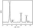
图2示出了本申请实施例4得到纳米晶碳化硅超硬块材的X射线衍射图;2 shows the X-ray diffraction pattern of the nanocrystalline silicon carbide superhard bulk material obtained in Example 4 of the present application;
图3示出了本申请实施例4得到纳米晶碳化硅超硬块材的断口扫描电镜图片;Fig. 3 shows the fracture scanning electron microscope picture of the nanocrystalline silicon carbide superhard block obtained in Example 4 of the present application;
图4示出了本申请实施例4得到纳米晶碳化硅超硬块材的透射电镜图片,(A)是样品的低倍透射电镜图片,(B)是样品中某一晶粒的高角环形暗场像,(C)是样品的选区电子衍射图;Figure 4 shows the transmission electron microscope picture of the nanocrystalline silicon carbide superhard bulk material obtained in Example 4 of the present application, (A) is the low magnification transmission electron microscope picture of the sample, (B) is the high-angle annular dark field of a certain grain in the sample image, (C) is the selected area electron diffraction pattern of the sample;
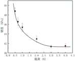
图5示出了本申请实施例4得到纳米晶碳化硅超硬块材的硬度-载荷曲线。FIG. 5 shows the hardness-load curve of the nanocrystalline silicon carbide superhard bulk material obtained in Example 4 of the present application.
具体实施方式Detailed ways
本申请的第一方面的技术方案是一种纳米晶碳化硅块材,其平均晶粒尺寸小于100nm,其维氏硬度等于或高于40GPa。The technical solution of the first aspect of the present application is a nanocrystalline silicon carbide bulk material whose average grain size is less than 100 nm and whose Vickers hardness is equal to or higher than 40 GPa.
在本申请中,除非另有指明或定义,所有的术语应被解释为具有按照本领域技术人员所通常理解的含义。In this application, unless otherwise indicated or defined, all terms should be construed as having the meaning as commonly understood by those skilled in the art.
在本申请的上下文中,“纳米晶碳化硅”是指从化学组成上看,基本由纯碳化硅构成的材料,而且从微观结构上看,材料由众多的尺寸在纳米级的碳化硅晶粒构成。In the context of this application, "nanocrystalline silicon carbide" refers to a material that, from a chemical composition point of view, consists essentially of pure silicon carbide, and from a microstructural point of view, the material consists of numerous silicon carbide grains with a size in the nanometer scale. constitute.
在本申请的上下文中,“维氏硬度”是指通过压痕法测量得到的材料硬度,即通过施加一定载荷使压头(通常为金刚石压头)压入被测试样品,在卸去载荷后在样品表面留下塑性变形的痕迹,然后将施加的载荷除以压痕的面积就得到样品的维氏硬度。维氏硬度测量时使用相对面间夹角为136°的金刚石正棱锥体压头在一定压力的作用下,垂直压入材料表面并保持一定时间,在样品表面留下塑性变形产生的菱形压痕;根据测量卸载后留下的压痕对角线长度,从而算出压痕的面积。具体地,维氏硬度的计算公式是:Hv=1854.4F/L2,其中F为加载的载荷大小,单位为N;L为压痕平均对角线长度,单位为μm。值得注意的是,由于材料的硬度值在一定压力载荷范围内是变化的,尤其对于超硬材料来说,材料的刚度较高,小载荷作用下压坑的弹性应变较大,导致其硬度测量值偏高,只有当载荷大于某个极限值时,材料硬度才趋于一个恒定数值,即渐进线硬度值。对于本申请的纳米晶碳化硅块材而言,所有维氏硬度均是以变载荷测量方式获得的材料的真实硬度值,即采用变载荷方式测量材料的硬度,取硬度-载荷曲线中硬度值随载荷不变区域的硬度值(即渐进线硬度值)作为最终测量值。In the context of this application, "Vickers hardness" refers to the hardness of a material measured by the indentation method, i.e. by applying a certain load to press an indenter (usually a diamond indenter) into the sample to be tested, after the load is removed A trace of plastic deformation is left on the surface of the sample, and the Vickers hardness of the sample is obtained by dividing the applied load by the area of the indentation. In Vickers hardness measurement, a diamond regular pyramid indenter with an included angle of 136° between the opposite surfaces is used to vertically press into the material surface and hold for a certain period of time under the action of a certain pressure, leaving a diamond-shaped indentation produced by plastic deformation on the surface of the sample. ; Calculate the area of the indentation by measuring the diagonal length of the indentation left after unloading. Specifically, the calculation formula of Vickers hardness is: Hv =1854.4F/L2 , where F is the applied load, the unit is N; L is the average diagonal length of the indentation, the unit is μm. It is worth noting that since the hardness value of the material varies within a certain pressure load range, especially for superhard materials, the stiffness of the material is high, and the elastic strain of the indentation under a small load is large, which leads to its hardness measurement. If the value is too high, only when the load is greater than a certain limit value, the material hardness tends to a constant value, that is, the asymptotic hardness value. For the nanocrystalline silicon carbide bulk material of the present application, all Vickers hardnesses are the real hardness values of the material obtained by the variable load measurement method, that is, the hardness of the material is measured by the variable load method, and the hardness value in the hardness-load curve is taken. The hardness value in the region that does not change with the load (ie, the asymptotic hardness value) is used as the final measurement value.
本领域技术人员了解有多种技术手段可以获取材料的微观结构信息;例如,可以利用扫描电镜或透射电镜等仪器进行直接观察,或利用X射线谱图进行分析。为了准确表征,优选对材料内部样品进行分析;另外,为了避免样品中可能存在的少量污染物的干扰,可以随机取多个(例如3个以上或5个以上)样品点进行分析。Those skilled in the art understand that there are various technical means to obtain the microstructural information of the material; for example, direct observation can be carried out with instruments such as scanning electron microscope or transmission electron microscope, or X-ray spectrum can be used for analysis. For accurate characterization, it is preferable to analyze the internal sample of the material; in addition, in order to avoid the interference of a small amount of contaminants that may exist in the sample, multiple (for example, more than 3 or more than 5) sample points can be randomly selected for analysis.
本领域技术人员可以理解,本申请的纳米晶碳化硅块材基本上由纯碳化硅构成,但并不排除原料本身中存在的或加工制造过程中无意引入的不可避免的少量杂质。就本申请目的而言,本申请的纳米晶碳化硅材料中杂质的重量含量通常最多5%,优选少于4%,更优选少于3%,例如少于2%、少于1%、少于0.5%。Those skilled in the art can understand that the nanocrystalline silicon carbide bulk material of the present application is basically composed of pure silicon carbide, but it does not exclude a small amount of unavoidable impurities that exist in the raw material itself or are unintentionally introduced in the manufacturing process. For the purpose of the present application, the weight content of impurities in the nanocrystalline silicon carbide material of the present application is usually at most 5%, preferably less than 4%, more preferably less than 3%, such as less than 2%, less than 1%, less than at 0.5%.
本申请的纳米晶碳化硅块材中碳化硅晶粒的晶粒尺寸一般在1nm~100nm之间,例如所述晶粒尺寸可以大于2nm、大于3nm、大于4nm、大于5nm、大于8nm、大于10nm、大于20nm、大于30nm、大于40nm、大于50nm,所述晶粒尺寸可以小于100nm、小于90nm、小于80nm、小于70nm、小于60nm、小于50nm。碳化硅的晶粒尺寸可以由本领域技术人员根据XRD数据结合谢乐公式计算得到。The grain size of the silicon carbide grains in the nanocrystalline silicon carbide bulk material of the present application is generally between 1 nm and 100 nm, for example, the grain size may be greater than 2 nm, greater than 3 nm, greater than 4 nm, greater than 5 nm, greater than 8 nm, greater than 10 nm , greater than 20 nm, greater than 30 nm, greater than 40 nm, greater than 50 nm, the grain size can be less than 100 nm, less than 90 nm, less than 80 nm, less than 70 nm, less than 60 nm, less than 50 nm. The grain size of silicon carbide can be calculated by those skilled in the art based on XRD data combined with Scherrer's formula.
本申请的纳米晶碳化硅是块材,即以块体材料形式使用。“块材”在本申请中被理解为独立存在的单个材料体,其三个维度的尺寸之间不存在巨大差异,从而有别于纤维状材料、薄片或薄膜状材料、以及粉末或颗粒状材料。本申请的纳米晶碳化硅是块材的,其体积通常至少为0.05mm3,例如至少0.1mm3、至少0.5mm3、至少1mm3、至少5mm3、至少10mm3、至少20mm3、至少50mm3、至少100mm3等块体材料的体积上限并不受特别限制,可以根据实际需要和设备加工能力酌情选择,例如可以高达1000cm3。The nanocrystalline silicon carbide of the present application is a bulk material, that is, it is used in the form of a bulk material. A "bulk" is understood in this application as a single body of material that exists independently, the dimensions of which do not differ greatly in its three dimensions, thus distinguishing it from fibrous, flake or film-like materials, and powders or granules Material. The nanocrystalline silicon carbide of the present application is bulk, typically at least0.05mm3 in volume, such as at least0.1mm3 , at least0.5mm3 , at least1mm3 , at least5mm3 , at least10mm3 , at least20mm3 , at least 50mm3. The upper limit of the volume of bulk materials such as at least 100 mm3 is not particularly limited, and can be selected according to actual needs and equipment processing capacity, for example, it can be as high as 1000 cm3 .
本申请对纳米晶碳化硅块材的形状并无特别限制,根据实际需要,可以采用相应的模具直接制成或经切削研磨而加工成各种形状的块材,例如圆柱形、棱柱形、球形等等。例如,纳米晶碳化硅块材可以是直径为0.5~80mm,高度为0.5~50mm的圆柱形。The shape of the nanocrystalline silicon carbide block is not particularly limited in this application. According to actual needs, it can be directly made by corresponding molds or processed into blocks of various shapes by cutting and grinding, such as cylindrical, prismatic, spherical and many more. For example, the bulk nanocrystalline silicon carbide may be cylindrical with a diameter of 0.5-80 mm and a height of 0.5-50 mm.
本申请的纳米晶碳化硅块材具有高硬度,其维氏硬度一般大于或等于40GPa,例如大于40.5GPa、大于41.5GPa、大于42GPa、大于42.5GPa、大于43GPa、大于44GPa、或甚至大于45GPa。The nanocrystalline silicon carbide bulk material of the present application has high hardness, and its Vickers hardness is generally greater than or equal to 40GPa, such as greater than 40.5GPa, greater than 41.5GPa, greater than 42GPa, greater than 42.5GPa, greater than 43GPa, greater than 44GPa, or even greater than 45GPa.
本申请的第二方面提供了一种制备第一方面所述纳米晶碳化硅块材的方法,该方法包括如下步骤:A second aspect of the present application provides a method for preparing the bulk nanocrystalline silicon carbide material of the first aspect, the method comprising the steps of:
A)预处理:称取一定质量的碳化硅纳米粉,进行酸洗处理,然后用水稀释至接近中性后取出,烘干;A) Pretreatment: weigh a certain quality of silicon carbide nano-powder, carry out pickling treatment, then dilute with water to near neutrality, take out, and dry;
B)预压成型:将烘干后的原料进行预压,得到预压坯体;B) pre-press molding: pre-press the dried raw material to obtain a pre-pressed body;
C)烧结:对步骤B)得到的预压坯体进行高温高压烧结,其中烧结压力为4~28GPa,烧结温度为1000~2500℃,保温时间为1~60min;C) Sintering: perform high temperature and high pressure sintering on the pre-pressed body obtained in step B), wherein the sintering pressure is 4-28GPa, the sintering temperature is 1000-2500°C, and the holding time is 1-60min;
D)出料:对步骤C)中的高温高压烧结设备进行降温卸压,取出烧结后的碳化硅块体,进行任选的后处理。D) discharging: the high temperature and high pressure sintering equipment in step C) is cooled and pressure relieved, the sintered silicon carbide block is taken out, and optional post-processing is performed.
方法的步骤A)中所用碳原料为碳化硅纳米粉,即晶粒尺寸为纳米级的碳化硅粉末。优选地,所用的碳化硅纳米粉的晶粒尺寸为5~100nm(例如6nm、8nm、10nm、12nm、15nm、20nm、30nm、40nm、50nm、60nm、70nm、80nm、90nm或以这些尺寸为端点构成的任意数值范围内的任意晶粒尺寸),优选为5~50nm。方法中可以采用单一晶粒尺寸的碳化硅纳米粉或是采用几种不同晶粒尺寸的碳化硅纳米粉的混合物。粉末的晶粒尺寸可以根据XRD数据通过本领域众所周知的谢乐公式进行估算。The carbon raw material used in step A) of the method is silicon carbide nanopowder, that is, silicon carbide powder with nanometer grain size. Preferably, the grain size of the silicon carbide nanopowder used is 5-100 nm (for example, 6 nm, 8 nm, 10 nm, 12 nm, 15 nm, 20 nm, 30 nm, 40 nm, 50 nm, 60 nm, 70 nm, 80 nm, 90 nm, or with these sizes as the endpoints. Any crystal grain size within an arbitrary numerical range of the composition), preferably 5 to 50 nm. In the method, a single grain size silicon carbide nanopowder or a mixture of several silicon carbide nanopowders with different grain sizes can be used. The grain size of the powder can be estimated from the XRD data by the Scherrer formula well known in the art.
方法的步骤A)中所用的各种原料优选地是高纯度的,例如其纯度优选高于97%,更优选高于98%、高于99%或高于99.5%。The various starting materials used in step A) of the process are preferably of high purity, eg preferably above 97% pure, more preferably above 98%, above 99% or above 99.5% pure.
方法的步骤A)中酸洗所用的酸优选为氢氟酸,其浓度优选为10%~40%,酸洗时间通常为15~90min。The acid used for pickling in step A) of the method is preferably hydrofluoric acid, and its concentration is preferably 10% to 40%, and the pickling time is usually 15 to 90 minutes.
方法的步骤A)中所用的水优选为去离子水。可以用水将酸洗液稀释至接近中性(约pH7),即约pH 6~8,更优选pH 6.5~7.5。The water used in step A) of the process is preferably deionized water. The acid wash can be diluted with water to near neutral (about pH 7), ie about pH 6-8, more preferably pH 6.5-7.5.
方法的步骤A)中的酸洗优选在聚四氟乙烯容器中、在超声波作用下进行。例如,可以将碳化硅纳米粉和酸放置于聚四氟乙烯瓶中,而聚四氟乙烯瓶置于超声波清洗机里。超声处理过程例如可以以工作10min、静置5min为一个循环(一个循环时长记15min),可以进行多个循环,超声的总时长与酸洗时间可以相同或不同。超声波处理可以保证原料在酸中充分分散。The pickling in step A) of the method is preferably carried out in a polytetrafluoroethylene vessel under the action of ultrasound. For example, silicon carbide nanopowder and acid can be placed in a teflon bottle, and the teflon bottle can be placed in an ultrasonic cleaner. For example, in the ultrasonic treatment process, a cycle of 10 minutes of work and 5 minutes of standing can be used as one cycle (the duration of one cycle is recorded as 15 minutes), and multiple cycles can be performed. The total duration of ultrasonication and the pickling time can be the same or different. Ultrasonic treatment can ensure that the raw materials are fully dispersed in the acid.
在一些优选的实施方式中,方法的步骤A)中的酸洗过程中同时使用离心机和超声清洗机。离心处理会加速原料沉降,使之与酸液分离,例如设置转速为4000~11000r/min,离心时间为10~20min;而超声处理使沉降的原料与新加入的去离子水混合均匀,超声时间为5~10min。重复几次直至pH接近于7。In some preferred embodiments, both a centrifuge and an ultrasonic cleaner are used during the pickling process in step A) of the method. Centrifugal treatment will accelerate the sedimentation of raw materials and separate them from the acid solution. For example, set the rotating speed to 4000-11000r/min and the centrifugation time to 10-20min; while ultrasonic treatment makes the sedimented raw materials and newly added deionized water evenly mixed, and the
方法的步骤A)中的烘干可以在各种常规干燥设备中进行。优选地,步骤A)中的烘干操作使用真空干燥箱进行,其真空度设置高于1×10⁻¹Pa,烘干温度为40~80℃,烘干时间为12~24h。The drying in step A) of the method can be carried out in various conventional drying equipment. Preferably, the drying operation in step A) is performed using a vacuum drying oven, the vacuum degree of which is set to be higher than 1×10⁻¹ Pa, the drying temperature is 40-80° C., and the drying time is 12-24 h.
方法的步骤A)中的预处理能有效地去除碳化硅纳米颗粒表面的二氧化硅层,从而提高碳化硅的活性,降低其致密烧结所需要的烧结条件(压力、温度等),更有利于改善烧结样品的硬度和致密度。The pretreatment in step A) of the method can effectively remove the silicon dioxide layer on the surface of silicon carbide nanoparticles, thereby improving the activity of silicon carbide, reducing the sintering conditions (pressure, temperature, etc.) required for its dense sintering, which is more conducive to Improve the hardness and density of sintered samples.
在方法的步骤B)中对烘干后的原料进行预压,得到预压坯。所述坯体根据需要可以是任意形状,例如柱体、块体和球体等。预压成坯可以在常规压坯机或液压机上进行,通常在室温下操作即可,可以在空气中或惰性气氛中进行。本申请的方法的步骤二中的预压压力没有特别限制,只要保证坯体密实即可,但为了达到更好的效果,预压压力应达到5MPa以上,例如8MPa、10MPa、20MPa等,优选的预压压力为5~10MPa。预压保持时间优选为0.5min以上和10min以内,更优选为1~5min。In step B) of the method, the dried raw material is pre-pressed to obtain a pre-compact. The green body can be in any shape as required, such as a cylinder, a block, a sphere, and the like. Pre-compacting can be carried out on a conventional compacting machine or a hydraulic machine, usually at room temperature, and can be carried out in air or in an inert atmosphere. The pre-pressing pressure in step 2 of the method of the present application is not particularly limited, as long as the compact body is ensured, but in order to achieve a better effect, the pre-pressing pressure should reach more than 5 MPa, such as 8 MPa, 10 MPa, 20 MPa, etc., preferably The preload pressure is 5-10MPa. The preload holding time is preferably 0.5 min or more and 10 min or less, and more preferably 1 to 5 min.
在本申请的优选实施方式中,预压模式为双向加压。这样能够使成型模具内的粉料双向均匀受力,降低了预压坯上下压力梯度,避免预压坯上下密度相差较大,进而影响烧结后块体的整体致密度,从而使得坯体致密度更高,更有助于提高合成样品的性能。In a preferred embodiment of the present application, the pre-compression mode is bidirectional compression. In this way, the powder in the molding die can be uniformly stressed in both directions, which reduces the pressure gradient between the upper and lower preforms, and avoids a large difference in the upper and lower densities of the preforms. Higher, more helpful to improve the performance of synthetic samples.
在方法的步骤C)中对步骤B)得到的预压坯体进行高温高压烧结。在本申请的一个优选实施方式中,在4GPa以上28GPa以下的烧结压力、1000℃以上2500℃以下温度条件下进行烧结,保温时间为1~60min,以得到具有高硬度的碳化硅陶瓷。烧结压力例如为4GPa、5GPa、6GPa、7GPa、8GPa、9GPa、10GPa、11GPa、12GPa、13GPa、14GPa、15Pa、16GPa、17GPa、18GPa、19GPa、20GPa、21GPa、22GPa、23GPa、24GPa、25GPa、26GPa、27GPa、28GPa等或这些压力范围之内的任意压力。通常,更高的烧结压力有利于提高烧结样品硬度,因此烧结压力优选为10~28GPa。烧结温度例如可以为1000℃、1100℃、1200℃、1300℃、1400℃、1500℃、1600℃、1700℃、1800℃、1900℃、2000℃、2100℃、2200℃、2300℃、2400℃、2500℃等温度或这些温度范围之内的任意温度。在步骤C)中,优选保温时间为1~60min,例如5~45min或5~30min。步骤C)中升温速率可以控制在50~150℃/min之间。In step C) of the method, the pre-compact body obtained in step B) is sintered at high temperature and high pressure. In a preferred embodiment of the present application, sintering is performed at a sintering pressure of 4GPa or more and 28GPa or less, and a temperature of 1000°C or more and 2500°C or less, and the holding time is 1 to 60 minutes to obtain silicon carbide ceramics with high hardness. The sintering pressure is, for example, 4GPa, 5GPa, 6GPa, 7GPa, 8GPa, 9GPa, 10GPa, 11GPa, 12GPa, 13GPa, 14GPa, 15Pa, 16GPa, 17GPa, 18GPa, 19GPa, 20GPa, 21GPa, 22GPa, 23GPa, 24GPa, 25GPa, 26GPa, 27GPa, 28GPa, etc. or any pressure within these pressure ranges. Generally, a higher sintering pressure is beneficial to improve the hardness of the sintered sample, so the sintering pressure is preferably 10-28 GPa. The sintering temperature can be, for example, 1000°C, 1100°C, 1200°C, 1300°C, 1400°C, 1500°C, 1600°C, 1700°C, 1800°C, 1900°C, 2000°C, 2100°C, 2200°C, 2300°C, 2400°C, Temperatures such as 2500°C or any temperature within these temperature ranges. In step C), preferably the holding time is 1-60 min, for example, 5-45 min or 5-30 min. In step C), the heating rate can be controlled between 50 and 150° C./min.
烧结处理可以采用本领域技术人员熟知的高温高压烧结设备进行,例如美国Rockland Research公司生产的T25型压机或桂林冶金机械总厂制造的六面顶液压机CS-1B。烧结过程视需要可以在惰性气氛中进行,或在空气中进行。The sintering treatment can be carried out by using high temperature and high pressure sintering equipment well known to those skilled in the art, such as T25 type press produced by Rockland Research Company of the United States or CS-1B hydraulic press with six-sided roof produced by Guilin Metallurgical Machinery General Plant. The sintering process can be carried out in an inert atmosphere, or in air, if desired.
对于高温高压烧结,通常先将步骤B)得到的预压坯体装入坩埚(例如氮化硼坩埚)中,然后放入组装块中进行高温高压烧结。其中组装块包括加热体、保温层、传压层等,加热体为铼片和/或石墨,保温层为氧化锆和/或氧化铝,传压层为氧化镁和/或铬酸镧。For high temperature and high pressure sintering, the pre-compact body obtained in step B) is usually loaded into a crucible (such as a boron nitride crucible), and then placed into an assembly block for high temperature and high pressure sintering. The assembly block includes a heating body, a heat insulating layer, a pressure transfer layer, etc. The heating body is rhenium sheet and/or graphite, the heat insulating layer is zirconia and/or aluminum oxide, and the pressure transfer layer is magnesium oxide and/or lanthanum chromate.
烧结完成后,在步骤D)中对烧结样品进行冷却,使烧结样品及烧结设备的腔体降至室温,并且将设备内压调至环境压力(即卸压),然后取出烧结样品,进行任选的加工和后处理(例如研磨和抛光等)后,即得到本申请的纳米晶碳化硅超硬块材。步骤D)中的冷却可以自然冷却或进行受控冷却,例如降温速率可以为50~150℃/min。After the sintering is completed, the sintered sample is cooled in step D), so that the sintered sample and the cavity of the sintering device are lowered to room temperature, and the internal pressure of the device is adjusted to the ambient pressure (ie, pressure relief), and then the sintered sample is taken out, and any After selected processing and post-processing (such as grinding and polishing, etc.), the nanocrystalline silicon carbide superhard bulk material of the present application is obtained. The cooling in step D) can be natural cooling or controlled cooling, for example, the cooling rate can be 50-150°C/min.
本发明通过优化高温高压烧结条件,以碳化硅纳米粉为原料获得了纳米晶碳化硅超硬块材。块材的致密化以及晶粒的细化是制备具有更高硬度的纳米晶碳化硅所必需的前提。本发明通过调节原料尺寸、改进预处理工艺以及调整烧结参数(压力、温度、保温时间等),获得了具有良好的致密度以及更细小的晶粒纳米晶碳化硅,从而得到了超硬碳化硅陶瓷块材。高温高压烧结比放电等离子体烧结和热压烧结的烧结压力更高,更容易获得致密的纳米晶块材。The present invention obtains nanocrystalline silicon carbide superhard bulk material by optimizing high temperature and high pressure sintering conditions and using silicon carbide nano powder as raw material. The densification of the bulk material and the refinement of the grains are necessary prerequisites for the preparation of nanocrystalline silicon carbide with higher hardness. The invention obtains nanocrystalline silicon carbide with good density and finer grains by adjusting the size of raw materials, improving the pretreatment process and adjusting the sintering parameters (pressure, temperature, holding time, etc.), thereby obtaining superhard silicon carbide Ceramic blocks. High temperature and high pressure sintering has higher sintering pressure than spark plasma sintering and hot pressing sintering, and it is easier to obtain dense nanocrystalline bulk materials.
下面结合实施例对本申请的纳米晶碳化硅块材和制备方法做进一步描述。The nanocrystalline silicon carbide bulk material and the preparation method of the present application will be further described below with reference to the examples.
实施例Example
以下描述的实施例是本申请一部分实施例,而不是全部的实施例。本申请的实施例的详细描述并非旨在限制要求保护的本申请的范围,而是仅仅表示本申请的特定实施例。基于本申请中的实施例,本领域普通技术人员在不脱离本申请原理、没有做出创造性劳动前提下所获得的所有其他实施例,都属于本申请保护的范围。The embodiments described below are some, but not all, embodiments of the present application. The detailed descriptions of the embodiments of the application are not intended to limit the scope of the application as claimed, but are merely representative of specific embodiments of the application. Based on the embodiments in the present application, all other embodiments obtained by those of ordinary skill in the art without departing from the principles of the present application and without creative work, fall within the protection scope of the present application.
为了简明起见,一些本领域常规采用的材料、设备和方法步骤未在实施例中一一注明。凡是在实施例中未具体注明的工艺方法和分析测试过程(及相关参数)均按本领域技术人员通常所采用的进行;未注明具体来源的材料和设备均为实验室常规材料和设备。For the sake of brevity, some materials, equipment and method steps conventionally used in the art are not specified in the examples. All the technical methods and analysis and testing procedures (and related parameters) not specifically indicated in the examples are carried out by those skilled in the art; the materials and equipment that do not indicate specific sources are laboratory routine materials and equipment. .
设备和材料分析检测方法Equipment and material analysis and testing methods
各实施例中所用高温高压烧结装置为美国Rockland Research公司生产的T25型压机或或桂林冶金机械总厂制造的六面顶液压机CS-1B;各实施例中所用碳化硅粉末原料由Alfa Aesar提供。The high-temperature and high-pressure sintering device used in each example is a T25 press produced by Rockland Research Company in the United States or a six-sided top hydraulic press CS-1B produced by Guilin Metallurgical Machinery General Plant; the silicon carbide powder raw material used in each example is provided by Alfa Aesar .
各实施例中所用主要分析检测方法及所用仪器如下:The main analysis and detection methods used in each embodiment and the used instruments are as follows:
X射线衍射:采用Rigaku DMAX-2500/P进行XRD图谱的测定。扫描速度为0.1度每分钟,范围为20度~90度。X-ray diffraction: Rigaku DMAX-2500/P was used to measure the XRD pattern. The scanning speed is 0.1 degrees per minute, and the range is 20 degrees to 90 degrees.
粉体原料及块体的的晶粒尺寸:根据XRD数据结合谢乐公式,估算原料和块体的的晶粒尺寸。Grain size of powder raw material and bulk: According to XRD data combined with Scherrer formula, the grain size of raw material and bulk is estimated.
SEM:采用赛默飞Scios DualBeam进行样品断口分析。电压为5KV,电流为0.1nA。SEM: Fracture analysis of samples was performed using Thermo Scientific Scios DualBeam. The voltage is 5KV and the current is 0.1nA.
TEM以及HAADF:利用聚焦离子束(FIB)制备了TEM样品(5×10×0.08μm),采用赛默飞Talos F200X扫描透射电镜(美国赛默飞世尔科技公司)进行进行测试,加速电压为200kV。TEM and HAADF: TEM samples (5 × 10 × 0.08 μm) were prepared by focused ion beam (FIB), and tested by Thermo Fisher Talos F200X scanning transmission electron microscope (Thermo Fisher Scientific, USA), and the accelerating voltage was 200kV.
维氏硬度检测方法:采用德国KB-30-S型显微硬度仪对样品进行显微硬度的测试,测试参数为加载10s,保压15s。即使用相对面间夹角为136°的金刚石正棱锥体压头在一定压力的作用下,垂直压入材料表面并保持一定时间(加载10s,保压15s),在样品表面留下塑性变形产生的菱形压痕,然后将施加的载荷除以压痕的面积就是压痕法测量得到的硬度。维氏硬度的计算公式是:Hv=1854.4F/L2,其中F为加载的载荷大小,单位为N;L为压痕平均对角线长度,单位为μm。硬度测量采用变载荷方式进行,取样品硬度值取随载荷不变区域的测量值(即渐进线硬度值)作为最终的硬度测量值,如图5所示。Vickers hardness testing method: German KB-30-S microhardness tester was used to test the microhardness of the samples. The test parameters were loading for 10s and holding pressure for 15s. That is, using a diamond regular pyramid indenter with an angle of 136° between the opposite surfaces, under the action of a certain pressure, press vertically into the material surface and keep it for a certain period of time (loading for 10s, holding pressure for 15s), leaving plastic deformation on the surface of the sample. The hardness measured by the indentation method is obtained by dividing the applied load by the area of the indentation. The calculation formula of Vickers hardness is: Hv =1854.4F/L2 , where F is the applied load, the unit is N; L is the average diagonal length of the indentation, the unit is μm. The hardness measurement is carried out in a variable load method, and the hardness value of the sample is taken as the measurement value in the area that is unchanged with the load (ie, the asymptotic hardness value) as the final hardness measurement value, as shown in Figure 5.
实施例1Example 1
用浓度为10%的氢氟酸对0.3g的碳化硅原料(平均晶粒尺寸5nm)进行处理,酸洗时间为60min。使用去离子水对酸液进行稀释,此过程中综合使用离心机与超声波清洗机。离心使酸液与原料分离,超声使原料与新加入的去离子水混合均匀。重复多次,直到PH接近7。离心机转速为4000r/min,离心时间均为15min,超声时间均为5min。将最后一次离心所得的原料进行烘干,烘干温度为60℃,时间为18h。0.3 g of silicon carbide raw material (
将烘干后的粉料加10MPa的压力,预制成直径为3.5mm、高为3mm的圆柱坯体,将其放入六方氮化硼坩埚中,将组装块装入国产六面顶合成装置,在压力为5GPa,温度为1900℃的条件下进行烧结,保温时间为20min。升温速率为100℃/min,降温速率为100℃/min。合成的碳化硅块体如图1(A)所示。样品的硬度如表一所示。Add a pressure of 10MPa to the dried powder, prefabricate a cylindrical blank with a diameter of 3.5mm and a height of 3mm, put it into a hexagonal boron nitride crucible, and load the assembled block into a domestic hexagonal top synthesis device , sintering was carried out under the conditions of pressure of 5GPa and temperature of 1900℃, and the holding time was 20min. The heating rate was 100°C/min, and the cooling rate was 100°C/min. The synthesized SiC bulk is shown in Figure 1(A). The hardness of the samples is shown in Table 1.
实施例2Example 2
用浓度为10%的氢氟酸对0.3g的碳化硅原料(平均晶粒尺寸30nm)进行处理,酸洗时间为30min。使用去离子水对酸液进行稀释,此过程中综合使用离心机与超声波清洗机。离心使酸液与原料分离,超声使原料与新加入的去离子水混合均匀。重复多次,直到PH接近7。离心机转速为11000r/min,离心时间均为20min。超声时间均为10min。将最后一次离心所得的原料进行烘干。烘干温度为40℃,时间为24h。0.3 g of silicon carbide raw material (
将烘干后的粉料加10MPa压力,预制成直径为1.2mm、高为2.3mm的圆柱坯体,将其放入六方氮化硼坩埚中,将组装块装入T25压机,在压力为15GPa,温度为1500℃的条件下进行烧结,保温时间为5min。升温速率为150℃/min,降温速率为150℃/min。合成的碳化硅块体如图1(B)所示,最中央的块材是碳化硅,从里向外依次是碳化硅、氮化硼坩埚、铼片。样品的硬度如表一所示。Add 10MPa pressure to the dried powder, prefabricate a cylindrical blank with a diameter of 1.2mm and a height of 2.3mm, put it into a hexagonal boron nitride crucible, and load the assembled block into a T25 press. Sintering is carried out under the condition of 15GPa and temperature of 1500℃, and the holding time is 5min. The heating rate was 150°C/min, and the cooling rate was 150°C/min. The synthesized silicon carbide block is shown in Figure 1(B), the most central block is silicon carbide, and from the inside to the outside are silicon carbide, boron nitride crucible, and rhenium sheet. The hardness of the samples is shown in Table 1.
实施例3Example 3
将0.15g平均晶粒尺寸5nm碳化硅原料和0.15g平均晶粒尺寸70nm碳化硅原料混合。用浓度为10%的氢氟酸对混合原料进行处理。酸洗时间为45min。使用去离子水对酸液进行稀释,此过程中综合使用离心机与超声波清洗机。离心使酸液与原料分离,超声使原料与新加入的去离子水混合均匀。重复多次,直到PH接近7。离心机转速为11000r/min,离心时间均为15min。超声时间均为5min。将最后一次离心所得的原料进行烘干。烘干温度为40℃,烘干时间为24h。0.15 g of a silicon carbide raw material with an average grain size of 5 nm and 0.15 g of a silicon carbide raw material with an average grain size of 70 nm were mixed. The mixed feed was treated with 10% hydrofluoric acid. The pickling time was 45min. The acid is diluted with deionized water, using a combination of centrifuges and ultrasonic cleaners. Centrifugation separates the acid solution from the raw materials, and ultrasonication makes the raw materials and newly added deionized water evenly mixed. Repeat several times until the pH is close to 7. The centrifuge speed was 11000 r/min, and the centrifugation time was 15 min. Ultrasound time was 5 min. The raw material obtained from the last centrifugation was dried. The drying temperature is 40℃, and the drying time is 24h.
将烘干后的粉料加10MPa压力,预制成直径为1.2mm、高为2.3mm的圆柱坯体,将其放入六方氮化硼坩埚中,将组装块装入T25压机,在压力为20GPa,温度为1500℃的条件下进行烧结,保温时间为5min。升温速率为100℃/min,降温速率为100℃/min。合成的碳化硅块体如图1(C)所示。最中央的块材是碳化硅,从里向外依次是碳化硅、氮化硼坩埚、铼片。样品的硬度如表一所示。Add 10MPa pressure to the dried powder, prefabricate a cylindrical blank with a diameter of 1.2mm and a height of 2.3mm, put it into a hexagonal boron nitride crucible, and load the assembled block into a T25 press. The sintering was carried out under the condition of 20GPa, the temperature was 1500℃, and the holding time was 5min. The heating rate was 100°C/min, and the cooling rate was 100°C/min. The synthesized SiC bulk is shown in Fig. 1(C). The most central block is silicon carbide, from the inside to the outside are silicon carbide, boron nitride crucible, and rhenium. The hardness of the samples is shown in Table 1.
实施例4Example 4
用浓度为20%的氢氟酸对0.3g的碳化硅原料(平均晶粒尺寸8nm)进行处理,酸洗时间为15min。使用去离子水对酸液进行稀释,此过程中综合使用离心机与超声波清洗机。离心使酸液与原料分离,超声使原料与新加入的去离子水混合均匀。重复多次,直到PH接近7。离心机转速为11000r/min,离心时间均为15min。超声时间均为5min。将最后一次离心所得的原料进行烘干。使用真空干燥箱烘干,烘干温度为60℃,时间为18h。0.3 g of silicon carbide raw material (average grain size 8 nm) was treated with hydrofluoric acid with a concentration of 20%, and the pickling time was 15 min. The acid is diluted with deionized water, using a combination of centrifuges and ultrasonic cleaners. Centrifugation separates the acid solution from the raw materials, and ultrasonication makes the raw materials and newly added deionized water evenly mixed. Repeat several times until the pH is close to 7. The centrifuge speed was 11000 r/min, and the centrifugation time was 15 min. Ultrasound time was 5 min. The raw material obtained from the last centrifugation was dried. Use a vacuum drying oven to dry, the drying temperature is 60 ℃, and the time is 18h.
将烘干后的粉料加10MPa压力,预制成直径为1.2mm、高为2.3mm的圆柱坯体,将其放入六方氮化硼坩埚中,将组装块装入T25合成装置,在压力为25GPa,温度为1400℃的条件下进行烧结,保温时间为5min。升温速率为50℃/min,降温速率为50℃/min。合成的碳化硅块体如图1(D)所示,最中央的块材为碳化硅,从里向外依次是碳化硅、氮化硼坩埚、铼片。样品的硬度如表一所示。Add 10MPa pressure to the dried powder, prefabricate a cylindrical blank with a diameter of 1.2mm and a height of 2.3mm, put it into a hexagonal boron nitride crucible, and load the assembled block into a T25 synthesis device. 25GPa, sintering at a temperature of 1400°C, and a holding time of 5min. The heating rate was 50°C/min, and the cooling rate was 50°C/min. The synthesized silicon carbide block is shown in Figure 1(D), the most central block is silicon carbide, and from the inside to the outside are silicon carbide, boron nitride crucible, and rhenium sheet. The hardness of the samples is shown in Table 1.
实施例4样品的X射线衍射图片如图2所示,其中BN的衍射峰来源于坩埚。断口扫描电子显微镜图片以及透射电子显微镜(含高分辨)图片分别如图3和图4所示。硬度-载荷曲线如图5所示。图2中的氮化硼峰来源于前文所述的氮化硼坩埚。图3证明了其已经烧结的十分致密,而图4反映出样品的晶粒尺寸很小,且晶粒内部具有一定量的孪晶亚结构。从图4(A)中可见明显的晶粒成分,晶粒与晶粒之间的晶界十分明显;在图4(C)中,衍射环十分清晰,说明该样品为多晶样品;图4(B)中的晶粒中的原子表现长程有序的周期型排列,说明了样品为多晶样品。图5反映出该样品的真实硬度测量值超过了40GPa,达到了超硬标准。The X-ray diffraction picture of the sample of Example 4 is shown in Figure 2, wherein the diffraction peak of BN originates from the crucible. Fracture scanning electron microscope pictures and transmission electron microscope (including high-resolution) pictures are shown in Figure 3 and Figure 4, respectively. The hardness-load curve is shown in Figure 5. The boron nitride peaks in Figure 2 are derived from the boron nitride crucibles described earlier. Figure 3 demonstrates that it has been sintered very densely, while Figure 4 reflects the small grain size of the sample with a certain amount of twinned substructure inside the grains. From Fig. 4(A), we can see obvious grain composition, and the grain boundaries between grains are very obvious; in Fig. 4(C), the diffraction ring is very clear, indicating that the sample is a polycrystalline sample; Fig. 4 The atoms in the grains in (B) exhibit a long-range ordered periodic arrangement, indicating that the sample is a polycrystalline sample. Figure 5 reflects that the true hardness measurement for this sample exceeds 40 GPa, reaching the superhard standard.
实施例5Example 5
用浓度为30%的氢氟酸对0.3g的碳化硅原料(平均晶粒尺寸10nm)进行处理,酸洗时间为30min。使用去离子水对酸液进行稀释,此过程中综合使用离心机与超声波清洗机。离心使酸液与原料分离,超声使原料与新加入的去离子水混合均匀。重复多次,直到PH接近7。离心机转速为4000r/min,离心时间均为10min。超声时间均为10min。将最后一次离心所得的原料进行烘干。使用真空烘干箱烘干,烘干温度为80℃,时间为24h。0.3 g of silicon carbide raw material (average grain size 10 nm) was treated with hydrofluoric acid with a concentration of 30%, and the pickling time was 30 min. The acid is diluted with deionized water, using a combination of centrifuges and ultrasonic cleaners. Centrifugation separates the acid solution from the raw materials, and ultrasonication makes the raw materials and newly added deionized water evenly mixed. Repeat several times until the pH is close to 7. The centrifuge speed was 4000 r/min, and the centrifugation time was 10 min. Ultrasound time was 10 min. The raw material obtained from the last centrifugation was dried. Use a vacuum drying oven to dry, the drying temperature is 80 ℃, and the time is 24h.
将烘干后的粉料加5MPa压力,预制成直径为1.2mm、高为2.3mm的圆柱坯体,将其放入六方氮化硼坩埚中,将组装块装入T25合成装置,在压力为25GPa,温度为1700℃的条件下进行烧结,保温时间为30min。升温速率为50℃/min,降温速率为50℃/min。合成的碳化硅块体如图1(E),最中央的块体为碳化硅,从里向外依次是碳化硅、氮化硼坩埚、铼片。样品的硬度如表一所示。Add 5MPa pressure to the dried powder, prefabricate a cylindrical blank with a diameter of 1.2mm and a height of 2.3mm, put it into a hexagonal boron nitride crucible, and load the assembled block into a T25 synthesis device. Sintering is carried out under the condition of 25GPa, the temperature is 1700℃, and the holding time is 30min. The heating rate was 50°C/min, and the cooling rate was 50°C/min. The synthesized silicon carbide block is shown in Figure 1(E), the most central block is silicon carbide, and from the inside to the outside are silicon carbide, boron nitride crucible, and rhenium sheet. The hardness of the samples is shown in Table 1.
表一Table I

以上所述,仅为本发明较佳的具体实施方式,但本发明的保护范围并不局限于此,任何熟悉本技术领域的技术人员在本发明揭露的技术范围内,可轻易想到的变化或替换,都应涵盖在本发明的保护范围之内。因此,本发明的保护范围应该以权利要求的保护范围为准。The above description is only a preferred embodiment of the present invention, but the protection scope of the present invention is not limited to this. Substitutions should be covered within the protection scope of the present invention. Therefore, the protection scope of the present invention should be subject to the protection scope of the claims.
本发明的说明书中列举了各种组分的可选材料,但是本领域技术人员应该理解:上述组分材料的列举并非限制性的,也非穷举性的,各种组分都可以用其他本发明说明书中未提到的等效材料替代,而仍可以实现本发明的目的。说明书中所提到的具体实施例也是仅仅起到解释说明的目的,而不是为例限制本发明的范围。The description of the present invention enumerates optional materials for various components, but those skilled in the art should understand that the enumeration of the above-mentioned component materials is not restrictive or exhaustive, and various components can be made of other materials. Equivalent materials not mentioned in the description of the present invention can be substituted and the objects of the present invention can still be achieved. The specific embodiments mentioned in the specification are only for the purpose of illustration, rather than as an example to limit the scope of the present invention.
另外,本发明每一个组分的用量范围包括说明书中所提到的任意下限和任意上限的任意组合,也包括各具体实施例中该组分的具体含量作为上限或下限组合而构成的任意范围:所有这些范围都涵盖在本发明的范围内,只是为了节省篇幅,这些组合而成的范围未在说明书中一一列举。说明书中所列举的本发明的每一个特征,可以与本发明的其他任意特征组合,这种组合也都在本发明的公开范围内:只是为了节省篇幅,这些组合而成的范围未在说明书中一一列举。In addition, the dosage range of each component of the present invention includes any combination of any lower limit and any upper limit mentioned in the specification, and also includes any range formed by the specific content of the component in each specific embodiment as the combination of the upper limit or the lower limit : All of these ranges are included in the scope of the present invention, and only to save space, these combined ranges are not listed one by one in the description. Each feature of the present invention listed in the specification can be combined with any other feature of the present invention, and this combination is also within the disclosure scope of the present invention: just to save space, the scope of these combinations is not in the specification. List them one by one.
Claims (10)
Priority Applications (2)
| Application Number | Priority Date | Filing Date | Title |
|---|---|---|---|
| CN202310555292.4ACN116693296B (en) | 2021-12-21 | 2021-12-21 | Nanocrystalline silicon carbide superhard bulk material and preparation method thereof |
| CN202111574952.0ACN114315361B (en) | 2021-12-21 | 2021-12-21 | Nanocrystalline silicon carbide superhard block material and preparation method thereof |
Applications Claiming Priority (1)
| Application Number | Priority Date | Filing Date | Title |
|---|---|---|---|
| CN202111574952.0ACN114315361B (en) | 2021-12-21 | 2021-12-21 | Nanocrystalline silicon carbide superhard block material and preparation method thereof |
Related Child Applications (1)
| Application Number | Title | Priority Date | Filing Date |
|---|---|---|---|
| CN202310555292.4ADivisionCN116693296B (en) | 2021-12-21 | 2021-12-21 | Nanocrystalline silicon carbide superhard bulk material and preparation method thereof |
Publications (2)
| Publication Number | Publication Date |
|---|---|
| CN114315361Atrue CN114315361A (en) | 2022-04-12 |
| CN114315361B CN114315361B (en) | 2023-06-06 |
Family
ID=81055039
Family Applications (2)
| Application Number | Title | Priority Date | Filing Date |
|---|---|---|---|
| CN202310555292.4AActiveCN116693296B (en) | 2021-12-21 | 2021-12-21 | Nanocrystalline silicon carbide superhard bulk material and preparation method thereof |
| CN202111574952.0AActiveCN114315361B (en) | 2021-12-21 | 2021-12-21 | Nanocrystalline silicon carbide superhard block material and preparation method thereof |
Family Applications Before (1)
| Application Number | Title | Priority Date | Filing Date |
|---|---|---|---|
| CN202310555292.4AActiveCN116693296B (en) | 2021-12-21 | 2021-12-21 | Nanocrystalline silicon carbide superhard bulk material and preparation method thereof |
Country Status (1)
| Country | Link |
|---|---|
| CN (2) | CN116693296B (en) |
Cited By (2)
| Publication number | Priority date | Publication date | Assignee | Title |
|---|---|---|---|---|
| CN116657256A (en)* | 2023-07-28 | 2023-08-29 | 北京青禾晶元半导体科技有限责任公司 | Raw material for silicon carbide crystal growth and preparation method and application thereof |
| CN117466260A (en)* | 2023-10-30 | 2024-01-30 | 宁波大学 | An ultra-hard wrinkled nano-polycrystalline wurtzite boron nitride material and its preparation method |
Families Citing this family (1)
| Publication number | Priority date | Publication date | Assignee | Title |
|---|---|---|---|---|
| CN117409898B (en)* | 2023-10-24 | 2024-03-19 | 延边大学 | Composite polycrystalline superhard material and preparation method thereof |
Citations (10)
| Publication number | Priority date | Publication date | Assignee | Title |
|---|---|---|---|---|
| US4238434A (en)* | 1978-02-16 | 1980-12-09 | Ibigawa Electric Industry Co., Ltd. | Method of producing a silicon carbide sintered body |
| US4746635A (en)* | 1985-05-25 | 1988-05-24 | Kabushiki Kaisha Riken | High strength and high hardness alumina-zirconia-silicon carbide sintered ceramic composite and its manufacturing process |
| US4829027A (en)* | 1987-01-12 | 1989-05-09 | Ceramatec, Inc. | Liquid phase sintering of silicon carbide |
| US20040242399A1 (en)* | 2003-05-30 | 2004-12-02 | Jiang Qian | Diamond-silicon carbide composite and method for preparation thereof |
| JP2006232614A (en)* | 2005-02-24 | 2006-09-07 | Riyuukoku Univ | Ultra-high density sintered body of silicon carbide and manufacturing method thereof |
| US20110180977A1 (en)* | 2008-07-18 | 2011-07-28 | Adrien Reau | Process for preparing a silicon carbide part without the need for any sintering additives |
| CN110436930A (en)* | 2019-08-05 | 2019-11-12 | 广东工业大学 | A kind of high-performance nano SiC ceramic and its preparation method and application |
| CN112441594A (en)* | 2019-09-04 | 2021-03-05 | 四川大学 | Preparation method of high-performance microcrystalline polycrystalline cubic boron nitride |
| CN113277849A (en)* | 2020-11-24 | 2021-08-20 | 燕山大学 | High red hardness tungsten carbide pure phase block material and preparation method thereof |
| CN113773088A (en)* | 2021-09-29 | 2021-12-10 | 河南工业大学 | Preparation method of mullite-SiC-combined abrasive |
Family Cites Families (2)
| Publication number | Priority date | Publication date | Assignee | Title |
|---|---|---|---|---|
| JP4375948B2 (en)* | 2002-07-03 | 2009-12-02 | 満之 大柳 | Nano SiC sintered body and manufacturing method thereof |
| CN104086179A (en)* | 2014-07-17 | 2014-10-08 | 哈尔滨工业大学 | Amorphous/nano-crystalline massive silicon carbide ceramic and preparation method thereof |
- 2021
- 2021-12-21CNCN202310555292.4Apatent/CN116693296B/enactiveActive
- 2021-12-21CNCN202111574952.0Apatent/CN114315361B/enactiveActive
Patent Citations (11)
| Publication number | Priority date | Publication date | Assignee | Title |
|---|---|---|---|---|
| US4238434A (en)* | 1978-02-16 | 1980-12-09 | Ibigawa Electric Industry Co., Ltd. | Method of producing a silicon carbide sintered body |
| US4746635A (en)* | 1985-05-25 | 1988-05-24 | Kabushiki Kaisha Riken | High strength and high hardness alumina-zirconia-silicon carbide sintered ceramic composite and its manufacturing process |
| US4746635B1 (en)* | 1985-05-25 | 1993-03-30 | Riken Kk | |
| US4829027A (en)* | 1987-01-12 | 1989-05-09 | Ceramatec, Inc. | Liquid phase sintering of silicon carbide |
| US20040242399A1 (en)* | 2003-05-30 | 2004-12-02 | Jiang Qian | Diamond-silicon carbide composite and method for preparation thereof |
| JP2006232614A (en)* | 2005-02-24 | 2006-09-07 | Riyuukoku Univ | Ultra-high density sintered body of silicon carbide and manufacturing method thereof |
| US20110180977A1 (en)* | 2008-07-18 | 2011-07-28 | Adrien Reau | Process for preparing a silicon carbide part without the need for any sintering additives |
| CN110436930A (en)* | 2019-08-05 | 2019-11-12 | 广东工业大学 | A kind of high-performance nano SiC ceramic and its preparation method and application |
| CN112441594A (en)* | 2019-09-04 | 2021-03-05 | 四川大学 | Preparation method of high-performance microcrystalline polycrystalline cubic boron nitride |
| CN113277849A (en)* | 2020-11-24 | 2021-08-20 | 燕山大学 | High red hardness tungsten carbide pure phase block material and preparation method thereof |
| CN113773088A (en)* | 2021-09-29 | 2021-12-10 | 河南工业大学 | Preparation method of mullite-SiC-combined abrasive |
Non-Patent Citations (4)
| Title |
|---|
| J. GUBICZA ET AL.: "Influence of sintering temperature and pressure on crystallite size and lattice defect structure in nanocrystalline SiC", 《JOURNAL OF MATERIALS RESEARCH》* |
| RONGXIN SUN ET AL.: "Nanocrystalline Cubic Silicon Carbide: A Route to Superhardness", 《SMALL》* |
| 谢茂林等: "两面顶低温超高压烧结纳米碳化硅的研究", 《第六届中国功能材料及其应用学术会议论文集》* |
| 谢茂林等: "高温超高压烧结纳米SiC的研究", 《无机材料学报》* |
Cited By (3)
| Publication number | Priority date | Publication date | Assignee | Title |
|---|---|---|---|---|
| CN116657256A (en)* | 2023-07-28 | 2023-08-29 | 北京青禾晶元半导体科技有限责任公司 | Raw material for silicon carbide crystal growth and preparation method and application thereof |
| CN116657256B (en)* | 2023-07-28 | 2023-11-10 | 北京青禾晶元半导体科技有限责任公司 | Raw material for silicon carbide crystal growth and preparation method and application thereof |
| CN117466260A (en)* | 2023-10-30 | 2024-01-30 | 宁波大学 | An ultra-hard wrinkled nano-polycrystalline wurtzite boron nitride material and its preparation method |
Also Published As
| Publication number | Publication date |
|---|---|
| CN114315361B (en) | 2023-06-06 |
| CN116693296A (en) | 2023-09-05 |
| CN116693296B (en) | 2024-07-19 |
Similar Documents
| Publication | Publication Date | Title |
|---|---|---|
| CN114315361B (en) | Nanocrystalline silicon carbide superhard block material and preparation method thereof | |
| Mohanta et al. | Processing and properties of low cost macroporous alumina ceramics with tailored porosity and pore size fabricated using rice husk and sucrose | |
| EP2879990B1 (en) | Ultrahard nanotwinned boron nitride bulk materials and synthetic method thereof | |
| CN110128146B (en) | Multifunctional boron carbide-based multiphase ceramic and reactive hot-pressing sintering preparation method thereof | |
| Shui et al. | Sintering deformation caused by particle orientation in uniaxially and isostatically pressed alumina compacts | |
| EP4183760A1 (en) | Conductive diamond/amorphous carbon composite material having high strength and process for preparing the same | |
| EP2354110B1 (en) | Method for producing sintered cubic boron nitride compact | |
| Chen et al. | Effect of sintering path and initial particle size on pressure-less sintering behaviour and kinetics of non-equiaxed nano-alumina | |
| Hotta et al. | Origin of strength change in ceramics associated with the alteration of spray dryer | |
| Basiri et al. | Optimization of spray freeze drying parameters for spark plasma sintering of transparent MgAl2O4 spinel | |
| CN113735585B (en) | Preparation method of alumina/titanium silicon carbon composite material | |
| Kozekanan et al. | Thermodynamic and phase analysis of SiC-nano/microB4C-C composites produced by pressureless sintering method | |
| US5728637A (en) | Nanocrystalline alumina-diamond composites | |
| Wu et al. | High-pressure synthesis of Al2O3-cBN composites: Effect of thermodynamic condition and cBN volume fraction on their microstructure and properties | |
| CN114763307A (en) | Layered carbon grain boundary phase toughened diamond composite phase material and preparation method thereof | |
| JP2810922B2 (en) | Alumina-zirconia composite sintered body and method for producing the same | |
| Li et al. | Densification, microstructure, and behavior of hydroxyapatite ceramics sintered by using spark plasma sintering | |
| CN117447204A (en) | Preparation method of mechanical carbon material | |
| Lada et al. | Characterization of alumina–molybdenum composites prepared by gel casting method | |
| CN114349517A (en) | cBN-B4C composite material and preparation method thereof | |
| Caruso et al. | High pressure compaction and densification at 1200 ºC of nano-sized ZrO2-3 mol% Y2O3 powders obtained by sol-gel process | |
| CN119462162A (en) | Dense nanocrystalline silicon carbide high hardness and high toughness block and preparation method thereof | |
| CN114763306A (en) | Layered boron nitride grain boundary phase toughened zinc blende boron nitride ceramic and preparation method thereof | |
| Yu et al. | Preparation and Characterization of SiC/Al2O3 Composites | |
| Liu et al. | Pre-Calcination and Suspension Optimization for High-Performance La2Zr2O7 Ceramics Based Digital Light Processing (DLP) Vat Photopolymerization |
Legal Events
| Date | Code | Title | Description |
|---|---|---|---|
| PB01 | Publication | ||
| PB01 | Publication | ||
| SE01 | Entry into force of request for substantive examination | ||
| SE01 | Entry into force of request for substantive examination | ||
| GR01 | Patent grant | ||
| GR01 | Patent grant |