CN114300350A - Preparation method of SiC power device and SiC power device - Google Patents
Preparation method of SiC power device and SiC power deviceDownload PDFInfo
- Publication number
- CN114300350A CN114300350ACN202111614210.6ACN202111614210ACN114300350ACN 114300350 ACN114300350 ACN 114300350ACN 202111614210 ACN202111614210 ACN 202111614210ACN 114300350 ACN114300350 ACN 114300350A
- Authority
- CN
- China
- Prior art keywords
- layer
- sio
- power device
- sic
- film
- Prior art date
- Legal status (The legal status is an assumption and is not a legal conclusion. Google has not performed a legal analysis and makes no representation as to the accuracy of the status listed.)
- Pending
Links
Images


Landscapes
- Formation Of Insulating Films (AREA)
- Electrodes Of Semiconductors (AREA)
Abstract
Translated fromChinese
Description
Translated fromChinese技术领域technical field
本申请涉及半导体技术领域,具体涉及一种SiC功率器件的制备方法和SiC功率器件。The present application relates to the technical field of semiconductors, and in particular, to a preparation method of a SiC power device and a SiC power device.
背景技术Background technique
SiC功率器件得益于SiC材料宽禁带带隙、高击穿场强、高导热率等优越的物理特性,在对大功率有显著需求的电网、高铁、电动车及航空航天等领域有着巨大的前景。SiC power devices benefit from the superior physical properties of SiC materials such as wide band gap, high breakdown field strength, and high thermal conductivity. Prospects.
在SiC功率器件尤其是金属氧化物半导体场效应晶体管的制备过程中,往往采用已经成熟的硅热氧化工艺以制备SiO2氧化绝缘层,但是对于热氧生长的SiO2层,其界面处往往会不可避免地出现很多如Si-Si、C-C等界面缺陷,致使其沟道迁移率出现大幅下降,与SiC理论电子迁移率相差甚远;此外SiO2的介电常数仅为3.9,为保证功率器件的工作电流,其厚度往往需要减薄,但这会导致其静态功耗急剧升高;根据高斯定理,在功率器件工作的时候,较小的介电常数也会增加栅氧材料处的电场,对其可靠性提出难题。In the preparation process of SiC power devices, especially metal oxide semiconductor field effect transistors, the mature silicon thermal oxidation process is often used to prepare theSiO2 oxide insulating layer, but for theSiO2 layer grown by thermal oxygen, the interface is often Inevitably, many interface defects such as Si-Si and CC appear, resulting in a significant decrease in the channel mobility, which is far from the theoretical electron mobility of SiC; in addition, the dielectric constant of SiO2 is only 3.9, in order to ensure power devices The thickness often needs to be thinned, but this will lead to a sharp increase in its static power consumption; according to Gauss's theorem, when the power device is working, the smaller dielectric constant will also increase the electric field at the gate oxide material, poses a challenge to its reliability.
另一方面,以Al2O3、HfO2等高介电常数材料为代表的栅氧材料在近年来被广泛研究,然而这些材料相比于SiO2,尽管具备较大的介电常数,但是禁带宽度往往没有SiO2宽,这些材料在与SiC匹配的过程中,由于其导带/价带差距较小,在栅压作用下电子很容易跨过势垒,往往会产生很大的隧穿电流,造成栅极处较大的能量损耗。On the other hand, gate oxide materials represented by high dielectric constant materials such as Al2 O3 and HfO2 have been widely studied in recent years. However, compared with SiO2 , these materials have larger dielectric constants, but The forbidden band width is often not as wide as that of SiO2. In the process of matching these materials with SiC, due to the small gap between the conduction band and the valence band, the electrons can easily cross the potential barrier under the action of the gate voltage, which often produces a large tunnel. Through the current, resulting in a large energy loss at the gate.
发明内容SUMMARY OF THE INVENTION
本申请针对现有技术中的缺点,提供了一种SiC功率器件的制备方法和SiC功率器件,具有沟道迁移率高、静态功耗低、可靠性高的优点,突破了因隧穿电流过大,造成栅极处较大能量损耗的瓶颈。Aiming at the shortcomings in the prior art, the present application provides a preparation method of a SiC power device and a SiC power device, which have the advantages of high channel mobility, low static power consumption, and high reliability, and overcome the problems caused by tunneling current. large, resulting in a bottleneck of large energy loss at the gate.
为了解决上述技术问题,本申请通过下述技术方案得以解决:In order to solve the above-mentioned technical problems, the application is solved by the following technical solutions:
一种SiC功率器件的制备方法,包括以下步骤:A preparation method of a SiC power device, comprising the following steps:
使用清洗气体一对SiC衬底层的晶面缺陷进行清洗;Use cleaning gas to clean the crystal plane defects of the SiC substrate layer;
通过PECVD方法在所述SiC衬底层上生长氧化物固溶体薄膜,且所述氧化物固溶体薄膜的厚度为20~50nm;An oxide solid solution thin film is grown on the SiC substrate layer by a PECVD method, and the thickness of the oxide solid solution thin film is 20-50 nm;
在氮气环境下对所述氧化物固溶体薄膜进行精细分层,得到分相层,其中,精细分层的温度为500~900℃;The oxide solid solution thin film is finely layered in a nitrogen environment to obtain a phase-separated layer, wherein the temperature of the fine layering is 500-900°C;
使用清洗气体二对所述分相层的悬挂键钝化和悬挂键缺陷进行清洗;Use cleaning gas II to clean the dangling bond passivation and dangling bond defects of the phase-separated layer;
采用磁控溅射法在所述分相层上沉积第一电极层,在所述SiC衬底层上沉积第二电极层。A first electrode layer is deposited on the phase separation layer by a magnetron sputtering method, and a second electrode layer is deposited on the SiC substrate layer.
可选的,所述氧化物固溶体薄膜为AxSiOy薄膜,其中A为a价元素,且满足4+ax=2y。Optionally, the oxide solid solution thin film is an Ax SiOy thin film, wherein A is an a-valent element, and 4+ax=2y is satisfied.
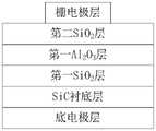
可选的,当X为Al元素时,氧化物固溶体薄膜选用Al2(SiO3)3薄膜,且控制精细分层的温度在525~575℃,精细分层的厚度在20~30nm下,所述Al2(SiO3)3薄膜被精细分成第一SiO2层、第一Al2O3层和第二SiO2层。Optionally, when X is an Al element, the oxide solid solution film is an Al2 (SiO3 )3 film, and the temperature of the fine layering is controlled at 525-575°C, and the thickness of the fine layering is 20-30 nm. The Al2 (SiO3 )3 thin film is finely divided into a first SiO2 layer, a first Al2 O3 layer and a second SiO2 layer.
可选的,当A为Al元素时,氧化物固溶体薄膜选用Al2(SiO3)3薄膜,且控制精细分层的温度在600~700℃下,精细分层的厚度在20~30nm下,所述Al2(SiO3)3薄膜被精细分成第一SiO2层、第一Al2O3层、第三SiO2层和第二Al2O3层。Optionally, when A is Al element, the oxide solid solution film is selected from Al2 (SiO3 )3 film, and the temperature of the fine layering is controlled at 600-700° C., and the thickness of the fine layering is 20-30 nm. The Al2 (SiO3 )3 thin film is finely divided into a first SiO2 layer, a first Al2 O3 layer, a third SiO2 layer and a second Al2 O3 layer.
可选的,当A为Al元素时,氧化物固溶体薄膜选用Al2(SiO3)3薄膜,且控制精细分层的温度在600~700℃,精细分层的厚度在35~45nm下,所述Al2(SiO3)3薄膜被精细分成第一SiO2层、第一Al2O3层、第二SiO2层和第二Al2O3层。Optionally, when A is Al element, the oxide solid solution film is selected from Al2 (SiO3 )3 film, and the temperature of the fine stratification is controlled at 600-700° C., and the thickness of the fine stratification is 35-45 nm. The Al2 (SiO3 )3 thin film is finely divided into a first SiO2 layer, a first Al2 O3 layer, a second SiO2 layer and a second Al2 O3 layer.
可选的,当A为Zr元素时,氧化物固溶体薄膜选用ZrSiO4薄膜,且控制精细分层的温度在600~800℃,精细分层的厚度在20~35nm下,所述ZrSiO4薄膜被精细分成第一SiO2层、ZrO2层和第二SiO2层。Optionally, when A is the Zr element, the oxide solid solution film is a ZrSiO4 film, and the temperature of the fine layering is controlled at 600-800 °C, and the thickness of the fine layering is 20-35 nm, and the ZrSiO4 film is Finely divided into a first SiO2 layer, a ZrO2 layer and a second SiO2 layer.
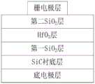
可选的,当A为Hf元素时,氧化物固溶体薄膜选用HfSiO4薄膜,且控制精细分层的温度在700~900℃,精细分层的厚度在20~35nm下,所述HfSiO4薄膜被精细分成第一SiO2层、HfO2层和第二SiO2层。Optionally, when A is Hf element, HfSiO4 film is selected as the oxide solid solution film, and the temperature of the fine layering is controlled at 700-900°C, and the thickness of the fine layering is 20-35 nm, and the HfSiO4 film is Finely divided into a first SiO2 layer, a HfO2 layer and a second SiO2 layer.
可选的,所述精细分层的氧气压力控制在1.5~2.5Pa。Optionally, the oxygen pressure of the fine layering is controlled at 1.5-2.5Pa.
一种SiC功率器件,包括第一电极层、第二电极层、SiC衬底层和分相层,所述分相层设置在SiC衬底层上,所述第二电极层设置在SiC衬底层远离分相层的一端面,所述第一电极层设置在所述分相层远离SiC衬底层的一端面。A SiC power device, comprising a first electrode layer, a second electrode layer, a SiC substrate layer and a phase separation layer, the phase separation layer is arranged on the SiC substrate layer, and the second electrode layer is arranged on the SiC substrate layer away from the separation layer. One end face of the phase layer, the first electrode layer is disposed on one end face of the phase separation layer away from the SiC substrate layer.
可选的,所述第一电极层为多晶硅材料或金属材料,所述第二电极层为金属材料。Optionally, the first electrode layer is a polysilicon material or a metal material, and the second electrode layer is a metal material.
采用本申请提供的技术方案,与现有技术相比,具有如下有益效果:Adopting the technical scheme provided by the application, compared with the prior art, has the following beneficial effects:
通过将氧化物固溶体薄膜在设定的温度范围以及氧气压力下进行精细分层,从而得到分相层,并且通过分相层与SiC衬底层的接触,增加了SiC衬底层的界面价带差距和导带差距,从而抑制漏电流,降低了能量损耗,防止在栅压作用下,电子跨过势垒,产生较大隧穿电流,造成较大的能量损耗,而500~900℃的温度设置,低于传统的退火温度设置,从而使得在SiC衬底层的界面处不易形成例如Si-Si键和C-C键的碳团簇,进而使界面载流子拥有较高的迁移率。By finely layering the oxide solid solution film under a set temperature range and oxygen pressure, a phase-separated layer is obtained, and through the contact between the phase-separated layer and the SiC substrate layer, the interfacial valence band gap of the SiC substrate layer is increased. The conduction band gap can suppress leakage current, reduce energy loss, and prevent electrons from crossing the potential barrier under the action of gate voltage, resulting in large tunneling current and large energy loss. Lower than the conventional annealing temperature setting, carbon clusters such as Si-Si bonds and C-C bonds are not easily formed at the interface of the SiC substrate layer, thereby enabling interface carriers to have higher mobility.
附图说明Description of drawings
为了更清楚地说明本申请实施例或现有技术中的技术方案,下面将对实施例或现有技术描述中所需要使用的附图作简单地介绍,显而易见地,下面描述中的附图仅仅是本申请的一些实施例,对于本领域普通技术人员来讲,在不付出创造性劳动性的前提下,还可以根据这些附图获得其他的附图。In order to more clearly illustrate the embodiments of the present application or the technical solutions in the prior art, the following briefly introduces the accompanying drawings required for the description of the embodiments or the prior art. Obviously, the drawings in the following description are only These are some embodiments of the present application. For those of ordinary skill in the art, other drawings can also be obtained based on these drawings without any creative effort.
图1为本申请提出的一种SiC功率器件的制备方法的流程图;Fig. 1 is the flow chart of the preparation method of a kind of SiC power device proposed by the application;
图2为本实施例一提出的一种SiC功率器件的制备方法得到的SiC功率器件结构图;2 is a structural diagram of a SiC power device obtained by a method for preparing a SiC power device proposed in the first embodiment;
图3为本实施例一提出的SiC功率器件的能带变化图以及传统SiC功率器件的能带变化图;FIG. 3 is an energy band change diagram of the SiC power device proposed in the first embodiment and an energy band change diagram of a traditional SiC power device;
图4为本实施例二提出的一种SiC功率器件的制备方法得到的SiC功率器件结构图;4 is a structural diagram of a SiC power device obtained by a method for preparing a SiC power device proposed in the second embodiment;
图5为本实施例三提出的一种SiC功率器件的制备方法得到的SiC功率器件结构图;5 is a structural diagram of a SiC power device obtained by a method for preparing a SiC power device proposed in the third embodiment;
图6为本实施例四提出的一种SiC功率器件的制备方法得到的SiC功率器件结构图;6 is a structural diagram of a SiC power device obtained by a method for preparing a SiC power device proposed in the fourth embodiment;
图7为本实施例五提出的一种SiC功率器件的制备方法得到的SiC功率器件结构图。FIG. 7 is a structural diagram of a SiC power device obtained by a method for fabricating a SiC power device proposed in the fifth embodiment.
具体实施方式Detailed ways
下面结合实施例对本申请做进一步的详细说明,以下实施例是对本申请的解释而本申请并不局限于以下实施例。The present application will be further described in detail below with reference to the examples. The following examples are to explain the present application and the present application is not limited to the following examples.
实施例一Example 1
如图1所示,一种SiC功率器件的制备方法,包括以下步骤:首先使用清洗气体一对SiC衬底层的晶面缺陷进行清洗;其中清洗气体一可以为氢气,且在对SiC衬底层进行清洗时,清洗温度设置为500℃。As shown in FIG. 1 , a method for preparing a SiC power device includes the following steps: first, a cleaning gas is used to clean the crystal plane defects of a SiC substrate layer; During cleaning, the cleaning temperature was set to 500°C.
清洗完SiC衬底层表面的晶面缺陷后,通过等离子体增强原子层沉积的方法,又称PECVD方法,在SiC衬底层上生长氧化物固溶体薄膜,且氧化物固溶体薄膜的厚度为20~50nm,其中,氧化物固溶体薄膜为AxSiOy薄膜,A为a价元素,且满足4+ax=2y,而A可为Al、Zr、Hf、Y、Ta或La等元素。After cleaning the crystal plane defects on the surface of the SiC substrate layer, the oxide solid solution film is grown on the SiC substrate layer by the plasma enhanced atomic layer deposition method, also known as the PECVD method, and the thickness of the oxide solid solution film is 20-50nm. The oxide solid solution thin film is an Ax SiOy thin film, A is a valence element, and satisfies 4+ax=2y, and A can be an element such as Al, Zr, Hf, Y, Ta, or La.
由于考虑高介电材料自身的介电常数相较于SiO2较大,而所获得的SiO2等效厚度约为1~10nm,根据Al2O3、ZrO2和HfO2自身的相对介电常数分别为9.0、25和25,其物理厚度可相较于SiO2等效厚度的2至6倍,因此氧化物固溶体薄膜整体厚度设置为20~50nm。Considering that the dielectric constant of the high dielectric material itself is larger than that of SiO2 , the obtained equivalent thickness of SiO2 is about 1-10 nm. According to the relative dielectrics of Al2 O3 , ZrO2 and HfO2 themselves The constants are 9.0, 25, and 25, respectively, and their physical thickness can be compared to 2 to 6 times the equivalent thickness of SiO2 , so the overall thickness of the oxide solid solution film is set to 20 to 50 nm.
基于Al2O3、ZrO2和HfO2结晶温度不同的情况,因此,在氮气环境下对氧化物固溶体薄膜进行精细分层,得到分相层,并通过精细分层过程中调节精细分层的温度以及氧气压力,使得在不同的温度区间,氧化物固溶体薄膜会自组装结晶形成单独的薄膜,同时在氧气压力下,使得分相层靠近SiC衬底层处出现不同膜层厚度,其中,精细分层的温度为500~900℃,精细分层的氧气压力为1.5~2.5Pa。Based on the different crystallization temperatures of Al2 O3 , ZrO2 and HfO2 , the oxide solid solution thin films were finely stratified in a nitrogen atmosphere to obtain a phase-separated layer, and the fine stratification was adjusted during the fine stratification process The temperature and oxygen pressure make the oxide solid solution film self-assemble and crystallize to form a separate film in different temperature ranges. At the same time, under the oxygen pressure, different film thicknesses appear in the phase separation layer near the SiC substrate layer. The temperature of the layer is 500-900°C, and the oxygen pressure of the fine layering is 1.5-2.5Pa.
其中,Al2O3、ZrO2和HfO2又可称为高介氧化物,由于Al2O3、ZrO2和HfO2自身的能带间隙分别为8.7eV、7.8eV、5.7eV,其在与能带间隙3.3eV的4H-SiC形成界面的过程中,价带差距以及导带差距明显小于能带间隙为8.9eV的SiO2,容易造成较大的漏电流,而通过计算发现,在高介氧化物与SiC间插入一层SiO2时,其整体价带差距和导带差距将被显著拉大,但是考虑到SiO2的等效厚度较大,其物理厚度应尽可能小,因此综合考虑SiO2的有效性和对栅极漏电流的抑制,最靠近SiC衬底层的第一SiO2层薄膜的物理厚度需要控制到1-5nm以内,方能达到静态功耗下降的目的。Among them, Al2 O3 , ZrO2 and HfO2 can also be called high dielectric oxides. Since the energy band gaps of Al2 O3 , ZrO2 and HfO2 are 8.7eV, 7.8eV, and 5.7eV, respectively, In the process of forming the interface with 4H-SiC with a band gap of 3.3 eV, the valence band gap and conduction band gap are significantly smaller than those of SiO2 with a band gap of 8.9 eV, which is easy to cause a large leakage current. When a layer of SiO2 is inserted between the dielectric oxide and SiC, the overall valence band gap and conduction band gap will be significantly enlarged, but considering the large equivalent thickness of SiO2 , its physical thickness should be as small as possible. Considering the effectiveness of SiO2 and the suppression of gate leakage current, the physical thickness of the first SiO2 layer film closest to the SiC substrate layer needs to be controlled within 1-5 nm to achieve the purpose of reducing static power consumption.
如图2所示,当A为Al元素时,氧化物固溶体薄膜选用Al2(SiO3)3薄膜,此时先将Al2(SiO3)3薄膜生长在SiC衬底层上,且控制精细分层的温度在525~575℃,精细分层的厚度在20~30nm下,精细分层的氧气压力控制在1.5~2.5Pa,Al2(SiO3)3薄膜被精细分成第一SiO2层、第一Al2O3层和第二SiO2层,具体的,本实施例选用Al2(SiO3)3薄膜的厚度为30nm,控制精细分层的温度保持在550℃,精细分层的氧气压力控制保持在1.5Pa,此时,精细分层后得到分相层,且分相层共有三层,即Al2(SiO3)3薄膜被精细分成第一SiO2层、第一Al2O3层和第二SiO2层,其中第一SiO2层为靠近SiC衬底层的一层,且分相得到的厚度为2nm,满足1-5nm的要求,实现了静态功耗下降的目的,而得到的第一Al2O3层的厚度为20nm,得到的第二SiO2层的厚度为20nm。As shown in Figure 2, when A is Al element, Al2 (SiO3 )3 thin film is selected as the oxide solid solution thin film. At this time, the Al2 (SiO3 )3 thin film is first grown on the SiC substrate layer, and the fine separation is controlled. The temperature of the layer is 525~575℃, the thickness of the fine layer is 20~30nm, the oxygen pressure of the fine layer is controlled at 1.5~2.5Pa, and the Al2 (SiO3 )3 film is finely divided into the first SiO2 layer, The first Al2 O3 layer and the second SiO2 layer, specifically, in this embodiment, the thickness of the Al2 (SiO3 )3 film is selected to be 30 nm, the temperature of the fine stratification is controlled to be kept at 550° C., and the fine stratified oxygen The pressure is kept at 1.5Pa. At this time, a phase separation layer is obtained after fine layering, and the phase separation layer has three layers, namely, the Al2 (SiO3 )3 film is finely divided into the first SiO2 layer, the first Al2 O3 layers and the second SiO2 layer, wherein the first SiO2 layer is a layer close to the SiC substrate layer, and the thickness obtained by phase separation is 2nm, which meets the requirements of 1-5nm, and achieves the purpose of reducing static power consumption, while The thickness of the obtained first Al2 O3 layer was 20 nm, and the thickness of the obtained second SiO2 layer was 20 nm.
一方面,由于在精细分层过程中,不涉及对SiC衬底层的直接氧化,且退火温度控制在600~900℃,温度较低,因此不容易在SiC衬底层的界面处形成碳团簇,例如Si-Si键和C-C键,使得界面载流子拥有较高的迁移率,同时精细分层后得到的第一SiO2层与SiC衬底层接触,还可增加SiC衬底层的界面价带差距和导带差距,从而抑制漏电流,防止在栅压作用下,电子跨过势垒,产生较大隧穿电流,造成较大的能量损耗。On the one hand, since the process of fine layering does not involve direct oxidation of the SiC substrate layer, and the annealing temperature is controlled at 600-900 °C, the temperature is relatively low, so it is not easy to form carbon clusters at the interface of the SiC substrate layer. For example, Si-Si bonds and CC bonds make the interface carriers have higher mobility, and the first SiO2 layer obtained after fine layering is in contact with the SiC substrate layer, which can also increase the interface valence band gap of the SiC substrate layer. and the conduction band gap, thereby suppressing leakage current and preventing electrons from crossing the potential barrier under the action of gate voltage, resulting in large tunneling current and large energy loss.
如图3所示,ΔEv表示价带差距,ΔEc表示导带差距,由图可知,通过精细分层后得到的SiC/SiO2/High-k结构所测得的价带差距比SiC/High-k结构测得的价带差距大,同样的,SiC/SiO2/High-k结构所测得的导带差距比SiC/High-k结构测得的导带差距大,其中High-k为高k金属栅材料,从而在实际检测中证明了本实施例所要达到的增加界面价带、导带差距的目的,进而抑制了漏电流。As shown in Figure 3, ΔEv represents the valence band gap, and ΔEc represents the conduction band gap. It can be seen from the figure that the valence band gap measured by the SiC/SiO2 /High-k structure obtained after fine layering is higher than that of SiC/High- The valence band gap measured by the k structure is large. Similarly, the conduction band gap measured by the SiC/SiO2 /High-k structure is larger than the conduction band gap measured by the SiC/High-k structure, where High-k is high. k metal gate material, so that the purpose of increasing the interface valence band and conduction band gap to be achieved by this embodiment is proved in actual testing, thereby suppressing the leakage current.
另一方面,通过控制氧化物固溶体薄膜的生长过程的温度及氧气压力,控制分相后生成的高介电氧化物与SiO2的厚度比例,从而使整体介电常数大于8,从而减小电场,使整体结构更可靠。On the other hand, by controlling the temperature and oxygen pressure in the growth process of the oxide solid solution film, the thickness ratio of the high dielectric oxide andSiO2 generated after phase separation is controlled, so that the overall dielectric constant is greater than 8, thereby reducing the electric field , making the overall structure more reliable.
得到第一SiO2层、第一Al2O3层和第二SiO2层后,使用清洗气体二对分相层的悬挂键钝化和悬挂键缺陷进行清洗,其中清洗气体而可以为一氧化二氮,且清洗温度设置为500℃,最后采用磁控溅射法在分相层上沉积第一电极层,在SiC衬底层上沉积第二电极层。After the first SiO2 layer, the first Al2 O3 layer and the second SiO2 layer are obtained, the dangling bond passivation and dangling bond defects of the phase-separated layer are cleaned by two cleaning gases, wherein the cleaning gas can be monoxide Dinitrogen, and the cleaning temperature is set to 500° C., finally, a first electrode layer is deposited on the phase separation layer by a magnetron sputtering method, and a second electrode layer is deposited on the SiC substrate layer.
实施例二Embodiment 2
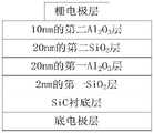
如图4所示,本实施与实施例一相比,其区别在于,对厚度为30nm的Al2(SiO3)3薄膜进行精细分层时,通过控制精细分层的温度在600~700℃下,使得Al2(SiO3)3薄膜被精细分成第一SiO2层、第一Al2O3层、第三SiO2层和第二Al2O3层,最优的,控制精细分层的温度保持在600℃,精细分层的氧气压力同样选用1.5Pa,此时,精细分层后的分相层共四层,即Al2(SiO3)3薄膜被精细分成2nm的第一SiO2层、20nm的第一Al2O3层、10nm的第三SiO2层和10nm的第二Al2O3层。As shown in FIG. 4 , the difference between this embodiment and the first embodiment is that when fine layering is performed on an Al2 (SiO3 )3 film with a thickness of 30 nm, the temperature of the fine layering is controlled at 600-700° C. Next, the Al2 (SiO3 )3 thin film is finely divided into a first SiO2 layer, a first Al2 O3 layer, a third SiO2 layer and a second Al2 O3 layer, and optimally, the fine layering is controlled The temperature is kept at 600°C, and the oxygen pressure of the fine layering is also selected as 1.5Pa. At this time, the phase separation layer after the fine layering has a total of four layers, that is, the Al2 (SiO3 )3 film is finely divided into 2nm first SiO layers2 layers, a 20nm firstAl2O3 layer, a 10nm thirdSiO2 layer and a10nmsecondAl2O3 layer.
此时达到高介电常数材料层与SiO2层周期性交替排列的目的,即由靠近SiC衬底层开始,依次为SiO2材料、Al2O3材料、SiO2材料、Al2O3材料,其中,满足在第一Al2O3层与SiC衬底层之间插入第一SiO2层,以保证整体价带差距和导带差距显著拉大的情况下,还使得最靠近SiC衬底层的第一SiO2层的厚度为2nm,控制到了1-5nm以内,从而实现了静态功耗降低的目的,避免了传统的能带间隙为8.7eV的Al2O3与能带间隙为3.3eV的4H-SiC形成界面的过程中,价带差距以及导带差距过小,导致产生较大漏电流的现象发生,而由于本实施例所使用的精细分层的温度较低,为600℃,因此在SiC衬底层的界面处不易形成例如Si-Si键和C-C键的碳团簇,从而使得界面载流子拥有较高的迁移率。At this time, the purpose of periodically alternating the high dielectric constant material layer and the SiO2 layer is achieved, that is, starting from the SiC substrate layer, followed by SiO2 material, Al2 O3 material, SiO2 material, Al2 O3 material, Wherein, it is satisfied that the first SiO2 layer is inserted between the first Al2 O3 layer and the SiC substrate layer, so as to ensure that the overall valence band gap and conduction band gap are significantly enlarged, and the first layer closest to the SiC substrate layer is also made. The thickness of aSiO2 layer is 2nm, which is controlled to within 1-5nm, thus achieving the purpose of reducing static power consumption, avoiding the traditionalAl2O3 with a bandgap of8.7eV and 4H with a bandgap of 3.3eV -In the process of forming the interface with SiC, the valence band gap and the conduction band gap are too small, resulting in the phenomenon of large leakage current. Since the temperature of the fine layering used in this embodiment is low, which is 600 °C, it is Carbon clusters such as Si-Si bonds and CC bonds are not easily formed at the interface of the SiC substrate layer, so that the interface carriers have higher mobility.
与实施例一相同的是,由于对Al2(SiO3)3薄膜的生长过程的温度及氧气压力进行了控制,从而控制了分相后生成的高介电氧化物与SiO2的厚度比例,使得本实施例最后所得的栅氧结构整体介电常数大于8,从而减小电场,使整体结构更可靠,另一方面,Al2(SiO3)3薄膜精细分层后得到的2nm的第一SiO2层与SiC衬底层接触,同样的增加了SiC衬底层的界面价带差距和导带差距,从而抑制漏电流,防止在栅压作用下,电子跨过势垒,产生较大隧穿电流,造成较大的能量损耗。The same as the first embodiment, due to the control of the temperature and oxygen pressure in the growth process of the Al2 (SiO3 )3 film, the thickness ratio of the high dielectric oxide and SiO2 generated after the phase separation is controlled,The overall dielectric constantof the gateoxide structure finally obtained in this embodiment is greater than 8, thereby reducing the electric field and making the overall structure more reliable. The SiO2 layer is in contact with the SiC substrate layer, which also increases the interface valence band gap and conduction band gap of the SiC substrate layer, thereby suppressing leakage current and preventing electrons from crossing the potential barrier under the action of gate voltage, resulting in a large tunneling current. , resulting in a large energy loss.
实施例三Embodiment 3
如图5所示,本实施例与实施例一相比,其区别在于,通过控制精细分层的温度在600~700℃,且精细分层的厚度在35~45nm下,从而使Al2(SiO3)3薄膜被精细分成第一SiO2层、第一Al2O3层、第二SiO2层和第二Al2O3层,此时最优的,同样的控制精细分层的温度保持在600℃,精细分层的氧气压力选用1.5Pa,此时,精细分层后的分相层共四层,即Al2(SiO3)3薄膜被精细分成2nm的第一SiO2层、20nm的第一Al2O3层、20nm的第二SiO2层和10nm的第二Al2O3层。As shown in FIG. 5 , the difference between this embodiment and the first embodiment is that the temperature of the fine layering is controlled at 600-700° C., and the thickness of the fine layering is at 35-45 nm, so that the Al2 ( The SiO3 )3 thin film is finely divided into a first SiO2 layer, a first Al2 O3 layer, a second SiO2 layer and a second Al2 O3 layer. At this time, it is optimal to control the temperature of the fine layering. Maintained at 600 ° C, the oxygen pressure of fine layering was selected as 1.5Pa. At this time, the phase separation layer after fine layering was divided into four layers, that is, the Al2 (SiO3 )3 film was finely divided into the first SiO2 layer of 2 nm, 20nm firstAl2O3 layer, 20nmsecondSiO2 layer and 10nmsecondAl2O3 layer.
此时达到高介电常数材料层与SiO2层周期性交替排列的目的,即由靠近SiC衬底层开始,依次为SiO2材料、Al2O3材料、SiO2材料、Al2O3材料,其中,满足在第一Al2O3层与SiC衬底层之间插入第一SiO2层,以保证整体价带差距和导带差距显著拉大的情况下,还使得最靠近SiC衬底层的第一SiO2层的厚度为2nm,控制到了1-5nm以内,从而实现了静态功耗降低的目的,避免了传统的能带间隙为8.7eV的Al2O3与能带间隙为3.3eV的4H-SiC形成界面的过程中,价带差距以及导带差距过小,导致产生较大漏电流的现象发生,而由于本实施例所使用的精细分层的温度较低,为600℃,因此在SiC衬底层的界面处不易形成例如Si-Si键和C-C键的碳团簇,从而使得界面载流子拥有较高的迁移率。At this time, the purpose of periodically alternating the high dielectric constant material layer and the SiO2 layer is achieved, that is, starting from the SiC substrate layer, followed by SiO2 material, Al2 O3 material, SiO2 material, Al2 O3 material, Wherein, it is satisfied that the first SiO2 layer is inserted between the first Al2 O3 layer and the SiC substrate layer, so as to ensure that the overall valence band gap and conduction band gap are significantly enlarged, and the first layer closest to the SiC substrate layer is also made. The thickness of aSiO2 layer is 2nm, which is controlled to within 1-5nm, thus achieving the purpose of reducing static power consumption, avoiding the traditionalAl2O3 with a bandgap of8.7eV and 4H with a bandgap of 3.3eV -In the process of forming the interface with SiC, the valence band gap and the conduction band gap are too small, resulting in the phenomenon of large leakage current. Since the temperature of the fine layering used in this embodiment is low, which is 600 °C, it is Carbon clusters such as Si-Si bonds and CC bonds are not easily formed at the interface of the SiC substrate layer, so that the interface carriers have higher mobility.
与实施例二相同的是,由于对Al2(SiO3)3薄膜的生长过程的温度及氧气压力进行了控制,从而控制了分相后生成的高介电氧化物与SiO2的厚度比例,使得本实施例最后所得的栅氧结构整体介电常数大于8,从而减小电场,使整体结构更可靠,另一方面,Al2(SiO3)3薄膜精细分层后得到的2nm的第一SiO2层与SiC衬底层接触,同样的增加了SiC衬底层的界面价带差距和导带差距,从而抑制漏电流,防止在栅压作用下,电子跨过势垒,产生较大隧穿电流,造成较大的能量损耗。Same as the second embodiment, because the temperature and oxygen pressure in the growth process of the Al2 (SiO3 )3 film are controlled, the thickness ratio of the high dielectric oxide and SiO2 generated after the phase separation is controlled,The overall dielectric constantof the gateoxide structure finally obtained in this embodiment is greater than 8, thereby reducing the electric field and making the overall structure more reliable. The SiO2 layer is in contact with the SiC substrate layer, which also increases the interface valence band gap and conduction band gap of the SiC substrate layer, thereby suppressing leakage current and preventing electrons from crossing the potential barrier under the action of gate voltage, resulting in a large tunneling current. , resulting in a large energy loss.
实施例四Embodiment 4
如图6所示,当A为Zr元素时,氧化物固溶体薄膜选用ZrSiO4薄膜,且控制精细分层的温度在600~800℃,精细分层的厚度在20~35nm下,从而ZrSiO4薄膜被精细分成第一SiO2层、ZrO2层和第二SiO2层,最优的,控制ZrSiO4薄膜的厚度为30nm,此时控制精细分层的温度保持在700℃,精细分层的氧气压力同样选用1.5Pa,此时,精细分层后的分相层共三层,即ZrSiO4薄膜被精细分成2nm的第一SiO2层、20nm的ZrO2层和20nm的第二SiO2层。As shown in Figure 6, when A is Zr element, ZrSiO4 thin film is selected for oxide solid solution film, and the temperature of fine layering is controlled at 600-800 °C, and the thickness of fine layering is 20-35 nm, so that ZrSiO4 thin film It is finely divided into a firstSiO2 layer, a ZrO2 layer and asecondSiO2 layer.The optimal, the thickness of the ZrSiO4 film is controlled to be 30 nm, and the temperature of the finely layered layer is kept at 700 °C, and the finely layered oxygen The pressure is also selected as 1.5Pa. At this time, the finely delaminated phase-separated layers are divided intothree layers, namely, the ZrSiO4 film is finely divided into the firstSiO2 layer of 2nm, the ZrO2 layer of 20nm and thesecondSiO2 layer of 20nm.
其中,满足在ZrO2层与SiC衬底层之间插入第一SiO2层,以保证整体价带差距和导带差距显著拉大的情况下,还使得最靠近SiC衬底层的第一SiO2层的厚度为2nm,控制到了1-5nm以内,从而实现了静态功耗降低的目的,避免了传统的能带间隙为7.8eV的ZrO2与能带间隙为3.3eV的4H-SiC形成界面的过程中,价带差距以及导带差距过小,导致产生较大漏电流的现象发生,而由于本实施例所使用的精细分层的温度较低,为700℃,因此在SiC衬底层的界面处不易形成例如Si-Si键和C-C键的碳团簇,从而使得界面载流子拥有较高的迁移率。Wherein, it is satisfied that the first SiO2 layer is inserted between the ZrO2 layer and the SiC substrate layer to ensure that the overall valence band gap and conduction band gap are significantly enlarged, and the first SiO2 layer closest to the SiC substrate layer is also made. The thickness is 2nm, which is controlled to within 1-5nm, so as to achieve the purpose of reducing static power consumption and avoid the traditional process of forming the interface between ZrO2 with a band gap of 7.8eV and 4H-SiC with a band gap of 3.3eV , the valence band gap and the conduction band gap are too small, resulting in the phenomenon of large leakage current. Since the temperature of the fine layering used in this embodiment is relatively low, which is 700 ° C, the interface of the SiC substrate layer is It is difficult to form carbon clusters such as Si-Si bonds and CC bonds, so that the interface carriers have higher mobility.
与实施例一相同的是,由于对ZrSiO4薄膜的生长过程的温度及氧气压力进行了控制,从而控制了分相后生成的高介电氧化物ZrO2与SiO2的厚度比例,使得本实施例最后所得的栅氧结构整体介电常数大于8,从而减小电场,使整体结构更可靠,另一方面,ZrSiO4薄膜精细分层后得到的2nm的第一SiO2层与SiC衬底层接触,同样的增加了SiC衬底层的界面价带差距和导带差距,从而抑制漏电流,防止在栅压作用下,电子跨过势垒,产生较大隧穿电流,造成较大的能量损耗。Same as the first embodiment, because the temperature and oxygen pressure in the growth process of the ZrSiO4 film are controlled, the thickness ratio of the high dielectric oxide ZrO2 and SiO2 generated after the phase separation is controlled, so that this embodiment Example The overall dielectric constant of the gate oxide structure finally obtained is greater than 8, thereby reducing the electric field and making the overall structure more reliable. On the other hand, the firstSiO2 layer of2 nm obtained after the fine layering of the ZrSiO4 film is in contact with the SiC substrate layer. , which also increases the interface valence band gap and conduction band gap of the SiC substrate layer, thereby suppressing leakage current and preventing electrons from crossing the potential barrier under the action of gate voltage, resulting in large tunneling current and large energy loss.
实施例五Embodiment 5
如图7所示,当A为Hf元素时,氧化物固溶体薄膜选用HfSiO4薄膜,从而控制精细分层的温度在700~900℃,精细分层的厚度在20~35nm下,使得HfSiO4薄膜被精细分成第一SiO2层、HfO2层和第二SiO2层,最优的,控制HfSiO4薄膜的厚度为30nm,此时控制精细分层的温度为850℃,精细分层的氧气压力同样选用1.5Pa,此时,精细分层后的分相层共三层,即HfSiO4薄膜被精细分成2nm的第一SiO2层、20nm的HfO2层和20nm的第二SiO2层。As shown in Figure 7, when A is Hf element, HfSiO4 film is selected as the oxide solid solution film, so that the temperature of fine layering is controlled at 700-900 °C, and the thickness of fine layering is 20-35 nm, so that the HfSiO4 film is It is finely divided into the firstSiO2 layer, theHfO2 layer and the secondSiO2 layer. The optimal, the thickness of theHfSiO4 film is controlled to be 30 nm, the temperature of the fine layered layer is controlled to be 850 °C, and the oxygen pressure of the fine layered layer is controlled at 30 nm. The same 1.5Pa is selected. At this time, the finely layered phase-separated layers are divided into three layers, namely, theHfSiO4 film is finely divided into a first SiO2 layer of 2nm, aHfO2 layer of 20nm and asecondSiO2 layer of 20nm.
其中,满足在HfO2层与SiC衬底层之间插入第一SiO2层,以保证整体价带差距和导带差距显著拉大的情况下,还使得最靠近SiC衬底层的第一SiO2层的厚度为2nm,控制到了1-5nm以内,从而实现了静态功耗降低的目的,避免了传统的能带间隙为5.7eV的HfO2与能带间隙为3.3eV的4H-SiC形成界面的过程中,价带差距以及导带差距过小,导致产生较大漏电流的现象发生,而由于本实施例所使用的精细分层的温度较低,为850℃,因此在SiC衬底层的界面处不易形成例如Si-Si键和C-C键的碳团簇,从而使得界面载流子拥有较高的迁移率。Wherein, it is satisfied that the first SiO2 layer is inserted between the HfO2 layer and the SiC substrate layer to ensure that the overall valence band gap and conduction band gap are significantly enlarged, and the first SiO2 layer closest to the SiC substrate layer is also made. The thickness is 2nm, which is controlled within 1-5nm, so as to achieve the purpose of reducing static power consumption and avoid the traditional process of forming the interface between HfO2 with a band gap of 5.7eV and 4H-SiC with a band gap of 3.3eV , the valence band gap and conduction band gap are too small, resulting in a large leakage current. Since the temperature of the fine layering used in this embodiment is relatively low, which is 850 °C, the interface of the SiC substrate layer is It is difficult to form carbon clusters such as Si-Si bonds and CC bonds, so that the interface carriers have higher mobility.
与实施例一相同的是,由于对HfSiO4薄膜的生长过程的温度及氧气压力进行了控制,从而控制了分相后生成的高介电氧化物HfO2与SiO2的厚度比例,使得本实施例最后所得的栅氧结构整体介电常数大于8,从而减小电场,使整体结构更可靠,另一方面,HfSiO4薄膜精细分层后得到的2nm的第一SiO2层与SiC衬底层接触,同样的增加了SiC衬底层的界面价带差距和导带差距,从而抑制漏电流,防止在栅压作用下,电子跨过势垒,产生较大隧穿电流,造成较大的能量损耗。Same as the first embodiment, because the temperature and oxygen pressure in the growth process of the HfSiO4 film are controlled, the thickness ratio of the high dielectric oxide HfO2 and SiO2 generated after the phase separation is controlled, so that this embodiment Example The overall dielectric constant of the gate oxide structure finally obtained is greater than 8, thereby reducing the electric field and making the overall structure more reliable. On the other hand, the firstSiO2 layer of 2 nm obtained after fine layering of theHfSiO4 film is in contact with the SiC substrate layer. , which also increases the interface valence band gap and conduction band gap of the SiC substrate layer, thereby suppressing leakage current and preventing electrons from crossing the potential barrier under the action of gate voltage, resulting in large tunneling current and large energy loss.
实施例六Embodiment 6
一种SiC功率器件,包括第一电极层、第二电极层、SiC衬底层和分相层,分相层设置在SiC衬底层上,第二电极层设置在SiC衬底层远离分相层的一端面,第一电极层设置在分相层远离SiC衬底层的一端面,其中第一电极层为多晶硅材料或金属材料,第二电极层为金属材料,金属材料可以为镍或铝。A SiC power device, comprising a first electrode layer, a second electrode layer, a SiC substrate layer and a phase separation layer, the phase separation layer is arranged on the SiC substrate layer, and the second electrode layer is arranged on a SiC substrate layer away from the phase separation layer. The end face, the first electrode layer is disposed on the end face of the phase separation layer away from the SiC substrate layer, wherein the first electrode layer is polysilicon material or metal material, the second electrode layer is metal material, and the metal material can be nickel or aluminum.
通过分相层的设置,并且使得分相层与SiC衬底层的接触,增加了SiC衬底层的界面价带差距和导带差距,从而抑制漏电流,降低了能量损耗,防止在栅压作用下,电子跨过势垒,产生较大隧穿电流,造成较大的能量损耗。Through the setting of the phase separation layer and the contact between the phase separation layer and the SiC substrate layer, the interface valence band gap and conduction band gap of the SiC substrate layer are increased, thereby suppressing the leakage current, reducing the energy loss and preventing the gate voltage. , the electrons cross the potential barrier, resulting in a large tunneling current, resulting in a large energy loss.
此外,需要说明的是,本说明书中所描述的具体实施例,其零、部件的形状、所取名称等可以不同。凡依本申请专利构思所述的构造、特征及原理所做的等效或简单变化,均包括于本申请专利的保护范围内。本申请所属技术领域的技术人员可以对所描述的具体实施例做各种各样的修改或补充或采用类似的方式替代,只要不偏离本申请的结构或者超越本权利要求书所定义的范围,均应属于本申请的保护范围。In addition, it should be noted that, in the specific embodiments described in this specification, the shapes and names of parts and components thereof may be different. All equivalent or simple changes made according to the structures, features and principles described in the patent concept of the present application are included in the protection scope of the patent of the present application. Those skilled in the art to which this application pertains can make various modifications or additions to the specific embodiments described or substitute in similar manners, as long as they do not deviate from the structure of the application or go beyond the scope defined by the claims, All should belong to the protection scope of this application.
Claims (10)
Translated fromChinesePriority Applications (1)
| Application Number | Priority Date | Filing Date | Title |
|---|---|---|---|
| CN202111614210.6ACN114300350A (en) | 2021-12-27 | 2021-12-27 | Preparation method of SiC power device and SiC power device |
Applications Claiming Priority (1)
| Application Number | Priority Date | Filing Date | Title |
|---|---|---|---|
| CN202111614210.6ACN114300350A (en) | 2021-12-27 | 2021-12-27 | Preparation method of SiC power device and SiC power device |
Publications (1)
| Publication Number | Publication Date |
|---|---|
| CN114300350Atrue CN114300350A (en) | 2022-04-08 |
Family
ID=80969879
Family Applications (1)
| Application Number | Title | Priority Date | Filing Date |
|---|---|---|---|
| CN202111614210.6APendingCN114300350A (en) | 2021-12-27 | 2021-12-27 | Preparation method of SiC power device and SiC power device |
Country Status (1)
| Country | Link |
|---|---|
| CN (1) | CN114300350A (en) |
Citations (8)
| Publication number | Priority date | Publication date | Assignee | Title |
|---|---|---|---|---|
| US20030080384A1 (en)* | 2001-10-25 | 2003-05-01 | Matsushita Electric Industrial Co.., Ltd. | Semiconductor substrate, semiconductor device and method for fabricating the same |
| CN1599961A (en)* | 2001-11-30 | 2005-03-23 | 松下电器产业株式会社 | Semiconductor device and manufacturing method thereof |
| CN103887163A (en)* | 2014-04-03 | 2014-06-25 | 中国科学院半导体研究所 | Manufacturing method for SiC-based MOS device gate dielectric thin film |
| CN104600127A (en)* | 2015-01-07 | 2015-05-06 | 西安电子科技大学 | SiC MOS Capacitor and Manufacturing Method of Al2O3/LaScO3/SiO2 Stacked Gate Dielectric Layer |
| CN104617161A (en)* | 2015-01-07 | 2015-05-13 | 西安电子科技大学 | SiC MOS Capacitor and Manufacturing Method of Al2O3/La2O3/SiO2 Stacked Gate Dielectric Layer |
| CN104952917A (en)* | 2015-07-03 | 2015-09-30 | 电子科技大学 | A silicon carbide VDMOS device |
| CN106158601A (en)* | 2015-03-26 | 2016-11-23 | 比亚迪股份有限公司 | The gate dielectric layer structure of SiC base device and the forming method of gate dielectric layer |
| CN109686667A (en)* | 2019-01-25 | 2019-04-26 | 泰科天润半导体科技(北京)有限公司 | A kind of SiC base MOS device and its preparation method and application |
- 2021
- 2021-12-27CNCN202111614210.6Apatent/CN114300350A/enactivePending
Patent Citations (8)
| Publication number | Priority date | Publication date | Assignee | Title |
|---|---|---|---|---|
| US20030080384A1 (en)* | 2001-10-25 | 2003-05-01 | Matsushita Electric Industrial Co.., Ltd. | Semiconductor substrate, semiconductor device and method for fabricating the same |
| CN1599961A (en)* | 2001-11-30 | 2005-03-23 | 松下电器产业株式会社 | Semiconductor device and manufacturing method thereof |
| CN103887163A (en)* | 2014-04-03 | 2014-06-25 | 中国科学院半导体研究所 | Manufacturing method for SiC-based MOS device gate dielectric thin film |
| CN104600127A (en)* | 2015-01-07 | 2015-05-06 | 西安电子科技大学 | SiC MOS Capacitor and Manufacturing Method of Al2O3/LaScO3/SiO2 Stacked Gate Dielectric Layer |
| CN104617161A (en)* | 2015-01-07 | 2015-05-13 | 西安电子科技大学 | SiC MOS Capacitor and Manufacturing Method of Al2O3/La2O3/SiO2 Stacked Gate Dielectric Layer |
| CN106158601A (en)* | 2015-03-26 | 2016-11-23 | 比亚迪股份有限公司 | The gate dielectric layer structure of SiC base device and the forming method of gate dielectric layer |
| CN104952917A (en)* | 2015-07-03 | 2015-09-30 | 电子科技大学 | A silicon carbide VDMOS device |
| CN109686667A (en)* | 2019-01-25 | 2019-04-26 | 泰科天润半导体科技(北京)有限公司 | A kind of SiC base MOS device and its preparation method and application |
Non-Patent Citations (2)
| Title |
|---|
| LINHUA HUANG ET AL: "Characterization of Al2O3/LaAlO3/SiO2 Gate Stack on 4H-SiC After Post-Deposition Annealing", 《IEEE TRANSACTIONS ON ELECTRON DEVICES》, vol. 68, no. 4, 24 March 2021 (2021-03-24)* |
| ZHEN WANG ET AL: "Tuning the high-κ oxide (HfO 2 , ZrO 2 )/4H-SiC interface properties with a SiO 2 interlayer for power device applications", 《APPLIED SURFACE SCIENCE》, 3 June 2020 (2020-06-03)* |
Similar Documents
| Publication | Publication Date | Title |
|---|---|---|
| CN102779852B (en) | SiC vertical double diffusion metal oxide semiconductor structure (VDMOS) device with composite gate dielectric structure | |
| CN106910776B (en) | Large area molybdenum disulfide field effect transistor and its preparation based on high-k gate dielectric | |
| WO2015055108A1 (en) | Group-iii nitride semiconductor device and manufacturing method therefor | |
| CN102244108A (en) | Silicon carbide (SiC) metal oxide semiconductor (MOS) capacitor with composite dielectric layer and manufacturing method for SiC MOS capacitor with composite dielectric layer | |
| CN110649092A (en) | Two-dimensional material heterojunction back-gate negative capacitance tunneling transistor and preparation method | |
| CN104037239A (en) | SiC MOS (metal oxide semiconductor) capacitor and manufacturing method | |
| CN103346255A (en) | Heterojunction, ferroelectric tunnel junction and preparation method and application thereof | |
| CN114300533A (en) | A gate oxide structure and preparation method | |
| CN106571387A (en) | High K material-based stacked-gate AlGaN/GaN high-electron mobility MOS device | |
| TW202324736A (en) | Gate-all-around field effect transistor | |
| CN114300350A (en) | Preparation method of SiC power device and SiC power device | |
| CN104037238A (en) | SiC MOS (metal oxide semiconductor) capacitor and manufacturing method | |
| CN108400165A (en) | Low-power consumption gallium nitride base negative capacitance field-effect transistor and preparation method | |
| CN104576766A (en) | Al2O3/LaAlO3/SiO2 Stacked Gate Dielectric Layer SiC MOS Capacitor and Manufacturing Method | |
| Chen et al. | Study of Hf-Ti-O thin film as high-k gate dielectric and application for ETSOI MOSFETs | |
| CN116741817A (en) | Gate dielectric layer, structure, semiconductor device and preparation method thereof | |
| CN106783979B (en) | Based on Ga2O3Cap layer composite double-gate PMOSFET of material and preparation method thereof | |
| CN116387158A (en) | Preparation method of high-performance GaN MIS-HEMT | |
| JP4868910B2 (en) | Semiconductor device and manufacturing method thereof | |
| CN104617161A (en) | SiC MOS Capacitor and Manufacturing Method of Al2O3/La2O3/SiO2 Stacked Gate Dielectric Layer | |
| CN108172613A (en) | A zirconium-based gate dielectric material with high dielectric constant crystalline phase and its preparation method | |
| CN111863960A (en) | High-K material based AlGaN/GaN high electron mobility transistor and fabrication method | |
| CN104037240A (en) | SiC MOS (metal oxide semiconductor) capacitor and manufacturing method | |
| CN113690307B (en) | A Diamond Field Effect Transistor with Triple-Stacked Gate Dielectric Structure | |
| CN110797398B (en) | high-K oxide gate insulating layer MOS-HEMT device and preparation method thereof |
Legal Events
| Date | Code | Title | Description |
|---|---|---|---|
| PB01 | Publication | ||
| PB01 | Publication | ||
| SE01 | Entry into force of request for substantive examination | ||
| SE01 | Entry into force of request for substantive examination |