CN114220765B - Memory and method of making the same - Google Patents
Memory and method of making the sameDownload PDFInfo
- Publication number
- CN114220765B CN114220765BCN202210160600.9ACN202210160600ACN114220765BCN 114220765 BCN114220765 BCN 114220765BCN 202210160600 ACN202210160600 ACN 202210160600ACN 114220765 BCN114220765 BCN 114220765B
- Authority
- CN
- China
- Prior art keywords
- trench
- forming
- isolation structure
- substrate
- word line
- Prior art date
- Legal status (The legal status is an assumption and is not a legal conclusion. Google has not performed a legal analysis and makes no representation as to the accuracy of the status listed.)
- Active
Links
- 238000004519manufacturing processMethods0.000titleclaimsabstractdescription18
- 238000002955isolationMethods0.000claimsabstractdescription180
- 239000000758substrateSubstances0.000claimsabstractdescription137
- 238000000034methodMethods0.000claimsabstractdescription93
- 238000003860storageMethods0.000claimsabstractdescription55
- 239000010410layerSubstances0.000claimsdescription212
- 239000011241protective layerSubstances0.000claimsdescription60
- 239000003990capacitorSubstances0.000claimsdescription43
- 239000011810insulating materialSubstances0.000claimsdescription28
- 239000004020conductorSubstances0.000claimsdescription18
- 125000006850spacer groupChemical group0.000claimsdescription10
- 238000011049fillingMethods0.000claimsdescription7
- 230000003647oxidationEffects0.000claimsdescription6
- 238000007254oxidation reactionMethods0.000claimsdescription6
- 238000010586diagramMethods0.000description45
- VYPSYNLAJGMNEJ-UHFFFAOYSA-NSilicium dioxideChemical compoundO=[Si]=OVYPSYNLAJGMNEJ-UHFFFAOYSA-N0.000description26
- 238000005530etchingMethods0.000description23
- 239000000463materialSubstances0.000description23
- 229910052581Si3N4Inorganic materials0.000description15
- HQVNEWCFYHHQES-UHFFFAOYSA-Nsilicon nitrideChemical compoundN12[Si]34N5[Si]62N3[Si]51N64HQVNEWCFYHHQES-UHFFFAOYSA-N0.000description15
- 235000012239silicon dioxideNutrition0.000description12
- 239000000377silicon dioxideSubstances0.000description12
- 238000000151depositionMethods0.000description10
- 230000008021depositionEffects0.000description10
- XUIMIQQOPSSXEZ-UHFFFAOYSA-NSiliconChemical compound[Si]XUIMIQQOPSSXEZ-UHFFFAOYSA-N0.000description8
- 239000010949copperSubstances0.000description8
- 239000004065semiconductorSubstances0.000description8
- 229910052710siliconInorganic materials0.000description8
- 239000010703siliconSubstances0.000description8
- 239000000126substanceSubstances0.000description7
- NRTOMJZYCJJWKI-UHFFFAOYSA-NTitanium nitrideChemical compound[Ti]#NNRTOMJZYCJJWKI-UHFFFAOYSA-N0.000description6
- WFKWXMTUELFFGS-UHFFFAOYSA-NtungstenChemical compound[W]WFKWXMTUELFFGS-UHFFFAOYSA-N0.000description6
- 229910052721tungstenInorganic materials0.000description6
- 239000010937tungstenSubstances0.000description6
- RYGMFSIKBFXOCR-UHFFFAOYSA-NCopperChemical compound[Cu]RYGMFSIKBFXOCR-UHFFFAOYSA-N0.000description5
- BQCADISMDOOEFD-UHFFFAOYSA-NSilverChemical compound[Ag]BQCADISMDOOEFD-UHFFFAOYSA-N0.000description5
- 238000000231atomic layer depositionMethods0.000description5
- 229910052802copperInorganic materials0.000description5
- 238000005137deposition processMethods0.000description5
- 238000000206photolithographyMethods0.000description5
- 238000005498polishingMethods0.000description5
- 229910052709silverInorganic materials0.000description5
- 239000004332silverSubstances0.000description5
- 238000001312dry etchingMethods0.000description4
- 238000001020plasma etchingMethods0.000description4
- 229910021420polycrystalline siliconInorganic materials0.000description4
- KRHYYFGTRYWZRS-UHFFFAOYSA-NFluoraneChemical compoundFKRHYYFGTRYWZRS-UHFFFAOYSA-N0.000description3
- 238000005240physical vapour depositionMethods0.000description3
- 238000001039wet etchingMethods0.000description3
- PXHVJJICTQNCMI-UHFFFAOYSA-NNickelChemical compound[Ni]PXHVJJICTQNCMI-UHFFFAOYSA-N0.000description2
- NBIIXXVUZAFLBC-UHFFFAOYSA-NPhosphoric acidChemical compoundOP(O)(O)=ONBIIXXVUZAFLBC-UHFFFAOYSA-N0.000description2
- 238000005229chemical vapour depositionMethods0.000description2
- 238000005516engineering processMethods0.000description2
- 229910052732germaniumInorganic materials0.000description2
- GNPVGFCGXDBREM-UHFFFAOYSA-Ngermanium atomChemical compound[Ge]GNPVGFCGXDBREM-UHFFFAOYSA-N0.000description2
- 238000005468ion implantationMethods0.000description2
- 238000000608laser ablationMethods0.000description2
- 229910052751metalInorganic materials0.000description2
- 239000002184metalSubstances0.000description2
- 238000007517polishing processMethods0.000description2
- 229910052814silicon oxideInorganic materials0.000description2
- 229910004298SiO 2Inorganic materials0.000description1
- GWEVSGVZZGPLCZ-UHFFFAOYSA-NTitan oxideChemical compoundO=[Ti]=OGWEVSGVZZGPLCZ-UHFFFAOYSA-N0.000description1
- 229910000147aluminium phosphateInorganic materials0.000description1
- 230000015572biosynthetic processEffects0.000description1
- 238000004140cleaningMethods0.000description1
- 239000000356contaminantSubstances0.000description1
- 239000003989dielectric materialSubstances0.000description1
- 230000006870functionEffects0.000description1
- 229910000449hafnium oxideInorganic materials0.000description1
- WIHZLLGSGQNAGK-UHFFFAOYSA-Nhafnium(4+);oxygen(2-)Chemical compound[O-2].[O-2].[Hf+4]WIHZLLGSGQNAGK-UHFFFAOYSA-N0.000description1
- 238000011065in-situ storageMethods0.000description1
- 150000002500ionsChemical class0.000description1
- 150000002739metalsChemical class0.000description1
- 238000003801millingMethods0.000description1
- QPJSUIGXIBEQAC-UHFFFAOYSA-Nn-(2,4-dichloro-5-propan-2-yloxyphenyl)acetamideChemical compoundCC(C)OC1=CC(NC(C)=O)=C(Cl)C=C1ClQPJSUIGXIBEQAC-UHFFFAOYSA-N0.000description1
- 229910052759nickelInorganic materials0.000description1
- 150000004767nitridesChemical class0.000description1
- 230000001590oxidative effectEffects0.000description1
- RVTZCBVAJQQJTK-UHFFFAOYSA-Noxygen(2-);zirconium(4+)Chemical compound[O-2].[O-2].[Zr+4]RVTZCBVAJQQJTK-UHFFFAOYSA-N0.000description1
- 229920005591polysiliconPolymers0.000description1
- 239000002904solventSubstances0.000description1
- 238000004528spin coatingMethods0.000description1
- 238000000992sputter etchingMethods0.000description1
- 229910052715tantalumInorganic materials0.000description1
- GUVRBAGPIYLISA-UHFFFAOYSA-Ntantalum atomChemical compound[Ta]GUVRBAGPIYLISA-UHFFFAOYSA-N0.000description1
- MZLGASXMSKOWSE-UHFFFAOYSA-Ntantalum nitrideChemical compound[Ta]#NMZLGASXMSKOWSE-UHFFFAOYSA-N0.000description1
- OGIDPMRJRNCKJF-UHFFFAOYSA-Ntitanium oxideInorganic materials[Ti]=OOGIDPMRJRNCKJF-UHFFFAOYSA-N0.000description1
- 229910001928zirconium oxideInorganic materials0.000description1
Images


Classifications
- H—ELECTRICITY
- H10—SEMICONDUCTOR DEVICES; ELECTRIC SOLID-STATE DEVICES NOT OTHERWISE PROVIDED FOR
- H10B—ELECTRONIC MEMORY DEVICES
- H10B12/00—Dynamic random access memory [DRAM] devices
- H10B12/30—DRAM devices comprising one-transistor - one-capacitor [1T-1C] memory cells
- H—ELECTRICITY
- H01—ELECTRIC ELEMENTS
- H01L—SEMICONDUCTOR DEVICES NOT COVERED BY CLASS H10
- H01L21/00—Processes or apparatus adapted for the manufacture or treatment of semiconductor or solid state devices or of parts thereof
- H01L21/70—Manufacture or treatment of devices consisting of a plurality of solid state components formed in or on a common substrate or of parts thereof; Manufacture of integrated circuit devices or of parts thereof
- H01L21/71—Manufacture of specific parts of devices defined in group H01L21/70
- H01L21/76—Making of isolation regions between components
- H01L21/762—Dielectric regions, e.g. EPIC dielectric isolation, LOCOS; Trench refilling techniques, SOI technology, use of channel stoppers
- H01L21/76224—Dielectric regions, e.g. EPIC dielectric isolation, LOCOS; Trench refilling techniques, SOI technology, use of channel stoppers using trench refilling with dielectric materials
- H—ELECTRICITY
- H10—SEMICONDUCTOR DEVICES; ELECTRIC SOLID-STATE DEVICES NOT OTHERWISE PROVIDED FOR
- H10B—ELECTRONIC MEMORY DEVICES
- H10B12/00—Dynamic random access memory [DRAM] devices
- H10B12/01—Manufacture or treatment
- H—ELECTRICITY
- H10—SEMICONDUCTOR DEVICES; ELECTRIC SOLID-STATE DEVICES NOT OTHERWISE PROVIDED FOR
- H10B—ELECTRONIC MEMORY DEVICES
- H10B12/00—Dynamic random access memory [DRAM] devices
- H10B12/30—DRAM devices comprising one-transistor - one-capacitor [1T-1C] memory cells
- H10B12/48—Data lines or contacts therefor
- H10B12/488—Word lines
- H—ELECTRICITY
- H10—SEMICONDUCTOR DEVICES; ELECTRIC SOLID-STATE DEVICES NOT OTHERWISE PROVIDED FOR
- H10D—INORGANIC ELECTRIC SEMICONDUCTOR DEVICES
- H10D30/00—Field-effect transistors [FET]
- H10D30/60—Insulated-gate field-effect transistors [IGFET]
- H10D30/63—Vertical IGFETs
Landscapes
- Engineering & Computer Science (AREA)
- Manufacturing & Machinery (AREA)
- Physics & Mathematics (AREA)
- Condensed Matter Physics & Semiconductors (AREA)
- General Physics & Mathematics (AREA)
- Computer Hardware Design (AREA)
- Microelectronics & Electronic Packaging (AREA)
- Power Engineering (AREA)
- Semiconductor Memories (AREA)
Abstract
Translated fromChinese
Description
Translated fromChinese技术领域technical field
本申请涉及半导体技术领域,具体是涉及一种存储器及其制造方法。The present application relates to the field of semiconductor technology, and in particular, to a memory and a method for manufacturing the same.
背景技术Background technique
随着当今科学技术的不断发展,存储器被广泛地应用于各种电子设备。随机存取存储器(Random Access Memory,RAM)是一种易失性存储器,是计算机中常用的半导体存储器件。With the continuous development of today's science and technology, memory is widely used in various electronic devices. Random access memory (Random Access Memory, RAM) is a kind of volatile memory, which is a semiconductor storage device commonly used in computers.
随机存取存储器由多个重复的存储单元组成,每一个存储单元主要由一个晶体管与一个由晶体管所操控的电容所构成,且每一个存储单元通过字线与位线彼此电连接。然而,这种随机存取存储器存在存储单元占用面积较大、布线复杂,制造工艺难度大等问题。The random access memory is composed of a plurality of repeated memory cells, each memory cell is mainly composed of a transistor and a capacitor controlled by the transistor, and each memory cell is electrically connected to each other through word lines and bit lines. However, such a random access memory has problems such as a large storage area occupied by a storage unit, complicated wiring, and a difficult manufacturing process.
发明内容SUMMARY OF THE INVENTION
有鉴于此,本申请实施例提供了一种存储器及其制造方法。In view of this, embodiments of the present application provide a memory and a method for manufacturing the same.
第一方面,本申请实施例提供了一种存储器的制造方法,所述方法包括:In a first aspect, an embodiment of the present application provides a method for manufacturing a memory, the method comprising:
提供衬底;provide a substrate;
在所述衬底中形成沿第一方向延伸的若干相互平行的第一隔离结构;所述第一方向平行于所述衬底表面;所述第一隔离结构的第一厚度小于所述衬底的厚度;A plurality of mutually parallel first isolation structures extending along a first direction are formed in the substrate; the first direction is parallel to the surface of the substrate; the first thickness of the first isolation structures is smaller than that of the substrate thickness of;
在所述衬底中形成沿第二方向延伸的若干相互平行的第一沟槽;所述第二方向平行于所述衬底表面且与所述第一方向垂直;所述第一沟槽与所述第一隔离结构将所述衬底划分为多个沟道柱;A plurality of mutually parallel first trenches extending along a second direction are formed in the substrate; the second direction is parallel to the surface of the substrate and perpendicular to the first direction; the first trench and the first isolation structure divides the substrate into a plurality of channel pillars;
在所述第一沟槽内形成字线结构和第二隔离结构;其中,所述字线结构和所述第二隔离结构并列排布,且沿所述第一沟槽的侧壁延伸;A word line structure and a second isolation structure are formed in the first trench; wherein, the word line structure and the second isolation structure are arranged side by side and extend along the sidewall of the first trench;
在所述字线结构相邻的所述沟道柱的表面形成存储结构。A storage structure is formed on the surface of the channel pillar adjacent to the word line structure.
在一些实施例中,所述方法还包括:In some embodiments, the method further includes:
在所述第一沟槽底部形成第二厚度的第三隔离结构;所述第二厚度小于所述第一沟槽的深度;所述字线结构和所述第二隔离结构形成于所述第三隔离结构上方。A third isolation structure with a second thickness is formed at the bottom of the first trench; the second thickness is smaller than the depth of the first trench; the word line structure and the second isolation structure are formed on the first trench Above the three isolation structures.
在一些实施例中,所述方法还包括:In some embodiments, the method further includes:
形成覆盖所述第一沟槽内壁的第一氧化层;forming a first oxide layer covering the inner wall of the first trench;
形成覆盖所述第一氧化层的第一保护层;forming a first protective layer covering the first oxide layer;
所述在所述第一沟槽底部形成第二厚度的第三隔离结构,包括:The forming a third isolation structure with a second thickness at the bottom of the first trench includes:
在内壁覆盖有所述第一氧化层和所述第一保护层的所述第一沟槽内,形成所述第三隔离结构。The third isolation structure is formed in the first trench whose inner wall is covered with the first oxide layer and the first protective layer.
在一些实施例中,所述在内壁覆盖有所述第一氧化层和所述第一保护层的所述第一沟槽内,形成所述第三隔离结构,包括:In some embodiments, forming the third isolation structure in the first trench whose inner wall is covered with the first oxide layer and the first protective layer includes:
在内壁覆盖有所述第一氧化层和所述第一保护层的所述第一沟槽内,填充绝缘材料;Filling insulating material in the first trench whose inner wall is covered with the first oxide layer and the first protective layer;
去除至少部分所述绝缘材料,使所述第一沟槽底部保留所述第二厚度的所述绝缘材料以形成所述第三隔离结构;removing at least part of the insulating material so that the second thickness of the insulating material remains at the bottom of the first trench to form the third isolation structure;
去除所述第三隔离结构上方的所述第一保护层。The first protective layer over the third isolation structure is removed.
在一些实施例中,所述在所述第一沟槽内形成字线结构和第二隔离结构,包括:In some embodiments, forming a word line structure and a second isolation structure in the first trench includes:
在所述第三隔离结构上方,形成覆盖所述第一沟槽的第一侧壁的第一牺牲层,并形成覆盖所述第一沟槽的第二侧壁的第二牺牲层;其中,所述第一侧壁和所述第二侧壁为所述第一沟槽内相对的不同侧壁;Above the third isolation structure, a first sacrificial layer covering the first sidewall of the first trench is formed, and a second sacrificial layer covering the second sidewall of the first trench is formed; wherein, The first sidewall and the second sidewall are different opposite sidewalls in the first trench;
在所述第一牺牲层和所述第二牺牲层之间形成间隔层;forming a spacer layer between the first sacrificial layer and the second sacrificial layer;
去除所述第一牺牲层,形成第二沟槽;removing the first sacrificial layer to form a second trench;
在所述第二沟槽中形成所述字线结构;forming the word line structure in the second trench;
去除所述第二牺牲层,形成第三沟槽;removing the second sacrificial layer to form a third trench;
在所述第三沟槽中形成所述第二隔离结构。The second isolation structure is formed in the third trench.
在一些实施例中,所述形成覆盖所述第一沟槽的第一侧壁的第一牺牲层,并形成覆盖所述第一沟槽的第二侧壁的第二牺牲层,包括:In some embodiments, forming a first sacrificial layer covering a first sidewall of the first trench and forming a second sacrificial layer covering a second sidewall of the first trench includes:
在所述第一沟槽内形成覆盖所述第一沟槽内壁的牺牲层;forming a sacrificial layer covering the inner wall of the first trench in the first trench;
去除所述第三隔离结构上表面的部分所述牺牲层,形成相互分离的所述第一牺牲层和所述第二牺牲层。Part of the sacrificial layer on the upper surface of the third isolation structure is removed to form the first sacrificial layer and the second sacrificial layer separated from each other.
在一些实施例中,所述去除所述第一牺牲层,形成第二沟槽,包括:In some embodiments, the removing the first sacrificial layer to form the second trench includes:
在所述第二牺牲层靠近所述衬底表面的一端上形成第四沟槽;forming a fourth trench on one end of the second sacrificial layer close to the surface of the substrate;
在所述第四沟槽中形成覆盖所述第二牺牲层的第二保护层;forming a second protective layer covering the second sacrificial layer in the fourth trench;
去除所述第一牺牲层,形成所述第二沟槽。The first sacrificial layer is removed to form the second trench.
在一些实施例中,所述去除所述第二牺牲层,形成第三沟槽,包括:In some embodiments, the removing the second sacrificial layer to form the third trench includes:
去除所述第二保护层;removing the second protective layer;
去除所述第二牺牲层,形成所述第三沟槽。The second sacrificial layer is removed to form the third trench.
在一些实施例中,所述在所述第二沟槽中形成所述字线结构,包括:In some embodiments, the forming the word line structure in the second trench includes:
去除所述间隔层和所述第二沟槽中的第一氧化层;removing the spacer layer and the first oxide layer in the second trench;
在所述第二沟槽的侧壁形成栅氧化层;forming a gate oxide layer on the sidewall of the second trench;
在所述第二沟槽中填充导电材料;filling the second trenches with conductive material;
去除至少部分所述导电材料,形成具有第三厚度的字线,所述第三厚度小于所述第二沟槽的深度;removing at least a portion of the conductive material to form wordlines having a third thickness, the third thickness being less than the depth of the second trench;
在所述第二沟槽中的所述字线上填充绝缘材料,形成栅保护层;其中所述字线结构包括所述栅氧化层、所述字线和所述栅保护层。An insulating material is filled on the word line in the second trench to form a gate protection layer; wherein the word line structure includes the gate oxide layer, the word line and the gate protection layer.
在一些实施例中,所述在所述第三沟槽中形成所述第二隔离结构,包括:In some embodiments, the forming the second isolation structure in the third trench includes:
在所述第三沟槽中填充绝缘材料,形成中间具有空气间隙的所述第二隔离结构。An insulating material is filled in the third trench to form the second isolation structure with an air gap therebetween.
在一些实施例中,所述方法还包括:In some embodiments, the method further includes:
对所述沟道柱的第一端进行掺杂,形成晶体管的源极;Doping the first end of the channel column to form the source of the transistor;
对所述沟道柱的第二端进行掺杂,形成所述晶体管的漏极。Doping the second end of the channel pillar forms the drain of the transistor.
在一些实施例中,所述在所述字线结构相邻的所述沟道柱的表面形成存储结构,包括:In some embodiments, forming a storage structure on the surface of the channel pillar adjacent to the word line structure includes:
在所述字线结构相邻的所述源极的表面上形成存储电容。A storage capacitor is formed on the surface of the source electrode adjacent to the word line structure.
在一些实施例中,所述对所述沟道柱的第二端进行掺杂,形成所述晶体管的漏极,包括:In some embodiments, doping the second end of the channel pillar to form the drain of the transistor includes:
对所述衬底的背面进行减薄,直至暴露所述第三隔离结构;thinning the backside of the substrate until the third isolation structure is exposed;
对所述第三隔离结构相邻的所述沟道柱的第二端进行掺杂,形成所述晶体管的漏极。Doping the second end of the channel column adjacent to the third isolation structure to form the drain of the transistor.
在一些实施例中,所述方法还包括:In some embodiments, the method further includes:
在所述衬底的背面,形成连接所述晶体管的漏极的位线。On the backside of the substrate, bit lines are formed that connect the drains of the transistors.
在一些实施例中,所述在所述衬底的背面,形成连接所述晶体管的漏极的位线,包括:In some embodiments, forming a bit line connected to the drain of the transistor on the backside of the substrate includes:
在所述漏极表面形成位线接触结构;forming a bit line contact structure on the surface of the drain;
在所述位线接触结构上形成所述位线。The bit line is formed on the bit line contact structure.
另一方面,本申请实施例还提供了一种存储器,所述存储器包括:On the other hand, an embodiment of the present application further provides a memory, and the memory includes:
衬底;substrate;
位于所述衬底中且沿第一方向延伸的若干相互平行的第一隔离结构;所述第一方向平行于所述衬底表面;所述第一隔离结构的第一厚度小于或等于所述衬底的厚度;a plurality of mutually parallel first isolation structures located in the substrate and extending along a first direction; the first direction is parallel to the surface of the substrate; the first thickness of the first isolation structures is less than or equal to the the thickness of the substrate;
位于所述衬底中且沿第二方向延伸的若干相互平行的第一沟槽;所述第二方向平行于所述衬底表面且与所述第一方向垂直;所述第一沟槽与所述第一隔离结构将所述衬底划分为多个沟道柱;A plurality of mutually parallel first trenches located in the substrate and extending along a second direction; the second direction is parallel to the surface of the substrate and perpendicular to the first direction; the first trenches and the first isolation structure divides the substrate into a plurality of channel pillars;
位于所述第一沟槽内的字线结构和第二隔离结构;其中,所述字线结构和所述第二隔离结构并列排布,且沿所述第一沟槽的侧壁延伸;a word line structure and a second isolation structure located in the first trench; wherein the word line structure and the second isolation structure are arranged side by side and extend along the sidewall of the first trench;
位于所述字线结构相邻的所述沟道柱的表面的存储结构。A storage structure located on a surface of the channel pillar adjacent to the word line structure.
在一些实施例中,所述存储器还包括:In some embodiments, the memory further includes:
位于所述第一沟槽底部的具有第二厚度的第三隔离结构;所述第二厚度小于所述第一沟槽的深度;所述字线结构和所述第二隔离结构位于所述第三隔离结构上方。a third isolation structure with a second thickness at the bottom of the first trench; the second thickness is less than the depth of the first trench; the word line structure and the second isolation structure are located in the first trench Above the three isolation structures.
在一些实施例中,所述存储器还包括:In some embodiments, the memory further includes:
第一保护层,位于所述第三隔离结构和所述第一沟槽的内壁之间;a first protective layer, located between the third isolation structure and the inner wall of the first trench;
第一氧化层,位于所述第一保护层和所述第一沟槽的内壁之间。The first oxide layer is located between the first protective layer and the inner wall of the first trench.
在一些实施例中,所述字线结构包括:In some embodiments, the word line structure includes:
字线,位于所述第三隔离结构上方;a word line located above the third isolation structure;
栅氧化层,位于所述字线和相邻的所述沟道柱之间;a gate oxide layer, located between the word line and the adjacent channel pillar;
栅保护层,位于所述字线上方。A gate protection layer is located above the word lines.
在一些实施例中,所述第二隔离结构中具有空气间隙。In some embodiments, the second isolation structure has an air gap therein.
在一些实施例中,所述沟道柱包括:In some embodiments, the channel pillars include:
位于所述沟道柱第一端的晶体管的源极;the source of the transistor at the first end of the channel pillar;
位于所述沟道柱第二端的所述晶体管的漏极。a drain of the transistor at the second end of the channel pillar.
在一些实施例中,所述存储结构包括:In some embodiments, the storage structure includes:
存储电容,位于所述源极的表面且连接所述源极。The storage capacitor is located on the surface of the source electrode and connected to the source electrode.
在一些实施例中,所述存储器还包括:In some embodiments, the memory further includes:
位线,位于所述衬底的背面,所述位线连接所述漏极。A bit line is located on the backside of the substrate, and the bit line is connected to the drain.
在一些实施例中,所述存储器还包括:In some embodiments, the memory further includes:
位线接触结构,位于所述漏极的表面,所述位线接触结构连接所述漏极和所述位线。A bit line contact structure is located on the surface of the drain electrode, and the bit line contact structure connects the drain electrode and the bit line.
本申请实施例提供的存储器的制造方法,在第一沟槽中形成并列排布的字线结构和第二隔离结构,并在字线结构相邻的沟道柱的表面形成存储结构。如此,一方面,通过形成垂直排列的晶体管,极大地缩小了存储单元的面积;另一方面,可以将存储器中源极和漏极所连接的不同结构分别设计在衬底相对的两个面上,从而简化了存储器内部的电路布局,降低了存储器制造的工艺难度。In the method for manufacturing a memory provided by an embodiment of the present application, a word line structure and a second isolation structure arranged in parallel are formed in a first trench, and a storage structure is formed on the surface of a channel column adjacent to the word line structure. In this way, on the one hand, by forming vertically arranged transistors, the area of the memory cell is greatly reduced; on the other hand, the different structures connected to the source and drain in the memory can be designed on two opposite sides of the substrate. , thereby simplifying the circuit layout inside the memory and reducing the technological difficulty of memory manufacturing.
附图说明Description of drawings
图1A为本申请实施例提供的一种晶体管的结构示意图;FIG. 1A is a schematic structural diagram of a transistor according to an embodiment of the present application;
图1B为本申请实施例提供的一种晶体管的结构示意图;FIG. 1B is a schematic structural diagram of a transistor according to an embodiment of the present application;
图1C为本申请实施例提供的一种存储单元的示意图;1C is a schematic diagram of a storage unit provided by an embodiment of the present application;
图1D为本申请实施例提供的一种存储单元阵列的示意图;FIG. 1D is a schematic diagram of a memory cell array provided by an embodiment of the present application;
图1E至图1G为本申请实施例提供的一种存储单元阵列的结构示意图;1E to FIG. 1G are schematic structural diagrams of a memory cell array according to an embodiment of the present application;
图2为本申请实施例提供的一种存储器的制造方法的步骤流程图;FIG. 2 is a flowchart of steps of a method for manufacturing a memory according to an embodiment of the present application;
图3A至图3G为本申请实施例提供的一种存储器的制造方法的工艺过程示意图;3A to 3G are schematic process diagrams of a method for manufacturing a memory according to an embodiment of the present application;
图4为本申请实施例提供的一种形成第三隔离结构的结构示意图;4 is a schematic structural diagram of forming a third isolation structure according to an embodiment of the present application;
图5为本申请实施例提供的一种形成第三隔离结构的结构示意图;FIG. 5 is a schematic structural diagram of forming a third isolation structure according to an embodiment of the present application;
图6A至图6C为本申请实施例提供的一种形成第三隔离结构的工艺过程示意图;6A to 6C are schematic diagrams of a process for forming a third isolation structure according to an embodiment of the present application;
图7为本申请实施例提供的一种形成字线结构和第二隔离结构的步骤流程图;7 is a flowchart of steps for forming a word line structure and a second isolation structure provided by an embodiment of the present application;
图8A至图8F为本申请实施例提供的一种形成字线结构和第二隔离结构的工艺过程示意图;8A to 8F are schematic diagrams of a process for forming a word line structure and a second isolation structure according to an embodiment of the present application;
图9A和图9B为本申请实施例提供的一种形成第一牺牲层和第二牺牲层的工艺过程示意图;9A and 9B are schematic diagrams of a process for forming a first sacrificial layer and a second sacrificial layer according to an embodiment of the present application;
图10A至图10D为本申请实施例提供的一种形成第二沟槽的工艺过程示意图;10A to 10D are schematic diagrams of a process for forming a second trench according to an embodiment of the present application;
图11A至图11E为本申请实施例提供的一种形成字线结构的工艺过程示意图;11A to 11E are schematic diagrams of a process for forming a word line structure according to an embodiment of the present application;
图12A和图12B为本申请实施例提供的一种形成第三沟槽的工艺过程示意图;12A and 12B are schematic diagrams of a process for forming a third trench according to an embodiment of the present application;
图13为本申请实施例提供的一种形成第二隔离结构的结构示意图;13 is a schematic structural diagram of forming a second isolation structure according to an embodiment of the present application;
图14A和图14B为本申请实施例提供的一种形成第三保护层的工艺过程示意图;14A and 14B are schematic diagrams of a process for forming a third protective layer according to an embodiment of the present application;
图15为本申请实施例提供的一种形成晶体管的源极和漏极的结构示意图;15 is a schematic structural diagram of forming a source electrode and a drain electrode of a transistor according to an embodiment of the present application;
图16为本申请实施例提供的一种形成存储结构的结构示意图;FIG. 16 is a schematic structural diagram of forming a storage structure according to an embodiment of the present application;
图17A和图17B为本申请实施例提供的一种形成晶体管的漏极的工艺过程示意图;17A and 17B are schematic diagrams of a process for forming a drain of a transistor according to an embodiment of the present application;
图18为本申请实施例提供的一种形成位线的结构示意图;FIG. 18 is a schematic structural diagram of forming a bit line according to an embodiment of the present application;
图19为本申请实施例提供的一种形成位线接触结构的结构示意图;19 is a schematic structural diagram of forming a bit line contact structure according to an embodiment of the present application;
图20A和图20B为本申请实施例提供的一种存储器的结构示意图;20A and 20B are schematic structural diagrams of a memory provided by an embodiment of the present application;
图21为本申请实施例提供的一种存储器中第三隔离结构的结构示意图;21 is a schematic structural diagram of a third isolation structure in a memory according to an embodiment of the present application;
图22为本申请实施例提供的一种存储器中第一保护层和第一氧化层的结构示意图;22 is a schematic structural diagram of a first protective layer and a first oxide layer in a memory provided by an embodiment of the present application;
图23为本申请实施例提供的一种存储器中字线结构的结构示意图;23 is a schematic structural diagram of a word line structure in a memory according to an embodiment of the present application;
图24为本申请实施例提供的一种存储器中空气间隙的结构示意图;24 is a schematic structural diagram of an air gap in a memory according to an embodiment of the present application;
图25为本申请实施例提供的一种存储器中第三保护层的结构示意图;FIG. 25 is a schematic structural diagram of a third protection layer in a memory according to an embodiment of the present application;
图26为本申请实施例提供的一种存储器中晶体管的源极和漏极的结构示意图;26 is a schematic structural diagram of a source and a drain of a transistor in a memory according to an embodiment of the present application;
图27为本申请实施例提供的一种存储器中存储结构的结构示意图;27 is a schematic structural diagram of a storage structure in a memory according to an embodiment of the present application;
图28A至图28C为本申请实施例提供的一种存储器中存储电容的结构示意图;28A to 28C are schematic structural diagrams of a storage capacitor in a memory provided by an embodiment of the present application;
图29A和图29B为本申请实施例提供的一种存储器中存储电容的排布示意图;29A and 29B are schematic diagrams of the arrangement of storage capacitors in a memory provided by an embodiment of the present application;
图30为本申请实施例提供的一种存储器中位线的结构示意图;30 is a schematic structural diagram of a bit line in a memory according to an embodiment of the present application;
图31为本申请实施例提供的一种存储器中位线接触结构的结构示意图。FIG. 31 is a schematic structural diagram of a bit line contact structure in a memory according to an embodiment of the present application.
具体实施方式Detailed ways
为了便于理解本申请,下面将参照相关附图更详细地描述本申请公开的示例性实施方式。虽然附图中显示了本申请的示例性实施方式,然而应当理解,可以以各种形式实现本申请,而不应被这里阐述的具体实施方式所限制。相反,提供这些实施方式是为了能够更透彻地理解本申请,并且能够将本申请公开的范围完整的传达给本领域的技术人员。In order to facilitate understanding of the present application, exemplary embodiments disclosed in the present application will be described in more detail below with reference to the related drawings. While exemplary embodiments of the present application are shown in the drawings, it should be understood that the present application may be embodied in various forms and should not be limited by the specific embodiments set forth herein. Rather, these embodiments are provided so that the present application will be more thoroughly understood, and will fully convey the scope of the present disclosure to those skilled in the art.
在下文的描述中,给出了大量具体的细节以便提供对本申请更为彻底的理解。然而,对于本领域技术人员而言显而易见的是,本申请可以无需一个或多个这些细节而得以实施。在一些实施例中,为了避免与本申请发生混淆,对于本领域公知的一些技术特征未进行描述;即,这里可以不描述实际实施例的全部特征,不详细描述公知的功能和结构。In the following description, numerous specific details are set forth in order to provide a more thorough understanding of the present application. It will be apparent, however, to one skilled in the art that the present application may be practiced without one or more of these details. In some embodiments, in order to avoid confusion with the present application, some technical features known in the art are not described; that is, all features of actual embodiments may not be described herein, and well-known functions and structures may not be described in detail.
一般地,术语可以至少部分地从上下文中的使用来理解。例如,至少部分地取决于上下文,如本文中所用的术语“一个或多个”可以用于以单数意义描述任何特征、结构或特性,或者可以用于以复数意义描述特征、结构或特性的组合。类似地,诸如“一”或“所述”的术语同样可以被理解为传达单数用法或传达复数用法,这至少部分地取决于上下文。另外,属于“基于”可以被理解为不一定旨在传达排他的一组因素,并且可以替代地允许存在不一定明确地描述的附加因素,这同样至少部分地取决于上下文。In general, terms can be understood, at least in part, from their contextual usage. For example, the term "one or more" as used herein may be used to describe any feature, structure or characteristic in the singular or may be used to describe a combination of features, structures or characteristics in the plural, depending at least in part on the context . Similarly, terms such as "a" or "said" may also be understood to convey singular usage or to convey plural usage, depending at least in part on the context. Additionally, belonging to "based on" may be understood as not necessarily intended to convey an exclusive set of factors, and may instead allow for the presence of additional factors not necessarily explicitly described, again depending at least in part on context.
除非另有定义,本文所使用的术语的目的仅在于描述具体实施例并且不作为本申请的限制。在此使用时,单数形式的“一”、“一个”和“所述/该”也意图包括复数形式,除非上下文清楚指出另外的方式。还应明白术语“组成”和/或“包括”,当在该说明书中使用时,确定所述特征、整数、步骤、操作、元件和/或部件的存在,但不排除一个或更多其它的特征、整数、步骤、操作、元件、部件和/或组的存在或添加。在此使用时,术语“和/或”包括相关所列项目的任何及所有组合。Unless otherwise defined, terms used herein are for the purpose of describing particular embodiments only and are not limiting of the present application. As used herein, the singular forms "a," "an," and "the/the" are intended to include the plural forms as well, unless the context clearly dictates otherwise. It should also be understood that the terms "compose" and/or "include", when used in this specification, identify the presence of stated features, integers, steps, operations, elements and/or components, but do not exclude one or more other The presence or addition of features, integers, steps, operations, elements, parts and/or groups. As used herein, the term "and/or" includes any and all combinations of the associated listed items.
为了彻底理解本申请,将在下列的描述中提出详细的步骤以及详细的结构,以便阐释本申请的技术方案。本申请的较佳实施例详细描述如下,然而除了这些详细描述外,本申请还可以具有其他实施方式。For a thorough understanding of the present application, detailed steps and detailed structures will be presented in the following description in order to explain the technical solutions of the present application. The preferred embodiments of the present application are described in detail below, however, the present application may have other embodiments in addition to these detailed descriptions.
在一些实施例中,存储器的晶体管包括平面晶体管(Planar)和填埋式沟道晶体管(Buried Channel Array Transistor,BCAT),然而不论是平面晶体管还是填埋式沟道晶体管,其结构上,源极和漏极均位于栅极的水平两侧。In some embodiments, the transistors of the memory include a planar transistor (Planar) and a buried channel transistor (BCAT). However, whether it is a planar transistor or a buried channel transistor, the source and drain are located on the horizontal sides of the gate.
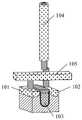
如图1A所示为平面晶体管的结构示意图,图1B为填埋式沟道晶体管的结构示意图。应当理解,图中为了使得各结构均能被清晰示出,可能造成各结构的尺寸比例关系与实际结构不符。其中,晶体管的源极101和漏极102分别位于栅极103的两侧,如此,在水平面上源极101和漏极102分别占用了不同的位置,使得不论是平面晶体管还是填埋式沟道晶体管的水平面积都较大。此外,由于电容104(Capacitor)和位线105(Bit Line,BL)在晶体管的同侧,在加工工艺中都位于衬底的一侧。以填埋式沟道晶体管为例,电容104的接触线需要穿过位线105,使得整体的工艺复杂度较高,对于光刻工艺和对准度有极高的要求。FIG. 1A is a schematic structural diagram of a planar transistor, and FIG. 1B is a structural schematic diagram of a buried channel transistor. It should be understood that in order to make each structure clearly shown in the drawings, the dimensional proportional relationship of each structure may be inconsistent with the actual structure. The
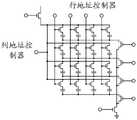
图1C为随机存取存储器中一个存储单元的示意图,图1D为随机存取存储器中存储单元阵列的示意图。其中,字线用于控制晶体管的通断,位线用于在晶体管导通时对电容进行读取和写入操作,电容的一端连接晶体管,另一端接地。1C is a schematic diagram of a memory cell in a random access memory, and FIG. 1D is a schematic diagram of a memory cell array in the random access memory. The word line is used to control the on-off of the transistor, and the bit line is used to read and write the capacitor when the transistor is on. One end of the capacitor is connected to the transistor, and the other end is grounded.
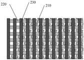
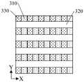
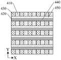
图1E为在一些实施例中存储单元阵列的晶体管的有源区的排布示意图。如图1E所示,有源区210的方向可以和位线呈18~25°夹角。1E is a schematic diagram of the arrangement of active regions of transistors of a memory cell array in some embodiments. As shown in FIG. 1E , the direction of the
图1F为在一些实施例中存储单元阵列的结构示意图。如图1F所示,字线220(WordLine,WL)和位线230互相垂直,每个有源区210与两条字线220和一条位线230相交。FIG. 1F is a schematic structural diagram of a memory cell array in some embodiments. As shown in FIG. 1F , word lines 220 (WordLine, WL) and
图1G为在一些实施例中存储单元阵列的局部结构示意图。如图1G所示,每个有源区210具有两个存储节点接触结构211(Storage Node Contact,SNC)和一个位线接触结构212(Bit Line Contact,BLC)。其中,两个存储节点接触结构211分别连接至两个电容,一个位线接触结构212连接至一条位线230。由此,单个位线230可以通过两条字线220的开关分别控制相邻的两个电容,从而进行读取和写入操作。从平面上看单位存储单元的尺寸为6F2(F为存储单元的最小外形尺寸,F2则表示单位面积),占用面积较大。FIG. 1G is a schematic diagram of a partial structure of a memory cell array in some embodiments. As shown in FIG. 1G , each
如图2所示,本申请实施例提供了一种存储器的制造方法,其对应的结构如图3A至图3F所示,所述制造方法包括以下步骤:As shown in FIG. 2 , an embodiment of the present application provides a method for manufacturing a memory, the corresponding structure of which is shown in FIGS. 3A to 3F , and the manufacturing method includes the following steps:
步骤S10、提供衬底300;Step S10, providing a
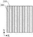
步骤S20、在所述衬底300中形成沿第一方向延伸的若干相互平行的第一隔离结构310;所述第一方向平行于所述衬底300表面;所述第一隔离结构310的第一厚度小于所述衬底300的厚度;Step S20 , forming a plurality of mutually parallel
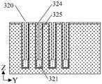
步骤S30、在所述衬底300中形成沿第二方向延伸的若干相互平行的第一沟槽320;所述第二方向平行于所述衬底300表面且与所述第一方向垂直;所述第一沟槽320与所述第一隔离结构310将所述衬底300划分为多个沟道柱330;Step S30, forming a plurality of mutually parallel
步骤S40、在所述第一沟槽320内形成字线结构340和第二隔离结构350;其中,所述字线结构340和所述第二隔离结构350并列排布,且沿所述第一沟槽320的侧壁延伸;Step S40, forming a
步骤S50、在所述字线结构340相邻的所述沟道柱330的表面形成存储结构360。Step S50 , forming a
在本申请实施例中,衬底300可以是硅(Si)、锗(Ge)等半导体材料。在一些实施例中,衬底300还可以是掺杂的,或者在衬底中包括掺杂区域和未掺杂区域。衬底300中用于形成第一沟槽320的一面可以作为衬底300的表面,与衬底300的表面相背的一面可以作为衬底300的背面。In this embodiment of the present application, the
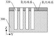
在本申请实施例中,如图3A所示,在衬底300的表面上形成沿第一方向延伸的若干第一隔离结构310。其中,第一方向平行于衬底表面,与Y方向一致;如图3B所示,第一隔离结构310在Z方向上的第一厚度小于衬底300的厚度。可选的,通过刻蚀(Etching)和/或光刻(Photolithography)工艺在衬底300的表面形成沿第一方向延伸的若干隔离槽;然后通过沉积工艺在隔离槽中形成第一隔离结构310。第一隔离结构310的材料包括但不限于二氧化硅(SiO2)、旋涂绝缘介质(Spin-on Dielectrics,SOD)、氮化硅(Si3N4)、氮氧化硅(SiON)。值得注意的是,本申请实施例中,对衬底的刻蚀是在Z方向进行的部分刻蚀,刻蚀过程不会将衬底刻穿。通常,刻蚀工艺可以分为干法刻蚀(Dry Etching)与湿法刻蚀(Wet Etching)。其中,干法刻蚀可以包括离子铣刻蚀(Ion Neam Milling Etching)、等离子体刻蚀(PlasmaEtching)、反应离子刻蚀(Reactive Ion Etching)或激光烧蚀(Laser Ablation)等;湿法刻蚀是利用溶剂或溶液来进行刻蚀,例如酸碱溶液。沉积工艺包括但不限于化学气相沉积(Chemical Vapor Deposition,CVD)、原子层沉积(Atomic Layer Deposition,ALD)或物理气相沉积(Physical Vapor Deposition,PVD)等。In this embodiment of the present application, as shown in FIG. 3A , a plurality of
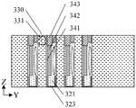
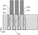
如图3C所示,在形成上述第一隔离结构310之后,可以通过刻蚀和/或光刻工艺在衬底300的表面上形成沿第二方向延伸的若干相互平行的第一沟槽320。其中,第二方向平行于衬底300表面,与X方向一致,与第一方向垂直。如图3D所示,第一沟槽320在Z方向上的深度小于衬底300的厚度。第一沟槽320与第一隔离结构310将衬底300划分为多个沟道柱330。沟道柱330的长度方向与Z方向一致,从而使得沟道柱330靠近衬底300表面和背面的两端,可以分别形成存储器中晶体管的源极和漏极,即存储器中的晶体管的方向垂直于衬底表面。由此,垂直的晶体管占用面积更小,故单位面积上存储单元的密度更大。As shown in FIG. 3C , after the above-mentioned
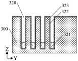
如图3E所示,在第一沟槽320内形成字线结构340和第二隔离结构350。其中,字线结构340与第二隔离结构350在Y方向上并列排布,并在X方向上沿着第一沟槽320的侧壁延伸。字线结构340和第二隔离结构350分别覆盖第一沟槽320相对的两个侧壁,第二隔离结构350用于电隔离字线结构340和相邻晶体管中的沟道柱330。可选的,可以在第一沟槽320内分别形成字线结构340和第二隔离结构350对应的牺牲层,然后依次对牺牲层进行替换,形成字线结构340与第二隔离结构350。字线结构340可以包括字线、栅氧化层、栅保护层等结构,其中字线为导电材料,包括但不限于钨(W)、氮化钛(TiN)、铜(Cu)、银(Ag)中的一种或多种。第二隔离结构350的材料包括但不限于二氧化硅、旋涂绝缘介质、氮化硅、氮氧化硅中的一种或多种。As shown in FIG. 3E ,
如图3F所示,在字线结构340相邻的沟道柱330的表面形成存储结构360。沟道柱330的方向与Z方向一致,故可以在沟道柱330的两端,分别形成晶体管的源极和漏极,即存储器中的晶体管的方向垂直于衬底表面。存储结构360可以形成在沟道柱330任意一端的表面上,与晶体管的源极或漏极连接,沟道柱330的另一端则可以用于形成位线等结构。在随机存取存储器中,存储结构360可以是电容。由此,存储器中源极和漏极所连接的不同结构可以分别设计在衬底300相对的两个面上,从而简化了存储器内部的电路布局,降低了存储器制造的工艺难度。As shown in FIG. 3F , a
在一些实施例中,如图3G所示,在形成所述第一沟槽320之前,还可以在衬底300的表面上通过沉积工艺依次形成一层氧化硅层和一层氮化硅层,以在后续的工艺中保护衬底300的表面。In some embodiments, as shown in FIG. 3G, before forming the
在一些实施例中,如图4所示,所述方法还包括:In some embodiments, as shown in FIG. 4 , the method further includes:
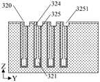
在所述第一沟槽320底部形成第二厚度的第三隔离结构321;所述第二厚度小于所述第一沟槽320的深度;所述字线结构340和所述第二隔离结构350形成于所述第三隔离结构321上方。A
在本申请实施例中,可以通过沉积等工艺在第一沟槽320的底部形成第三隔离结构321,第三隔离结构321在Z方向上的厚度小于第一沟槽320的深度。字线结构340和第二隔离结构350形成于第三隔离结构321的上方,第三隔离结构321用于防止字线结构340在第一沟槽320的底部发生漏电流现象。第三隔离结构321的材料包括但不限于二氧化硅、旋涂绝缘介质、氮化硅、氮氧化硅中的一种或多种。In this embodiment of the present application, the
在一些实施例中,如图5所示,所述方法还包括:In some embodiments, as shown in Figure 5, the method further includes:
形成覆盖所述第一沟槽320内壁的第一氧化层322;forming a
形成覆盖所述第一氧化层322的第一保护层323;forming a first
所述在所述第一沟槽320底部形成第二厚度的第三隔离结构321,包括:The forming the
在内壁覆盖有所述第一氧化层322和所述第一保护层323的所述第一沟槽320内,形成所述第三隔离结构321。The
在本申请实施例中,可以通过沉积工艺在第一沟槽320的内壁上形成第一氧化层322,这里的内壁包括第一沟槽320的侧壁和底面,第一氧化层322可以为线形氧化层(LinerOxide),第一氧化层322可以在后续工艺中保护第一沟槽320的内壁。然后,利用沉积工艺形成覆盖在第一氧化层322上的第一保护层323,第一保护层323可以为氮化硅等材料,第一保护层323可以作为后续从背面减薄衬底300的停止层。示例性地,采用原子层沉积的方法在第一沟槽320中依次形成第一氧化层322和第一保护层323,然后在内壁覆盖有第一氧化层322和第一保护层323的第一沟槽320的底部,形成具有第二厚度的第三隔离结构321,第二厚度小于第一沟槽320的深度。In this embodiment of the present application, the
在一些实施例中,如图6A-图6C所示,所述在内壁覆盖有所述第一氧化层322和所述第一保护层323的所述第一沟槽320内,形成所述第三隔离结构321,包括:In some embodiments, as shown in FIGS. 6A-6C , in the
在内壁覆盖有所述第一氧化层322和所述第一保护层323的所述第一沟槽320内,填充绝缘材料;Fill insulating material in the
去除至少部分所述绝缘材料,使所述第一沟槽320底部保留所述第二厚度的所述绝缘材料以形成所述第三隔离结构321;removing at least part of the insulating material so that the insulating material of the second thickness remains at the bottom of the
去除所述第三隔离结构321上方的所述第一保护层323。The first
在本申请实施例中,如图6A所示,可以通过旋涂绝缘介质工艺,在内壁覆盖有第一氧化层322和第一保护层323的第一沟槽320内,填充绝缘材料,这里的绝缘材料可以为二氧化硅等,当然,也可以使用其他合适的工艺。如图6B所示,可以利用刻蚀等工艺,去除部分上述绝缘材料,使第一沟槽320的底部保留第二厚度的绝缘材料,从而形成第三隔离结构321。如图6C所示,可以通过选择性刻蚀,去除位于第三隔离结构321上方的第一保护层323。由于后续工艺会在第三隔离结构321上方形成字线结构340,且第一保护层323仅作为从背面减薄衬底300的停止层,相应地,可以去除第三隔离结构321上方的第一保护层323。示例性地,采用磷酸(H3PO4)、氢氟酸(HF)等选择性刻蚀溶液,可以去除氮化硅材料的第一保护层323,而不与第一氧化层322以及第三隔离结构321中的二氧化硅材料发生反应。In this embodiment of the present application, as shown in FIG. 6A , an insulating material may be filled in the
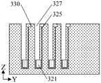
在一些实施例中,如图7所示,所述在所述第一沟槽320内形成字线结构340和第二隔离结构350,包括以下步骤,其对应的结构如图8A至图8F所示:In some embodiments, as shown in FIG. 7 , the forming of the
步骤S401:在所述第一沟槽320底部,形成所述第三隔离结构321;Step S401 : forming the
步骤S402:在所述第三隔离结构321上方,形成覆盖所述第一沟槽320的第一侧壁的第一牺牲层324,并形成覆盖所述第一沟槽320的第二侧壁的第二牺牲层325;其中,所述第一侧壁和所述第二侧壁为所述第一沟槽320内相对的不同侧壁;Step S402 : above the
步骤S403:在所述第一牺牲层324和所述第二牺牲层325之间形成间隔层326;Step S403: forming a
步骤S404:去除所述第一牺牲层324,形成第二沟槽327;Step S404: removing the first
步骤S405:在所述第二沟槽327中形成所述字线结构340;Step S405 : forming the
步骤S406:去除所述第二牺牲层325,形成第三沟槽328;Step S406: removing the second
步骤S407:在所述第三沟槽328中形成所述第二隔离结构350。Step S407 : forming the
在本申请实施例中,如图8A所示,可以通过原子层沉积工艺,在第三隔离结构321上方形成第一牺牲层324和第二牺牲层325,第一牺牲层324和第二牺牲层325可以为多晶硅(Polycrystalline Silicon,Poly-Si)材料。其中,第一牺牲层324覆盖于第一沟槽320的第一侧壁上,第二牺牲层325覆盖于第一沟槽320的第二侧壁上,第一侧壁与第二侧壁为第一沟槽320在Y方向上相对的两个侧壁。第一牺牲层324和第二牺牲层325相互分离,且第一牺牲层324和第二牺牲层325之间具有空隙。第一牺牲层324和第二牺牲层325用于形成在第一沟槽320内并列排布,且沿X方向延伸的字线结构340和第二隔离结构350。In this embodiment of the present application, as shown in FIG. 8A , the first
如图8B所示,可以通过沉积等工艺,在第一牺牲层324和第二牺牲层325之间的空隙中形成间隔层326,间隔层326可以为二氧化硅等材料,用于在后续去除第一牺牲层324和形成字线结构340的过程中,保护第二牺牲层325。As shown in FIG. 8B , a
如图8C所示,可以通过刻蚀等工艺,去除第一牺牲层324,形成第二沟槽327,第二沟槽327用于形成字线结构340。As shown in FIG. 8C , the first
如图8D所示,可以通过沉积等工艺,在第二沟槽327中形成字线结构340。字线结构340可以包括字线、栅氧化层、栅保护层等结构,其中字线为导电材料,包括但不限于钨(W)、氮化钛(TiN)、铜(Cu)、银(Ag)中的一种或多种。As shown in FIG. 8D , the
如图8E所示,可以通过刻蚀等工艺,去除第二牺牲层325,形成第三沟槽328,第三沟槽328用于形成第二隔离结构350。As shown in FIG. 8E , the second
如图8F所示,可以通过沉积等工艺,在第三沟槽328中形成第二隔离结构350。第二隔离结构350用于电隔离字线结构340和相邻晶体管中的沟道柱330。第二隔离结构350的材料包括但不限于二氧化硅、旋涂绝缘介质、氮化硅、氮氧化硅中的一种或多种。As shown in FIG. 8F , the
在一些实施例中,如图9A和图9B所示,所述形成覆盖所述第一沟槽320的第一侧壁的第一牺牲层324,并形成覆盖所述第一沟槽320的第二侧壁的第二牺牲层325,包括:In some embodiments, as shown in FIGS. 9A and 9B , the first
在所述第一沟槽320内形成覆盖所述第一沟槽320内壁的牺牲层329;forming a
去除所述第三隔离结构321上表面的部分所述牺牲层329,形成相互分离的所述第一牺牲层324和所述第二牺牲层325。Part of the
在本申请实施例中,如图9A所示,可以通过沉积等工艺,形成覆盖第一沟槽320内壁,并沿X方向延伸的牺牲层329。这里的内壁包括第一沟槽320的第一侧壁、第二侧壁和第三隔离结构321的上表面,牺牲层329可以为多晶硅材料。In the embodiment of the present application, as shown in FIG. 9A , a
如图9B所示,可以通过干法刻蚀工艺,去除第三隔离结构321上表面的部分所述牺牲层329,使得位于第一侧壁、第二侧壁的牺牲层329相互分离,从而形成第一牺牲层324和第二牺牲层325。第一牺牲层324和第二牺牲层325用于形成在第一沟槽320内并列排布,且沿X方向延伸的字线结构340和第二隔离结构350。As shown in FIG. 9B , a part of the
在一些实施例中,如图10A-图10D所示,所述去除所述第一牺牲层324,形成第二沟槽327,包括:In some embodiments, as shown in FIGS. 10A-10D , the removing the first
在所述第二牺牲层325靠近所述衬底300表面的一端上形成第四沟槽3251;forming a
在所述第四沟槽3251中形成覆盖所述第二牺牲层325的第二保护层3252;forming a second
去除所述第一牺牲层324,形成所述第二沟槽327。The first
在本申请实施例中,如图10A所示,可以通过刻蚀和/或光刻工艺在第二牺牲层325靠近衬底300的一端上形成第四沟槽3251,第四沟槽3251用于形成第二保护层3252,且第四沟槽3251在XY平面上的投影完全覆盖第二牺牲层325。In this embodiment of the present application, as shown in FIG. 10A , a
如图10B所示,可以通过沉积等工艺,在第四沟槽3251中形成覆盖所述第二牺牲层325的第二保护层3252,第二保护层3252可以为二氧化硅等材料。第二保护层3252和间隔层326将第一牺牲层324和第二牺牲层325完全分隔开,从而在后续去除第一牺牲层324和形成字线结构340的过程中,保护第二牺牲层325。As shown in FIG. 10B , a second
需要说明的是,由于第四沟槽3251与衬底300表面存在高度差,故在沉积形成第二保护层3252后,如图10C所示,第二保护层3252和衬底300的表面会存在不平整的现象,影响后续工艺。可选的,在沉积形成第二保护层3252后,可以对衬底300的表面进行平坦化处理,例如化学机械抛光(Chemical Mechanical Polishing,CMP),来去除多余的半导体材料。It should be noted that, due to the height difference between the
如图10D所示,可以通过刻蚀等工艺,去除第一牺牲层324,形成第二沟槽327,第二沟槽327用于形成字线结构340。As shown in FIG. 10D , the first
在一些实施例中,如图11A-图11E所示,所述在所述第二沟槽327中形成所述字线结构340,包括:In some embodiments, as shown in FIGS. 11A-11E , the forming the
去除所述间隔层326和所述第二沟槽327中的第一氧化层322;removing the
在所述第二沟槽327的侧壁形成栅氧化层341;A
在所述第二沟槽327中填充导电材料;filling the
去除至少部分所述导电材料,形成具有第三厚度的字线342,所述第三厚度小于所述第二沟槽327的深度;removing at least part of the conductive material to form
在所述第二沟槽327中的所述字线342上填充绝缘材料,形成栅保护层343;其中所述字线结构340包括所述栅氧化层341、所述字线342和所述栅保护层343。An insulating material is filled on the
在本申请实施例中,如图11A所示,为了在第二沟槽327的侧壁形成目标厚度且质量较好的栅氧化层,可以通过刻蚀等工艺,去除间隔层326和第二沟槽327中位于第三隔离结构321上方的部分第一氧化层322,从而暴露出相邻的沟道柱330和第二牺牲层325,以便于在第二沟槽327的侧壁上进行氧化处理形成栅氧化层。可选的,在去除间隔层326和部分第一氧化层322后,利用湿法清洗工艺,以去除第二沟槽327内部残留的污染物。In this embodiment of the present application, as shown in FIG. 11A , in order to form a gate oxide layer with a target thickness and better quality on the sidewall of the
如图11B所示,可以通过热氧化工艺,在第二沟槽327的侧壁形成目标厚度的栅氧化层341,热氧化工艺可以为蒸汽原位生成(In-Situ Steam Generated,ISSG)、快速热氧化工艺(Rapid Thermal Oxidation,RTO)等。值得注意的是,这里的栅氧化层341位于第二沟槽327中靠近相邻沟道柱330的侧壁上。而位于第二沟槽327中靠近第二牺牲层325的侧壁上的氧化层,则用于在后续去除第二牺牲层325的过程中,保护字线结构340。As shown in FIG. 11B , a
如图11C所示,可以通过沉积等工艺,在具有栅氧化层341的第二沟槽327中填充导电材料,以形成字线。其中,导电材料包括但不限于钨、氮化钛、铜、银中的一种或多种。As shown in FIG. 11C , a conductive material may be filled in the
如图11D所示,可以通过刻蚀等工艺,去除至少部分导电材料,以形成第三厚度的字线342,字线342的第三厚度小于第二沟槽327的深度,便于继续在字线342的上方形成栅保护层。As shown in FIG. 11D , at least part of the conductive material may be removed through processes such as etching to form
如图11E所示,可以通过沉积等工艺,在字线342的上方填充绝缘材料,形成栅保护层343。可选的,这里的绝缘材料可以为氮化硅。栅保护层343可以防止字线342在靠近衬底300表面的一端发生漏电流现象,并在后续的工艺中保护字线342。As shown in FIG. 11E , an insulating material may be filled over the word lines 342 through a process such as deposition to form a
字线结构340包括上述栅氧化层341、字线342和栅保护层343。The
在一些实施例中,如图12A和图12B所示,所述去除所述第二牺牲层325,形成第三沟槽328,包括:In some embodiments, as shown in FIG. 12A and FIG. 12B , the removing the second
去除所述第二保护层3252;removing the second
去除所述第二牺牲层325,形成所述第三沟槽328。The second
在本申请实施例中,如图12A所示,可以通过化学机械抛光等工艺,对衬底300表面进行处理,以去除第二保护层3252,和形成字线结构340后残留在衬底300表面的多余半导体材料,从而暴露出第二牺牲层325位于衬底300表面的一端,形成去除第二牺牲层325的开口。In this embodiment of the present application, as shown in FIG. 12A , the surface of the
如图12B所示,可以通过刻蚀等工艺,去除第二牺牲层325,形成第三沟槽328。第三沟槽328用于形成第二隔离结构350。As shown in FIG. 12B , the second
在一些实施例中,如图13所示,所述在所述第三沟槽328中形成所述第二隔离结构350,包括:In some embodiments, as shown in FIG. 13 , forming the
在所述第三沟槽328中填充绝缘材料,形成中间具有空气间隙351(Air Gap)的所述第二隔离结构350。An insulating material is filled in the
在本申请实施例中,如图13所示,可以通过沉积等工艺,在第三沟槽328中填充绝缘材料,并利用刻蚀等工艺,形成中间具有空气间隙351的第二隔离结构350。其中,空气间隙351在Z方向上的长度大于等于字线342的第三厚度。可选的,这里的绝缘材料可以为二氧化硅。空气间隙351可以提高第二隔离结构350的介电性能,进而改善半导体器件的性能。In this embodiment of the present application, as shown in FIG. 13 , the
在一些实施例中,如图14A和图14B所示,所述形成中间具有空气间隙351的所述第二隔离结构350之后,还包括:In some embodiments, as shown in FIG. 14A and FIG. 14B , after forming the
在所述第二隔离结构350靠近所述衬底300表面的一端形成第五沟槽352;A
在所述第五沟槽352中填充绝缘材料,形成第三保护层353。An insulating material is filled in the
在本申请实施例中,如图14A所示,可以通过刻蚀等方法,在第二隔离结构350靠近衬底300表面的一端形成第五沟槽352。其中,第五沟槽352不与空气间隙351连通,第五沟槽352用于形成第三保护层353。In this embodiment of the present application, as shown in FIG. 14A , a
如图14B所示,可以通过沉积等方法,在第五沟槽352中填充绝缘材料,形成第三保护层353。这里的绝缘材料可以为氮化硅等材料。第三保护层353可以保护空气间隙351,并提高第二隔离结构350的介电性能。由于在形成第三保护层353之后,衬底300的表面会存在不平整的现象,可选的,通过化学机械抛光工艺,对衬底300表面进行平坦化处理。As shown in FIG. 14B , an insulating material may be filled in the
在一些实施例中,如图15所示,所述方法还包括:In some embodiments, as shown in Figure 15, the method further includes:
对所述沟道柱330的第一端进行掺杂,形成晶体管的源极331;Doping the first end of the
对所述沟道柱330的第二端进行掺杂,形成所述晶体管的漏极332。Doping the second end of the
在本申请实施例中,如图15所示,可以通过离子注入(Implant)工艺,对沟道柱330的第一端和第二端进行掺杂,形成晶体管的源极331和漏极332。其中,第一端和第二端为沟道柱330在Z方向上相对的两端。可以理解的是,第一端可以为沟道柱330靠近衬底300表面的一端,也可以为沟道柱330靠近衬底300背面的一端。In this embodiment of the present application, as shown in FIG. 15 , the first end and the second end of the
在一些实施例中,由于衬底300的表面存在氧化硅层、氮化硅层等残留材料,在形成晶体管的源极331和/或漏极332后,需要通过刻蚀、化学机械抛光等工艺去除残留物,以暴露出源极331和/或漏极332。In some embodiments, since residual materials such as a silicon oxide layer and a silicon nitride layer exist on the surface of the
在一些实施例中,如图16所示,所述在所述字线结构340相邻的所述沟道柱330的表面形成存储结构360,包括:In some embodiments, as shown in FIG. 16 , forming a
在所述字线结构340相邻的所述源极331的表面上形成存储电容361。A
在本申请实施例中,如图16所示,字线结构340相邻的源极331是指靠近栅氧化层341一侧的沟道柱330中的源极331。可以理解的是,存储电容361既可以形成在源极331的表面上,也可以形成在漏极332的表面上。存储电容361的一端与源极331或者漏极332连接,另一端接地。In the embodiment of the present application, as shown in FIG. 16 , the
在一些实施例中,如图17A和图17B所示,所述对所述沟道柱330的第二端进行掺杂,形成所述晶体管的漏极332,包括:In some embodiments, as shown in FIGS. 17A and 17B , doping the second end of the
对所述衬底300的背面进行减薄,直至暴露所述第三隔离结构321;thinning the backside of the
对所述第三隔离结构321相邻的所述沟道柱330的第二端进行掺杂,形成所述晶体管的漏极332。Doping the second end of the
在本申请实施例中,如图17A所示,利用化学机械抛光等工艺对衬底300的背面进行减薄,直至暴露第三隔离结构321底部的第一保护层323,第一保护层323可以作为化学机械抛光工艺的停止层。In this embodiment of the present application, as shown in FIG. 17A , the backside of the
如图17B所示,通过离子注入(Implant)工艺,对第三隔离结构321相邻的沟道柱330的第二端进行掺杂,形成晶体管的漏极332,这里的第二端指的是沟道柱330靠近衬底300背面的一端。可以理解的是,也可以在沟道柱330靠近衬底300背面的一端形成晶体管的源极331。As shown in FIG. 17B , the second end of the
在一些实施例中,如图18所示,所述方法还包括:In some embodiments, as shown in Figure 18, the method further includes:
在所述衬底300的背面,形成连接所述晶体管的漏极332的位线370。On the backside of the
在本申请实施例中,如图18所示,在衬底300的背面,形成连接晶体管的漏极332的位线370,位线370为导电材料。当字线342控制源极331和漏极332之间导通时,位线370对存储电容361进行数据的读取和写入操作。可以理解的是,位线370与存储电容361分别形成于衬底300相对的两个面上,从而简化了存储器内部的电路布局,降低了存储器制造的工艺难度。In this embodiment of the present application, as shown in FIG. 18 , on the backside of the
在一些实施例中,如图19所示,所述在所述衬底300的背面,形成连接所述晶体管的漏极332的位线370,包括:In some embodiments, as shown in FIG. 19 , forming a
在所述漏极332表面形成位线接触结构371;forming a bit
在所述位线接触结构371上形成所述位线370。The
在本申请实施例中,如图19所示,在漏极332表面形成位线接触结构371,并在位线接触结构371上形成位线370。位线接触结构371为导电材料,用于连接漏极332和位线370。In this embodiment of the present application, as shown in FIG. 19 , a bit
如图20A和图20B所示,本申请实施例还提供了一种存储器40,所述存储器40包括:As shown in FIG. 20A and FIG. 20B , an embodiment of the present application further provides a memory 40, where the memory 40 includes:
衬底400;
位于所述衬底400中且沿第一方向延伸的若干相互平行的第一隔离结构410;所述第一方向平行于所述衬底400表面;所述第一隔离结构410的第一厚度小于或等于所述衬底400的厚度;A plurality of mutually parallel
位于所述衬底400中且沿第二方向延伸的若干相互平行的第一沟槽420;所述第二方向平行于所述衬底400表面且与所述第一方向垂直;所述第一沟槽420与所述第一隔离结构410将所述衬底划分为多个沟道柱430;A plurality of mutually parallel
位于所述第一沟槽420内的字线结构440和第二隔离结构450;其中,所述字线结构440和所述第二隔离结构450并列排布,且沿所述第一沟槽420的侧壁延伸;The
位于所述字线结构440相邻的所述沟道柱430的表面的存储结构460。The
在本申请实施例中,衬底400可以是硅(Si)、锗(Ge)等半导体材料。在一些实施例中,衬底400还可以是掺杂的,或者在衬底400中包括掺杂区域和未掺杂区域。衬底400中第一沟槽420所在的一面可以作为衬底400的表面,与衬底400的表面相背的一面可以作为衬底400的背面。In this embodiment of the present application, the
如图20A所示,第一隔离结构410位于衬底400的表面,且沿着第一方向延伸。其中,第一方向平行于衬底400表面,与Y方向一致。第一隔离结构410在Z方向上的第一厚度小于或等于衬底400的厚度。图20A中未示出存储结构460。As shown in FIG. 20A , the
如图20A所示,第一沟槽420位于衬底400的表面,且沿着第二方向延伸。其中,第二方向平行于衬底400表面,与X方向一致,与第一方向垂直。如图20B所示,第一沟槽420在Z方向上的深度小于或等于衬底400的厚度。第一沟槽420与第一隔离结构410将衬底400划分为多个沟道柱430。沟道柱430的长度方向与Z方向一致,从而使得沟道柱430靠近衬底400表面和背面的两端,可以分别形成存储器中晶体管的源极和漏极,即存储器中的晶体管的方向垂直于衬底400表面。由此,垂直的晶体管占用面积更小,故单位面积上存储单元的密度更大。As shown in FIG. 20A , the
如图20A所示,字线结构440与第二隔离结构450在Y方向上并列排布,并在X方向上沿着第一沟槽420的侧壁延伸。如图20B所示,字线结构440和第二隔离结构450分别覆盖第一沟槽420相对的两个侧壁,第二隔离结构450用于电隔离字线结构440和相邻晶体管中的沟道柱430。字线结构440可以包括字线、栅氧化层、栅保护层等结构,其中字线为导电材料,包括但不限于钨(W)、氮化钛(TiN)、铜(Cu)、银(Ag)中的一种或多种。第二隔离结构450的材料包括但不限于二氧化硅、旋涂绝缘介质、氮化硅、氮氧化硅中的一种或多种。As shown in FIG. 20A , the
如图20B所示,存储结构460位于字线结构440相邻的沟道柱430的表面。可以理解的是,存储结构460可以位于沟道柱430任意一端的表面上,与晶体管的源极或漏极连接,沟道柱430的另一端则可以连接位线等结构。在随机存取存储器中,存储结构460可以是电容。由此,存储器中源极和漏极所连接的不同结构可以分别设计在衬底400相对的两个面上,从而简化了存储器内部的电路布局,降低了存储器制造的工艺难度。As shown in FIG. 20B , the
在一些实施例中,如图21所示,所述存储器还包括:In some embodiments, as shown in Figure 21, the memory further includes:
位于所述第一沟槽420底部的具有第二厚度的第三隔离结构421;所述第二厚度小于所述第一沟槽420的深度;所述字线结构440和所述第二隔离结构450位于所述第三隔离结构421上方。A
在本申请实施例中,第三隔离结构421位于第一沟槽420的底部,第三隔离结构421在Z方向上的厚度小于第一沟槽420的深度。字线结构440和第二隔离结构450位于第三隔离结构421的上方,第三隔离结构421用于防止字线结构440在第一沟槽420的底部发生漏电流现象。第三隔离结构421的材料包括但不限于二氧化硅、旋涂绝缘介质、氮化硅、氮氧化硅中的一种或多种。In the embodiment of the present application, the
在一些实施例中,如图22所示,所述存储器还包括:In some embodiments, as shown in Figure 22, the memory further includes:
第一保护层423,位于所述第三隔离结构421和所述第一沟槽420的内壁之间;a first
第一氧化层422,位于所述第一保护层423和所述第一沟槽420的内壁之间。The
在本申请实施例中,第一保护层423位于第三隔离结构421和第一沟槽420的内壁之间,第一保护层423可以为氮化硅等材料;第一氧化层422位于第一保护层423和第一沟槽420的内壁之间,第一氧化层422可以为线形氧化层。第一保护层423和第一氧化层422可以提高第三隔离结构421的介电性能,防止字线结构440在第一沟槽420的底部发生漏电流现象。In the embodiment of the present application, the first
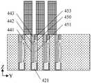
在一些实施例中,如图23所示,所述字线结构440包括:In some embodiments, as shown in FIG. 23, the
字线442,位于所述第三隔离结构421上方;word lines 442 located above the
栅氧化层441,位于所述字线442和相邻的所述沟道柱430之间;The
栅保护层443,位于所述字线442上方。The
在本申请实施例中,字线结构440包括:字线442、栅氧化层441和栅保护层443。其中,字线442位于第三隔离结构421上方,字线442的顶端低于衬底400表面,字线442为导电材料,包括但不限于钨、氮化钛、铜、银中的一种或多种。In the embodiment of the present application, the
栅氧化层441位于字线442和相邻的沟道柱430之间,栅氧化层441可以通过对第一沟槽420的侧壁进行热氧化工艺形成。The
栅保护层443覆盖于字线442上方,栅保护层443可以为氮化硅材料,用于防止字线442在靠近衬底400表面的一端发生漏电流现象。The
在一些实施例中,如图24所示,所述第二隔离结构450中具有空气间隙451。In some embodiments, as shown in FIG. 24 , the
在本申请实施例中,第二隔离结构450中具有空气间隙451。其中,第二隔离结构450可以为二氧化硅等绝缘材料;空气间隙451在Z方向上的长度大于等于字线442在Z方向上的长度,空气间隙451可以提高第二隔离结构450的介电性能,进而改善半导体器件的性能。In the embodiment of the present application, the
在一些实施例中,如图25所示,所述第二隔离结构450还包括:In some embodiments, as shown in FIG. 25 , the
第三保护层453,位于空气间隙451上方。The third
在本申请实施例中,第三保护层453位于空气间隙451上方,第三保护层453可以为氮化硅等绝缘材料,用于保护空气间隙451,并提高第二隔离结构450的介电性能。In the embodiment of the present application, the third
在一些实施例中,如图26所示,所述沟道柱430包括:In some embodiments, as shown in FIG. 26 , the
位于所述沟道柱430第一端的晶体管的源极431;the
位于所述沟道柱430第二端的所述晶体管的漏极432。The
在本申请实施例中,晶体管的源极431和漏极432分别位于沟道柱430在Z方向上相对的两端。可以理解的是,晶体管的源极431既可以位于沟道柱430靠近衬底400表面的一端,也可以为沟道柱430靠近衬底400背面的一端。In the embodiment of the present application, the
在一些实施例中,如图27所示,所述存储结构460包括:In some embodiments, as shown in FIG. 27, the
存储电容461,位于所述源极431的表面且连接所述源极431。The
在本申请实施例中,存储电容461位于源极431的表面且连接所述源极431,用于存储写入的数据。可以理解的是,存储电容461既可以位于源极431的表面上,也可以位于漏极432的表面上。存储电容461的一端与源极431或者漏极432连接,另一端接地。In the embodiment of the present application, the
在一些实施例中,如图28A至图28C所示,所述存储电容461包括但不限于:杯形(Cup-Type)电容、筒形(Cylinder-Type)电容、柱形(Pillar-Type)电容。In some embodiments, as shown in FIGS. 28A to 28C , the
在本申请实施例中,如图28A所示为杯形电容的结构示意图,其中下电极4611为向上开口的杯形,上电极4612位于下电极4611的内侧。In the embodiment of the present application, FIG. 28A is a schematic structural diagram of a cup-shaped capacitor, wherein the
如图28B所示为筒形电容的结构示意图,其中下电极4611为向上开口的杯形;上电极4612包围下电极4611的内侧和外侧。28B is a schematic structural diagram of a cylindrical capacitor, wherein the
如图28C所示为柱形电容的结构示意图,其中下电极4611为柱形,上电极4612包围下电极4611且向下开口。FIG. 28C is a schematic structural diagram of a columnar capacitor, wherein the
上电极4612和下电极4611均为导电材料,包括金属和金属氮化物材料,如钨、镍、钽、氮化钽和氮化钛中的一种或多种;电容介质层4613为高K介电材料,如氧化钛、氧化锆、氧化铪等。The
在一些实施例中,如图29A和图29B所示,所述存储电容461在衬底400表面上的排布包括但不限于:正方形排布、六边形排布。In some embodiments, as shown in FIGS. 29A and 29B , the arrangement of the
在本申请实施例中,如图29A所示为存储电容461在衬底400表面上呈正方形排布的示意图,各个存储电容461在X和Y方向上的间距可以与各个沟道柱430的间距相等。存储电容461在XY平面上的中心可以相对沟道柱430的中心有一定的偏移。In this embodiment of the present application, as shown in FIG. 29A , a schematic diagram of the
如图29B所示为存储电容461在衬底400表面上呈六边形排布的示意图,相邻的两行存储电容461可以沿X方向错位排布。FIG. 29B is a schematic diagram showing that the
在一些实施例中,存储电容461在Z方向上的截面形状可以为椭圆形,且存储电容461的椭圆截面的轴线与X方向不平行,以减小电容占用的面积。In some embodiments, the cross-sectional shape of the
在一些实施例中,如图30所示,所述存储器还包括:In some embodiments, as shown in Figure 30, the memory further includes:
位线470,位于所述衬底400的背面,所述位线470连接所述漏极432。A
在本申请实施例中,位线470位于衬底400的背面,且连接至漏极432,位线470为导电材料。当字线442控制源极431和漏极432之间导通时,位线470对存储电容461进行数据的读取和写入操作。可以理解的是,位线470与存储电容461分别形成于衬底400相对的两个面上,从而简化了存储器内部的电路布局,降低了存储器制造的工艺难度。In the embodiment of the present application, the
在一些实施例中,如图31所示,所述存储器还包括:In some embodiments, as shown in Figure 31, the memory further includes:
位线接触结构471,位于所述漏极432的表面,所述位线接触结构471连接所述漏极432和所述位线470。The bit
在本申请实施例中,位线接触结构471位于漏极432的表面,位线接触结构471为导电材料,且连接位线470和漏极432。In the embodiment of the present application, the bit
需要说明的是,本申请所提供的实施例,可以应用于随机存取存储器(RAM)、动态随机存取存储器(DRAM)、铁电随机存取存储器(FRAM)、相变随机存取存储器(PCRAM)、磁性随机存取存储器(MRAM)等。It should be noted that the embodiments provided in this application can be applied to random access memory (RAM), dynamic random access memory (DRAM), ferroelectric random access memory (FRAM), phase change random access memory ( PCRAM), Magnetic Random Access Memory (MRAM), etc.
需要说明的是,本申请所提供的几个方法或设备实施例中所揭露的特征,在不冲突的情况下可以任意组合,得到新的方法实施例或设备实施例。It should be noted that, the features disclosed in several method or device embodiments provided in this application may be combined arbitrarily under the condition of no conflict to obtain new method embodiments or device embodiments.
以上所述,仅为本申请的具体实施方式,但本申请的保护范围并不局限于此,任何熟悉本技术领域的技术人员在本申请揭露的技术范围内,可轻易想到变化或替换,都应涵盖在本申请的保护范围之内。因此,本申请的保护范围应以所述权利要求的保护范围为准。The above are only specific embodiments of the present application, but the protection scope of the present application is not limited to this. should be covered within the scope of protection of this application. Therefore, the protection scope of the present application should be subject to the protection scope of the claims.
Claims (24)
Priority Applications (1)
| Application Number | Priority Date | Filing Date | Title |
|---|---|---|---|
| CN202210160600.9ACN114220765B (en) | 2022-02-22 | 2022-02-22 | Memory and method of making the same |
Applications Claiming Priority (1)
| Application Number | Priority Date | Filing Date | Title |
|---|---|---|---|
| CN202210160600.9ACN114220765B (en) | 2022-02-22 | 2022-02-22 | Memory and method of making the same |
Publications (2)
| Publication Number | Publication Date |
|---|---|
| CN114220765A CN114220765A (en) | 2022-03-22 |
| CN114220765Btrue CN114220765B (en) | 2022-06-21 |
Family
ID=80709246
Family Applications (1)
| Application Number | Title | Priority Date | Filing Date |
|---|---|---|---|
| CN202210160600.9AActiveCN114220765B (en) | 2022-02-22 | 2022-02-22 | Memory and method of making the same |
Country Status (1)
| Country | Link |
|---|---|
| CN (1) | CN114220765B (en) |
Families Citing this family (2)
| Publication number | Priority date | Publication date | Assignee | Title |
|---|---|---|---|---|
| CN114530420B (en)* | 2022-04-24 | 2022-08-05 | 芯盟科技有限公司 | Semiconductor structure and manufacturing method thereof |
| CN117219612A (en)* | 2022-05-30 | 2023-12-12 | 长鑫存储技术有限公司 | Method for manufacturing semiconductor structure and memory |
Family Cites Families (12)
| Publication number | Priority date | Publication date | Assignee | Title |
|---|---|---|---|---|
| US7229895B2 (en)* | 2005-01-14 | 2007-06-12 | Micron Technology, Inc | Memory array buried digit line |
| US8872247B2 (en)* | 2009-11-04 | 2014-10-28 | Micron Technology, Inc. | Memory cells having a folded digit line architecture |
| KR20130005120A (en)* | 2011-07-05 | 2013-01-15 | 에스케이하이닉스 주식회사 | Method for manufacturing semiconductor device with vertical gate |
| KR20130103942A (en)* | 2012-03-12 | 2013-09-25 | 에스케이하이닉스 주식회사 | Semiconductor device having junctionless vertical gate transistor and method for manufacturing the same |
| US8987796B2 (en)* | 2012-08-17 | 2015-03-24 | Ps4 Luxco S.A.R.L. | Semiconductor device having semiconductor pillar |
| KR101927717B1 (en)* | 2012-08-30 | 2018-12-11 | 삼성전자주식회사 | Semiconductor device and method of forming the same |
| KR102657070B1 (en)* | 2019-01-03 | 2024-04-16 | 삼성전자주식회사 | Semiconductor device and method of forming the same |
| CN113437068B (en)* | 2021-06-24 | 2022-04-19 | 芯盟科技有限公司 | Dynamic random access memory and forming method thereof |
| CN113629054B (en)* | 2021-07-02 | 2024-10-25 | 芯盟科技有限公司 | U-shaped transistor array and forming method thereof, semiconductor device and forming method thereof |
| CN113488468A (en)* | 2021-07-07 | 2021-10-08 | 芯盟科技有限公司 | Semiconductor structure and method for forming semiconductor structure |
| CN113517292B (en)* | 2021-07-08 | 2024-12-10 | 芯盟科技有限公司 | Semiconductor structure and method for forming the same |
| CN113707660B (en)* | 2021-09-02 | 2024-04-05 | 芯盟科技有限公司 | Dynamic random access memory and forming method thereof |
- 2022
- 2022-02-22CNCN202210160600.9Apatent/CN114220765B/enactiveActive
Also Published As
| Publication number | Publication date |
|---|---|
| CN114220765A (en) | 2022-03-22 |
Similar Documents
| Publication | Publication Date | Title |
|---|---|---|
| TWI471981B (en) | Method for fabricating memory device with buried digit lines and buried word lines | |
| CN113611667B (en) | Transistor array and manufacturing method thereof, semiconductor device and manufacturing method thereof | |
| KR100673012B1 (en) | A dynamic random access memory device having double gate type vertical channel transistors and a method of manufacturing the same | |
| JP2826036B2 (en) | Method of manufacturing a uniform and repeatable conductive container structure or DRAM container storage capacitor | |
| US8786014B2 (en) | Vertical channel transistor array and manufacturing method thereof | |
| US7449382B2 (en) | Memory device and fabrication method thereof | |
| CN114141714A (en) | Manufacturing method of semiconductor structure and semiconductor structure | |
| CN114141713A (en) | Method of fabricating semiconductor structure and semiconductor structure | |
| US8399319B2 (en) | Semiconductor device and method for manufacturing the same | |
| JP2008113005A (en) | Method of manufacturing an integrated semiconductor structure | |
| CN102339832A (en) | Pillar capacitor for semiconductor device and manufacturing method thereof | |
| CN114220765B (en) | Memory and method of making the same | |
| CN111162076A (en) | Semiconductor structure and manufacturing method thereof | |
| US11895825B2 (en) | Semiconductor device including integrated capacitor and vertical channel transistor and methods of forming the same | |
| TW202306180A (en) | A semiconductor device | |
| CN114649270A (en) | Semiconductor structure and manufacturing method thereof | |
| TW202329398A (en) | Semiconductor structure and manufacturing method thereof | |
| US20250016982A1 (en) | Semiconductor structure including capacitor and method for forming the same | |
| CN114759032A (en) | Semiconductor structure and manufacturing method thereof | |
| TWI830455B (en) | Semiconductor memory device | |
| CN115642129B (en) | Semiconductor structure, manufacturing method thereof and memory | |
| US20230171952A1 (en) | Semiconductor structure and manufacturing method thereof | |
| CN114783954A (en) | Semiconductor structure, method for manufacturing the same, and memory | |
| CN117316974A (en) | Semiconductor structure, manufacturing method thereof and memory | |
| WO2023130698A1 (en) | Semiconductor structure and manufacturing method therefor |
Legal Events
| Date | Code | Title | Description |
|---|---|---|---|
| PB01 | Publication | ||
| PB01 | Publication | ||
| SE01 | Entry into force of request for substantive examination | ||
| SE01 | Entry into force of request for substantive examination | ||
| GR01 | Patent grant | ||
| GR01 | Patent grant |