CN114175862B - Flexible printed wiring board and jitter correction module - Google Patents
Flexible printed wiring board and jitter correction moduleDownload PDFInfo
- Publication number
- CN114175862B CN114175862BCN202180004698.2ACN202180004698ACN114175862BCN 114175862 BCN114175862 BCN 114175862BCN 202180004698 ACN202180004698 ACN 202180004698ACN 114175862 BCN114175862 BCN 114175862B
- Authority
- CN
- China
- Prior art keywords
- correction module
- flexible printed
- wiring board
- printed wiring
- wirings
- Prior art date
- Legal status (The legal status is an assumption and is not a legal conclusion. Google has not performed a legal analysis and makes no representation as to the accuracy of the status listed.)
- Active
Links
Images


Classifications
- H—ELECTRICITY
- H05—ELECTRIC TECHNIQUES NOT OTHERWISE PROVIDED FOR
- H05K—PRINTED CIRCUITS; CASINGS OR CONSTRUCTIONAL DETAILS OF ELECTRIC APPARATUS; MANUFACTURE OF ASSEMBLAGES OF ELECTRICAL COMPONENTS
- H05K1/00—Printed circuits
- H05K1/02—Details
- H05K1/0213—Electrical arrangements not otherwise provided for
- H—ELECTRICITY
- H01—ELECTRIC ELEMENTS
- H01F—MAGNETS; INDUCTANCES; TRANSFORMERS; SELECTION OF MATERIALS FOR THEIR MAGNETIC PROPERTIES
- H01F5/00—Coils
- H01F5/003—Printed circuit coils
- H—ELECTRICITY
- H01—ELECTRIC ELEMENTS
- H01F—MAGNETS; INDUCTANCES; TRANSFORMERS; SELECTION OF MATERIALS FOR THEIR MAGNETIC PROPERTIES
- H01F7/00—Magnets
- H01F7/06—Electromagnets; Actuators including electromagnets
- H01F7/20—Electromagnets; Actuators including electromagnets without armatures
- G—PHYSICS
- G03—PHOTOGRAPHY; CINEMATOGRAPHY; ANALOGOUS TECHNIQUES USING WAVES OTHER THAN OPTICAL WAVES; ELECTROGRAPHY; HOLOGRAPHY
- G03B—APPARATUS OR ARRANGEMENTS FOR TAKING PHOTOGRAPHS OR FOR PROJECTING OR VIEWING THEM; APPARATUS OR ARRANGEMENTS EMPLOYING ANALOGOUS TECHNIQUES USING WAVES OTHER THAN OPTICAL WAVES; ACCESSORIES THEREFOR
- G03B5/00—Adjustment of optical system relative to image or object surface other than for focusing
- H—ELECTRICITY
- H01—ELECTRIC ELEMENTS
- H01F—MAGNETS; INDUCTANCES; TRANSFORMERS; SELECTION OF MATERIALS FOR THEIR MAGNETIC PROPERTIES
- H01F27/00—Details of transformers or inductances, in general
- H01F27/006—Details of transformers or inductances, in general with special arrangement or spacing of turns of the winding(s), e.g. to produce desired self-resonance
- H—ELECTRICITY
- H01—ELECTRIC ELEMENTS
- H01F—MAGNETS; INDUCTANCES; TRANSFORMERS; SELECTION OF MATERIALS FOR THEIR MAGNETIC PROPERTIES
- H01F27/00—Details of transformers or inductances, in general
- H01F27/06—Mounting, supporting or suspending transformers, reactors or choke coils not being of the signal type
- H—ELECTRICITY
- H01—ELECTRIC ELEMENTS
- H01F—MAGNETS; INDUCTANCES; TRANSFORMERS; SELECTION OF MATERIALS FOR THEIR MAGNETIC PROPERTIES
- H01F7/00—Magnets
- H01F7/02—Permanent magnets [PM]
- H—ELECTRICITY
- H04—ELECTRIC COMMUNICATION TECHNIQUE
- H04N—PICTORIAL COMMUNICATION, e.g. TELEVISION
- H04N23/00—Cameras or camera modules comprising electronic image sensors; Control thereof
- H04N23/60—Control of cameras or camera modules
- H—ELECTRICITY
- H04—ELECTRIC COMMUNICATION TECHNIQUE
- H04N—PICTORIAL COMMUNICATION, e.g. TELEVISION
- H04N23/00—Cameras or camera modules comprising electronic image sensors; Control thereof
- H04N23/60—Control of cameras or camera modules
- H04N23/68—Control of cameras or camera modules for stable pick-up of the scene, e.g. compensating for camera body vibrations
- H—ELECTRICITY
- H05—ELECTRIC TECHNIQUES NOT OTHERWISE PROVIDED FOR
- H05K—PRINTED CIRCUITS; CASINGS OR CONSTRUCTIONAL DETAILS OF ELECTRIC APPARATUS; MANUFACTURE OF ASSEMBLAGES OF ELECTRICAL COMPONENTS
- H05K1/00—Printed circuits
- H05K1/02—Details
- H05K1/0277—Bendability or stretchability details
- H05K1/028—Bending or folding regions of flexible printed circuits
- H—ELECTRICITY
- H05—ELECTRIC TECHNIQUES NOT OTHERWISE PROVIDED FOR
- H05K—PRINTED CIRCUITS; CASINGS OR CONSTRUCTIONAL DETAILS OF ELECTRIC APPARATUS; MANUFACTURE OF ASSEMBLAGES OF ELECTRICAL COMPONENTS
- H05K1/00—Printed circuits
- H05K1/16—Printed circuits incorporating printed electric components, e.g. printed resistor, capacitor, inductor
- H05K1/165—Printed circuits incorporating printed electric components, e.g. printed resistor, capacitor, inductor incorporating printed inductors
- G—PHYSICS
- G02—OPTICS
- G02B—OPTICAL ELEMENTS, SYSTEMS OR APPARATUS
- G02B27/00—Optical systems or apparatus not provided for by any of the groups G02B1/00 - G02B26/00, G02B30/00
- G02B27/64—Imaging systems using optical elements for stabilisation of the lateral and angular position of the image
- G02B27/646—Imaging systems using optical elements for stabilisation of the lateral and angular position of the image compensating for small deviations, e.g. due to vibration or shake
- G—PHYSICS
- G03—PHOTOGRAPHY; CINEMATOGRAPHY; ANALOGOUS TECHNIQUES USING WAVES OTHER THAN OPTICAL WAVES; ELECTROGRAPHY; HOLOGRAPHY
- G03B—APPARATUS OR ARRANGEMENTS FOR TAKING PHOTOGRAPHS OR FOR PROJECTING OR VIEWING THEM; APPARATUS OR ARRANGEMENTS EMPLOYING ANALOGOUS TECHNIQUES USING WAVES OTHER THAN OPTICAL WAVES; ACCESSORIES THEREFOR
- G03B2205/00—Adjustment of optical system relative to image or object surface other than for focusing
- G03B2205/0053—Driving means for the movement of one or more optical element
- G03B2205/0069—Driving means for the movement of one or more optical element using electromagnetic actuators, e.g. voice coils
- H—ELECTRICITY
- H01—ELECTRIC ELEMENTS
- H01F—MAGNETS; INDUCTANCES; TRANSFORMERS; SELECTION OF MATERIALS FOR THEIR MAGNETIC PROPERTIES
- H01F27/00—Details of transformers or inductances, in general
- H01F27/06—Mounting, supporting or suspending transformers, reactors or choke coils not being of the signal type
- H01F2027/065—Mounting on printed circuit boards
- H—ELECTRICITY
- H05—ELECTRIC TECHNIQUES NOT OTHERWISE PROVIDED FOR
- H05K—PRINTED CIRCUITS; CASINGS OR CONSTRUCTIONAL DETAILS OF ELECTRIC APPARATUS; MANUFACTURE OF ASSEMBLAGES OF ELECTRICAL COMPONENTS
- H05K1/00—Printed circuits
- H05K1/18—Printed circuits structurally associated with non-printed electric components
- H05K1/189—Printed circuits structurally associated with non-printed electric components characterised by the use of a flexible or folded printed circuit
- H—ELECTRICITY
- H05—ELECTRIC TECHNIQUES NOT OTHERWISE PROVIDED FOR
- H05K—PRINTED CIRCUITS; CASINGS OR CONSTRUCTIONAL DETAILS OF ELECTRIC APPARATUS; MANUFACTURE OF ASSEMBLAGES OF ELECTRICAL COMPONENTS
- H05K2201/00—Indexing scheme relating to printed circuits covered by H05K1/00
- H05K2201/08—Magnetic details
- H05K2201/083—Magnetic materials
- H05K2201/086—Magnetic materials for inductive purposes, e.g. printed inductor with ferrite core
Landscapes
- Engineering & Computer Science (AREA)
- Power Engineering (AREA)
- Physics & Mathematics (AREA)
- Electromagnetism (AREA)
- Microelectronics & Electronic Packaging (AREA)
- General Physics & Mathematics (AREA)
- Signal Processing (AREA)
- Multimedia (AREA)
- Adjustment Of Camera Lenses (AREA)
- Structure Of Printed Boards (AREA)
- Studio Devices (AREA)
- Parts Printed On Printed Circuit Boards (AREA)
- Coils Or Transformers For Communication (AREA)
Abstract
Translated fromChinese
Description
Translated fromChinese技术领域technical field
本公开涉及柔性印刷布线板及抖动校正模块。The present disclosure relates to a flexible printed wiring board and a shake correction module.
本申请主张基于2020年3月27日提交的日本申请第2020-059088号的优先权,引用上述日本申请所记载的所有记载内容。This application claims priority based on Japanese application No. 2020-059088 filed on March 27, 2020, and uses all the content described in the above-mentioned Japanese application.
背景技术Background technique
印刷布线板被广泛用于构成各种电子设备的电路。例如,在专利文献1中记载了一种使用了印刷布线板的相机的抖动校正装置,该印刷布线板是将在俯视观察时为长方形的两个平面线圈(X方向驱动用线圈及Y方向驱动用线圈)在相互垂直的方向上取向而形成的(参考日本特开2006-67562号公报)。Printed wiring boards are widely used to constitute circuits of various electronic devices. For example,
现有技术文献prior art literature
专利文献patent documents
专利文献1:日本特开2006-67562号公报Patent Document 1: Japanese Patent Laid-Open No. 2006-67562
发明内容Contents of the invention
本公开的一种方式涉及的柔性印刷布线板具备:基膜,具有绝缘性;以及平面线圈,设置于所述基膜的表面,在俯视观察时,在所述平面线圈的线圈宽度上,相对中心位置位于内侧的布线的数量大于位于外侧的布线的数量。A flexible printed wiring board according to one aspect of the present disclosure includes: a base film having insulating properties; The number of wires whose center positions are located on the inner side is larger than the number of wires whose center position is located on the outer side.
附图说明Description of drawings
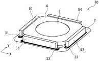
图1是示出具备本公开的一个实施方式涉及的抖动校正模块的相机的抖动校正机构的例子的示意性截面图。1 is a schematic cross-sectional view illustrating an example of a camera shake correction mechanism including a shake correction module according to an embodiment of the present disclosure.
图2是示出本公开的一个实施方式涉及的抖动校正模块的示意性立体图。FIG. 2 is a schematic perspective view illustrating a shake correction module according to an embodiment of the present disclosure.
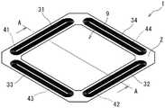
图3是示出本公开的一个实施方式涉及的柔性印刷布线板的示意性立体图。FIG. 3 is a schematic perspective view showing a flexible printed wiring board according to one embodiment of the present disclosure.
图4是图3的柔性印刷布线板的A-A线截面图。4 is an A-A cross-sectional view of the flexible printed wiring board of FIG. 3 .
图5是示出其他实施方式涉及的柔性印刷布线板的截面图。FIG. 5 is a cross-sectional view showing a flexible printed wiring board according to another embodiment.
图6是示出其他实施方式涉及的柔性印刷布线板的截面图。FIG. 6 is a cross-sectional view showing a flexible printed wiring board according to another embodiment.
图7是示出其他实施方式涉及的柔性印刷布线板的截面图。7 is a cross-sectional view showing a flexible printed wiring board according to another embodiment.
图8是示出其他实施方式涉及的柔性印刷布线板的截面图。FIG. 8 is a cross-sectional view showing a flexible printed wiring board according to another embodiment.
图9是示出其他实施方式涉及的柔性印刷布线板的截面图。FIG. 9 is a cross-sectional view showing a flexible printed wiring board according to another embodiment.
具体实施方式Detailed ways
[本公开要解决的技术问题][Technical problem to be solved by this disclosure]
上述现有技术是检测永久磁铁的N极与S极的边界附近的磁通变化来得到线圈板的位置信息的方式,但是作为相机的抖动校正模块,也研究了如下方式:通过作用于线圈的磁力来向消除抖动的方向驱动摄像元件或校正透镜,由此校正抖动。但是,本发明的本发明人们发现,在这种情况下,如果上述线圈的卷绕密度是一定的,则在磁铁发生了位移时的线圈中产生的磁力(推力)根据磁铁与线圈的位置关系而变动。为了提高相机的抖动校正模块的抖动校正的精度,要求减小磁铁发生了位移时的推力的变动。The above-mentioned prior art is a way to obtain the position information of the coil plate by detecting the magnetic flux change near the boundary between the N pole and the S pole of the permanent magnet. However, as a shake correction module of the camera, the following method has also been studied: The magnetic force is used to drive the imaging element or the correction lens in a direction to eliminate shake, thereby correcting the shake. However, the inventors of the present invention have found that in this case, if the winding density of the coil is constant, the magnetic force (thrust) generated in the coil when the magnet is displaced depends on the positional relationship between the magnet and the coil. And change. In order to improve the accuracy of camera shake correction by the camera shake correction module, it is required to reduce the variation in thrust when the magnet is displaced.
本公开是基于这种情况而完成的,其目的在于提供一种能够在抖动校正模块的磁铁发生位移时抑制推力的变动的柔性印刷布线板。The present disclosure has been made based on such circumstances, and an object thereof is to provide a flexible printed wiring board capable of suppressing fluctuations in thrust force when a magnet of a shake correction module is displaced.
[本公开的效果][Effect of this disclosure]
根据本公开的柔性印刷布线板,能够在抖动校正模块的磁铁发生位移时抑制推力的变动。According to the flexible printed wiring board of the present disclosure, it is possible to suppress fluctuations in thrust when the magnet of the shake correction module is displaced.
[本公开的实施方式的说明][Description of Embodiments of the Present Disclosure]
首先,列举本公开的实施方式来进行说明。First, embodiments of the present disclosure will be given and described.
本公开的一方面涉及的柔性印刷布线板具备:基膜,具有绝缘性;以及平面线圈,设置于上述基膜的表面,在俯视观察时,在上述平面线圈的线圈宽度上,相对中心位置位于内侧的布线的数量大于位于外侧的布线的数量。A flexible printed wiring board according to one aspect of the present disclosure includes: a base film having insulating properties; and a planar coil provided on the surface of the base film, and located at a position relative to the center of the coil width of the planar coil when viewed from above. The number of wires on the inside is greater than the number of wires on the outside.
在线圈的卷绕密度一定的情况下,与磁铁位于线圈的中心部的情况相比,磁铁发生了位移时的推力变小。这是因为,线圈产生的推力是通过线圈的卷绕密度与从磁铁产生的磁通密度的相互作用而产生的。因此,本发明的本发明人们发现:通过增大从磁铁产生的磁通密度高且容易产生线圈的推力的线圈的中心部周边区域的布线密度、而减小线圈的外侧的布线密度,从而在线圈的中心部周边区域内,线圈产生的推力提高且磁铁发生位移时变动也变小。在该柔性印刷布线板中,设置于上述基膜的表面的平面线圈在俯视观察时,在上述平面线圈的线圈宽度上,相对中心位置位于内侧的布线的数量大于位于外侧的布线的数量。其结果是,该柔性印刷布线板能够在抖动校正模块的线圈的中心部周边区域内的磁铁发生位移时抑制推力的变动。因此,该柔性印刷布线板特别是在抖动的范围收敛于规定的中心部周边区域内的情况下,可以与磁铁的位移无关地得到稳定的推力,从而抖动校正的精度高。此外,该柔性印刷布线板提高了最大推力,因此也能够应对多片组的透镜等质量大的高性能光学结构。此外,与现有的相同质量的光学结构相比,能够以少的电流量维持推力,因此能够实现省电化。需要指出,本申请中的“推力”是指用于利用磁力而在直线方向上进行驱动的力。When the winding density of the coil is constant, the thrust force when the magnet is displaced becomes smaller than when the magnet is positioned at the center of the coil. This is because the thrust generated by the coil is generated by the interaction between the winding density of the coil and the magnetic flux density generated from the magnet. Therefore, the present inventors of the present invention have found that by increasing the wiring density around the center of the coil where the magnetic flux density generated from the magnet is high and the thrust of the coil is likely to be generated, and reducing the wiring density outside the coil, the online In the area around the center of the coil, the thrust force generated by the coil increases and the fluctuation when the magnet is displaced becomes small. In this flexible printed wiring board, the planar view of the planar coil provided on the surface of the base film has a larger number of wirings located inside the center position than outside the coil width of the planar coil. As a result, the flexible printed wiring board can suppress fluctuations in thrust when the magnets in the area around the center of the coil of the shake correction module are displaced. Therefore, in this flexible printed wiring board, especially when the shake range is within the predetermined center peripheral region, stable thrust can be obtained regardless of the displacement of the magnet, and the accuracy of shake correction is high. In addition, this flexible printed wiring board has increased maximum thrust, so it can also cope with high-mass high-performance optical structures such as multi-element lenses. In addition, compared with the conventional optical structure of the same quality, thrust force can be maintained with a smaller amount of current, so power saving can be realized. It should be noted that the "thrust force" in this application refers to the force for driving in a linear direction by magnetic force.
在该柔性印刷布线板中,优选上述内侧的布线的数量相对于总布线数量的比例为55%以上。通过使上述内侧的布线的数量相对于总布线数量的比例为55%以上,能够在抖动校正模块的磁铁发生位移时进一步降低推力的变动。In this flexible printed wiring board, it is preferable that the ratio of the number of the said inside wiring with respect to the total number of wirings is 55 % or more. By setting the ratio of the number of inner wires to the total number of wires to be 55% or more, it is possible to further reduce fluctuations in thrust force when the magnet of the shake correction module is displaced.
优选上述布线的平均线宽为10μm以上且125μm以下。通过使上述布线的平均线宽为上述范围,容易形成布线,并且容易将布线的厚度及密度设定为所期望的范围。It is preferable that the average line width of the said wiring is 10 micrometers or more and 125 micrometers or less. By making the average line width of the said wiring into the said range, it becomes easy to form a wiring, and it becomes easy to set the thickness and density of a wiring to a desired range.
优选上述外侧的布线的平均线宽相对于上述内侧的布线的平均线宽的比率为1以上且5以下。通过使上述外侧的布线的平均线宽相对于上述内侧的布线的平均线宽的比率为上述范围,容易形成布线,并且容易将布线的厚度及密度设定为所期望的范围。Preferably, the ratio of the average line width of the outer wiring to the average line width of the inner wiring is 1 or more and 5 or less. When the ratio of the average line width of the outer wiring to the average line width of the inner wiring is within the above-mentioned range, it is easy to form the wiring, and it is easy to set the thickness and density of the wiring to a desired range.
优选上述内侧的布线中的相邻的布线间的平均间隔相同。通过使上述内侧的布线中的相邻的布线间的平均间隔相同,容易形成平面线圈。It is preferable that the average interval between adjacent wirings among the inner wirings is the same. The planar coil can be easily formed by making the average interval between adjacent wirings among the inner wirings the same.
优选上述内侧的布线中的相邻的布线间的平均间隔不同。通过使上述内侧的布线中的相邻的布线间的平均间隔不同,上述内侧的布线中的布线密度的调整变得容易。It is preferable that the average interval between adjacent wirings among the inner wirings is different. By varying the average interval between adjacent wirings among the inner wirings, adjustment of the wiring density among the inner wirings becomes easy.
本公开的另一方面涉及的抖动校正模块具备该柔性印刷布线板和永久磁铁。A shake correction module according to another aspect of the present disclosure includes the flexible printed wiring board and a permanent magnet.
该抖动校正模块由于具有该柔性印刷布线板,因此能够在抖动校正模块的磁铁发生位移时抑制推力的变动。因此,该抖动校正模块能够提高相机的抖动校正的精度。Since the shake correction module has the flexible printed wiring board, it is possible to suppress fluctuations in thrust force when the magnet of the shake correction module is displaced. Therefore, the shake correction module can improve the accuracy of camera shake correction.
[本公开的实施方式的详情][Details of Embodiments of the Present Disclosure]
下面,参照附图,详细说明本公开的各实施方式涉及的柔性印刷布线板及抖动校正模块。需要指出,本实施方式的柔性印刷布线板中的“表面和背面”是指将柔性印刷布线板的厚度方向中的校正透镜的配置侧作为“表面”、将与校正透镜的配置侧相反的一侧作为“背面”的方向,而不是指柔性印刷布线板的使用状态下的表面和背面。Hereinafter, the flexible printed wiring board and the shake correction module according to each embodiment of the present disclosure will be described in detail with reference to the drawings. It should be noted that the "front and back" in the flexible printed wiring board of this embodiment refers to the side where the correction lens is arranged in the thickness direction of the flexible printed wiring board as the "surface" and the side opposite to the side where the correction lens is arranged. The side is used as the direction of the "back", not the front and back of the flexible printed wiring board in use.
[相机的抖动校正机构][camera shake correction mechanism]
图1是示出具备本公开的一个实施方式涉及的抖动校正模块的相机的抖动校正机构的例子的示意性截面图。图2是示出本公开的一个实施方式涉及的抖动校正模块的示意性立体图。图3是示出本公开的一个实施方式涉及的柔性印刷布线板的示意性立体图。内置于数码相机、智能手机等的抖动校正机构60在未图示的光学系统与摄像元件80之间相对于光轴垂直地配置有抖动校正模块70。抖动校正模块70具备本公开的一个实施方式涉及的柔性印刷布线板1,校正由抖动引起的被拍摄物的图像模糊。在抖动校正机构60中,以与校正透镜7对置的方式在基板82固定有由CCD(Charge-Coupled Device,电荷耦合器件)等图像传感器构成的摄像元件80。摄像元件80拍摄由上述光学系统成像的被拍摄物图像并转换为电信号。1 is a schematic cross-sectional view illustrating an example of a camera shake correction mechanism including a shake correction module according to an embodiment of the present disclosure. FIG. 2 is a schematic perspective view illustrating a shake correction module according to an embodiment of the present disclosure. FIG. 3 is a schematic perspective view showing a flexible printed wiring board according to one embodiment of the present disclosure. In the
如图3所示,在基膜2的表面侧层叠有平面线圈31、32、33、34,在基膜2的背面侧层叠有未图示的平面线圈41、42、43、44。在图1的基板82主要层叠有未图示的绝缘层,该绝缘层用于防止上述平面线圈31、32、33、34及平面线圈41、42、43、44与其他部件等接触引起的损伤及短路。绝缘层优选除了有意设置的开口、切口以外将基板82的外表面整面覆盖。绝缘层能够使用阻焊膜、覆盖层等形成,其中优选通过感光性干膜的固化而形成。As shown in FIG. 3 ,
<抖动校正模块><Shake correction module>
该抖动校正模块70具备该柔性印刷布线板1和永久磁铁51、52、53、54。The
四片永久磁铁51、52、53、54配置于磁铁保持件6的周围。此外,在磁铁保持件6的中央保持有校正透镜7。上述永久磁铁51、52、53、54在与未图示的光学系统的光轴方向垂直的方向上相互分离,并且永久磁铁51、52与永久磁铁53、54相互对置地配置。此外,永久磁铁51、52、53、54在与上述光轴方向垂直的方向上极化为N极和S极。在图1的永久磁铁51及永久磁铁52中,相对的永久磁铁51的磁极92和永久磁铁52的磁极93相同。例如在上述磁极92和磁极93为N极的情况下,永久磁铁51的磁极91和永久磁铁52的磁极94为S极。一条平面线圈31、32、33、34及平面线圈41、42、43、44在与永久磁铁51、52、53、54的长度方向平行的面内卷绕成多圈漩涡状。此外,平面线圈31、32、33、34及平面线圈41、42、43、44与永久磁铁51、52、53、54以非接触的状态对置地配置。平面线圈31、32、33、34及平面线圈41、42、43、44始终分别位于四片永久磁铁51、52、53、54的磁场内。Four
如果电流流过平面线圈31、32、33、34及平面线圈41、42、43、44,则产生永久磁铁51、52、53、54的磁场与由流过平面线圈31、32、33、34及平面线圈41、42、43、44的电流产生的磁场的相互作用。例如,如果电流流过平面线圈31、32、33、34及平面线圈41、42、43、44,则按照弗莱明左手定则,在平面线圈31、32、33、34及平面线圈41、42、43、44中产生电磁力、即推力。其结果,能够与永久磁铁51、52、53、54一起驱动磁铁保持件6的中央的校正透镜7。抖动校正模块70利用作用于平面线圈31、32、33、34及平面线圈41、42、43、44的磁力,从而向消除抖动的方向驱动校正透镜7,由此校正抖动。由此,该抖动校正模块70由于具备该柔性印刷布线板1,因此能够在抖动校正模块70的永久磁铁51、52、53、54发生位移时抑制推力的变动。因此,该抖动校正模块70能够提高相机的抖动校正的精度。If electric current flows through
<柔性印刷布线板><Flexible printed wiring board>
图3所示的该柔性印刷布线板1具备具有挠性及绝缘性的基膜2、以及设置于上述基膜2的表面的平面线圈31、32、33、34及平面线圈41、42、43、44等。The flexible printed
(基膜)(basement membrane)
基膜2以合成树脂为主成分,具有挠性及电绝缘性。基膜2是用于形成平面线圈31、32、33、34及平面线圈41、42、43、44等的基材层。需要指出,“主成分”是指以质量换算计含有比例最大的成分,例如是指含量为50质量%以上的成分。此外,基膜2具备方形的切口9,具有四方环形状。The
作为上述合成树脂例如可以列举聚酰亚胺、聚对苯二甲酸乙二醇酯、液晶聚合物、氟树脂等。As said synthetic resin, a polyimide, a polyethylene terephthalate, a liquid crystal polymer, a fluororesin, etc. are mentioned, for example.
作为基膜2的平均厚度的下限优选为5μm,更优选为10μm。另一方面,作为基膜2的平均厚度的上限优选为50μm,更优选为40μm。如果基膜2的平均厚度小于上述下限,则基膜2的绝缘强度有可能不充分。相反,如果基膜2的平均厚度超过上述上限,则该柔性印刷布线板1有可能不必要地变厚、挠性有可能变得不充分。需要指出,在本说明书中“平均厚度”是指任意十点的厚度的平均值。The lower limit of the average thickness of the
(平面线圈)(planar coil)
如图3所示,在四方环形状的基膜2上,沿各片在基膜2的表面侧及背面侧层叠有四对平面线圈31、32、33、34及平面线圈41、42、43、44。需要指出,平面线圈也可以仅层叠于基膜2的表面侧。As shown in FIG. 3, four pairs of
平面线圈31、32、33、34及平面线圈41、42、43、44是对具有导电性的材料进行图案化而形成的。作为形成平面线圈31、32、33、34及平面线圈41、42、43、44的材料,例如优选铜、镍、银等金属,其中特别优选比较廉价且电阻小的铜。The planar coils 31 , 32 , 33 , 34 and the
基膜2的表面固定有四个平面线圈31、32、33、34,在基膜2的背面固定有未图示的四个平面线圈41、42、43、44。上述永久磁铁51、52能够相对于平面线圈31、32、41、42在X方向上往返移动,永久磁铁53、54能够相对于平面线圈33、34、43、44在Y方向上往返移动。由此,在抖动校正中,校正透镜7使通过上述光学系统成像的被拍摄物图像在摄像元件80的摄像面上在X方向及Y方向上位移,并使该位移与拍摄时产生的抖动、即摄像面上的振动对应,从而抵消上述位移来校正抖动。Four
图4是图3的柔性印刷布线板1的A-A线剖视图。上述平面线圈31、41在俯视观察时,在上述平面线圈的线圈宽度W上,相对中心位置P位于内侧的布线31b、41b的数量大于位于外侧的布线31a、41a的数量。因此,该柔性印刷布线板1能够在抖动校正模块70的线圈的中心部周边区域内的永久磁铁51、52、53、54发生位移时抑制推力的变动。因此,该柔性印刷布线板特别是在抖动的范围收敛于规定的中心部周边区域内的情况下,可以与磁铁的位移无关地得到稳定的推力,从而抖动校正的精度高。此外,由于该柔性印刷布线板的最大推力提高,所以也能够应对多片组的透镜等质量大的高性能光学结构。此外,与现有的相同质量的光学结构相比,能够以少的电流量维持推力,因此能够实现省电化。FIG. 4 is an A-A cross-sectional view of the flexible printed
在该柔性印刷布线板1中,作为上述内侧的布线的数量相对于总布线数量的比例的下限,优选为55%,更优选为60%。通过使上述内侧的布线的数量相对于总布线数量的比例为上述范围,能够在抖动校正模块的磁铁发生位移时进一步降低推力的变动。In this flexible printed
作为构成平面线圈31、32、33、34及平面线圈41、42、43、44的布线的平均厚度的上限,优选为100μm,更优选为80μm。如果上述平均厚度超过上述上限,则有可能违背该柔性印刷布线板1的薄型化的要求。另一方面,作为布线的平均厚度的下限,优选为10μm,更优选为20μm。如果上述平均厚度小于上述下限,则电阻有可能变大。The upper limit of the average thickness of the wiring constituting the
优选上述内侧的布线中的相邻的布线间的平均间隔相同。通过使上述内侧的布线中的相邻的布线间的平均间隔相同,容易形成平面线圈。此外,如图5的柔性印刷布线板20所示,在内侧的布线231b、241b中的相邻的布线间的平均间隔相同的情况下,外侧的布线231a、241a中的相邻的布线间的平均间隔也可以不相同。此外,在柔性印刷布线板20中同样地,平面线圈231、241中,在线圈宽度W上,相对中心位置P位于内侧的布线231b、241b的数量也大于位于外侧的布线231a、241a的数量。It is preferable that the average interval between adjacent wirings among the inner wirings is the same. The planar coil can be easily formed by making the average interval between adjacent wirings among the inner wirings the same. In addition, as shown in the flexible printed
作为相邻的布线间的平均间隔的下限,优选为5μm,更优选为8μm。另一方面,作为上述平均间隔的上限,优选为120μm,更优选为110μm。如果上述平均间隔小于上述下限,则有可能变得不容易形成布线。相反,如果上述平均间隔超过上述上限,则有可能难以得到所期望的布线密度。需要指出,“平均间隔”是指任意三点的间隔的平均值。The lower limit of the average interval between adjacent wirings is preferably 5 μm, more preferably 8 μm. On the other hand, the upper limit of the average interval is preferably 120 μm, and more preferably 110 μm. If the above-mentioned average interval is smaller than the above-mentioned lower limit, it may become difficult to form wiring. Conversely, if the above-mentioned average interval exceeds the above-mentioned upper limit, it may be difficult to obtain a desired wiring density. It should be noted that the "average interval" refers to the average value of intervals of any three points.
作为构成平面线圈31、32、33、34及平面线圈41、42、43、44的布线的平均线宽的下限,优选为10μm,更优选为20μm。另一方面,作为上述布线的平均线宽的上限,优选为125μm,更优选为115μm。如果上述布线的平均线宽小于上述下限,则有可能变得不容易形成上述布线。此外,如果上述布线的平均线宽小于上述下限,则有可能无法充分地增大上述布线的厚度(基膜2的厚度方向的高度)。相反,如果上述布线的平均线宽超过上述上限,则有可能难以得到所期望的布线密度。需要指出,“平均线宽”是指任意三点的宽度的平均值。The lower limit of the average line width of wiring constituting
作为上述外侧的布线的平均线宽相对于上述内侧的布线的平均线宽的比率的下限,优选为1.0,更优选为1.2。另一方面,作为上述平均线宽的比率的上限,优选为5.0,更优选为4.0。在上述平均线宽的比率小于1的情况下,上述平面线圈31、32、33、34及平面线圈41、42、43、44的电阻值有可能上升。如果上述平均线宽的比率超过5,则有可能难以得到所期望的布线密度。The lower limit of the ratio of the average line width of the outer wiring to the average line width of the inner wiring is preferably 1.0, more preferably 1.2. On the other hand, the upper limit of the ratio of the average line width is preferably 5.0, and more preferably 4.0. When the ratio of the average line width is less than 1, the resistance values of the
[柔性印刷布线板的制造方法][Manufacturing method of flexible printed wiring board]
该印刷布线板的制造方法具备在具有绝缘性的基膜的至少一个面侧层叠平面线圈的工序。在上述层叠平面线圈的工序中,在基膜的至少一面侧层叠线圈图案。作为线圈图案的层叠方法,能够使用公知的方法,能够使用减成法、半加成法等。特别是通过使用半加成法,能够高效地得到布线密度高的线圈图案。This method of manufacturing a printed wiring board includes a step of laminating a planar coil on at least one side of an insulating base film. In the step of laminating the planar coil, the coil pattern is laminated on at least one side of the base film. As a lamination method of a coil pattern, a well-known method can be used, and a subtractive method, a semi-additive method, etc. can be used. In particular, a coil pattern with high wiring density can be efficiently obtained by using the semi-additive method.
[其他实施方式][Other implementations]
应当认为,本次公开的实施方式在所有方面都是例示而不是限制性的。本公开的范围不限定于上述实施方式的构成,而由权利要求示出,包括与权利要求等同的含义及范围内的所有变更。It should be considered that the embodiments disclosed this time are illustrative and not restrictive in any respect. The scope of the present disclosure is not limited to the configuration of the above-described embodiments but is shown by the claims, and all changes within the meaning and scope equivalent to the claims are included.
在上述实施方式中,上述内侧的布线中的相邻的布线间的平均间隔相同,但是也可以如图6的柔性印刷布线板10那样,上述内侧的布线中的相邻的布线间的平均间隔不同。通过使上述内侧的布线中的相邻的布线间的平均间隔不同,容易调整上述内侧的布线中的布线密度。柔性印刷布线板10中,内侧的布线131b、141b中的相邻的布线间的平均间隔不同。此外,在柔性印刷布线板10中同样地,平面线圈131、141中,在线圈宽度W上,相对中心位置P位于内侧的布线131b、141b的数量大于位于外侧的布线131a、141a的数量。In the above-described embodiment, the average interval between adjacent wirings among the inner wirings is the same, but the average interval between adjacent wirings among the inner wirings may be equal to that of the flexible printed
在上述实施方式中,上述内侧的布线的平均线宽与上述外侧的布线的平均线宽相同,但是也可以如图7的柔性印刷布线板150那样,上述内侧的布线的平均线宽与上述外侧的布线的平均线宽不同。通过使上述内侧的布线的平均线宽与上述外侧的布线的平均线宽不同,能够抑制电阻值的增大。柔性印刷布线板150中,内侧的布线331b、341b中的相邻的布线间的平均间隔不同。在柔性印刷布线板150的平面线圈331、341中,在线圈宽度W上,相对中心位置P位于内侧的布线331b、341b的数量大于位于外侧的布线331a、341a的数量。此外,外侧的布线331a、341a的平均线宽相对于内侧的布线331b、341b的平均线宽的比率为1以上且5以下。In the above-described embodiment, the average line width of the inner wiring is the same as the average line width of the outer wiring. However, as in the flexible printed
此外,也可以如图8的柔性印刷布线板170那样,上述内侧的布线的平均线宽与上述外侧的布线的平均线宽不同,并且在相同区域内相邻的布线间的平均间隔不同。柔性印刷布线板170的内侧的布线531b、541b的平均线宽与外侧的布线531a、541a的平均线宽不同,并且在内侧区域内及外侧区域内分别相邻的布线间的平均间隔不同。在柔性印刷布线板170的平面线圈531、541中,在线圈宽度W上,相对中心位置P位于内侧的布线531b、541b的数量大于位于外侧的布线531a、541a的数量。此外,外侧的布线531a、541a的平均线宽相对于内侧的布线531b、541b的平均线宽的比率为1以上且5以下。In addition, as in the flexible printed
此外,也可以如图9的柔性印刷布线板160那样,在相同区域内相邻的布线的平均线宽不同。在柔性印刷布线板160的平面线圈431、441中,在线圈宽度W上,相对中心位置P位于内侧的布线431b、441b的数量大于位于外侧的布线431a、441a的数量。此外,外侧的布线431a、441a的平均线宽相对于内侧的布线431b、441b的平均线宽的比率为1以上且5以下。In addition, as in the flexible printed
附图标记说明Explanation of reference signs
1、10、20、150、160、170 柔性印刷布线板1, 10, 20, 150, 160, 170 Flexible printed wiring board
2 基膜2 basement membrane
6 磁铁保持件6 magnet holder
7 校正透镜7 Correction lens
9 切口9 cuts
31、32、33、34、41、42、43、44、131、141、231、241、331、341、431、441、531、541 平面线圈31, 32, 33, 34, 41, 42, 43, 44, 131, 141, 231, 241, 331, 341, 431, 441, 531, 541 planar coil
31a、31b、41a、41b、131a、131b、141a、141b、231a、231b、241a、241b、331a、331b、341a、341b、431a、431b、441a、441b、531a、531b、541a、541b 布线31a, 31b, 41a, 41b, 131a, 131b, 141a, 141b, 231a, 231b, 241a, 241b, 331a, 331b, 341a, 341b, 431a, 431b, 441a, 441b, 531a, 531b, 541a, 541b Wiring
51、52、53、54 永久磁铁51, 52, 53, 54 permanent magnets
60 抖动校正机构60 shake correction mechanism
70 抖动校正模块70 Shake Correction Module
80 摄像元件80 camera elements
82 基板82 substrate
91、92、93、94 磁极91, 92, 93, 94 poles
P 中心位置P center position
W 线圈宽度。W Coil width.
Claims (11)
Priority Applications (1)
| Application Number | Priority Date | Filing Date | Title |
|---|---|---|---|
| CN202310256897.3ACN116056318A (en) | 2020-03-27 | 2021-03-24 | Flexible Printed Wiring Board |
Applications Claiming Priority (3)
| Application Number | Priority Date | Filing Date | Title |
|---|---|---|---|
| JP2020-059088 | 2020-03-27 | ||
| JP2020059088 | 2020-03-27 | ||
| PCT/JP2021/012407WO2021193771A1 (en) | 2020-03-27 | 2021-03-24 | Flexible printed wiring board and hand-shaking correction module |
Related Child Applications (1)
| Application Number | Title | Priority Date | Filing Date |
|---|---|---|---|
| CN202310256897.3ADivisionCN116056318A (en) | 2020-03-27 | 2021-03-24 | Flexible Printed Wiring Board |
Publications (2)
| Publication Number | Publication Date |
|---|---|
| CN114175862A CN114175862A (en) | 2022-03-11 |
| CN114175862Btrue CN114175862B (en) | 2023-03-24 |
Family
ID=77890688
Family Applications (2)
| Application Number | Title | Priority Date | Filing Date |
|---|---|---|---|
| CN202180004698.2AActiveCN114175862B (en) | 2020-03-27 | 2021-03-24 | Flexible printed wiring board and jitter correction module |
| CN202310256897.3APendingCN116056318A (en) | 2020-03-27 | 2021-03-24 | Flexible Printed Wiring Board |
Family Applications After (1)
| Application Number | Title | Priority Date | Filing Date |
|---|---|---|---|
| CN202310256897.3APendingCN116056318A (en) | 2020-03-27 | 2021-03-24 | Flexible Printed Wiring Board |
Country Status (4)
| Country | Link |
|---|---|
| US (1) | US11657944B2 (en) |
| JP (2) | JP6985568B1 (en) |
| CN (2) | CN114175862B (en) |
| WO (1) | WO2021193771A1 (en) |
Families Citing this family (2)
| Publication number | Priority date | Publication date | Assignee | Title |
|---|---|---|---|---|
| KR102825969B1 (en)* | 2020-03-12 | 2025-06-27 | 엘지이노텍 주식회사 | Coil substrate for correcting hand-shake and camera module having the same |
| WO2024053425A1 (en)* | 2022-09-07 | 2024-03-14 | 住友電工プリントサーキット株式会社 | Printed wiring board |
Citations (1)
| Publication number | Priority date | Publication date | Assignee | Title |
|---|---|---|---|---|
| JP2013258393A (en)* | 2012-03-26 | 2013-12-26 | Sumitomo Electric Printed Circuit Inc | Flexible printed wiring board and manufacturing method of the same |
Family Cites Families (21)
| Publication number | Priority date | Publication date | Assignee | Title |
|---|---|---|---|---|
| JPS4846810A (en)* | 1971-10-18 | 1973-07-04 | ||
| DE2830732A1 (en)* | 1978-07-13 | 1980-01-31 | Bosch Gmbh Robert | Printed circuit coil deposited as flat spiral - has fixed gap between turns along radius varying in sections |
| JPH01151311A (en) | 1987-12-08 | 1989-06-14 | Murata Mfg Co Ltd | Lc filter |
| JP2002134319A (en)* | 2000-10-23 | 2002-05-10 | Alps Electric Co Ltd | Spiral inductor |
| JP3614816B2 (en)* | 2001-12-26 | 2005-01-26 | 松下電器産業株式会社 | Magnetic element and power source using the same |
| US7196603B2 (en)* | 2003-04-18 | 2007-03-27 | Board Of Regents, The University Of Texas System | Magnetic coil design using optimization of sinusoidal coefficients |
| JP4448298B2 (en)* | 2003-07-14 | 2010-04-07 | アルプス電気株式会社 | Spiral inductor |
| US20060018643A1 (en)* | 2004-07-21 | 2006-01-26 | Stavely Donald J | Magnet configuration for image stabilization |
| JP4584787B2 (en) | 2004-07-26 | 2010-11-24 | Hoya株式会社 | Stage device and camera shake correction device using the stage device |
| US7327952B2 (en) | 2004-07-26 | 2008-02-05 | Pentax Corporation | Stage apparatus and camera shake correction apparatus using the stage apparatus |
| JP2010082501A (en) | 2008-09-29 | 2010-04-15 | Sanyo Electric Co Ltd | Linear motor and portable apparatus equipped with linear motor |
| JP2012244763A (en)* | 2011-05-19 | 2012-12-10 | Sony Corp | Power supply device, power supply system and electronic device |
| CN205303100U (en)* | 2013-07-11 | 2016-06-08 | 株式会社村田制作所 | Electronic component |
| US9177709B2 (en)* | 2013-09-05 | 2015-11-03 | Globalfoundries Inc. | Structure and method for high performance multi-port inductor |
| WO2015079773A1 (en) | 2013-11-28 | 2015-06-04 | 株式会社村田製作所 | Electromagnet, camera-lens driving method, and electromagnet manufacturing method |
| JP6365933B2 (en)* | 2014-07-17 | 2018-08-01 | 住友電工プリントサーキット株式会社 | Flexible printed wiring board, antenna and wireless power feeder |
| CN207692179U (en)* | 2015-08-07 | 2018-08-03 | 株式会社村田制作所 | multilayer substrate |
| KR102560030B1 (en)* | 2016-05-27 | 2023-07-26 | 삼성전자주식회사 | Wireless power receiver and method thereof |
| WO2019194059A1 (en)* | 2018-04-04 | 2019-10-10 | 住友電工プリントサーキット株式会社 | Flexible printed wiring board |
| JP7149114B2 (en)* | 2018-06-21 | 2022-10-06 | ローム株式会社 | Actuator and camera module |
| KR102163060B1 (en)* | 2019-01-16 | 2020-10-08 | 삼성전기주식회사 | Inductor and manufacturing method thereof |
- 2021
- 2021-03-24CNCN202180004698.2Apatent/CN114175862B/enactiveActive
- 2021-03-24WOPCT/JP2021/012407patent/WO2021193771A1/ennot_activeCeased
- 2021-03-24JPJP2021556333Apatent/JP6985568B1/enactiveActive
- 2021-03-24USUS17/627,887patent/US11657944B2/enactiveActive
- 2021-03-24CNCN202310256897.3Apatent/CN116056318A/enactivePending
- 2021-11-24JPJP2021190538Apatent/JP2022033818A/enactivePending
Patent Citations (1)
| Publication number | Priority date | Publication date | Assignee | Title |
|---|---|---|---|---|
| JP2013258393A (en)* | 2012-03-26 | 2013-12-26 | Sumitomo Electric Printed Circuit Inc | Flexible printed wiring board and manufacturing method of the same |
Also Published As
| Publication number | Publication date |
|---|---|
| JP6985568B1 (en) | 2021-12-22 |
| CN114175862A (en) | 2022-03-11 |
| JPWO2021193771A1 (en) | 2021-09-30 |
| CN116056318A (en) | 2023-05-02 |
| WO2021193771A1 (en) | 2021-09-30 |
| US20220208428A1 (en) | 2022-06-30 |
| JP2022033818A (en) | 2022-03-02 |
| US11657944B2 (en) | 2023-05-23 |
Similar Documents
| Publication | Publication Date | Title |
|---|---|---|
| US11309114B2 (en) | Stacked body and method of producing stacked body | |
| CN114175862B (en) | Flexible printed wiring board and jitter correction module | |
| US10983302B2 (en) | Lens driving mechanism | |
| US11662650B2 (en) | Optical element driving mechanism | |
| CN209858825U (en) | Optical element driving mechanism | |
| CN113966606B (en) | Camera device | |
| US12432451B2 (en) | Flexible printed circuit board and image stabilization module | |
| US20220357554A1 (en) | Driving mechanism | |
| CN107561825A (en) | Lens driving mechanism | |
| KR101875066B1 (en) | Image stabilizing coil unit and manufacturing method of this | |
| CN209373236U (en) | Multi-lens camera system and its driving mechanism | |
| US11381147B2 (en) | Driving mechanism | |
| US12028979B2 (en) | Substrate assembly for correcting position of camera module, method for manufacturing same, and camera module including same | |
| CN205539649U (en) | Multilayer coils, lens drivers, camera devices, and electronics | |
| CN114631305A (en) | Coil component for correcting hand trembling and camera module having the same | |
| CN214586186U (en) | Optical element drive mechanism | |
| US12250444B2 (en) | Camera device comprising a structure for disposition of a gyro sensor | |
| US20240161974A1 (en) | Lens barrel, camera, imaging apparatus, and coil component | |
| KR102869730B1 (en) | Camera device | |
| JP6605531B2 (en) | Mobile electromagnetic drive | |
| CN120075580A (en) | Image pickup module and manufacturing method thereof | |
| KR20200128956A (en) | Camera apparatus with improved driving and detection performance | |
| JP2013234958A (en) | Current detecting device |
Legal Events
| Date | Code | Title | Description |
|---|---|---|---|
| PB01 | Publication | ||
| PB01 | Publication | ||
| SE01 | Entry into force of request for substantive examination | ||
| SE01 | Entry into force of request for substantive examination | ||
| GR01 | Patent grant | ||
| GR01 | Patent grant |