CN114171871B - Non-contact adjustable negative group delay circuit based on dielectric resonator and its construction method - Google Patents
Non-contact adjustable negative group delay circuit based on dielectric resonator and its construction methodDownload PDFInfo
- Publication number
- CN114171871B CN114171871BCN202111355973.3ACN202111355973ACN114171871BCN 114171871 BCN114171871 BCN 114171871BCN 202111355973 ACN202111355973 ACN 202111355973ACN 114171871 BCN114171871 BCN 114171871B
- Authority
- CN
- China
- Prior art keywords
- dielectric resonator
- microstrip line
- group delay
- circuit
- dielectric
- Prior art date
- Legal status (The legal status is an assumption and is not a legal conclusion. Google has not performed a legal analysis and makes no representation as to the accuracy of the status listed.)
- Active
Links
Images


Classifications
- H—ELECTRICITY
- H01—ELECTRIC ELEMENTS
- H01P—WAVEGUIDES; RESONATORS, LINES, OR OTHER DEVICES OF THE WAVEGUIDE TYPE
- H01P5/00—Coupling devices of the waveguide type
- H01P5/12—Coupling devices having more than two ports
- H—ELECTRICITY
- H01—ELECTRIC ELEMENTS
- H01P—WAVEGUIDES; RESONATORS, LINES, OR OTHER DEVICES OF THE WAVEGUIDE TYPE
- H01P11/00—Apparatus or processes specially adapted for manufacturing waveguides or resonators, lines, or other devices of the waveguide type
- H—ELECTRICITY
- H01—ELECTRIC ELEMENTS
- H01P—WAVEGUIDES; RESONATORS, LINES, OR OTHER DEVICES OF THE WAVEGUIDE TYPE
- H01P3/00—Waveguides; Transmission lines of the waveguide type
- H01P3/02—Waveguides; Transmission lines of the waveguide type with two longitudinal conductors
- H01P3/08—Microstrips; Strip lines
Landscapes
- Engineering & Computer Science (AREA)
- Manufacturing & Machinery (AREA)
- Control Of Motors That Do Not Use Commutators (AREA)
Abstract
Translated fromChinese
Description
Translated fromChinese技术领域technical field
本发明涉及微波工程技术领域,具体而言涉及基于介质谐振器的非接触式可调负群时延电路及构建方法。The invention relates to the technical field of microwave engineering, in particular to a non-contact adjustable negative group delay circuit based on a dielectric resonator and a construction method.
背景技术Background technique
在现代通信系统中,复杂的电路互连结构引起的群时延效应是信号失真的重要原因之一。为了避免由群时延引起的信号失真,常常采用负群时延电路作为均衡器来补偿群时延的变化。负群时延指的是群时延为负值,即输出信号比输入信号提前出现这一异常的电磁传播现象。群时延这一参量指的是相位关于角频率的负导数,负群时延特性的相位会随着频率出现正变化率,这一参数反映了电路中信号相位的色散情况。爱因斯坦相对论中指出,在真空环境中没有任何物质能够超越光速,负群时延和超光速传播看上去好像违背了常规认知,但在二十世纪七十年代Garrett和Mccummbe从理论上证明了:当介质中存在异常色散时波的群速度为负是存在的并且符合因果规律的,该理论的证实是在相对苛刻的条件下进行的。In modern communication systems, the group delay effect caused by the complex circuit interconnection structure is one of the important reasons for signal distortion. In order to avoid signal distortion caused by group delay, a negative group delay circuit is often used as an equalizer to compensate for changes in group delay. Negative group delay means that the group delay is negative, that is, the abnormal electromagnetic propagation phenomenon occurs in the output signal earlier than the input signal. The parameter of group delay refers to the negative derivative of the phase with respect to the angular frequency. The phase of the negative group delay characteristic will have a positive rate of change with frequency. This parameter reflects the dispersion of the signal phase in the circuit. Einstein's theory of relativity pointed out that nothing can exceed the speed of light in a vacuum environment. Negative group delay and superluminal propagation seem to be contrary to conventional knowledge, but in the 1970s Garrett and McCummbe theoretically proved that Now: when there is anomalous dispersion in the medium, the group velocity of the wave is negative and it is in line with the causal law, and the verification of the theory is carried out under relatively harsh conditions.
近年来,负群时延现象已在电子电路中实现,并在各种通信系统中得到广泛应用。国外已采用各种结构来实现负群时延电路或滤波器,比如缺陷微带结构、缺陷接地结构、3-dB混合耦合器和传输线等,然而,这些研究中的结构都只能实现固定的中心频率和负群时延,因此,研究设计中心频率和群时延值可配置负群时延电路对于提高微波系统性能具有重要实际意义。目前大多可调谐负群时延电路采用加载可变电阻、变容二极管、pin二极管等接触式方法来实现可调功能,缺少基于空间耦合的角度实现非接触式可调负群时延电路的研究与设计。In recent years, the negative group delay phenomenon has been realized in electronic circuits and widely used in various communication systems. Various structures have been adopted abroad to realize negative group delay circuits or filters, such as defected microstrip structures, defected ground structures, 3-dB hybrid couplers and transmission lines, etc. However, the structures in these studies can only achieve fixed Center frequency and negative group delay, therefore, research and design of center frequency and group delay value configurable negative group delay circuit is of great practical significance for improving the performance of microwave systems. At present, most tunable negative group delay circuits use contact methods such as loading variable resistors, varactors, pin diodes, etc. to achieve adjustable functions. There is a lack of research on non-contact adjustable negative group delay circuits based on the angle of spatial coupling. with design.
发明内容SUMMARY OF THE INVENTION
本发明的目的在于提供一种基于介质谐振器的非接触式可调负群时延电路及构建方法,以解决现有技术中的问题。The purpose of the present invention is to provide a non-contact adjustable negative group delay circuit based on a dielectric resonator and a construction method to solve the problems in the prior art.
为实现上述目的,本发明提供如下技术方案:To achieve the above object, the present invention provides the following technical solutions:
一种基于介质谐振器的非接触式可调负群时延电路,包括介质谐振器、介质基板、介质盖板、以及至少一个支撑柱,介质基板与介质盖板以彼此平行姿态通过各个支撑柱相连,各个支撑柱的上、下两端分别垂直于介质基板、介质盖板;A non-contact adjustable negative group delay circuit based on a dielectric resonator, comprising a dielectric resonator, a dielectric substrate, a dielectric cover, and at least one support column, the dielectric substrate and the dielectric cover pass through each support column in an attitude parallel to each other connected, the upper and lower ends of each support column are perpendicular to the dielectric substrate and the dielectric cover respectively;
所述介质基板面向介质盖板的一面为上表面,介质基板的底部接地,介质基板的上表面布设有环形微带线、第一微带线、以及第二微带线,环形微带线的任意一端与第一微带线的一端相连,第一微带线的另一端与第二微带线的任意位置相连,第二微带线的两端分别连接输入端口、输出端口,输入端口、输出端口分别构成非接触式可调负群时延电路的输入端、输出端;The side of the dielectric substrate facing the dielectric cover plate is the upper surface, the bottom of the dielectric substrate is grounded, and the upper surface of the dielectric substrate is provided with an annular microstrip line, a first microstrip line, and a second microstrip line. Either end is connected to one end of the first microstrip line, the other end of the first microstrip line is connected to any position of the second microstrip line, and the two ends of the second microstrip line are respectively connected to the input port, the output port, the input port, The output ports respectively constitute the input end and the output end of the non-contact adjustable negative group delay circuit;
介质谐振器设置于介质基板上表面对应环形微带线所围的区域内,介质谐振器的底部开设有通孔,通孔内部设有与第一调谐螺丝相匹配的螺纹,第一调谐螺丝的顶部与介质谐振器的底部相连,第一调谐螺丝与介质基板相垂直;The dielectric resonator is arranged on the upper surface of the dielectric substrate corresponding to the area surrounded by the annular microstrip line. The bottom of the dielectric resonator is provided with a through hole, and the interior of the through hole is provided with a thread matching the first tuning screw. The top is connected to the bottom of the dielectric resonator, and the first tuning screw is perpendicular to the dielectric substrate;
所述介质盖板面向介质基板的一面布设有金属调谐圆盘,金属调谐圆盘的顶部开设有通孔,通孔内部设有与第二调谐螺丝相匹配的螺纹,第二调谐螺丝的顶部与金属调谐圆盘的顶部相连,第二调谐螺丝与介质盖板相垂直;A metal tuning disk is arranged on the side of the medium cover facing the medium substrate, a through hole is opened on the top of the metal tuning disk, and a thread matching the second tuning screw is arranged inside the through hole, and the top of the second tuning screw is matched with the second tuning screw. The top of the metal tuning disc is connected, and the second tuning screw is perpendicular to the medium cover;
所述金属调谐圆盘与介质谐振器在投影方向有重叠,介质谐振器、金属调谐圆盘分别通过第一调谐螺丝、第二调谐螺丝的转动,实现介质谐振器与金属调谐圆盘纵面上的距离调节。The metal tuning disk and the dielectric resonator overlap in the projection direction, and the dielectric resonator and the metal tuning disk are respectively rotated by the first tuning screw and the second tuning screw to realize the longitudinal plane of the dielectric resonator and the metal tuning disk. distance adjustment.
进一步地,金属调谐圆盘位于介质谐振器的正上方。Further, the metal tuning disk is located directly above the dielectric resonator.
进一步地,环形微带线的内径大于介质谐振器的外径。Further, the inner diameter of the annular microstrip line is larger than the outer diameter of the dielectric resonator.
进一步地,介质谐振器等效为等效电感L、等效电阻R、等效电容C并联组成的RLC电路,介质谐振器与环形微带线耦合,根据以下公式:Further, the dielectric resonator is equivalent to an RLC circuit composed of an equivalent inductance L, an equivalent resistance R, and an equivalent capacitance C in parallel, and the dielectric resonator is coupled with the annular microstrip line according to the following formula:

获得介质谐振器与环形微带线耦合的耦合系数g,其中,Q为介质谐振器自身的品质因数,Qe为与环形微带线耦合后的介质谐振器的品质因数,RL为等效电感的电阻,ω0为介质谐振器的谐振频率,
根据以下公式:According to the following formula:

获得介质谐振器与环形微带线耦合后,介质谐振器的等效串联阻抗ZDR,j为虚部单位,ω为介质谐振器与环形微带线耦合后耦合电路的谐振频率。After the dielectric resonator is coupled with the annular microstrip line, the equivalent series impedance ZDR of the dielectric resonator is obtained, j is the unit of the imaginary part, and ω is the resonant frequency of the coupling circuit after the dielectric resonator is coupled with the annular microstrip line.
进一步地,耦合电路的散射参数[S]表示为:Further, the scattering parameter [S] of the coupling circuit is expressed as:

其中,以环形微带线(3)两端之间的任意一点将环形微带线(3)分为两部分,l1、l2分别为两部分的长度,其中l1为环形微带线(3)与第一微带线(4)相接一端与该任意一点之间的长度,l2为该任意一点与环形微带线(3)另一端之间的长度,β1、β2分别为l1、l2对应的相移常数;Wherein, the annular microstrip line (3) is divided into two parts by any point between the two ends of the annular microstrip line (3), l1 and l2 are the lengths of the two parts respectively, wherein l1 is the annular microstrip line (3) The length between the end connected to the first microstrip line (4) and the arbitrary point, l2 is the length between the arbitrary point and the other end of the annular microstrip line (3), β1 , β2 are the phase shift constants corresponding to l1 and l2 respectively;
基于耦合电路的散射参数[S],获得耦合电路的输入回波损耗

根据介质谐振器的等效串联阻抗ZDR和耦合电路的输出回波损耗S21,根据以下公式:According to the equivalent series impedance ZDR of the dielectric resonator and the output return loss S21 of the coupling circuit, according to the following formula:

获得等效RLC电路的插入损耗S21,其中,i为虚部单位,θ为环形微带线对应的拟合长度;Obtain the insertion loss S21 of the equivalent RLC circuit, where i is the unit of the imaginary part, and θ is the fitting length corresponding to the annular microstrip line;
进一步获得等效RLC电路插入损耗的相位,根据公式:Further obtain the phase of the equivalent RLC circuit insertion loss, according to the formula:


其中,
进一步地,基于等效RLC电路的群时延函数τ(ω),当ω=ω0时,

当ω趋向于0时,等效RLC电路的群时延函数根据以下公式:When ω tends to 0, the group delay function of the equivalent RLC circuit is according to the following formula:

根据上述公式,可调负群时延电路通过调节介质谐振器与环形微带线的耦合系数g和介质谐振器的品质因数Q来调节耦合电路的群时延值的大小,通过改变介质谐振器与环形微带线的距离,改变耦合系数g的大小,即通过调节第一调谐螺丝改变电路的耦合系数g;According to the above formula, the adjustable negative group delay circuit adjusts the value of the group delay value of the coupling circuit by adjusting the coupling coefficient g between the dielectric resonator and the annular microstrip line and the quality factor Q of the dielectric resonator. The distance from the annular microstrip line changes the size of the coupling coefficient g, that is, the coupling coefficient g of the circuit is changed by adjusting the first tuning screw;
通过调节第二调谐螺丝改变介质谐振器与金属调谐圆盘之间的距离,改变电路的耦合系数g的大小,进一步改变介质谐振器的品质因数Qe,即通过调节第二调谐螺丝改变电路的耦合系数g。By adjusting the second tuning screw, the distance between the dielectric resonator and the metal tuning disk is changed, the coupling coefficient g of the circuit is changed, and the quality factor Qe of the dielectric resonator is further changed. Coupling coefficient g.
本发明的另一方面提出一种基于介质谐振器的非接触式可调负群时延电路构建方法,包括以下步骤:Another aspect of the present invention provides a method for constructing a non-contact adjustable negative group delay circuit based on a dielectric resonator, comprising the following steps:
步骤S1、获得介质谐振器与环形微带线耦合的耦合系数g,进一步得到介质谐振器与环形微带线耦合后,介质谐振器的等效串联阻抗ZDR;Step S1, obtain the coupling coefficient g of the coupling between the dielectric resonator and the annular microstrip line, and further obtain the equivalent series impedance ZDR of the dielectric resonator after the dielectric resonator is coupled with the annular microstrip line;
步骤S2、基于耦合电路的散射参数[S],获得耦合电路的输入回波损耗S11和插入损耗S21;Step S2, based on the scattering parameter [S] of the coupling circuit, obtain the input return loss S11 and the insertion loss S21 of the coupling circuit;
步骤S3、根据等效RLC电路的插入损耗S21获得插入损耗的相位,基于相位和群时延的定义,获得等效RLC电路的群时延函数τ(ω);Step S3, obtaining the phase of the insertion loss according to the insertion lossS21 of the equivalent RLC circuit, and obtaining the group delay function τ(ω) of the equivalent RLC circuit based on the definitions of the phase and the group delay;
步骤S4、利用群时延函数τ(ω)确定非接触式可调负群时延电路中的各参数值,根据参数值获得对应的非接触式可调负群时延电路。Step S4: Determine each parameter value in the non-contact adjustable negative group delay circuit by using the group delay function τ(ω), and obtain the corresponding non-contact adjustable negative group delay circuit according to the parameter values.
本发明所述基于介质谐振器的非接触式可调负群时延电路及构建方法,采用以上技术方案与现有技术相比,具有以下技术效果:The non-contact adjustable negative group delay circuit and construction method based on the dielectric resonator of the present invention, using the above technical solution compared with the prior art, has the following technical effects:
1、本专利采用环形耦合微带线来耦合介质谐振器,相比于常见的直微带线耦合,耦合强度更高,耦合效果更好,耦合效果决定了电路群时延值的大小,因此能够获得更大的群时延值,本专利提出的负群时延电路负群时延值最大能够达到-4.6ns,性能更优;1. This patent uses ring-coupling microstrip lines to couple the dielectric resonators. Compared with the common straight microstrip line coupling, the coupling strength is higher and the coupling effect is better. The coupling effect determines the delay value of the circuit group. Therefore, A larger group delay value can be obtained. The negative group delay value of the negative group delay circuit proposed in this patent can reach a maximum of -4.6ns, with better performance;
2、本专利除了采用常见的控制介质谐振器与基板高度的方法控制耦合外,还创新性地采用了空间耦合的方法,通过在介质谐振器的上方放置一个可调谐金属圆环,调节介质谐振器的加载Q值,可以从结果中看出,空间耦合调节的方式对群时延值大小的影响略小,控制介质谐振器高度的方法适用于粗调,空间耦合调节方式适合精调,这样使得本专利提出的负群时延电路能更好地运用于各种通信系统中。2. In addition to the common method of controlling the height of the dielectric resonator and the substrate to control the coupling, this patent also innovatively adopts the method of spatial coupling. By placing a tunable metal ring above the dielectric resonator, the dielectric resonance is adjusted. It can be seen from the results that the influence of the spatial coupling adjustment method on the value of the group delay is slightly smaller, the method of controlling the height of the dielectric resonator is suitable for rough adjustment, and the spatial coupling adjustment method is suitable for fine adjustment, so that The negative group delay circuit proposed in this patent can be better used in various communication systems.
3、本专利所提出的方法,由于采用环形微带线的形式,一个介质谐振器单独耦合到一个环形微带线上,受到的影响更小,有载Q值更高。本专利也可以采用多个介质谐振器耦合到多个环形微带线,环形微带线再加载到微带线上的形式,来实现多频负群时延电路,或者采用多个本专利提出的电路,通过调节耦合得到不同的频率,级联后也可以实现多频负群时延电路。3. In the method proposed in this patent, due to the use of a ring microstrip line, a dielectric resonator is independently coupled to a ring microstrip line, which is less affected and has a higher on-load Q value. In this patent, multiple dielectric resonators can also be coupled to multiple annular microstrip lines, and the annular microstrip lines are then loaded onto the microstrip lines to realize multi-frequency negative group delay circuits, or multiple Different frequencies can be obtained by adjusting the coupling, and the multi-frequency negative group delay circuit can also be realized after cascading.
综上所述,本专利提出的电路拥有耦合效果更好,负群时延值更大,可调范围更广的优点,也可以通过级联实现多频负群时延电路。To sum up, the circuit proposed in this patent has the advantages of better coupling effect, larger negative group delay value and wider adjustable range, and a multi-frequency negative group delay circuit can also be realized by cascading.
附图说明Description of drawings
图1为本发明示例性实施例的非接触式可调负群时延电路的三维结构图;1 is a three-dimensional structural diagram of a non-contact adjustable negative group delay circuit according to an exemplary embodiment of the present invention;
图2(a)为本发明示例性实施例的介质谐振器与微带线耦合的电路结构示意图;FIG. 2(a) is a schematic diagram of a circuit structure for coupling between a dielectric resonator and a microstrip line according to an exemplary embodiment of the present invention;
图2(b)为本发明示例性实施例的介质谐振器与微带线耦合的等效电路图;FIG. 2(b) is an equivalent circuit diagram of a dielectric resonator coupled with a microstrip line according to an exemplary embodiment of the present invention;
图3为本发明示例性实施例的非接触式可调负群时延电路的侧视图;3 is a side view of a non-contact adjustable negative group delay circuit according to an exemplary embodiment of the present invention;
图4为本发明示例性实施例的非接触式可调负群时延电路的俯视图;4 is a top view of a non-contact adjustable negative group delay circuit according to an exemplary embodiment of the present invention;
图5(a)为本发明通过调节第一调谐螺丝调节负群时延电路性能的群时延结果示意图;5(a) is a schematic diagram of the group delay result of adjusting the performance of the negative group delay circuit by adjusting the first tuning screw according to the present invention;
图5(b)为本发明通过调节第一调谐螺丝调节负群时延电路性能的回波损耗结果示意图;5(b) is a schematic diagram of the return loss result of adjusting the performance of the negative group delay circuit by adjusting the first tuning screw according to the present invention;
图5(c)为本发明通过调节第一调谐螺丝调节负群时延电路性能的插入损耗结果示意图;5(c) is a schematic diagram of the insertion loss result of the present invention adjusting the performance of the negative group delay circuit by adjusting the first tuning screw;
图6(a)为本发明通过调节第二调谐螺丝调节负群时延电路性能的群时延结果示意图;6(a) is a schematic diagram of the group delay result of adjusting the performance of the negative group delay circuit by adjusting the second tuning screw according to the present invention;
图6(b)为本发明通过调节第二调谐螺丝调节负群时延电路性能的回波损耗结果示意图;Figure 6(b) is a schematic diagram of the return loss result of the present invention adjusting the performance of the negative group delay circuit by adjusting the second tuning screw;
图6(c)为本发明通过调节第二调谐螺丝调节负群时延电路性能的插入损耗结果示意图。FIG. 6( c ) is a schematic diagram of the insertion loss result of adjusting the performance of the negative group delay circuit by adjusting the second tuning screw according to the present invention.
具体实施方式Detailed ways
为了更了解本发明的技术内容,特举具体实施例并配合所附图式说明如下。In order to better understand the technical content of the present invention, specific embodiments are given and described below in conjunction with the accompanying drawings.
在本发明中参照附图来描述本发明的各方面,附图中示出了许多说明性实施例。本发明的实施例不局限于附图所示。应当理解,本发明通过上面介绍的多种构思和实施例,以及下面详细描述的构思和实施方式中的任意一种来实现,这是因为本发明所公开的构思和实施例并不限于任何实施方式。另外,本发明公开的一些方面可以单独使用,或者与本发明公开的其他方面的任何适当组合来使用。Aspects of the invention are described herein with reference to the accompanying drawings, in which a number of illustrative embodiments are shown. Embodiments of the present invention are not limited to those shown in the accompanying drawings. It should be understood that the present invention can be implemented by any of the various concepts and embodiments described above, as well as the concepts and embodiments described in detail below, since the concepts and embodiments disclosed herein are not limited to any implementation Way. Additionally, some aspects of the present disclosure may be used alone or in any suitable combination with other aspects of the present disclosure.
结合图1本发明示例性实施例的非接触式可调负群时延电路的三维结构图,本发明提出基于介质谐振器的非接触式可调负群时延电路,包括介质谐振器1、介质基板6、介质盖板8、以及至少一个支撑柱7,介质基板6与介质盖板8以彼此平行姿态通过各个支撑柱7相连,各个支撑柱7的上、下两端分别垂直于介质基板6、介质盖板8;With reference to the three-dimensional structural diagram of the non-contact adjustable negative group delay circuit according to an exemplary embodiment of the present invention, the present invention proposes a non-contact adjustable negative group delay circuit based on a dielectric resonator, including a
所述介质基板6面向介质盖板8的一面为上表面,介质基板6的底部接地,介质基板6的上表面布设有环形微带线3、第一微带线4、以及第二微带线5,环形微带线3的任意一端与第一微带线4的一端相连,第一微带线4的另一端与第二微带线5的任意位置相连,第二微带线5的两端分别连接输入端口51、输出端口52,输入端口51、输出端口52分别构成非接触式可调负群时延电路的输入端、输出端;The side of the
介质谐振器1设置于介质基板6上表面对应环形微带线3所围的区域内,介质谐振器1的底部开设有通孔,通孔内部设有与第一调谐螺丝2相匹配的螺纹,第一调谐螺丝2的顶部与介质谐振器1的底部相连,第一调谐螺丝2与介质基板6相垂直;The
所述介质盖板8面向介质基板6的一面布设有金属调谐圆盘9,金属调谐圆盘9的顶部开设有通孔,通孔内部设有与第二调谐螺丝10相匹配的螺纹,第二调谐螺丝10的顶部与金属调谐圆盘9的顶部相连,第二调谐螺丝10与介质盖板8相垂直;The side of the
所述金属调谐圆盘9与介质谐振器1在投影方向有重叠,介质谐振器1、金属调谐圆盘9分别通过第一调谐螺丝2、第二调谐螺丝10的转动,实现介质谐振器1与金属调谐圆盘9在纵面上的距离调节。The
作为优选方案,金属调谐圆盘9位于介质谐振器1的正上方。As a preferred solution, the
作为优选方案,环形微带线3的内径大于介质谐振器1的外径。As a preferred solution, the inner diameter of the
实施例Example
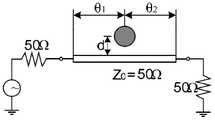
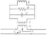
如图2(a)所示,当介质谐振器放在微带线附近时,会与微带线的边缘磁场耦合,设介质谐振器两边的微带线电长度分别为θ1和θ2,介质谐振器的中心点与微带线的距离为d,即耦合距离d。微带线一端接输入电压源和50Ω的负载,输入电压源的另一端接地,微带线的另一端接50Ω的输出负载,输出负载的另一端接地。图2(a)中的电路可以等效为如图2(b)所示的RLC电路,介质谐振器耦合时表现为在微带线上的一个串联负载,介质谐振器可以等效成一个由等效电感L,等效电阻R,等效电容C组成的并联电路,与微带线耦合的模型为变压器的圈数比N。As shown in Fig. 2(a), when the dielectric resonator is placed near the microstrip line, it will be coupled with the fringe magnetic field of the microstrip line. Let the electrical lengths of the microstrip line on both sides of the dielectric resonator be θ1 and θ2 respectively, The distance between the center point of the dielectric resonator and the microstrip line is d, that is, the coupling distance d. One end of the microstrip line is connected to the input voltage source and the 50Ω load, the other end of the input voltage source is grounded, the other end of the microstrip line is connected to the 50Ω output load, and the other end of the output load is grounded. The circuit in Fig. 2(a) can be equivalent to the RLC circuit shown in Fig. 2(b). When the dielectric resonator is coupled, it appears as a series load on the microstrip line, and the dielectric resonator can be equivalent to a The parallel circuit composed of the equivalent inductance L, the equivalent resistance R, and the equivalent capacitance C, the model coupled with the microstrip line is the turns ratio N of the transformer.
获得介质谐振器1与环形微带线3耦合的耦合系数g,根据以下公式:The coupling coefficient g of the coupling between the

其中,Q为介质谐振器自身的品质因数,表征一个储能器件,如电感线圈、电容等、谐振电路所储能量同每周损耗能量之比的一种质量指标,元件的Q值愈大,用该元件组成的电路或网络的选择性愈佳,Qe为与环形微带线耦合后的介质谐振器1的品质因数,RL为等效电感的电阻,ω0为介质谐振器1的谐振频率,
获得介质谐振器1与环形微带线3耦合后,介质谐振器1的等效串联阻抗ZDR,根据以下公式:After the

其中,j为虚部单位,ω为介质谐振器1与环形微带线3耦合后耦合电路的谐振频率。Among them, j is the unit of the imaginary part, and ω is the resonant frequency of the coupling circuit after the
对于图2(b)中的等效电路,其S参数可以写成:For the equivalent circuit in Figure 2(b), its S-parameter can be written as:


上述S参数矩阵未考虑到两侧微带线θ1和θ2对S参数的影响,当加入两侧的微带线θ1和θ2后,可得耦合电路的散射参数[S]:The above S-parameter matrix does not take into account the influence of the microstrip lines θ1 and θ2 on both sides on the S-parameters. After adding the microstrip lines θ1 and θ2 on both sides, the scattering parameters [S] of the coupling circuit can be obtained:

其中,以环形微带线(3)两端之间的任意一点将环形微带线(3)分为两部分,l1、l2分别为两部分的长度,其中l1为环形微带线(3)与第一微带线(4)相接一端与该任意一点之间的长度,l2为该任意一点与环形微带线(3)另一端之间的长度,β1、β2分别为l1、l2对应的相移常数;Wherein, the annular microstrip line (3) is divided into two parts by any point between the two ends of the annular microstrip line (3), l1 and l2 are the lengths of the two parts respectively, wherein l1 is the annular microstrip line (3) The length between the end connected to the first microstrip line (4) and the arbitrary point, l2 is the length between the arbitrary point and the other end of the annular microstrip line (3), β1 , β2 are the phase shift constants corresponding to l1 and l2 respectively;
基于耦合电路的散射参数[S],获得耦合电路的输入回波损耗

根据介质谐振器1的等效串联阻抗ZDR和耦合电路的输出回波损耗S21,获得等效RLC电路的插入损耗S21,根据以下公式:According to the equivalent series impedance ZDR of the

其中,i为虚部单位,θ为环形微带线3对应的拟合长度;Among them, i is the unit of the imaginary part, and θ is the fitting length corresponding to the
进一步获得等效RLC电路插入损耗的相位,获得等效RLC电路插入损耗的相位

基于

其中,
基于等效RLC电路的群时延函数τ(ω),当ω=ω0时,

当ω趋向于0时,等效RLC电路的群时延函数根据以下公式:When ω tends to 0, the group delay function of the equivalent RLC circuit is according to the following formula:

根据上述公式,可调负群时延电路通过调节介质谐振器1与环形微带线3的耦合系数g和介质谐振器1的品质因数Q来调节耦合电路的群时延值的大小,通过改变介质谐振器1与环形微带线3的距离,改变耦合系数g的大小,即通过调节第一调谐螺丝2改变电路的耦合系数g;According to the above formula, the adjustable negative group delay circuit adjusts the size of the group delay value of the coupling circuit by adjusting the coupling coefficient g between the
通过调节第二调谐螺丝10改变介质谐振器1与金属调谐圆盘9之间的距离,改变电路的耦合系数g的大小,进一步改变介质谐振器1的品质因数Qe,即通过调节第二调谐螺丝10改变电路的耦合系数g。By adjusting the
通过调节两个调谐螺丝,即可调节本专利负群时延电路的群时延值的大小和中心频率的频点,以获得不同的性能。By adjusting the two tuning screws, the magnitude of the group delay value and the frequency point of the center frequency of the negative group delay circuit of the patent can be adjusted to obtain different performances.
图3和图4是本发明一种基于介质谐振器的非接触式可调负群时延电路的具体实例尺寸图,使用的介质基板材料为FR4,介电常数为4.4,损耗角正切为0.02,使用的介质谐振器为圆柱形,介电常数为38.1,各个部位的实际尺寸和字母所表示的含义如下:Fig. 3 and Fig. 4 are dimension drawings of a specific example of a non-contact adjustable negative group delay circuit based on a dielectric resonator of the present invention. The dielectric substrate material used is FR4, the dielectric constant is 4.4, and the loss tangent is 0.02 , the dielectric resonator used is cylindrical, the dielectric constant is 38.1, the actual size of each part and the meaning of the letters are as follows:


图5-图6是本发明一种基于介质谐振器的非接触式可调负群时延电路通过调节第一调谐螺丝2和第二调谐螺丝10来调节负群时延电路性能的结果图,具体调谐方法如下:5-6 are graphs showing the results of adjusting the performance of the negative group delay circuit by adjusting the
如图5所示,通过旋转第一调谐螺丝2,改变介质谐振器底部和介质基板的距离h1,可以改变本专利负群时延电路的中心频率和群时延的大小,当h2为4mm时,h1从0mm变化到0.8mm时,中心频率从5.464GHz减小到5.353GHz,且群时延从-0.31ns增加到-2.87ns,达到最大值,h1从0.8mm变化到4mm时,中心频率从5.353GHz减小到5.244GHz,且群时延从-2.87ns减小到-0.40ns。电路的回波损耗性能除了h1=0.4mm时,其余情况下均小于-10dB,插入损耗均保持在-3dB至-4dB,且工作频带带宽大于20MHz.As shown in Fig. 5, by rotating the
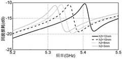
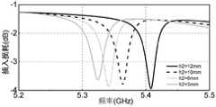
如图6所示,通过旋转第二调谐螺丝10,改变介质谐振器底部和介质基板的距离h2,可以改变本专利负群时延电路的中心频率和群时延的大小,当h1为1.2mm时,h2从12mm变化到3mm时,中心频率从5.408GHz减小到5.325GHz,且群时延从-4.6ns增加到-3.02ns,达到最大值。电路的回波损耗性能均小于-10dB,插入损耗均保持在-3dB至-4dB,且工作频带带宽大于20MHz.As shown in FIG. 6 , by rotating the
上述结果给出的是本专利的可调谐的大致范围,群时延值和中心频率均可在给出的范围中通过调节两个调谐螺丝来得到。The above results give the approximate tunable range of this patent, and the group delay value and the center frequency can be obtained by adjusting the two tuning screws within the given range.
综上所述,本发明所述的一种基于介质谐振器的非接触式可调负群时延电路实现了可调谐的负群时延特性,并且具有插入损耗小,端口匹配性好等特点,在5GHz的频段能获得较大的负群时延值,通过更换其他频率的介质谐振器还可以得到其他频段的负群时延电路,非常适合应用于各类射频微波通信系统中,解决通信系统中的时延问题。To sum up, the non-contact adjustable negative group delay circuit based on dielectric resonators of the present invention realizes the tunable negative group delay characteristics, and has the characteristics of small insertion loss and good port matching. , in the 5GHz frequency band, a large negative group delay value can be obtained. By replacing the dielectric resonators of other frequencies, the negative group delay circuits of other frequency bands can also be obtained. It is very suitable for application in various radio frequency microwave communication systems. Latency issues in the system.
虽然本发明已以较佳实施例揭露如上,然其并非用以限定本发明。本发明所属技术领域中具有通常知识者,在不脱离本发明的精神和范围内,当可作各种的更动与润饰。因此,本发明的保护范围当视权利要求书所界定者为准。Although the present invention has been disclosed above with preferred embodiments, it is not intended to limit the present invention. Those skilled in the art to which the present invention pertains can make various changes and modifications without departing from the spirit and scope of the present invention. Therefore, the protection scope of the present invention should be determined according to the claims.
Claims (7)
Translated fromChinese


Priority Applications (1)
| Application Number | Priority Date | Filing Date | Title |
|---|---|---|---|
| CN202111355973.3ACN114171871B (en) | 2021-11-16 | 2021-11-16 | Non-contact adjustable negative group delay circuit based on dielectric resonator and its construction method |
Applications Claiming Priority (1)
| Application Number | Priority Date | Filing Date | Title |
|---|---|---|---|
| CN202111355973.3ACN114171871B (en) | 2021-11-16 | 2021-11-16 | Non-contact adjustable negative group delay circuit based on dielectric resonator and its construction method |
Publications (2)
| Publication Number | Publication Date |
|---|---|
| CN114171871A CN114171871A (en) | 2022-03-11 |
| CN114171871Btrue CN114171871B (en) | 2022-09-02 |
Family
ID=80479206
Family Applications (1)
| Application Number | Title | Priority Date | Filing Date |
|---|---|---|---|
| CN202111355973.3AActiveCN114171871B (en) | 2021-11-16 | 2021-11-16 | Non-contact adjustable negative group delay circuit based on dielectric resonator and its construction method |
Country Status (1)
| Country | Link |
|---|---|
| CN (1) | CN114171871B (en) |
Families Citing this family (2)
| Publication number | Priority date | Publication date | Assignee | Title |
|---|---|---|---|---|
| CN114778954B (en)* | 2022-03-30 | 2025-06-20 | 南京信息工程大学 | A dielectric testing device and method based on microstrip negative group delay circuit |
| CN115133248B (en)* | 2022-05-12 | 2024-02-02 | 大连海事大学 | A broadband negative group delay microwave circuit based on stacked coupling patches |
Citations (2)
| Publication number | Priority date | Publication date | Assignee | Title |
|---|---|---|---|---|
| CN109560830A (en)* | 2018-11-20 | 2019-04-02 | 大连海事大学 | Self-matching negative group delay circuit with adjustable center frequency and adjustable group delay |
| CN109918864A (en)* | 2019-05-05 | 2019-06-21 | 南京信息工程大学 | Negative group delay circuit and design method based on sector stub and coupled microstrip line |
Family Cites Families (10)
| Publication number | Priority date | Publication date | Assignee | Title |
|---|---|---|---|---|
| US7274263B2 (en)* | 2004-08-25 | 2007-09-25 | Samsung Electronics Co., Ltd. | Microstrip stabilized quantum well resonance-tunneling generator for millimeter and submillimeter wavelength range |
| KR101026997B1 (en)* | 2009-03-09 | 2011-04-11 | 주식회사 이엠따블유 | Dual Band Stop Filter |
| JP6013793B2 (en)* | 2012-06-18 | 2016-10-25 | 日本電信電話株式会社 | Dispersion compensation medium |
| US9722589B1 (en)* | 2016-04-15 | 2017-08-01 | Microsoft Technology Licensing, Llc | Clock distribution network for a superconducting integrated circuit |
| CN107508572B (en)* | 2017-08-07 | 2021-01-15 | 大连海事大学 | Broadband negative group time delay microwave circuit based on distributed parameter realization |
| CN108566175B (en)* | 2018-03-26 | 2021-08-10 | 西南电子技术研究所(中国电子科技集团公司第十研究所) | Adjustable negative group delay circuit |
| JP7255143B2 (en)* | 2018-11-07 | 2023-04-11 | 富士通株式会社 | Group delay compensation filter |
| CN110378015B (en)* | 2019-07-17 | 2023-05-30 | 南京信息工程大学 | A Low Loss Negative Group Delay Circuit Based on Ring Microstrip Line |
| CN213690001U (en)* | 2020-10-12 | 2021-07-13 | 广东工业大学 | Waveguide structure of circular ring-shaped resonant cavity with notch |
| CN214153150U (en)* | 2021-02-09 | 2021-09-07 | 南京信息工程大学 | Crab-shaped double-frequency-band negative group time delay circuit |
- 2021
- 2021-11-16CNCN202111355973.3Apatent/CN114171871B/enactiveActive
Patent Citations (2)
| Publication number | Priority date | Publication date | Assignee | Title |
|---|---|---|---|---|
| CN109560830A (en)* | 2018-11-20 | 2019-04-02 | 大连海事大学 | Self-matching negative group delay circuit with adjustable center frequency and adjustable group delay |
| CN109918864A (en)* | 2019-05-05 | 2019-06-21 | 南京信息工程大学 | Negative group delay circuit and design method based on sector stub and coupled microstrip line |
Also Published As
| Publication number | Publication date |
|---|---|
| CN114171871A (en) | 2022-03-11 |
Similar Documents
| Publication | Publication Date | Title |
|---|---|---|
| CN108566175B (en) | Adjustable negative group delay circuit | |
| CN102403557B (en) | Highly Selective Dual Bandpass Filters with Independently Adjustable Passbands | |
| CN114171871B (en) | Non-contact adjustable negative group delay circuit based on dielectric resonator and its construction method | |
| CN105720339B (en) | Double-frequency adjustable band-pass filter | |
| US7432786B2 (en) | High frequency filter | |
| CN109524748B (en) | Frequency-tunable microstrip balance band-pass filter | |
| CN105552494B (en) | A kind of adjustable plane bandpass and band-rejection filter | |
| CN108493533B (en) | Tunable filter with stable wide stop band | |
| CN110459839B (en) | A Frequency Tunable Differential Double Pass Band Filter | |
| CN202373678U (en) | Miniaturized double-passband band-pass filter with adjustable low pass band | |
| CN113097670B (en) | Half-mode substrate integrated waveguide liquid crystal tunable filter with embedded coupling metal wire | |
| CN109473756B (en) | A Fully Reconfigurable Differential Filter | |
| CN104966871A (en) | Microstrip planar spiral filter and design method thereof | |
| CN111816962A (en) | A dielectric filter electromagnetic hybrid coupling structure and communication equipment | |
| CN202434677U (en) | High pass filter | |
| CN1945899A (en) | Micro strip antenna | |
| CN108923104B (en) | High-selectivity substrate integrated gap waveguide band-pass filter | |
| CN205646079U (en) | Adjustable plane band -pass - band elimination filter | |
| US20050206470A1 (en) | Lumped-element transmission line in multi-layered substrate | |
| CN109728388B (en) | A highly selective electrically adjustable coaxial filter with constant absolute bandwidth | |
| CN109687068B (en) | Broadband SIGW band-pass filter | |
| CN101777688A (en) | Microwave terminal short circuit half-wavelength tunable resonator and microwave tunable filter manufactured by same | |
| CN105789789A (en) | Tunable dual-band bandstop filter based on center loaded coupling structure | |
| US7142837B1 (en) | Multiple-section bandpass filter for broadcast communications | |
| CN211578932U (en) | T-type loaded dual-passband microstrip filter |
Legal Events
| Date | Code | Title | Description |
|---|---|---|---|
| PB01 | Publication | ||
| PB01 | Publication | ||
| SE01 | Entry into force of request for substantive examination | ||
| SE01 | Entry into force of request for substantive examination | ||
| GR01 | Patent grant | ||
| GR01 | Patent grant |