CN114070105A - Forward excitation constant current control device, switching power supply, control method and chip - Google Patents
Forward excitation constant current control device, switching power supply, control method and chipDownload PDFInfo
- Publication number
- CN114070105A CN114070105ACN202010786038.1ACN202010786038ACN114070105ACN 114070105 ACN114070105 ACN 114070105ACN 202010786038 ACN202010786038 ACN 202010786038ACN 114070105 ACN114070105 ACN 114070105A
- Authority
- CN
- China
- Prior art keywords
- signal
- circuit
- constant current
- current control
- constant
- Prior art date
- Legal status (The legal status is an assumption and is not a legal conclusion. Google has not performed a legal analysis and makes no representation as to the accuracy of the status listed.)
- Granted
Links
Images


Classifications
- H—ELECTRICITY
- H02—GENERATION; CONVERSION OR DISTRIBUTION OF ELECTRIC POWER
- H02M—APPARATUS FOR CONVERSION BETWEEN AC AND AC, BETWEEN AC AND DC, OR BETWEEN DC AND DC, AND FOR USE WITH MAINS OR SIMILAR POWER SUPPLY SYSTEMS; CONVERSION OF DC OR AC INPUT POWER INTO SURGE OUTPUT POWER; CONTROL OR REGULATION THEREOF
- H02M7/00—Conversion of AC power input into DC power output; Conversion of DC power input into AC power output
- H02M7/02—Conversion of AC power input into DC power output without possibility of reversal
- H02M7/04—Conversion of AC power input into DC power output without possibility of reversal by static converters
- H02M7/12—Conversion of AC power input into DC power output without possibility of reversal by static converters using discharge tubes with control electrode or semiconductor devices with control electrode
- H02M7/21—Conversion of AC power input into DC power output without possibility of reversal by static converters using discharge tubes with control electrode or semiconductor devices with control electrode using devices of a triode or transistor type requiring continuous application of a control signal
- H02M7/217—Conversion of AC power input into DC power output without possibility of reversal by static converters using discharge tubes with control electrode or semiconductor devices with control electrode using devices of a triode or transistor type requiring continuous application of a control signal using semiconductor devices only
- H—ELECTRICITY
- H02—GENERATION; CONVERSION OR DISTRIBUTION OF ELECTRIC POWER
- H02M—APPARATUS FOR CONVERSION BETWEEN AC AND AC, BETWEEN AC AND DC, OR BETWEEN DC AND DC, AND FOR USE WITH MAINS OR SIMILAR POWER SUPPLY SYSTEMS; CONVERSION OF DC OR AC INPUT POWER INTO SURGE OUTPUT POWER; CONTROL OR REGULATION THEREOF
- H02M3/00—Conversion of DC power input into DC power output
- H02M3/22—Conversion of DC power input into DC power output with intermediate conversion into AC
- H02M3/24—Conversion of DC power input into DC power output with intermediate conversion into AC by static converters
- H02M3/28—Conversion of DC power input into DC power output with intermediate conversion into AC by static converters using discharge tubes with control electrode or semiconductor devices with control electrode to produce the intermediate AC
- H02M3/325—Conversion of DC power input into DC power output with intermediate conversion into AC by static converters using discharge tubes with control electrode or semiconductor devices with control electrode to produce the intermediate AC using devices of a triode or a transistor type requiring continuous application of a control signal
- H02M3/335—Conversion of DC power input into DC power output with intermediate conversion into AC by static converters using discharge tubes with control electrode or semiconductor devices with control electrode to produce the intermediate AC using devices of a triode or a transistor type requiring continuous application of a control signal using semiconductor devices only
- H02M3/33507—Conversion of DC power input into DC power output with intermediate conversion into AC by static converters using discharge tubes with control electrode or semiconductor devices with control electrode to produce the intermediate AC using devices of a triode or a transistor type requiring continuous application of a control signal using semiconductor devices only with automatic control of the output voltage or current, e.g. flyback converters
- H02M3/33523—Conversion of DC power input into DC power output with intermediate conversion into AC by static converters using discharge tubes with control electrode or semiconductor devices with control electrode to produce the intermediate AC using devices of a triode or a transistor type requiring continuous application of a control signal using semiconductor devices only with automatic control of the output voltage or current, e.g. flyback converters with galvanic isolation between input and output of both the power stage and the feedback loop
- H—ELECTRICITY
- H05—ELECTRIC TECHNIQUES NOT OTHERWISE PROVIDED FOR
- H05B—ELECTRIC HEATING; ELECTRIC LIGHT SOURCES NOT OTHERWISE PROVIDED FOR; CIRCUIT ARRANGEMENTS FOR ELECTRIC LIGHT SOURCES, IN GENERAL
- H05B45/00—Circuit arrangements for operating light-emitting diodes [LED]
- H05B45/30—Driver circuits
- H05B45/345—Current stabilisation; Maintaining constant current
- Y—GENERAL TAGGING OF NEW TECHNOLOGICAL DEVELOPMENTS; GENERAL TAGGING OF CROSS-SECTIONAL TECHNOLOGIES SPANNING OVER SEVERAL SECTIONS OF THE IPC; TECHNICAL SUBJECTS COVERED BY FORMER USPC CROSS-REFERENCE ART COLLECTIONS [XRACs] AND DIGESTS
- Y02—TECHNOLOGIES OR APPLICATIONS FOR MITIGATION OR ADAPTATION AGAINST CLIMATE CHANGE
- Y02B—CLIMATE CHANGE MITIGATION TECHNOLOGIES RELATED TO BUILDINGS, e.g. HOUSING, HOUSE APPLIANCES OR RELATED END-USER APPLICATIONS
- Y02B20/00—Energy efficient lighting technologies, e.g. halogen lamps or gas discharge lamps
- Y02B20/30—Semiconductor lamps, e.g. solid state lamps [SSL] light emitting diodes [LED] or organic LED [OLED]
Landscapes
- Engineering & Computer Science (AREA)
- Power Engineering (AREA)
- Dc-Dc Converters (AREA)
Abstract
Description
Technical Field
The application relates to the technical field of control circuits, in particular to a forward constant current control device, a switching power supply, a control method and a chip.
Background
In order to match the power supply of various loads such as electronic terminals, displays, servers, various instruments and meters, the ac power provided by the power grid is generally converted into the dc power suitable for various loads by the switching power supply. Due to different power requirements of loads, a flyback structure is generally adopted as a direct current circuit of the switching power supply to be suitable for a low-power occasion, for example, an occasion with an output power level of 100W or less. In a high-power situation, for example, where the output power level requirement is 100W-300W, the flyback structure is no longer applicable due to the limitation of the duty ratio and the conversion efficiency of the transformer, and at this time, the switching power supply adopts the forward structure as its direct current converter circuit to achieve high-power output.
Although the forward switching power supply has a wide application in high-power occasions by virtue of the advantages of high conversion efficiency, simple topology, synchronous rectification and the like, the conventional forward switching power supply can only realize output constant voltage. Thus, the power supply device cannot be applied to loads such as a high-power LED panel which require constant current power supply.
Therefore, it is desirable to provide a forward constant current control device to enable a forward switching power supply to output a constant current.
Disclosure of Invention
In view of the above-mentioned drawbacks of the related art, an object of the present application is to provide a forward constant current control device, a switching power supply, a control method, and a chip.
To achieve the above and other related objects, a first aspect of the present application discloses a forward constant current control device for controlling a forward power circuit to perform energy conversion, comprising: the constant voltage control unit is used for outputting a constant voltage control signal based on the acquired feedback signal and the sampling signal when the load current is smaller than a preset constant current value; wherein the feedback signal reflects a load current of the forward power circuit, and the sampling signal reflects a peak current of the forward power circuit; the constant current control unit is used for outputting a constant current control signal based on the sampling signal when the load current reaches the preset constant current value; and the driving unit is coupled with the constant voltage control unit and the constant current control unit and used for driving the forward power circuit to output constant voltage power supply to a load or output constant current power supply to the load based on the constant voltage control signal or the constant current control signal.
In certain embodiments of the first aspect of the present application, the constant current control unit includes a first comparison circuit for comparing the sampling signal with a first reference signal to output the constant current control signal; wherein the first reference signal reflects the preset constant current value.
In certain embodiments of the first aspect of the present application, the constant voltage control unit includes a second comparison circuit for comparing the sampling signal and the feedback signal to output the constant voltage control signal during a period in which the feedback signal is smaller than the first reference signal.
In some embodiments of the first aspect of the present application, the driving unit is further configured to output a short-circuit protection signal to the driving unit to control the forward power circuit to implement short-circuit protection during a period when the load voltage is lower than a short-circuit protection threshold.
In certain embodiments of the first aspect of the present application, the short-circuit protection unit is further configured to maintain the short-circuit protection threshold stable based on the obtained rectified input signal.
In certain embodiments of the first aspect of the present application, the short-circuit protection unit comprises: the first time delay circuit is coupled with the constant current control unit and used for forbidding the constant current control unit when the conducting duration of the forward power circuit is lower than the reference duration; wherein the reference duration is associated with the short-circuit protection threshold; and the third comparison circuit is coupled to the driving unit and used for comparing the sampling signal with the second reference signal to output a comparison signal serving as the short-circuit protection signal to the driving unit.
In certain embodiments of the first aspect of the present application, the first delay circuit comprises: the first timing capacitor circuit comprises a timing capacitor and is used for executing timing operation; the first switch circuit is coupled to the first timing capacitor circuit and is used for disabling the constant current control unit when a voltage signal on one electrode side of the timing capacitor reaches a threshold voltage of the switch circuit.
In certain embodiments of the first aspect of the present application, the short-circuit protection unit further includes a compensation circuit, coupled to the first delay circuit, for compensating the reference duration based on a variation of the obtained rectified input signal to maintain the stability of the short-circuit protection threshold.
In certain embodiments of the first aspect of the present application, the compensation circuit changes the reference duration by changing a charging speed of a timing capacitor.
In certain embodiments of the first aspect of the present application, the short-circuit protection unit further comprises: and the timing circuit is coupled with the third comparison circuit and the driving unit and used for timing based on the comparison signal and outputting the short-circuit protection signal to the driving unit to control the forward constant current control device to stop working after timing is finished.
In certain embodiments of the first aspect of the present application, further comprising: and the duty ratio adjusting unit is coupled with the driving unit and used for outputting a duty ratio adjusting signal to the driving unit to control the forward power circuit to be switched off when the on duration of the forward power circuit exceeds a duration threshold.
In certain embodiments of the first aspect of the present application, the drive unit comprises: a PWM generating circuit for generating a PWM pulse signal; a logic circuit, coupled to the PWM generation circuit and at least one of the constant voltage control unit, the constant current control unit, the short-circuit protection unit, and the duty ratio adjustment unit, for outputting a logic signal based on at least one of the PWM pulse, the constant voltage control signal, the constant current control signal, the short-circuit protection signal, and the duty ratio adjustment signal; and the driving circuit is coupled to the logic circuit and used for controlling the forward power circuit to be switched on or switched off to perform energy conversion based on the logic signal.
A second aspect of the present application discloses a control chip, which is packaged with the forward constant current control device according to any one of the embodiments disclosed in the first aspect of the present application.
A third aspect of the present application discloses a forward constant current switching power supply, including: in certain embodiments of the second aspect of the present application, a rectifier circuit for receiving an external drive signal to output a rectified signal; the filter circuit is coupled to the rectifying circuit and used for filtering the rectifying signal to output a filtered signal; the forward constant current control device according to any one of the embodiments disclosed in the first aspect of the present application, configured to output a driving signal; the control end of the switching device is coupled with the forward constant current control device and used for switching on or off based on the driving signal; the forward power circuit is coupled with the switching device and used for performing energy conversion on the received input signal based on the on or off of the switching device so as to switch the output constant voltage into the output constant current when the load current reaches a preset constant current value; wherein the input signal is the filtered signal.
The third aspect of the present application discloses a forward constant current control method for controlling a forward power circuit to perform energy conversion, comprising the following steps: acquiring a feedback signal and a sampling signal; outputting a constant voltage control signal based on the feedback signal and the sampling signal during a period when the load current is less than a preset constant current value; wherein the feedback signal reflects a load current of the forward power circuit, and the sampling signal reflects a peak current of the forward power circuit; outputting a constant current control signal based on the sampling signal when the load current reaches the preset constant current value; and driving the forward power circuit to output constant voltage power supply to a load or output constant current power supply to the load based on the constant voltage control signal or the constant current control signal.
In certain embodiments of the third aspect of the present application, further comprising the steps of: and outputting a short-circuit protection signal to control the forward power circuit to realize short-circuit protection in a constant current stage when the load voltage is lower than a short-circuit protection threshold value.
In certain embodiments of the third aspect of the present application, further comprising the steps of: and when the on-time of the forward power circuit exceeds a preset time threshold, outputting a duty ratio adjusting signal to control the forward power circuit to be switched off.
In summary, the forward constant current control device, the system, the control method and the chip provided by the application can control the forward power circuit to switch from the output constant voltage to the output constant current when the load current exceeds the preset constant current value, and can be suitable for a high-power load with a constant current power supply requirement.
Drawings
The specific features of the invention to which this application relates are set forth in the appended claims. The features and advantages of the invention to which this application relates will be better understood by reference to the exemplary embodiments described in detail below and the accompanying drawings. The brief description of the drawings is as follows:
fig. 1 shows a block diagram of a constant current control circuit of a high-power LED load.
Fig. 2 is a schematic diagram illustrating an output power supply waveform of a forward power circuit under the control of a forward constant current control device according to an embodiment of the present disclosure.
Fig. 3 is a block diagram of an external circuit of the forward constant current control device according to an embodiment of the present disclosure.
Fig. 4 is a circuit block diagram of a forward constant current control device according to an embodiment of the present invention.
Fig. 5 is a circuit block diagram of the constant voltage control unit according to an embodiment of the present invention.
Fig. 6 is a circuit block diagram of a constant current control unit according to an embodiment of the present invention.
Fig. 7 is a circuit block diagram of a forward constant current control device according to another embodiment of the present application.
Fig. 8 is a waveform diagram illustrating a variation relationship between the energy storage and the load voltage of the forward power circuit according to an embodiment of the present invention.
Fig. 9 is a schematic diagram of an output power supply waveform of a forward power circuit under the control of a forward constant current control device according to another embodiment of the present application.
Fig. 10 is a circuit block diagram of the short-circuit protection unit according to an embodiment of the present invention.
Fig. 11 is a circuit structure diagram of a first delay circuit according to an embodiment of the present disclosure.
Fig. 12 is a circuit block diagram of the short-circuit protection unit according to another embodiment of the present application.
Fig. 13 is a schematic circuit diagram of a compensation circuit according to an embodiment of the present invention.
Fig. 14 is a circuit block diagram of a short-circuit protection unit according to another embodiment of the present application.
Fig. 15 is a block circuit diagram of the present application in a further embodiment.
Fig. 16 is a circuit block diagram of a duty cycle adjusting unit according to an embodiment of the present application.
Fig. 17 is a circuit diagram of a current converting circuit according to an embodiment of the present invention.
Fig. 18 is a circuit structure diagram of a second delay circuit according to an embodiment of the present application.
Fig. 19 is a waveform diagram illustrating a driving unit outputting logic signals based on various signals according to the present application.
Fig. 20 is a circuit block diagram of a driving unit according to an embodiment of the present application.
Fig. 21 is a circuit block diagram of a forward constant current switching power supply according to an embodiment of the present invention.
Detailed Description
The following description of the embodiments of the present application is provided for illustrative purposes, and other advantages and capabilities of the present application will become apparent to those skilled in the art from the present disclosure.
In the following description, reference is made to the accompanying drawings that describe several embodiments of the application. It is to be understood that other embodiments may be utilized and that mechanical, structural, electrical, and operational changes may be made without departing from the spirit and scope of the present disclosure. The following detailed description is not to be taken in a limiting sense, and the scope of embodiments of the present application is defined only by the claims of the issued patent. The terminology used herein is for the purpose of describing particular embodiments only and is not intended to be limiting of the application. Spatially relative terms, such as "upper," "lower," "left," "right," "lower," "below," "lower," "above," "upper," and the like, may be used herein to facilitate describing one element or feature's relationship to another element or feature as illustrated in the figures.
Although the terms first, second, etc. may be used herein to describe various elements or parameters in some instances, these elements or parameters should not be limited by these terms. These terms are only used to distinguish one element or parameter from another element or parameter. For example, a first delay circuit may be referred to as a second delay circuit, and similarly, a second delay circuit may be referred to as a first delay circuit, without departing from the scope of the various described embodiments. The first delay circuit and the second delay circuit are both described as one delay circuit, but they are not the same delay circuit unless the context clearly indicates otherwise. The first comparison circuit and the second comparison circuit, or the first timing capacitor circuit and the second timing capacitor circuit, or the first switch circuit and the second switch circuit are also included in the similar situation.
Also, as used herein, the singular forms "a", "an" and "the" are intended to include the plural forms as well, unless the context indicates otherwise. It will be further understood that the terms "comprises," "comprising," "includes" and/or "including," when used in this specification, specify the presence of stated features, steps, operations, elements, components, items, species, and/or groups, but do not preclude the presence, or addition of one or more other features, steps, operations, elements, components, species, and/or groups thereof. The terms "or" and/or "as used herein are to be construed as inclusive or meaning any one or any combination. Thus, "A, B or C" or "A, B and/or C" means "any of the following: a; b; c; a and B; a and C; b and C; A. b and C ". An exception to this definition will occur only when a combination of elements, functions, steps or operations are inherently mutually exclusive in some way.
In addition, it should be noted that the present disclosure is described below in terms of various embodiments in order to clearly illustrate various inventive features disclosed herein. But not to mean that the various embodiments can only be practiced individually. One skilled in the art may design the available embodiments according to the requirements, or only replaceable components/modules in different embodiments may be replaced according to the design requirements. In other words, the embodiments taught by the present disclosure are not limited to the aspects described in the following embodiments, but include substitutions and permutations and combinations of various embodiments/components/modules as may be made herein before.
The flyback switching power supply is suitable for a small power situation with an output power level of less than 100W, on one hand, the duty ratio of the flyback switching power supply is generally limited to be less than 0.5 in order to prevent overvoltage breakdown of a switching device in the flyback switching power supply, and the current flowing through the flyback switching power supply generally presents a Discontinuous Mode (DCM), and on the other hand, the flyback switching power supply has a large leakage inductance of a primary coil and a secondary coil of a transformer, and the conversion efficiency is low.
The energy storage inductor of the forward switching power supply provides output to the load during the period of controlling the switching device to be switched on and off, so that the load capacity of the forward switching power supply is relatively strong, the forward switching power supply is suitable for occasions with high power (such as 100W-300W), and under the condition of heavy load, the current flowing through the energy storage inductor of the forward switching power supply is in a Continuous Mode (CCM). The heavy load refers to a load factor of the switching power supply being too high, for example, the load factor is 80% to 95%, for a forward switching power supply, the forward switching power supply generally operates under the heavy load, but it should be noted that the load factor is only a relative comparative value between 80% and 95%, and is not understood as a strict definition of the heavy load, and a specific range of the load factor of the heavy load may be newly defined.
However, in practical applications, the forward switching power supply generally adopts a constant voltage output mode to supply power to the load, and the load current of the forward switching power supply changes along with the impedance change of the load, so that the load which has a requirement for constant current power supply cannot be satisfied. For example, for a high-power LED load, the cost is high, and when the high-power LED load operates in a constant-voltage power supply mode, on one hand, the current flowing through the high-power LED load continuously increases with temperature rise, and on the other hand, according to the current-voltage characteristic curve of the LED load, a slight change in voltage may cause a rapid change in current, so that the high-power LED load is easily over-current, thereby affecting the lifetime and even burning out directly.
In order to avoid damage caused by the fact that the current flowing through the high-power LED load exceeds the maximum value, the LED load is expected to operate in a constant current mode, please refer to fig. 1, which shows a constant current control circuit block diagram of the high-power LED load, as shown in fig. 1, a forwardswitching power supply 10 outputting a constant voltage is generally used as a constant voltage power supply, and a constantcurrent module 11 is externally provided to realize constant current power supply to the LED load, wherein the forwardswitching power supply 10 is used for converting an external alternating current signal AC into a direct current constant voltage and outputting the direct current constant voltage to the constantcurrent module 11 to convert the direct current constant voltage into a constant current and outputting the constant current to the LED load for power supply.
However, the constant current control circuit shown in fig. 1 has a complicated structure, and for a user, a professional is required to match a corresponding constantcurrent module 11 with a forwardswitching power supply 10 that outputs constant voltage power supply and complete circuit construction, and for the circuit structure shown in fig. 1, on one hand, secondary conversion of electric energy is required, and the conversion efficiency and the working stability are not good enough, and on the other hand, the circuit structure can only work in one mode of outputting constant current, and cannot be adapted to the change of load between outputting constant voltage power supply and outputting constant current power supply.
In view of the above, the present application provides a forward constant current control device, configured to control a forward power circuit to perform energy conversion, so that when a load current reaches a preset constant current value, the forward power circuit is switched from an output constant voltage power supply mode to an output constant current power supply mode. Please refer to fig. 2, which is a schematic diagram illustrating a waveform of power supplied by an output of a forward power circuit under the control of a forward constant current control device in an embodiment of the present application, where as shown in the diagram, the preset constant current value Io is a load current value of the forward power circuit entering an output constant current stage, and in a range where the load current I of the forward power circuit is smaller than the preset constant current value Io, an external high-power LED load is not damaged due to an increase of the load current, and the forward constant current control device may control the forward power circuit to operate in an output constant voltage power supply mode (I < Io in fig. 2, corresponding to a V ═ Vo waveform); after the load current I of the forward power circuit reaches the preset constant current value Io, if the load current I of the forward power circuit continues to increase, the problem of damage to the high-power LED load may be caused, and therefore, once the load current I of the forward power circuit reaches the preset constant current value Io, the forward constant current control device controls the forward power circuit to operate in an output constant current power supply mode (in a waveform at a stage of I > Io in fig. 2) so that the load current I of the forward power circuit is basically maintained unchanged. It should be noted that, because the constant current mode of the forward power circuit is affected by the load voltage, the maintained preset constant current value Io is not completely unchanged, and has a waveform as shown in the stage I > Io in fig. 2, the load current of the forward power circuit slightly increases with the decrease of the load voltage V, but because the maximum increment of the load current can meet the current precision requirement of the constant current mode, the current slight change in the constant current stage is regarded as being maintained at the preset constant current value Io unless otherwise specified in the present application.
It should be noted that the forward constant-current control device provided in the present application controls the forward power circuit to output a constant-voltage power supply to the load or output a constant-current power supply to the load in a Pulse Width Modulation (PWM) manner, that is, in the entire control process of the forward power circuit in the present application, the on-off period of the forward power circuit is not changed (that is, the on-off period is the period of the PWM Pulse signal output by the Pulse width modulation), and the forward constant-current control device controls the forward power circuit to output the constant-voltage power supply or output the constant-current power supply by changing the duty ratio of the forward power circuit. The current of the energy storage inductor is in a continuous mode under the heavy load condition, so that the forward constant current control device achieves the purpose of changing the duty ratio of the forward power circuit by changing the on-time or the turn-off time of the forward power circuit, and the adjustment of the on-time or the turn-off time of the forward power circuit mentioned later can be understood as the adjustment of the duty ratio.
In addition, the forward constant current control device of the present application controls the forward power circuit to achieve the above-mentioned functions by controlling the on and off of a switching device coupled to the forward power circuit, as shown in fig. 3, fig. 3 is a block diagram of an external circuit of the forward constant current control device of the present application in one embodiment, the switchingdevice 50 is a three-terminal controllable device, the three-terminal controllable device includes a control terminal, a first terminal, and a second terminal, the first terminal is coupled to theforward power circuit 40, the second terminal is grounded GND, the control terminal controls the forward constantcurrent control device 20 to turn on or off the first terminal and the second terminal, so that theforward power circuit 40 performs energy conversion on the received input signal Vin to supply power to the load output load Vout, wherein the load power Vout is constant voltage power supply or constant current power supply, the input signal Vin is an electrical signal output after an external alternating current electrical signal is rectified. In this application, just swashing constant current controlling means control when switching device switches on, think control promptly just the power circuit that just is just swashing switches on, just is just that the power circuit that just is swashing is in the excitation stage, just swashing constant current controlling means control when switching device switches off, think control promptly just the power circuit that just is swashing cuts off, just it is in the demagnetization stage also to be just swashing power circuit, switching device's on-off cycle thinks the on-off cycle of just swashing power circuit promptly. The aforementioned and the later mentioned control of the switching on and off of the forward power circuit is understood without particular reference.
Wherein, due to different dividing modes of circuit modules, in some embodiments, the switch device can be used as a part of the forward power circuit. In other embodiments, the switching device may be included as a part of a forward constant current control apparatus, and the application is not limited thereto. In a specific embodiment, the switching device includes a controllable Transistor, which may be, for example, a Metal-oxide-semiconductor Field-effect Transistor (MOSFET) or a Bipolar Junction Transistor (BJT).
Referring to fig. 4, which is a circuit block diagram of the forward constant current control device in an embodiment of the present application, as shown in the figure, the forward constantcurrent control device 20 includes a constantvoltage control unit 21, a constantcurrent control unit 22, and a drivingunit 23. The constantvoltage control unit 21 has a first input terminal P _211, a second input terminal P _212, and an output terminal P _213, the first input terminal P _211 is configured to be coupled to the forward power circuit to obtain a sampling signal Cs reflecting a peak current of the forward power circuit, the second input terminal P _212 is configured to be coupled to the forward power circuit to obtain a feedback signal Fb reflecting a load current of the forward power circuit, and the constantvoltage control unit 21 outputs a constant voltage control signal Cv through the output terminal P _213 based on the feedback signal Fb and the sampling signal Cs during a period when the load current is smaller than a preset constant current value. The constantcurrent control unit 22 has an input end P _221 and an output end P _222, the input end P _221 obtains the sampling signal Cs, and the constantcurrent control unit 22 outputs a constant current control signal Cc through the output end P _222 based on the sampling signal Cs when the load current reaches a preset constant current value. The driving unit is coupled to the first input terminal P _211 and the input terminal P _221, and is configured to drive the forward power circuit to output constant voltage power to the load or output constant current power to the load based on the constant voltage control signal Cv or the constant current control signal Cc.
The preset constant current value is reflected by a first reference signal arranged inside the forward constantcurrent control device 20, the constantvoltage control unit 21 works when the feedback signal Fb does not reach the first reference signal (that is, the load current of the forward power circuit does not reach the preset constant current value), and the forward power circuit works in the output constant voltage power supply mode by comparing the sampling signal Cs with the feedback signal Fb. The constantcurrent control unit 22 operates during a period in which the feedback signal Fb is greater than the first reference signal (i.e., the load current of the forward power circuit reaches a preset constant current value), and compares the sampling signal Cs with the first reference signal to enable the forward power circuit to operate in an output constant current power supply mode. In an embodiment, the first reference signal may be, for example, a reference voltage signal generated by a power supply of the forward constantcurrent control device 20, and may also be, for example, a voltage signal provided by a constant voltage source, which is not limited in this application.
In an embodiment, please refer to fig. 5, which is a circuit block diagram of the constant voltage control unit in an embodiment of the present application, as shown in the figure, the constantvoltage control unit 21 includes a second comparingcircuit 211, one input terminal of the second comparingcircuit 211 is used for connecting to the first input terminal P _211 to obtain the sampling signal Cs, the other input terminal thereof is used for connecting to the second input terminal P _212 to obtain the feedback signal Fb, and the output terminal thereof is used as the output terminal P _213 of the constantvoltage control unit 21 to output the constant voltage control signal Cv when the second comparingcircuit 221 determines that the sampling signal Cs reaches the feedback signal Fb through comparison. In other words, in the present embodiment, the feedback signal Fb reflects the load current of the forward power circuit, and the larger the load current of the forward power circuit is, the larger the feedback signal Fb is, and the feedback signal Fb determines the peak value of the peak current of the stable forward power circuit for maintaining the load voltage of the forward power circuit in each on-off period during which the feedback signal Fb does not reach the first reference signal, so that the constantvoltage control unit 21 outputs the constant voltage control signal Cv to enable the driving unit to control the turn-off of the forward power circuit based on the constant voltage control signal Cv when determining that the peak current of the forward power circuit reaches the peak value to be reached by maintaining the voltage to be constant by sampling the signal Cs and the feedback signal Fb in one on-off period.
In an embodiment, please refer to fig. 6, which is a circuit block diagram of the constant current control unit in an embodiment of the present application, as shown in the figure, the constantcurrent control unit 22 includes afirst comparison circuit 221, one input terminal of thefirst comparison circuit 221 is used for being connected to the input terminal P _221 of the constantcurrent control unit 22 to obtain the sampling signal Cs, the other input terminal of thefirst comparison circuit 221 is used for obtaining the first reference signal Vref1, and the output terminal of the first comparison circuit is used as the output terminal P _222 of the constantcurrent control unit 22 to output the constant current control signal Cc when thefirst comparison circuit 221 determines that the sampling signal Cs reaches the first reference signal Vref1 through comparison. In other words, in the present embodiment, the first reference signal Vref1 is set to a fixed value, which determines that the peak value of the peak current of the forward power circuit is fixed in order to maintain the load current of the forward power circuit stable at a preset constant current value, that is, in each on-off period during which the feedback signal Fb is greater than the first reference signal Vref1, the peak value of the peak current is fixed and unchanged in order to maintain the load current stable, so that the constantcurrent control unit 22 outputs the constant current control signal Cc to enable the driving unit to control the forward power circuit to be turned off based on the constant current control signal Cc when determining that the peak current of the forward power circuit reaches the fixed value that the load current should be maintained to be constant through the sampling signal Cs and the first reference signal Vref1 in one on-off period.
How the constant voltage control unit and the constant current control unit operate in coordination is described below with reference to fig. 5 and 6. Taking an on-off period of the forward power circuit as an example, during the on period of the forward power circuit, the peak current of the forward power circuit increases with the increase of time, that is, the sampling signals Cs obtained by the constantvoltage control unit 21 and the constantcurrent control unit 22 increase. If the load current of the forward power circuit is smaller than the preset constant current value, that is, the feedback signal Fb is smaller than the first reference signal Vref1, at this time, once the sampling signal Cs reaches the feedback signal Fb, the constantvoltage control unit 21 outputs the constant voltage control signal Cv first to enable the driving unit to control the forward power circuit to be turned off, that is, during the period that the feedback signal Fb is smaller than the first reference signal Vref1, the sampling signal Cs does not reach the first reference signal Vref1, so that the constantcurrent control unit 22 stops at this stage. If the load current of the forward power circuit increases to the preset constant current value, that is, the feedback signal Fb is greater than the first reference signal Vref1, at this time, once the sampling signal Cs reaches the first reference signal Vref1, the constantcurrent control unit 22 first outputs the constant current control signal Cc to enable the driving unit to control the forward power circuit to be turned off, that is, at this stage, the sampling signal Cs does not have a chance to reach the feedback signal Fb, so that the constantvoltage control unit 21 stops at this stage.
As can be seen from the foregoing, in the stage of the forward power circuit outputting the constant current for power supply, the load current is stabilized at the preset constant current value, so that the load voltage changes with the change of the load resistance, and if the load voltage is too low, the load resistance is too small, and at this time, the load is still maintained at the preset constant current value and exceeds the maximum current value that the load can bear, thereby damaging the load.
In view of this, referring to fig. 7, a circuit block diagram of the forward constant current control device in another embodiment of the present invention is shown, as shown in the figure, in this embodiment, the forward constant current control device further includes a short-circuit protection unit 24, coupled to the drivingunit 23 through an output end P _243 thereof, for outputting a short-circuit protection signal Pro to the drivingunit 23 during a period when a load voltage is lower than a short-circuit protection threshold value to control the forward power circuit to implement short-circuit protection in a stage of outputting a constant current.
In the present application, for a forward power circuit, the current of the energy storage inductor of the forward power circuit presents a continuous mode. Therefore, referring to fig. 8, a waveform diagram of a variation relationship between the energy storage and the load voltage of the forward power circuit according to an embodiment of the present invention is shown, as shown in the constant current stage, as the load voltage of the forward power circuit decreases, the peak value Ipkc that the peak current of the forward power circuit should reach is maintained (see the above description for fig. 6), but the initial current Ipk increases and the on-time Ton decreases when the forward power circuit is turned on (as shown in the curves V1 and V2 in fig. 8, the load voltage represented by the curve V1 is greater than the curve V2, and Ton2< Ton 1). Therefore, in view of the relationship between the load voltage and the on-time of the forward power circuit, the forward constant current control device of the present application may determine the reference time length Tonleb corresponding to the short-circuit protection threshold in advance, so that the short-circuit protection unit 24 determines whether the load voltage is lower than the short-circuit protection threshold by determining whether the on-time length Ton is lower than the reference time length Tonleb. Meanwhile, in order to avoid that the forward constant current control device controls the forward power circuit to work in a constant voltage stage to generate error protection, so that the forward constant current control device cannot control the forward power circuit to work normally, when the short-circuit protection unit 24 judges that the on-time Ton is lower than the reference time Ton, the forward power circuit is not maintained in the constant current stage, at this time, the peak value Ipkc which the peak current of the forward power circuit should reach is not fixed any more, and changes in an opposite relation with the on-time Ton (in a Ton stage as shown in fig. 8). Therefore, further, the short-circuit protection unit 24 outputs the short-circuit protection signal Pro by detecting the sampling signal Cs reflecting the peak current of the forward power circuit and upon judging that the sampling signal Cs reaches the second reference signal Vref 2. The second reference signal Vref2 reflects a peak value Ipkcmax corresponding to a time point selected in the Tonleb stage in fig. 8 (the selected time point should be close to the reference duration Tonleb), and the second reference signal Vref2 is greater than the firstreference signal Vref 1.
Referring to fig. 9, a schematic diagram of a power supply waveform output by the forward power circuit under the control of the forward constant current control device in another embodiment of the present application is shown, as shown in fig. 2, on the basis of the waveform shown in fig. 2, when the load voltage of the forward power circuit drops to the short-circuit protection threshold Vpro in the constant current stage, under the control of the short-circuit protection unit of the forward constant current control device, the forward power circuit is turned off after the load current thereof suddenly increases (corresponding to a control process of the short-circuit protection unit outputting the short-circuit protection signal Pro when the short-circuit protection unit determines that the sampling signal Cs reaches the second reference signal Vref 2). It should be noted that, under the control of the short-circuit protection unit, the forward power circuit is not turned off immediately after the load voltage drops to the short-circuit protection threshold Vpro, so the short-circuit protection point actually realized by the short-circuit protection unit is slightly smaller than the short-circuit protection threshold Vmin, as shown in fig. 9, when the load voltage is Vpro. Since the difference between the two is small, the short-circuit protection threshold Vpro is described as a short-circuit protection point for the short-circuit protection unit 24 to implement short-circuit protection.
Referring to fig. 10, which is a circuit block diagram of the short-circuit protection unit according to an embodiment of the present invention, as shown, the short-circuit protection unit 24 includes afirst delay circuit 241 and athird comparison circuit 242. The output end P _246 of thefirst delay circuit 241 is coupled to the constant current control unit (not shown in fig. 10) for disabling the constant current control unit when the on-time Ton of the forward power circuit is lower than the reference time Ton. One input terminal P _241 of the third comparingcircuit 242 is used for obtaining the sampling signal Cs, the other input terminal P _242 is used for obtaining a second reference signal Vref2, and an output terminal thereof is used as an output terminal P _243 of the short-circuit protection unit 24 to be coupled to the driving unit, so as to output a comparison signal as a short-circuit protection signal Pro to the driving unit when the third comparingcircuit 242 determines through comparison that the sampling signal Cs reaches the second reference signal Vref2, so that the driving unit controls the forward constant current control device to stop operating based on the short-circuit protection signal Pro.
Referring to fig. 11, which is a schematic circuit diagram of a first delay circuit according to an embodiment of the present disclosure, as shown in the figure, thefirst delay circuit 241 includes a firsttiming capacitor circuit 2411 and afirst switch circuit 2412. The firsttiming capacitor circuit 2411 includes an input terminal P _244 and an output terminal P _245, and includes a not gate Ng1, switching transistors N1 and P1, and a timing capacitor C1. The input of the not gate Ng1 is used as the input terminal P _244 of the first timing capacitor circuit, the control terminals of the switch tube N1 and the switch tube P1 are coupled to the output of the not gate Ng1 after being connected, the first terminal of the switch tube P1 is coupled to the power supply Vcc via the current source Ib1, the second terminal of the switch tube N1 is grounded Gnd, the second terminal of the switch tube P1 and the first terminal of the switch tube N1 are connected to one terminal of the timing capacitor C1, one terminal of the timing capacitor C1 is further connected to the output terminal P _245, and the other terminal of the timing capacitor C1 is grounded Gnd. Thefirst switch circuit 2412 includes a switch tube P2 and a latch D1, the control terminal of the switch tube P2 is connected to the output terminal P _245, the first terminal thereof is coupled to the power supply Vcc, the second terminal thereof is connected to the ground Gnd via the current source Ib2, the second terminal thereof is further coupled to one terminal of the latch D1, and the other terminal of the latch D1 is connected to the output terminal P _246 of thefirst delay circuit 241 for serving as the output of thefirst delay circuit 241.
The input end P _244 of the firsttiming capacitor circuit 2411 is configured to be coupled to the driving unit to receive a logic signal Log output by the driving unit, so that the timing capacitor C1 performs a timing operation based on the logic signal Log, where the logic signal Log can reflect the on and off durations of the forward power circuit, and the working principle of the driving unit outputting the logic signal Log is described in detail later, and is not expanded here. Thefirst switch circuit 2412 outputs an disable signal Uable through the output terminal P _246 to disable the constant current control unit when the voltage signal of one electrode side of the timing capacitor C1 reaches its threshold voltage.
The operation of thefirst delay circuit 241 in the embodiment shown in fig. 11 is explained below. Taking the example that the switch tube N1 in fig. 11 is an N-type MOSFET, and the switch tubes P1 and P2 are P-type MOSFETs, in an on-off period T of the forward power circuit, at the off stage of the forward power circuit, the logic signal Log is at a low level, and becomes a high level after passing through the nor gate Ng2, the switch tube P1 is turned off, the switch tube N1 is turned on, and the charging capacitor C1 is discharged through the switch tube N1. In the conducting stage of the forward power circuit, the logic signal Log is at a high level and changes to a low level after passing through the nor gate Ng1, the switch tube P1 is turned on, the switch tube N1 is turned off, and the power supply Vcc takes the current value of the current source Ib1 as a charging current to charge the charging capacitor C1 through the switch tube P1. If the on-time of the forward power circuit exceeds the reference time Tonleb (i.e. the load voltage is higher than the short-circuit protection threshold), the voltage signal of the end of the charging capacitor C1 connected to the output end P _245 is at a threshold voltage higher than that corresponding to the off point of the switching tube P2, so that the switching tube P2 is in an off state, and the low level output by the second end of the switching tube P2 can trigger the latch D1 to output the disable signal Uable. If the on-time of the forward power circuit does not exceed the reference time Tonleb (i.e. the load voltage is lower than the short-circuit protection threshold), the voltage signal at the end of the charging capacitor C1 connected to the output end P _245 does not exceed the threshold voltage corresponding to the off-point of the switch tube P2, so that the switch tube P2 is turned on, the second end of the switch tube P2 becomes high level, and the latch D1 latches the high level to output the disable signal Uable. The current value of the current source Ib1 determines the charging speed C1 of the charging capacitor, and under the condition that the threshold voltage of the switching tube P2 is not changed, a person skilled in the art can set the reference time length Tonleb by selecting an appropriate current source Ib1 according to requirements.
It should be noted that the circuit structure of thefirst delay circuit 241 shown in fig. 11 is only an example, in other embodiments, the types and connection modes of the switch tubes in the firsttiming capacitor circuit 2411 shown in fig. 11 can be flexibly selected according to actual situations and matched with additional electronic components according to requirements, the principle of which is similar to that shown in fig. 11, and the intended function of fig. 11 is not affected. The switch P2 in the first switch circuit 2422 in fig. 11 can be replaced by other types or other devices and flexibly select logic devices to be collocated according to the replaced devices to achieve the above functions, for example, the first switch circuit 2422 can include a comparator and a latch, one input terminal of the comparator is coupled to one end of the timing capacitor C1, the other input terminal is used for obtaining a reference voltage (which can be a voltage signal generated by the power supply Vcc and whose magnitude can be, for example, equal to the threshold voltage of the switch P2, and can be specifically set according to practice), when one end of the timing capacitor C1 is determined to be dropped to the reference voltage obtained by the comparator through comparison, the comparator outputs a high level to the latch, so that the latch latches the high level to output the disable signal Uable. The first delay circuit of the present application is not limited to the circuit structure shown in fig. 11, and it is within the scope covered by the first delay circuit of the present application as long as the timing of the on or off duration of the forward power circuit based on the charging and discharging of the timing capacitor can be completed to output the disable signal.
The operation principle of the short-circuit protection unit 24 in an embodiment of the present application is described below with reference to fig. 10, 5, 6, and 7 according to the operation principle of thefirst delay circuit 241 shown in fig. 11, where, in the constant voltage phase, the load current is small, i.e., the feedback signal Fb is smaller than the first reference signal Vref1 and the second reference signal Vref2, at this time, once the sampling signal Cs reaches the feedback signal Fb, the constantvoltage control unit 21 outputs the constant voltage control signal Cv first to make the driving unit control the forward power circuit to turn off, i.e., the sampling signal Cs does not reach the first reference signal Vref1 or the second reference signal Vref2 at the constant voltage stage, so that the constantcurrent control unit 22 and the shortcircuit protection unit 24 are at rest at this stage, even if thefirst delay circuit 241 in the short-circuit protection unit 24 detects that the on-time of the forward power circuit is lower than the reference time Tonleb, thethird comparison circuit 242 in the short-circuit protection unit 24 cannot be caused to output the short-circuit protection signal Pro. In the constant current stage, since the load current is large, the feedback signal Fb is greater than the first reference signal Vref1 and the second reference signal Vref2, the constantvoltage control unit 21 is inactive, when thefirst delay circuit 241 of the short-circuit protection unit 24 determines that the on-time of the forward power circuit is lower than the reference time Tonleb (the load voltage is lower than the short-circuit protection threshold), the disable signal Uable is output, the constantcurrent control unit 22 disables based on the disable signal Uable, the magnitude of the sampling signal Cs and the first reference signal Vref1 are not compared any more, and the magnitudes of the sampled signal Cs and the second reference signal Vref2 are compared by thethird comparison circuit 242 of the short-circuit protection unit 24, when the sampling signal Cs reaches the second reference signal Vref2, the comparison signal is output as a short-circuit protection signal Pro, thedrive unit 23 turns off the forward power circuit based on the short-circuit protection signal Pro, therefore, short-circuit protection is realized in the constant current stage, and the forward constant current control device can not be influenced to control the forward power circuit to work in the constant voltage stage.
As can be seen from the description of fig. 3, for the forward power circuit, the energy conversion is performed on the input signal Vin under the control of the forward constant current control device to realize the power supply of the output load, and the power supply of the load output by the forward power circuit is not only related to the turn-off timing (i.e. duty ratio) of the forward power circuit controlled by the forward constant current control device, but also related to the input signal Vin. When the input signal Vin changes, if the short-circuit protection unit 24 still compares the on-time of the forward power circuit with the set fixed reference time Tonleb to output the short-circuit protection signal, the short-circuit protection signal is output according to the formula Wherein Vpro is a short-circuit protection threshold, N is an original secondary side turn ratio of a transformer in the forward power circuit, and it can be known that an actually achieved short-circuit protection point is not an expected short-circuit protection threshold. For example, in the absence of considerationIn a case where the input signal Vin is changed (for example, Vin is 230V), the set reference time duration Tonleb is 0.3ms, and the short-circuit protection point reached by the short-
circuit protection unit 24 is the expected short-circuit protection threshold 2.5V, that is, the short-circuit protection is triggered when the load voltage is actually lower than 2.5V. However, once the input signal Vin fluctuates or changes (for example, Vin is 250V), the short-circuit protection unit 24 still uses the reference time length Tonleb is 0.3ms as a criterion for determining whether the load voltage is lower than 2.5V, the short-circuit protection point reached by the short-circuit protection unit 24 is actually 3V, that is, the load voltage triggers short-circuit protection already when lower than 3V, or the input signal Vin becomes smaller (for example, Vin is 210V), the short-circuit protection point reached by the short-circuit protection unit 24 is actually 2V, that is, the load voltage starts to trigger short-circuit protection only when lower than 2V, and it is not favorable for the load whether to trigger the short-circuit protection early or too late.

In view of the above, in another embodiment, the short-circuit protection unit 24 is further configured to obtain the input signal Vin to maintain the stability of the short-circuit protection threshold value based on the input signal Vin. As shown in fig. 12, fig. 12 is a circuit block diagram of the short-circuit protection unit in another embodiment of the present application, and as shown in the figure, the short-circuit protection unit 24 further includes acompensation circuit 243 based on the circuit architecture shown in fig. 10, thecompensation circuit 243 obtains the input signal Vin through an input end P _247 thereof, and is coupled to the first delay circuit (not shown in fig. 12) through an output end P _248 thereof, and thecompensation circuit 243 compensates the reference time length based on a change of the input signal Vin to maintain a stable short-circuit protection threshold. In particular, also according to the conversion formula of the forward power circuit When the input signal Vin changes, the reference time duration Tonleb may be changed according to an inverse transformation rule, and when the input signal Vin increases, the reference time duration Tonleb is decreased, and when the input signal Vin decreases, the reference time duration Tonleb is increased.

Referring to fig. 13, which is a schematic circuit diagram of the compensation circuit of the present application in an embodiment, as shown in the figure, thecompensation circuit 243 includes a resistor R1, a first pair of switching transistors (N2, N3), and a second pair of switching transistors (P3, P4). One end of the resistor R1 is coupled to the input terminal P _247 of thecompensation circuit 243, and the other end is coupled to the first end of the first pair of switching tubes (N2, N3). The second end of the first pair of switching tubes (N2, N3) is grounded Gnd, and the third end is coupled with the first end of the second pair of switching tubes (P3, P4). The second end of the second pair of switching tubes (P3, P4) is coupled to the power supply Vcc, and the third end is coupled to the output end P _248 of thecompensation circuit 243. The resistor R1 is used for sampling the input signal Vin, and the first pair of switching transistors (N2, N3) and the second pair of switching transistors (P3, P4) are coupled to form a current mirror circuit so as to output a charging current Ib3 to the first delay circuit at the output terminal P _248 of thecompensation circuit 243 based on the sampling of the resistor R1. That is, the current value of charge current Ib3 has the same trend of change as input signal Vin, and as input signal Vin becomes larger, the current value of charge current Ib3 increases, and as input signal Vin becomes smaller, the current value of charge current Ib3 decreases. In practical applications, the charging current Ib3 is output to the timing capacitor in thefirst delay circuit 241, so that the timing capacitor is charged with the charging current Ib3, and when the input signal Vin changes, the reference time duration is changed by changing the charging speed of the timing capacitor, so as to achieve the purpose of maintaining the stability of the short-circuit protection threshold of the short-circuit protection unit 24.
Further, when thefirst delay circuit 241 adopts the circuit structure shown in fig. 11, the output terminal P _248 of thecompensation circuit 243 shown in fig. 13 is coupled to the first terminal of the switching tube P2 shown in fig. 11. However, it should be noted that, in order to simplify the circuit connection and facilitate the adjustment, when thefirst delay circuit 241 shown in fig. 11 is coupled to thecompensation circuit 243 shown in fig. 13, the first terminal of the switch tube P2 in fig. 11 is not necessarily coupled to the power supply Vcc via thecurrent source Ib 1.
With reference to fig. 13 and fig. 11, it is described how the short-circuit protection unit 24 changes the reference time length Tonleb to maintain the stability of the short-circuit protection threshold, the current value of the charging current Ib3 output by the compensation circuit 243 follows the change of the input signal Vin, when the input signal Vin becomes larger, the charging current Ib3 also increases, the first timing capacitor circuit 2411 charges the timing capacitor C1 with the charging current Ib3 during the turn-off period of the forward power circuit, and as the charging speed increases, the time length for which the voltage signal at one end of the timing capacitor C1 becomes the threshold voltage corresponding to the turn-off point of the switching tube P2 decreases, and then the reference time length Tonleb decreases, so that Vin in the above formula is not changed, and the short-circuit protection threshold is still the corresponding short-circuit protection threshold before the input signal Vin does not increase; when the input signal Vin is decreased, the charging current Ib3 is also decreased, the first timing capacitor circuit 2411 charges the timing capacitor C1 with the charging current Ib3 during the turn-off period of the forward power circuit, and as the charging speed is decreased, the duration that the voltage signal at one end of the timing capacitor C1 becomes the threshold voltage corresponding to the turn-off point of the switching tube P2 is increased, and the reference duration Tonleb is increased, so that Vin × Tonleb in the above formula is not changed, and the short-circuit protection threshold is still the corresponding short-circuit protection threshold before the input signal Vin is not decreased.
It should be noted that, when an interference test such as EFT (Electrical Fast Transient/burst), a lightning stroke, etc. is performed, a peak current flowing through the forward power circuit may be instantaneously increased to the second reference signal Vref2, so that the third comparingcircuit 242 outputs a comparison signal, and if the comparison signal is used as the short-circuit protection signal Pro to the driving unit, the driving unit controls the forward constant current control device to stop working, so that the short-circuit protection function is triggered by mistake. To avoid the false triggering of the short-circuit protection unit caused by these disturbances, as shown in fig. 14, it is shown as a circuit block diagram of the short-circuit protection unit in a further embodiment of the present application, and as shown in fig. 14, the short-circuit protection unit 24 further includes a timing circuit 244 (shown in fig. 14 based on the circuit architecture of fig. 12) on the basis of the circuit architecture block diagram shown in fig. 12 or fig. 10, where thethird comparison circuit 242 is coupled to the driving unit via a path P _249 for outputting a comparison signal according to the aforementioned principle, the driving unit controls the forward power circuit to turn off based on the comparison signal in one period, one end of thetiming circuit 244 is coupled to the output of thethird comparison circuit 242, and the other end is coupled to an output terminal P _243 of the short-circuit protection unit 24 for timing based on the comparison signal output by thethird comparison circuit 242, and outputting the short-circuit protection signal to the driving unit at the end of timing to control the forward control device to stop the forward control device Stopping working. In one example, the timing circuit includes a pulse counter for counting based on the comparison signal output by thethird comparison circuit 242 and outputting the short-circuit protection signal Pro when the comparison signal reaches a preset number. In another example, the timing circuit includes a timer for counting a preset fixed time period based on the comparison signal output by thethird comparison circuit 242, and outputting the short-circuit protection signal Pro when it is determined that the preset fixed time period is reached. Therefore, only if the comparison signals are output in continuous periods, the driving unit can control the forward constant current control device to stop working, and therefore the anti-interference capability of the forward constant current control device can be effectively enhanced.
Further, for the forward power circuit controlled by the forward constant current control device to work in the continuous mode, the relationship between the output load power supply Vout and the input signal Vin is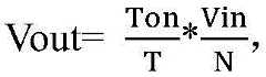 N is the primary and secondary side turn ratio of a transformer in the forward power circuit, Ton is the conduction duration of the forward power circuit controlled by the forward constant-current control device, and T is an on-off period of the forward power circuit. As mentioned above, the forward constant current control device provided by the present application uses the period of the PWM pulse signal as the on-off period for controlling the forward power circuit, and when the forward constant current control device normally works, the forward constant current control device controls the on-time of the forward power circuit based on the constant voltage control signal or the constant current control signal to realize the output of the constant voltage or the output of the constant current, and at this stage, it controls the duty ratio of the forward power circuit not to exceed the duty ratio of the PWM pulse signal. In this way, even if the input signal Vin acquired by the forward constant current control device is large, the load can still work within an acceptable power supply range.

However, when the forward constant current control device is abnormal in that the on-time of the forward power circuit cannot be controlled (that is, the constant voltage control signal or the constant current control signal is not present all the time during the high level period of the PWM pulse signal), for example, the received signal (for example, the feedback signal corresponding to the failure of the optocoupler) is abnormal due to the damage or failure of an external electronic component of the forward constant current control device (for example, the optocoupler coupled between the forward power circuit and the forward constant current control device for obtaining power supply of the load), or the constant voltage control unit or the constant current control unit is abnormal in that the constant voltage control unit or the constant current control unit cannot output or outputs the abnormal constant voltage control signal or the abnormal constant current control signal. The forward constant-current control device cannot change the conduction duration (i.e. duty ratio) of the forward power circuit, and can only control the forward power circuit to work according to the inherent duty ratio of the PWM pulse signal. However, since the inherent duty ratio of the PWM pulse signal is generally set to be larger, in the case that the obtained input signal Vin is also higher, the load power supply Vout may be higher than the maximum value acceptable by the load, thereby damaging the load.
In view of this, in another embodiment, the forward constant current control device further includes a Duty ratio adjusting unit on the basis of the circuit architecture shown in fig. 4 or fig. 7, for example, the Duty ratio adjusting unit is further included on the circuit architecture shown in fig. 7, please refer to fig. 15, which is shown as a circuit block diagram in another embodiment of the present application, the Dutyratio adjusting unit 25 has an input end P _252 and an output end P _251, the input end P _252 is used for connecting an external resistor R2 to sample an input signal Vin to obtain a sampling signal Vduty (for distinguishing from the aforementioned sampling signal Cs reflecting the peak current, the herein mentioned sampling signal Vduty is subsequently referred to as a first sampling signal), the output end P _251 is coupled to the drivingunit 23, and is used for outputting a Duty ratio adjusting signal Duty to the drivingunit 23 to control the forward power circuit to turn off when the on-time duration of the forward power circuit exceeds the time duration threshold, so that the load supply of the forward power circuit does not exceed the maximum protection threshold Vmax (which corresponds to the maximum supply acceptable to the load). In other words, the duration threshold determines the maximum value that the on-duration of the forward power circuit can reach, i.e., determines the maximum value of the duty cycle. It should be noted that fig. 15 is only an example, and on the basis of the circuit architecture shown in fig. 4, the connection manner and the operation principle of the dutyratio adjusting unit 25 are the same as those in fig. 15, and are not shown here.
The duration threshold is determined based on the first sampling signal Vduty, that is, when the forward power circuit receives different input signals Vin or the dutyratio adjusting unit 25 configures external resistors R2 with different impedances, the duration threshold is not the same fixed value, so that the forward constant current control device has strong applicability.
In an example, the dutycycle adjusting unit 25 adjusts the duration threshold based on the variation of the input signal Vin to maintain the stability of the maximum protection threshold Vmax. In particular, since the maximum protection threshold Vmax of the forward power circuit follows the aforementioned formula Wherein Tonmax is a time length threshold, and it can be known that the maximum protection threshold Vmax of the forward power circuit is not only related to the time length threshold of the forward constant current control device for controlling the forward power circuit, but also related to the input signal Vin. The input signal Vin is changed, and the duty
ratio adjusting unit 25 adjusts the duration threshold (i.e., adjusts the maximum value of the duty ratio) based on the change of the input signal Vin, so that the maximum protection threshold Vmax can be kept unchanged. Therefore, under the condition that the maximum value of the fixed duty ratio is set, the condition that the input signal Vin is enlarged to cause too-late protection, namely the load power supply exceeds the maximum value which can be born by the load, the forward constant current control device does not trigger protection, and the condition that the input signal Vin is reduced to cause too-early protection, namely the load power supply does not reach the maximum value which can be born by the load, is avoided, and the forward constant current control device controls the forward power circuit to not work. Therefore, for the same load, even if a user accesses the forward power circuit to different input signals Vin or the input signals Vin are unstable, the forward constant-current control device can also ensure that the maximum protection threshold value Vmax is unchanged, and the load can still be effectively protected.

In another example, the input signal Vin received by the forward power circuit is not changed, and the dutycycle adjusting unit 25 adjusts the duration threshold by configuring the external resistor R2 with different impedances to adapt to the input signal VinAt different maximum protection thresholds Vmax. In particular, see also the formulae Under the condition that the input signal Vin is not changed, if the time length threshold is not changed, the maximum protection threshold value Vmax is not changed, so that a user can only apply the forward constant current control device to a load with the bearing capacity above the maximum protection threshold value Vmax, and the protection is invalid for a load with the bearing capacity below the maximum protection threshold value Vmax, and the adaptability is poor. In this example, the user can configure the external resistor R2 with appropriate impedance for different loads, so that the forward constant current control device has high compatibility and can be applied to loads with various requirements.

Referring to fig. 16, which is a circuit block diagram of an embodiment of the duty ratio adjusting unit of the present application, the dutyratio adjusting unit 25 includes asecond delay circuit 251 and a current convertingcircuit 252. The input of the current convertingcircuit 252 is used as the input terminal P _252 of the dutyratio adjusting unit 25 to obtain the first sampling signal Vduty, and the output terminal P _253 of the current convertingcircuit 252 is coupled to the input of thesecond delay circuit 251 to convert the first sampling signal Vduty into an input current and output the input current to thesecond delay circuit 251. The output of thesecond delay circuit 251 is used as the output end P _251 of the Dutyratio adjusting unit 25, and is used for timing based on the input current to output the Duty ratio adjusting signal Duty when the on-time of the forward power circuit is judged to exceed the time threshold. Wherein the input current is associated with the duration threshold.
Referring to fig. 17, which is a schematic circuit diagram illustrating a current converting circuit according to an embodiment of the present invention, as shown in the figure, the current convertingcircuit 252 includes a resistor R3, a first pair of switching transistors (N4, N5), and a second pair of switching transistors (P5, P6). One end of the resistor R3 is coupled to the input terminal P _252 of the dutyratio adjusting unit 25, and the other end is coupled to the first end of the first pair of switching tubes (N4, N5). The second end of the first pair of switching tubes (N4, N5) is grounded Gnd, and the third end is coupled with the first end of the second pair of switching tubes (P5, P6). The second end of the second pair of switching tubes (P5, P6) is coupled to the power supply Vcc, and the third end is coupled to the output end P _253 of the current convertingcircuit 252. The resistor R3 converts the first sampling signal Vduty into a current signal, and the first pair of switching transistors (N4, N5) and the second pair of switching transistors (P5, P6) are coupled to form a current mirror circuit, so that the current signal outputs an input current Ib4 at an output terminal P _253 of thecurrent conversion circuit 252 to thesecond delay circuit 251. That is, the current value of the input current Ib4 has the same tendency of change as the first sampling signal Vduty, and the current value of the input current Ib4 increases as the first sampling signal Vduty becomes larger, and the current value of the input current Ib4 decreases as the first sampling signal Vduty becomes smaller. In practical application, the input current Ib4 is output to the timing capacitor in thesecond delay circuit 251, so that the timing capacitor is charged with the input current Ib4, and when the first sampling signal Vduty changes, the threshold duration is changed by changing the charging speed of the timing capacitor, so that the purpose of adjusting the maximum value of the duty ratio is achieved, so that the forward constant current control device has strong applicability and can maintain the maximum protection threshold to be stable.
Referring to fig. 18, a circuit structure of the second delay circuit of the present application in an embodiment is shown, and as shown in the figure, thesecond delay circuit 251 includes a secondtiming capacitor circuit 2511 and asecond switch circuit 2512. Thesecond timing capacitor 2511 has an input terminal P _254 and an output terminal P _255, and thesecond timing capacitor 2511 includes an inverter Ng2, switching transistors N6 and P7, and a timing capacitor C2. The input of the not gate Ng2 is used as the input terminal P _254 of the secondtiming capacitor circuit 2511, the control terminals of the switch tubes N6 and P7 are coupled to the output of the not gate Ng2 after being connected, the first terminal of the switch tube P7 is coupled to the output terminal P _253 of the current convertingcircuit 252, the second terminal of the switch tube N6 is grounded Gnd, the second terminal of the switch tube P7 and the first terminal of the switch tube N6 are connected to one terminal of the timing capacitor C2, one terminal of the timing capacitor C2 is further connected to the output terminal P _255, and the other terminal of the timing capacitor C2 is grounded Gnd. Thesecond switch circuit 2512 comprises a switch P8 and a not gate Ng3, wherein a control terminal of the switch P2 is connected to the output terminal P _255, a first terminal of the switch is coupled to the power supply Vcc, a second terminal of the switch is connected to the ground Gnd via the current source Ib5, the second terminal of the switch is further coupled to one terminal of the not gate Ng3, and the other terminal of the not gate Ng3 is connected to the output terminal P _251 of the dutyratio adjusting unit 25 to serve as the output of the dutyratio adjusting unit 25.
The input end P _254 of the secondtiming capacitor circuit 2511 is configured to be coupled to the driving unit to receive a logic signal Log output by the driving unit, so that the timing capacitor C2 performs timing operation based on the logic signal Log, where the logic signal Log can reflect the on and off durations of the forward power circuit, and the working principle of the driving unit outputting the logic signal Log is described in detail later, and is not expanded here. When the voltage signal of one electrode side of the timing capacitor C2 reaches the threshold voltage, thesecond switch circuit 2512 indicates that the on-time of the forward power circuit reaches the maximum protection threshold Vmax, so as to output the Duty ratio adjustment signal Duty through the output terminal P _ 251.
It should be noted that the circuit structure of thesecond delay circuit 251 shown in fig. 18 is only an example, and in other embodiments, the types and connection modes of the switching tubes in the secondtiming capacitor circuit 2511 shown in fig. 18 can be flexibly selected according to actual situations and matched with additional electronic components according to requirements, the principle of which is similar to that shown in fig. 18, and the intended function of thesecond delay circuit 251 in the present application is not affected. The switch P8 in thesecond switch circuit 2512 in fig. 18 may also be replaced by other types or other devices and flexibly select logic devices to be collocated according to the replaced devices to achieve the above functions, for example, thesecond switch circuit 2512 may include a comparator, one input terminal of the comparator is coupled to one end of the timing capacitor C1, the other input terminal of the comparator is used to obtain a reference voltage (may be a voltage signal generated by the power supply Vcc, and the magnitude of the voltage signal may be, for example, equal to the threshold voltage of the switch P8, and may be specifically set according to practice), and the comparator outputs the Duty ratio adjustment signal Duty when it is determined by comparison that one end of the timing capacitor C1 reaches the reference voltage obtained by the comparator. The second delay circuit of the present application is not limited to the circuit structure shown in fig. 18, and it is within the scope covered by the second delay circuit of the present application as long as the timing of the on or off duration of the forward power circuit to output the Duty ratio adjustment signal Duty can be completed based on the charging and discharging of the timing capacitor.
The following description illustrates the operation principle of the duty ratio adjusting circuit in one embodiment to implement the load protection function, as shown in fig. 16 to 18. Taking the example that the switch transistor N6 is an N-type MOSFET and the switch transistors P7 and P8 are P-type MOSFETs in fig. 18, in one on-off period T of the forward power circuit, thecurrent conversion circuit 252 obtains the first sampling signal Vduty and converts it into the input current Ib 4. In the turn-off stage of the forward power circuit, the logic signal Log is at a low level, and changes to a high level after passing through the nor gate Ng2 in thesecond delay circuit 251, the switching tube P7 is turned off, the switching tube N6 is turned on, and the charging capacitor C2 discharges through the switching tube N6. In the conducting stage of the forward power circuit, the logic signal Log is at a high level and changes to a low level after passing through the nor gate Ng2, the switching tube P7 is turned on, the switching tube N6 is turned off, and the input current Ib4 converted by thecurrent conversion circuit 252 flows into the switching tube P7 to charge the charging capacitor C2. If the voltage signal of one end of the charging capacitor C2, which is connected with the output end P _255, is at the threshold voltage corresponding to the turn-off point of the switching tube P8, it indicates that the on-time reaches the threshold time, the power supplied by the load reaches the maximum protection threshold Vmax, so that the switching tube P8 is in the off state, and the low level output by the second end of the switching tube P8 enables the nor gate Ng3 to output the high level as the Duty ratio adjustment signal Duty, so that the driving unit turns off the forward power circuit based on the signal. If the voltage signal of the end of the charging capacitor C2 connected to the output end P _255 does not exceed the threshold voltage corresponding to the turn-off point of the switch P8, the switch P8 is maintained at the on state, and the second end of the switch P8 is maintained at the high level, so that the not gate Ng3 outputs the low level. It should be noted that the current value of the input current Ib4 determines the charging speed of the charging capacitor C2, so that the threshold duration varies based on the variation of the input current Ib4, and the input current Ib4 is associated with the first sampling signal Vduty obtained by thecurrent conversion circuit 252, so that when the first sampling signal Vduty varies, the input current Ib4 varies, and the threshold duration also varies. For the variation relationship between the threshold duration and the first sampling signal Vduty and how to make the forward constant current control device achieve the functions of strong adaptability and maintaining the maximum protection threshold stable, please refer to the description of fig. 15 to 17, which is not described herein again.
As shown in fig. 4, 7 and 15, the constant voltage control signal Cv output by the constantvoltage control unit 21, the constant current control signal Cc output by the constantcurrent control unit 22, the short circuit protection signal Pro output by the shortcircuit protection unit 24 and the Duty ratio adjustment signal Duty output by the Dutyratio adjustment unit 25 are all output to the drivingunit 23, and the drivingunit 23 outputs a logic signal Log based on at least one of the signals to control the forward power circuit to be turned on or off for energy conversion based on the logic signal Log, so as to implement the above functions.
Please refer to fig. 19, which is a schematic waveform diagram of the driving unit outputting the logic signal based on each signal according to the present application, wherein the PWM is a PWM pulse signal generated inside the driving unit, and the logic signal Log output by the driving unit has a fixed period T, that is, the timing of the logic signal Log changing to the high level is determined by the PWM pulse signal. Based on the high level of the logic signal Log, the driving unit controls the forward power circuit to be in a conducting state. The duration of time that the high level of the logic signal Log can be maintained, that is, when the logic signal Log jumps from the high level to the low level, is determined by at least one of the constant voltage control signal Cv, the constant current control signal Cc, the short-circuit protection signal Pro, and the Duty ratio adjustment signal Duty. Based on the low level of the logic signal Log, the driving unit controls the forward power circuit to be in a turn-off state. When normally operating during a period in which the load current I is smaller than the preset constant current value Io, the constantvoltage control unit 21 outputs a constant voltage control signal Cv, and the driving unit determines a timing at which the logic signal Log becomes a low level based on the constant voltage control signal Cv. When the load current I is greater than the preset constant current value Io and the constantcurrent control unit 22 normally operates, the constantcurrent control unit 22 outputs a constant current control signal Cc, and the driving unit determines the timing when the logic signal Log becomes a low level based on the constant current control signal Cc, and during this period, once the load power supply is lower than the short-circuit protection threshold Vpro (i.e., the load voltage is low and the current is large), the short-circuit protection signal Pro output by the short-circuit protection unit 24 determines the timing when the logic signal Log becomes a low level based on the short-circuit protection signal Pro. During the output of the constant voltage or the output of the constant current, once the load supply greater than the maximum protection threshold Vmax (i.e., the maximum value that the load can withstand) occurs, the Duty ratio adjustment signal Duty is output by the Dutyratio adjustment unit 25, and the drive unit determines the timing at which the logic signal Log becomes the low level based on the Duty ratio adjustment signal Duty. It should be noted that, the Duty ratio adjustment signal Duty appearing during the period when the load current is smaller than the preset constant current value in fig. 19 is only an example, and is not a limitation on the timing when the Duty ratio adjustment signal Duty can appear, and actually, if the load power supply is larger than the maximum protection threshold Vmax during the period when the load current is larger than the preset constant current value, the Duty ratio adjustment signal Duty may also appear during the period when the load current is larger than the preset constant current value. In addition, when the short-circuit protection signal Pro or the Duty ratio adjustment signal Duty occurs, it is described that the forward constant current control device operates in an abnormal state, and the logic signal output by the driving unit continues to be at a low level for a preset time period (for example, 100T) or continues to be at a low level all the time.
Referring to fig. 20, which is a circuit block diagram of a driving unit according to an embodiment of the present invention, as shown, the drivingunit 23 includes aPWM generating circuit 231, alogic circuit 232, and adriving circuit 233. The output terminal of thePWM generating circuit 231 is coupled to thelogic circuit 232 to output the PWM pulse signal to thelogic circuit 232, thelogic circuit 232 is coupled to the output terminal P _213 of the constantvoltage control unit 21, the output terminal P _222 of the constantcurrent control unit 22, the output terminal P _243 of the short-circuit protection unit 24, and the output terminal P _251 of the Dutyratio adjusting unit 25, so that based on at least one of the constant voltage control signal Cv, the constant current control signal Cc, the short-circuit protection signal Pro, and the Duty ratio adjusting signal Duty, and the PWM pulse signal output logic signal Log, the drivingcircuit 233 is connected to the output of thelogic circuit 232 to control the forward power circuit to be turned on or off based on the logic signal Log to achieve the above-mentioned functions, and the specific implementation manner and the relationship among the signals are described with reference to the waveform illustration in fig. 19, and will not be described in detail herein. Thelogic circuit 232 includes, but is not limited to, a flip-flop, a timer, a selector, an and gate, a nor, etc. according to the control logic, which is not limited in this application.
In summary, the forward constant current control device provided by the application can control the forward power circuit to be switched from the output constant voltage to the output constant current when the load current exceeds the preset constant current value, and can be suitable for a high-power load with a constant current power supply requirement.
The application also discloses a control chip, the control chip is packaged with the forward constant current control device of any one of the above embodiments. In an embodiment, the chip is packaged with the constant current control unit, the constant voltage control unit, and the driving unit, where the pins include a first pin for acquiring a sampling signal reflecting a peak current of the forward power circuit, a second pin for acquiring a feedback signal reflecting a load current, a third pin for outputting a driving signal, a fourth pin for acquiring a power supply of the chip, and a fifth pin for grounding. In another embodiment, the chip is packaged with the constant current control unit, the constant voltage control unit, the short-circuit protection unit, and the driving unit as described above, and the plurality of pins include a first pin for acquiring a sampling signal reflecting a peak current of the forward power circuit, a second pin for acquiring a feedback signal reflecting a load current, a third pin for acquiring an input signal of the forward power circuit, a fourth pin for acquiring a power supply of the chip, and a fifth pin for grounding. In yet another embodiment, the chip package has the constant current control unit, the constant voltage control unit, the short-circuit protection unit, the duty ratio adjustment unit, and the driving unit as described above, and the plurality of pins includes a first pin for acquiring a first sampling signal obtained by sampling the rectified input signal, a second pin for acquiring a sampling signal reflecting a peak current of the forward power circuit, a third pin for acquiring a feedback signal, a fourth pin for outputting the driving signal, a fifth pin for acquiring the rectified input signal, a sixth pin for acquiring a power supply of the chip, and a seventh pin for grounding. The modules and circuits in the embodiments refer to the foregoing descriptions with reference to fig. 4 to fig. 20, which are not repeated herein.
Referring to fig. 21, a circuit block diagram of the forward constant current switching power supply in an embodiment of the present invention is shown, and as shown in the figure, the forward constant currentswitching power supply 30 includes a rectifyingcircuit 31, afilter circuit 32, a forward constantcurrent control device 33, aswitching device 34, and aforward power circuit 35.
The rectifyingcircuit 31 is configured to receive an external driving signal to output a rectified signal. The external driving signal may be, for example, an ac signal output by a utility grid, or may be a dc signal. Therectifier circuit 31 may be a full-wave rectifier circuit or a half-wave rectifier circuit including electronic components such as diodes for rectifying the received external drive signal and outputting a rectified signal.
Thefilter circuit 32 is coupled to therectifier circuit 31, and is configured to filter the rectified signal output by therectifier circuit 31 to output a filtered signal to theforward power circuit 35. In an embodiment, thefilter circuit 32 may be a pi filter circuit, an LC filter circuit, an RC filter circuit, an LC pi filter circuit, an RC pi filter circuit, or the like, which is not limited in this application.
The forward constantcurrent control device 33 is configured to output a driving signal, and the forward constantcurrent control device 33 may adopt the forward constant current control device disclosed in the present application, and the structure and the working principle thereof please refer to the description of fig. 4 to fig. 20, which is not described herein again.
A control terminal of theswitching device 34 is coupled to the forward constantcurrent control device 33, and is configured to be turned on or off based on the driving signal. In an embodiment, the switching device is a three-terminal controllable device that can be controlled to be turned on and off by a control signal, and the three-terminal controllable device includes a control terminal, a first terminal, and a second terminal, and the control terminal controls the turn-on or turn-off between the first terminal and the second terminal based on a received driving signal. The three-terminal controllable device includes a controllable Transistor, such as a Metal-oxide-semiconductor Field-effect Transistor (MOSFET) or a Bipolar Junction Transistor (BJT).
Theforward power circuit 35 is coupled between thefilter circuit 32 and theswitching device 34, and configured to perform energy conversion on a received input signal based on turning on or off of theswitching device 34 so as to switch from an output constant voltage to an output constant current when a load current reaches a preset constant current value; wherein the input signal is the filtered signal. It should be noted that, in some embodiments, thefilter circuit 32 may not be included, in which case theforward power circuit 35 is coupled between the rectifyingcircuit 31 and theswitching device 34, and the input signal received by theforward power circuit 35 is a rectified signal.
The application also discloses a forward constant current control method, which is applied to a forward constant current control device adopting pulse width modulation. The forward constant current control method includes steps S20, S21, S22, and S23 (not shown).
In step S20, the forward constant current control device acquires a feedback signal and a sampling signal.
Referring to the descriptions of fig. 4, fig. 7, and fig. 15, the forward constant current control device includes a constant voltage control unit, a constant current control unit, and a driving unit. The constant voltage control device acquires a feedback signal and a sampling signal, the constant current control unit acquires the sampling signal, the feedback signal reflects the load current of a forward power circuit controlled by the forward constant current control device, and the sampling signal reflects the peak current of the forward power circuit.
In step S21, the constant voltage control unit outputs a constant voltage control signal based on the feedback signal and the sampling signal during a period in which the load current is less than a preset constant current value, under the control of the constant voltage control signal, the forward power circuit outputs constant voltage power supply to a load.
In some embodiments, the constant voltage control unit compares the sampling signal and the feedback signal to output the constant voltage control signal during a period in which the feedback signal is less than a first reference signal, wherein the first reference signal reflects a preset constant current value. Specifically, please refer to the description of fig. 4 and 5 for the circuit structure and the operation principle of the constant voltage control unit, which are not described herein again.
In step S22, when the load current reaches the preset constant current value, a constant current control signal is output based on the sampling signal, and the forward power circuit outputs a constant current to the load for supplying power under the control of the constant current control signal.
In some embodiments, the constant current control unit compares the sampling signal with a first reference signal to output the constant current control signal during a period in which the feedback signal is smaller than the first reference signal, wherein the first reference signal reflects a preset constant current value. Specifically, please refer to the description of fig. 4 and fig. 6 for the circuit structure and the operation principle of the constant current control unit, which are not described herein again.
In the stage that the forward power circuit outputs the constant current, the load current is stabilized at the preset constant current value, so that the load voltage can change along with the change of the load resistance, and if the load voltage is too low and the load resistance is too small, the load can still be maintained at the preset constant current value and exceed the maximum value which can be borne by the load, thereby damaging the load.
In view of this, please refer to the description of fig. 7, the forward constant current control apparatus further includes a short-circuit protection unit, and the short-circuit protection unit outputs a short-circuit protection signal to control the forward power circuit to implement short-circuit protection in the constant current stage when the load voltage is lower than the short-circuit protection threshold. Please refer to the description of fig. 7 to fig. 14 for the circuit structure and the operation principle of the short-circuit protection unit, which are not described herein again.
In step S23, the driving unit drives the forward power circuit to switch from outputting a constant voltage to outputting a constant current when the load current reaches a preset constant current value based on the constant voltage control signal or the constant current control signal.
As can be seen from the descriptions of fig. 4, 7, and 15, the driving unit is connected to the constant voltage control unit, the constant current control unit, the short-circuit protection unit, and the duty ratio adjustment unit, so that the driving unit outputs a logic signal based on at least one of the signals output by the units to control the forward power circuit to be turned on or off based on the logic signal so as to switch the output constant voltage to the output constant current when the load current reaches a preset constant current value, and can implement protection when the load power supply exceeds the maximum load bearable value during the constant voltage period and implement short-circuit protection during the constant current period. For the circuit structure and the operation principle of the driving unit, please refer to the description of fig. 19 and fig. 20, which is not repeated herein.
As can be seen from steps S20 to S23, the forward constant current control device provided in the present application uses the period of the PWM pulse signal output by the pulse width modulation as the on-off period for controlling the forward power circuit, and when the forward constant current control device normally operates, the forward constant current control device controls the on-time of the forward power circuit based on the constant voltage control signal or the constant current control signal to output the constant voltage or output the constant current, and at this stage, it controls the duty ratio of the forward power circuit not to exceed the duty ratio of the PWM pulse signal. In this way, even in the case that the input signal acquired by the forward constant current control device is large, the load can be enabled to work within an acceptable power supply range.
However, when the forward constant current control device is abnormal in that the on-time of the forward power circuit cannot be controlled (that is, the constant voltage control signal or the constant current control signal is not present all the time during the high level period of the PWM pulse signal), for example, the received signal (for example, the feedback signal corresponding to the failure of the optocoupler) is abnormal due to the damage or failure of an external electronic component of the forward constant current control device (for example, the optocoupler coupled between the forward power circuit and the forward constant current control device for obtaining power supply of the load), or the constant voltage control unit or the constant current control unit is abnormal in that the constant voltage control unit or the constant current control unit cannot output or outputs the abnormal constant voltage control signal or the abnormal constant current control signal. The forward constant-current control device cannot change the conduction duration (i.e. duty ratio) of the forward power circuit, and can only control the forward power circuit to work according to the inherent duty ratio of the PWM pulse signal. However, since the inherent duty cycle of the PWM pulse signal is generally set to be large, in the case that the acquired input signal is also high, the power supplied to the load may be higher than the maximum value acceptable by the load, and the load may be damaged.
In view of this, the forward constant current control method further includes step S24 (not shown), in step S24, the forward constant current control device outputs a duty ratio adjustment signal to control the forward power circuit to turn off when determining that the on duration of the forward power circuit exceeds the preset duration threshold (i.e., when the power supplied by the load exceeds the maximum protection threshold).
In an embodiment, please refer to the description of fig. 15, the forward constant current control device further includes a duty ratio adjusting unit, and the forward constant current control device outputs a duty ratio adjusting signal to control the forward power circuit to turn off when the on-time of the forward power circuit is determined to exceed the preset time threshold (that is, when the power supplied by the load exceeds the maximum protection threshold) by the duty ratio adjusting unit. Please refer to the description of fig. 15 to fig. 18 for the circuit structure and the operation principle of the duty ratio adjusting unit, which are not described herein again.
In summary, the forward constant current control device, the system, the control method and the chip provided by the application can control the forward power circuit to switch from the output constant voltage to the output constant current when the load current exceeds the preset constant current value, and can be suitable for a high-power load with a constant current power supply requirement.
The above embodiments are merely illustrative of the principles and utilities of the present application and are not intended to limit the application. Any person skilled in the art can modify or change the above-described embodiments without departing from the spirit and scope of the present application. Accordingly, it is intended that all equivalent modifications or changes which can be made by those skilled in the art without departing from the spirit and technical concepts disclosed in the present application shall be covered by the claims of the present application.
Claims (17)
1. A forward constant current control device, which is used for controlling a forward power circuit to perform energy conversion, comprises:
the constant voltage control unit is used for outputting a constant voltage control signal based on the acquired feedback signal and the sampling signal when the load current is smaller than a preset constant current value; wherein the feedback signal reflects a load current of the forward power circuit, and the sampling signal reflects a peak current of the forward power circuit;
the constant current control unit is used for outputting a constant current control signal based on the sampling signal when the load current reaches the preset constant current value;
and the driving unit is coupled with the constant voltage control unit and the constant current control unit and used for driving the forward power circuit to output constant voltage power supply to a load or output constant current power supply to the load based on the constant voltage control signal or the constant current control signal.
2. The forward constant-current control device according to claim 1, wherein the constant-current control unit includes a first comparison circuit for comparing the sampling signal with a first reference signal to output the constant-current control signal; wherein the first reference signal reflects the preset constant current value.
3. The forward constant-current control device according to claim 2, wherein the constant-voltage control unit includes a second comparison circuit for comparing the sampling signal and the feedback signal to output the constant-voltage control signal during a period in which the feedback signal is smaller than the first reference signal.
4. The forward constant current control device according to claim 1, further comprising a short-circuit protection unit, coupled to the driving unit, for outputting a short-circuit protection signal to the driving unit during a period when the load voltage is lower than a short-circuit protection threshold value to control the forward power circuit to implement short-circuit protection during a period when the constant current power is output to the load.
5. The forward constant current control device of claim 4, wherein the short-circuit protection unit is further configured to maintain the short-circuit protection threshold stable based on the obtained rectified input signal.
6. The forward constant current control device according to claim 4, wherein the short-circuit protection unit includes:
the first time delay circuit is coupled with the constant current control unit and used for forbidding the constant current control unit when the conducting duration of the forward power circuit is lower than the reference duration; wherein the reference duration is associated with the short-circuit protection threshold;
and the third comparison circuit is coupled to the driving unit and used for comparing the sampling signal with the second reference signal to output a comparison signal serving as the short-circuit protection signal to the driving unit.
7. The forward constant-current control device according to claim 6, wherein the first delay circuit includes:
the first timing capacitor circuit comprises a timing capacitor and is used for executing timing operation;
the first switch circuit is coupled to the first timing capacitor circuit and is used for disabling the constant current control unit when a voltage signal on one electrode side of the timing capacitor reaches a threshold voltage of the switch circuit.
8. The forward constant current control device as claimed in claim 6, wherein the short-circuit protection unit further comprises a compensation circuit, coupled to the first delay circuit, for compensating the reference time duration based on the obtained variation of the rectified input signal to maintain the stability of the short-circuit protection threshold.
9. The forward constant current control device as claimed in claim 8, wherein the compensation circuit changes the reference duration by changing a charging speed of a timing capacitor.
10. The forward constant current control device according to claim 6, wherein the short-circuit protection unit further comprises: and the timing circuit is coupled with the third comparison circuit and the driving unit and used for timing based on the comparison signal and outputting the short-circuit protection signal to the driving unit to control the forward constant current control device to stop working after timing is finished.
11. The forward constant current control device according to claim 1, further comprising: and the duty ratio adjusting unit is coupled with the driving unit and used for outputting a duty ratio adjusting signal to the driving unit to control the forward power circuit to be switched off when the on duration of the forward power circuit exceeds a duration threshold.
12. The forward constant current control device according to any one of claims 1 to 11, wherein the drive unit includes:
a PWM generating circuit for generating a PWM pulse signal;
a logic circuit, coupled to the PWM generation circuit and at least one of the constant voltage control unit, the constant current control unit, the short-circuit protection unit, and the duty ratio adjustment unit, for outputting a logic signal based on at least one of the PWM pulse, the constant voltage control signal, the constant current control signal, the short-circuit protection signal, and the duty ratio adjustment signal;
and the driving circuit is coupled to the logic circuit and used for outputting a driving signal based on the logic signal to control the forward power circuit to be switched on or switched off so as to perform energy conversion.
13. A control chip, wherein the chip is packaged with the forward constant current control device as claimed in any one of claims 1 to 12.
14. A forward constant current switching power supply, comprising:
a rectifying circuit for receiving an external driving signal to output a rectified signal;
the filter circuit is coupled to the rectifying circuit and used for filtering the rectifying signal to output a filtered signal;
a forward constant current control device as claimed in any one of claims 1 to 12 for outputting a drive signal;
the control end of the switching device is coupled with the forward constant current control device and used for switching on or off based on the driving signal;
the forward power circuit is coupled with the switching device and used for performing energy conversion on the received input signal based on the on or off of the switching device so as to switch the output constant voltage into the output constant current when the load current reaches a preset constant current value; wherein the input signal is the filtered signal.
15. A forward constant current control method is characterized by being used for controlling a forward power circuit to convert energy and comprising the following steps:
acquiring a feedback signal and a sampling signal;
outputting a constant voltage control signal based on the feedback signal and the sampling signal during a period when the load current is less than a preset constant current value; wherein the feedback signal reflects a load current of the forward power circuit, and the sampling signal reflects a peak current of the forward power circuit;
outputting a constant current control signal based on the sampling signal when the load current reaches the preset constant current value;
and driving the forward power circuit to output constant voltage power supply to a load or output constant current power supply to the load based on the constant voltage control signal or the constant current control signal.
16. The forward constant current control method according to claim 15, further comprising the steps of: and outputting a short-circuit protection signal to control the forward power circuit to realize short-circuit protection in a constant current stage when the load voltage is lower than a short-circuit protection threshold value.
17. The forward constant current control method according to claim 15, further comprising the steps of: and when the on-time of the forward power circuit exceeds a preset time threshold, outputting a duty ratio adjusting signal to control the forward power circuit to be switched off.
Priority Applications (1)
| Application Number | Priority Date | Filing Date | Title |
|---|---|---|---|
| CN202010786038.1ACN114070105B (en) | 2020-08-05 | 2020-08-05 | Forward constant current control device, switching power supply, control method and chip |
Applications Claiming Priority (1)
| Application Number | Priority Date | Filing Date | Title |
|---|---|---|---|
| CN202010786038.1ACN114070105B (en) | 2020-08-05 | 2020-08-05 | Forward constant current control device, switching power supply, control method and chip |
Publications (2)
| Publication Number | Publication Date |
|---|---|
| CN114070105Atrue CN114070105A (en) | 2022-02-18 |
| CN114070105B CN114070105B (en) | 2025-08-22 |
Family
ID=80232627
Family Applications (1)
| Application Number | Title | Priority Date | Filing Date |
|---|---|---|---|
| CN202010786038.1AActiveCN114070105B (en) | 2020-08-05 | 2020-08-05 | Forward constant current control device, switching power supply, control method and chip |
Country Status (1)
| Country | Link |
|---|---|
| CN (1) | CN114070105B (en) |
Cited By (5)
| Publication number | Priority date | Publication date | Assignee | Title |
|---|---|---|---|---|
| CN114421781A (en)* | 2022-03-31 | 2022-04-29 | 深圳市芯茂微电子有限公司 | Control method of resonant converter |
| CN114756075A (en)* | 2022-03-31 | 2022-07-15 | 上海新进芯微电子有限公司 | Peak current load control circuit |
| WO2023184845A1 (en)* | 2022-03-31 | 2023-10-05 | 上海新进芯微电子有限公司 | Peak current load control circuit |
| CN120150523A (en)* | 2025-05-16 | 2025-06-13 | 深圳麦格米特电气股份有限公司 | High voltage constant current device and printing equipment |
| CN120150523B (en)* | 2025-05-16 | 2025-10-17 | 深圳麦格米特电气股份有限公司 | High voltage constant current device and printing equipment |
Citations (5)
| Publication number | Priority date | Publication date | Assignee | Title |
|---|---|---|---|---|
| JPH10225116A (en)* | 1997-02-07 | 1998-08-21 | Sanken Electric Co Ltd | Dc power supply device |
| JP2015225825A (en)* | 2014-05-30 | 2015-12-14 | 日立アプライアンス株式会社 | Led lamp, led lighting device and led illumination system |
| CN105491713A (en)* | 2015-12-23 | 2016-04-13 | 浙江闲兴光电科技有限公司 | High-power LED street lamp drive circuit |
| CN107276432A (en)* | 2016-04-08 | 2017-10-20 | 上海芯熠微电子有限公司 | Switching mode AC-DC converter and its control circuit |
| CN108093661A (en)* | 2016-02-05 | 2018-05-29 | 广东欧珀移动通信有限公司 | Adapter and charge control method |
- 2020
- 2020-08-05CNCN202010786038.1Apatent/CN114070105B/enactiveActive
Patent Citations (5)
| Publication number | Priority date | Publication date | Assignee | Title |
|---|---|---|---|---|
| JPH10225116A (en)* | 1997-02-07 | 1998-08-21 | Sanken Electric Co Ltd | Dc power supply device |
| JP2015225825A (en)* | 2014-05-30 | 2015-12-14 | 日立アプライアンス株式会社 | Led lamp, led lighting device and led illumination system |
| CN105491713A (en)* | 2015-12-23 | 2016-04-13 | 浙江闲兴光电科技有限公司 | High-power LED street lamp drive circuit |
| CN108093661A (en)* | 2016-02-05 | 2018-05-29 | 广东欧珀移动通信有限公司 | Adapter and charge control method |
| CN107276432A (en)* | 2016-04-08 | 2017-10-20 | 上海芯熠微电子有限公司 | Switching mode AC-DC converter and its control circuit |
Cited By (5)
| Publication number | Priority date | Publication date | Assignee | Title |
|---|---|---|---|---|
| CN114421781A (en)* | 2022-03-31 | 2022-04-29 | 深圳市芯茂微电子有限公司 | Control method of resonant converter |
| CN114756075A (en)* | 2022-03-31 | 2022-07-15 | 上海新进芯微电子有限公司 | Peak current load control circuit |
| WO2023184845A1 (en)* | 2022-03-31 | 2023-10-05 | 上海新进芯微电子有限公司 | Peak current load control circuit |
| CN120150523A (en)* | 2025-05-16 | 2025-06-13 | 深圳麦格米特电气股份有限公司 | High voltage constant current device and printing equipment |
| CN120150523B (en)* | 2025-05-16 | 2025-10-17 | 深圳麦格米特电气股份有限公司 | High voltage constant current device and printing equipment |
Also Published As
| Publication number | Publication date |
|---|---|
| CN114070105B (en) | 2025-08-22 |
Similar Documents
| Publication | Publication Date | Title |
|---|---|---|
| US9812975B2 (en) | Resonant converter with capacitive mode control and associated control method | |
| US9621068B2 (en) | Load driving circuit and method thereof | |
| US9263939B2 (en) | Capacitor discharging circuit and converter | |
| US8310845B2 (en) | Power supply circuit with a control terminal for different functional modes of operation | |
| TWI441404B (en) | Capacitor discharging circuit and power converter using same | |
| CN103066853B (en) | Control circuit, switching power supply and control method thereof | |
| US8587968B2 (en) | Control circuits and methods for switching mode power supplies | |
| CN105515355B (en) | System and method for dc-dc converter | |
| US8634212B2 (en) | Controller and controlling method for power converter | |
| TWI589106B (en) | Switching power supplies and switch controllers | |
| US9431895B2 (en) | High power-factor control circuit and power supply | |
| US20150280578A1 (en) | Isolated power converter and switching power supply using the same | |
| WO2016028942A1 (en) | Driving circuit, lighting device and method of reducing power dissipation | |
| US9078319B2 (en) | Conversion control circuit and converter thereof | |
| CN114070105B (en) | Forward constant current control device, switching power supply, control method and chip | |
| US11606037B2 (en) | Detection circuit and switching converter | |
| US11350503B2 (en) | Power converter | |
| JP2006340538A (en) | Switching power supply | |
| CN111432523A (en) | BUCK constant current control circuit with input voltage changing along with output voltage and power supply | |
| TW202147058A (en) | Pfc controller with multi-function node, related pfc circuit and control method | |
| CN112653324B (en) | Boost converter system without direct power supply | |
| CN104124862B (en) | High PFC constant-current control devices and voltage changer without loop compensation | |
| CN114172391B (en) | Constant power reference modulation circuit, control device and chip, power supply device and method | |
| JP2015216763A (en) | Switching power supply circuit | |
| CN114070104B (en) | Forward switching power supply, forward system control device, control method and chip |
Legal Events
| Date | Code | Title | Description |
|---|---|---|---|
| PB01 | Publication | ||
| PB01 | Publication | ||
| SE01 | Entry into force of request for substantive examination | ||
| SE01 | Entry into force of request for substantive examination | ||
| GR01 | Patent grant | ||
| GR01 | Patent grant |