CN114003198B - Inner product processing unit, arbitrary precision calculation device, method, and readable storage medium - Google Patents
Inner product processing unit, arbitrary precision calculation device, method, and readable storage mediumDownload PDFInfo
- Publication number
- CN114003198B CN114003198BCN202111221317.4ACN202111221317ACN114003198BCN 114003198 BCN114003198 BCN 114003198BCN 202111221317 ACN202111221317 ACN 202111221317ACN 114003198 BCN114003198 BCN 114003198B
- Authority
- CN
- China
- Prior art keywords
- vector
- unit
- bit
- data
- vectors
- Prior art date
- Legal status (The legal status is an assumption and is not a legal conclusion. Google has not performed a legal analysis and makes no representation as to the accuracy of the status listed.)
- Active
Links
Images


Classifications
- G—PHYSICS
- G06—COMPUTING OR CALCULATING; COUNTING
- G06F—ELECTRIC DIGITAL DATA PROCESSING
- G06F7/00—Methods or arrangements for processing data by operating upon the order or content of the data handled
- G06F7/38—Methods or arrangements for performing computations using exclusively denominational number representation, e.g. using binary, ternary, decimal representation
- G06F7/48—Methods or arrangements for performing computations using exclusively denominational number representation, e.g. using binary, ternary, decimal representation using non-contact-making devices, e.g. tube, solid state device; using unspecified devices
- G06F7/57—Arithmetic logic units [ALU], i.e. arrangements or devices for performing two or more of the operations covered by groups G06F7/483 – G06F7/556 or for performing logical operations
- G—PHYSICS
- G06—COMPUTING OR CALCULATING; COUNTING
- G06F—ELECTRIC DIGITAL DATA PROCESSING
- G06F15/00—Digital computers in general; Data processing equipment in general
- G06F15/76—Architectures of general purpose stored program computers
- G06F15/78—Architectures of general purpose stored program computers comprising a single central processing unit
- G06F15/7807—System on chip, i.e. computer system on a single chip; System in package, i.e. computer system on one or more chips in a single package
- G06F15/7821—Tightly coupled to memory, e.g. computational memory, smart memory, processor in memory
- G—PHYSICS
- G06—COMPUTING OR CALCULATING; COUNTING
- G06F—ELECTRIC DIGITAL DATA PROCESSING
- G06F17/00—Digital computing or data processing equipment or methods, specially adapted for specific functions
- G06F17/10—Complex mathematical operations
- G06F17/16—Matrix or vector computation, e.g. matrix-matrix or matrix-vector multiplication, matrix factorization
- G—PHYSICS
- G06—COMPUTING OR CALCULATING; COUNTING
- G06F—ELECTRIC DIGITAL DATA PROCESSING
- G06F7/00—Methods or arrangements for processing data by operating upon the order or content of the data handled
- G06F7/38—Methods or arrangements for performing computations using exclusively denominational number representation, e.g. using binary, ternary, decimal representation
- G06F7/48—Methods or arrangements for performing computations using exclusively denominational number representation, e.g. using binary, ternary, decimal representation using non-contact-making devices, e.g. tube, solid state device; using unspecified devices
- G06F7/544—Methods or arrangements for performing computations using exclusively denominational number representation, e.g. using binary, ternary, decimal representation using non-contact-making devices, e.g. tube, solid state device; using unspecified devices for evaluating functions by calculation
- G06F7/5443—Sum of products
- Y—GENERAL TAGGING OF NEW TECHNOLOGICAL DEVELOPMENTS; GENERAL TAGGING OF CROSS-SECTIONAL TECHNOLOGIES SPANNING OVER SEVERAL SECTIONS OF THE IPC; TECHNICAL SUBJECTS COVERED BY FORMER USPC CROSS-REFERENCE ART COLLECTIONS [XRACs] AND DIGESTS
- Y02—TECHNOLOGIES OR APPLICATIONS FOR MITIGATION OR ADAPTATION AGAINST CLIMATE CHANGE
- Y02A—TECHNOLOGIES FOR ADAPTATION TO CLIMATE CHANGE
- Y02A90/00—Technologies having an indirect contribution to adaptation to climate change
- Y02A90/10—Information and communication technologies [ICT] supporting adaptation to climate change, e.g. for weather forecasting or climate simulation
Landscapes
- Engineering & Computer Science (AREA)
- Physics & Mathematics (AREA)
- Theoretical Computer Science (AREA)
- General Physics & Mathematics (AREA)
- Computing Systems (AREA)
- General Engineering & Computer Science (AREA)
- Pure & Applied Mathematics (AREA)
- Mathematical Optimization (AREA)
- Mathematical Analysis (AREA)
- Computational Mathematics (AREA)
- Mathematical Physics (AREA)
- Computer Hardware Design (AREA)
- Data Mining & Analysis (AREA)
- Algebra (AREA)
- Databases & Information Systems (AREA)
- Software Systems (AREA)
- Microelectronics & Electronic Packaging (AREA)
- Complex Calculations (AREA)
Abstract
Description
Translated fromChinese技术领域Technical Field
本发明一般地涉及计算机领域。更具体地,本发明涉及内积处理部件、任意精度计算设备、方法及可读存储介质。The present invention generally relates to the field of computers, and more particularly to an inner product processing unit, an arbitrary precision computing device, a method, and a readable storage medium.
背景技术Background Art
任意精确计算是利用任意位数来表示操作数,在许多技术领域至关重要,例如超新星模拟、气候模拟、原子模拟、人工智能、行星轨道计算等。这些领域需要处理数百、甚至数千或数百万位数的数据,这样大范围的数据位数处理远远超出了传统处理器的硬件能力。Arbitrary precision computing is the use of arbitrary number of bits to represent operands, which is crucial in many technical fields, such as supernova simulation, climate simulation, atomic simulation, artificial intelligence, planetary orbit calculation, etc. These fields need to process hundreds, even thousands or millions of digits of data, and such a large range of data bit processing is far beyond the hardware capabilities of traditional processors.
即使现有技术使用高位宽的处理器,也无法处理任意精确计算操作所需的可变长度,原因在于:最优比特宽在不同算法之间变化很大,且比特宽的细微差异会导致显著的成本差异。再者,现有技术还提出了许多提高体系结构级计算效率的技术,主要是纯效计算(effectual-only computation)和近似计算,前者只执行基本计算,其中无效的计算像是稀疏化和重复数据会被跳过或消除,后者使用较不准确的数据像是低位宽数据或量化后数据,来代替原始的准确数据的计算。然而,对于纯效计算来说,要找到重复数据十分困难且昂贵,对于近似计算来说,它直观地与任意精确计算的目的相矛盾,任意精确计算需要精确的计算来获得较高的精度。最后,这些现有技术不可避免地都会导致大量低效的内存访问。Even if the prior art uses a high-bitwidth processor, it cannot handle the variable length required for arbitrary precision computing operations because the optimal bitwidth varies greatly between different algorithms, and slight differences in bitwidth can lead to significant cost differences. Furthermore, the prior art has also proposed many techniques to improve the efficiency of architectural-level computing, mainly effectual-only computation and approximate computation, the former only performs basic computations, in which invalid computations such as sparsification and duplicate data are skipped or eliminated, and the latter uses less accurate data such as low-bitwidth data or quantized data to replace the original accurate data calculation. However, for effectual-only computation, it is very difficult and expensive to find duplicate data, and for approximate computation, it intuitively contradicts the purpose of arbitrary precision computation, which requires accurate computation to obtain higher precision. Finally, these prior art techniques inevitably lead to a large number of inefficient memory accesses.
因此,一种高效的任意精确计算方案是迫切需要的。Therefore, an efficient arbitrary precision computation scheme is urgently needed.
发明内容Summary of the invention
为了至少部分地解决背景技术中提到的技术问题,本发明的方案提供了一种内积处理部件、任意精度计算设备、方法及可读存储介质。In order to at least partially solve the technical problems mentioned in the background technology, the solution of the present invention provides an inner product processing component, an arbitrary precision computing device, a method and a readable storage medium.
在一个方面中,本发明揭露一种用以内积第一向量与第二向量的处理部件,包括:转换单元、多个内积单元及合成单元。转换单元用以根据第一向量的长度及位宽生成多个模式向量。每个内积单元基于第二向量在长度方向上的数据向量为索引,累加多个模式向量中的特定模式向量,以形成单位累加数列。合成单元用以加总多个单位累加数列,以获得内积结果。In one aspect, the present invention discloses a processing unit for inner product of a first vector and a second vector, comprising: a conversion unit, a plurality of inner product units and a synthesis unit. The conversion unit is used to generate a plurality of pattern vectors according to the length and bit width of the first vector. Each inner product unit is based on the data vector of the second vector in the length direction as an index, and accumulates a specific pattern vector in the plurality of pattern vectors to form a unit accumulation sequence. The synthesis unit is used to sum up the plurality of unit accumulation sequences to obtain the inner product result.
在另一个方面,本发明揭露一种任意精度计算加速器,连接至片外内存,任意精度计算加速器包括:核内存代理器、核控制器及处理阵列。核内存代理器用以自片外内存读取多个操作数。核控制器用以将多个操作数拆分成多个向量,多个向量包括第一向量及第二向量。处理阵列包括多个处理部件,处理部件用以根据第一向量及第二向量的长度,内积第一向量与第二向量,以获得内积结果。其中,核控制器将内积结果整合成多个操作数的计算结果,核内存代理器将计算结果存储至片外内存。In another aspect, the present invention discloses an arbitrary precision computing accelerator connected to an off-chip memory, the arbitrary precision computing accelerator comprising: a core memory agent, a core controller and a processing array. The core memory agent is used to read multiple operands from the off-chip memory. The core controller is used to split the multiple operands into multiple vectors, the multiple vectors including a first vector and a second vector. The processing array comprises multiple processing components, the processing components are used to perform an inner product of the first vector and the second vector according to the lengths of the first vector and the second vector to obtain an inner product result. The core controller integrates the inner product result into a calculation result of the multiple operands, and the core memory agent stores the calculation result to the off-chip memory.
在另一个方面,本发明揭露一种集成电路装置,包括前述的任意精度计算加速器、处理装置及片外内存。处理装置用以控制任意精度计算加速器,片外内存包括LLC。其中,任意精度计算加速器与处理装置通过LLC联系。In another aspect, the present invention discloses an integrated circuit device, comprising the aforementioned arbitrary precision computing accelerator, a processing device and an off-chip memory. The processing device is used to control the arbitrary precision computing accelerator, and the off-chip memory includes LLC. The arbitrary precision computing accelerator is connected to the processing device via LLC.
在另一个方面,本发明揭露一种板卡,包括前述的集成电路装置。In another aspect, the present invention discloses a board comprising the aforementioned integrated circuit device.
在另一个方面,本发明揭露一种内积第一向量与第二向量的方法,包括:根据第一向量的长度及位宽生成多个模式向量;基于第二向量在长度方向上的数据向量为索引,累加多个模式向量中的特定模式向量,以形成多个单位累加数列;以及加总多个单位累加数列,以获得内积结果。In another aspect, the present invention discloses a method for inner product of a first vector and a second vector, comprising: generating multiple pattern vectors according to the length and bit width of the first vector; accumulating specific pattern vectors in the multiple pattern vectors based on the data vector of the second vector in the length direction as an index to form multiple unit accumulation series; and summing up the multiple unit accumulation series to obtain the inner product result.
在另一个方面,本发明揭露一种任意精度计算方法,包括:自片外内存读取多个操作数;将多个操作数拆分成多个向量,多个向量包括第一向量及第二向量;根据第一向量及第二向量的长度,内积第一向量与第二向量,以获得内积结果;将内积结果整合成多个操作数的计算结果;以及将计算结果存储至片外内存。In another aspect, the present invention discloses an arbitrary precision calculation method, comprising: reading multiple operands from an off-chip memory; splitting the multiple operands into multiple vectors, the multiple vectors including a first vector and a second vector; inner producting the first vector and the second vector according to the lengths of the first vector and the second vector to obtain an inner product result; integrating the inner product result into a calculation result of the multiple operands; and storing the calculation result to the off-chip memory.
在另一个方面,本发明揭露一种计算机可读存储介质,其上存储有任意精度计算的计算机程序代码,当所述计算机程序代码由处理装置运行时,执行前述的方法。In another aspect, the present invention discloses a computer-readable storage medium having a computer program code for arbitrary precision calculation stored thereon. When the computer program code is executed by a processing device, the aforementioned method is executed.
本发明提出一种处理任意精度计算方案,并行处理不同的比特流,其部署了完整的比特串行数据路径,以灵活弹性地执行高精度计算。本发明充分利用简易硬件配置,减少重复计算,进而实现低能耗的任意精确计算。The present invention proposes a solution for processing arbitrary precision calculations, processing different bit streams in parallel, and deploying a complete bit serial data path to flexibly perform high-precision calculations. The present invention makes full use of simple hardware configurations, reduces repeated calculations, and thus achieves arbitrary precision calculations with low energy consumption.
附图说明BRIEF DESCRIPTION OF THE DRAWINGS
通过参考附图阅读下文的详细描述,本发明示例性实施方式的上述以及其他目的、特征和优点将变得易于理解。在附图中,以示例性而非限制性的方式示出了本发明的若干实施方式,并且相同或对应的标号表示相同或对应的部分。其中:The above and other objects, features and advantages of the exemplary embodiments of the present invention will become readily understood by reading the detailed description below with reference to the accompanying drawings. In the accompanying drawings, several embodiments of the present invention are shown in an exemplary and non-limiting manner, and the same or corresponding reference numerals represent the same or corresponding parts. Among them:
图1是示出本发明实施例的板卡的结构图;FIG1 is a block diagram showing a board according to an embodiment of the present invention;
图2是示出本发明实施例的集成电路装置的结构图;2 is a block diagram showing an integrated circuit device according to an embodiment of the present invention;
图3是示出本发明实施例的计算装置的内部结构示意图;3 is a schematic diagram showing the internal structure of a computing device according to an embodiment of the present invention;
图4是示出示例性乘法运算的示意图;FIG4 is a schematic diagram illustrating an exemplary multiplication operation;
图5是示出本发明实施例的转换单元的示意图;FIG5 is a schematic diagram showing a conversion unit according to an embodiment of the present invention;
图6是示出本发明实施例的生成单元的示意图;FIG6 is a schematic diagram showing a generating unit according to an embodiment of the present invention;
图7是示出本发明实施例的内积单元的示意图;FIG7 is a schematic diagram showing an inner product unit according to an embodiment of the present invention;
图8是示出本发明实施例的合成单元的示意图;FIG8 is a schematic diagram showing a synthesis unit according to an embodiment of the present invention;
图9是示出本发明实施例的全加器组的示意图;9 is a schematic diagram showing a full adder group according to an embodiment of the present invention;
图10是示出本发明另一实施例的任意精度计算的流程图;以及FIG10 is a flowchart showing arbitrary precision calculation according to another embodiment of the present invention; and
图11是示出本发明另一实施例的内积第一向量与第二向量的流程图。FIG. 11 is a flow chart showing the inner product of a first vector and a second vector according to another embodiment of the present invention.
具体实施方式DETAILED DESCRIPTION
下面将结合本发明实施例中的附图,对本发明实施例中的技术方案进行清楚、完整地描述,显然,所描述的实施例是本发明一部分实施例,而不是全部的实施例。基于本发明中的实施例,本领域技术人员在没有做出创造性劳动前提下所获得的所有其他实施例,都属于本发明保护的范围。The following will be combined with the drawings in the embodiments of the present invention to clearly and completely describe the technical solutions in the embodiments of the present invention. Obviously, the described embodiments are part of the embodiments of the present invention, not all of the embodiments. Based on the embodiments of the present invention, all other embodiments obtained by those skilled in the art without creative work are within the scope of protection of the present invention.
应当理解,本发明的权利要求、说明书及附图中的术语“第一”、“第二”、“第三”和“第四”等是用于区别不同对象,而不是用于描述特定顺序。本发明的说明书和权利要求书中使用的术语“包括”和“包含”指示所描述特征、整体、步骤、操作、元素和/或组件的存在,但并不排除一个或多个其它特征、整体、步骤、操作、元素、组件和/或其集合的存在或添加。It should be understood that the terms "first", "second", "third" and "fourth" etc. in the claims, specifications and drawings of the present invention are used to distinguish different objects rather than to describe a specific order. The terms "include" and "comprise" used in the specification and claims of the present invention indicate the presence of the described features, wholes, steps, operations, elements and/or components, but do not exclude the presence or addition of one or more other features, wholes, steps, operations, elements, components and/or their collections.
还应当理解,在此本发明说明书中所使用的术语仅仅是出于描述特定实施例的目的,而并不意在限定本发明。如在本发明说明书和权利要求书中所使用的那样,除非上下文清楚地指明其它情况,否则单数形式的“一”、“一个”及“该”意在包括复数形式。还应当进一步理解,在本发明说明书和权利要求书中使用的术语“和/或”是指相关联列出的项中的一个或多个的任何组合以及所有可能组合,并且包括这些组合。It should also be understood that the terms used in this specification of the present invention are only for the purpose of describing specific embodiments and are not intended to limit the present invention. As used in the specification of the present invention and the claims, the singular forms of "a", "an" and "the" are intended to include the plural forms unless the context clearly indicates otherwise. It should also be further understood that the term "and/or" used in the specification of the present invention and the claims refers to any combination of one or more of the associated listed items and all possible combinations, and includes these combinations.
如在本说明书和权利要求书中所使用的那样,术语“如果”可以依据上下文被解释为“当...时”或“一旦”或“响应于确定”或“响应于检测到”。As used in this specification and claims, the term "if" may be interpreted as "when" or "upon" or "in response to determining" or "in response to detecting," depending on the context.
下面结合附图来详细描述本发明的具体实施方式。The specific embodiments of the present invention are described in detail below with reference to the accompanying drawings.
任意精度计算在许多科技领域中都起到关键作用。举例来说,看似平凡的方程式x3+y3+z3=3,利用计算机求解会需要200位以上的精度;在伊辛理论(Ising theory)中,计算积分需要1000位以上的精度;而计算双曲空间(hyperbolic space)中的结点余空间(knot complement)的体积则涉及高达60000位精度。一个非常微小的精度误差都可能导致计算结果的巨大差异,因此任意精度计算在计算机领域是十分严肃的技术课题。Arbitrary precision computing plays a key role in many scientific and technological fields. For example, the seemingly ordinary equation x3 +y3 +z3 = 3 requires more than 200 digits of precision to solve using a computer; in Ising theory, calculating integrals requires more than 1,000 digits of precision; and calculating the volume of the knot complement in hyperbolic space involves up to 60,000 digits of precision. A very small precision error can lead to a huge difference in the calculation results, so arbitrary precision computing is a very serious technical issue in the computer field.
本发明提出了一种高效的任意精度计算加速器架构,其主要参考内积运算的计算形式,突出加速器架构的操作内并行性(intra-parallelism)和操作间并行性(inter-parallelism),以实现操作数的乘法运算。The present invention proposes an efficient arbitrary precision computing accelerator architecture, which mainly refers to the calculation form of inner product operation, highlights the intra-parallelism and inter-parallelism of the accelerator architecture, so as to realize the multiplication operation of operands.
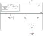
图1示出本发明实施例的一种板卡10的结构示意图。如图1所示,板卡10包括芯片101,其是一种系统级芯片(System on Chip,SoC),或称片上系统,集成有一个或多个组合处理装置,组合处理装置是一种人工智能运算单元,用以支持各类深度学习和机器学习算法,满足计算机视觉、语音、自然语言处理、数据挖掘等领域复杂场景下的智能处理需求。特别是深度学习技术大量应用在云端智能领域,云端智能应用的一个显著特点是输入数据量大,对平台的存储能力和计算能力有很高的要求,此实施例的板卡10适用在云端智能应用,具有庞大的片外存储、片上存储和强大的计算能力。FIG1 shows a schematic diagram of the structure of a
芯片101通过对外接口装置102与外部设备103相连接。外部设备103例如是服务器、计算机、摄像头、显示器、鼠标、键盘、网卡或wifi接口等。待处理的数据可以由外部设备103通过对外接口装置102传递至芯片101。芯片101的计算结果可以经由对外接口装置102传送回外部设备103。根据不同的应用场景,对外接口装置102可以具有不同的接口形式,例如PCIe接口等。The
板卡10还包括用于存储数据的存储器件104,其包括一个或多个存储单元105。存储器件104通过总线与控制器件106和芯片101进行连接和数据传输。板卡10中的控制器件106配置用于对芯片101的状态进行调控。为此,在一个应用场景中,控制器件106可以包括单片机(Micro Controller Unit,MCU)。The
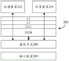
图2是示出此实施例的芯片101中的组合处理装置的结构图。如图2中所示,组合处理装置包括计算装置201、处理装置202、片外内存203、通信节点204及接口装置205。在此实施例中,有几种集成方案可以用来协同计算装置201、处理装置202、片外内存203的工作,其中图2A示出LLC集成方案,图2B示出SoC集成方案,图2C示出IO集成方案。Fig. 2 is a block diagram showing a combined processing device in the
计算装置201配置成执行用户指定的操作,主要实现为多核智能处理器,用以执行深度学习或机器学习的计算,其可以与处理装置202进行交互,以共同完成用户指定的操作。计算装置201内含前述的任意精度计算加速器,用以处理线性计算,更详细来说是应用在如卷积中的操作数乘法运算。The computing device 201 is configured to perform user-specified operations, and is mainly implemented as a multi-core intelligent processor to perform deep learning or machine learning calculations, which can interact with the processing device 202 to jointly complete the user-specified operations. The computing device 201 contains the aforementioned arbitrary precision computing accelerator to process linear calculations, more specifically, operand multiplication operations such as convolution.
处理装置202作为通用的处理器,执行包括但不限于数据搬运、对计算装置201的开启和/或停止、非线性计算等基本控制。根据实现方式的不同,处理装置202可以是中央处理器(central processing unit,CPU)、图形处理器(graphics processing unit,GPU)或其他通用和/或专用处理器中的一种或多种类型的处理器,这些处理器包括但不限于数字信号处理器(digital signal processor,DSP)、专用集成电路(application specificintegrated circuit,ASIC)、现场可编程门阵列(field-programmable gate array,FPGA)或者其他可编程逻辑器件、分立门或者晶体管逻辑器件、分立硬件组件等,并且其数目可以根据实际需要来确定。当将计算装置201和处理装置202整合共同考虑时,二者视为形成异构多核结构。The processing device 202 is a general-purpose processor that performs basic controls including but not limited to data handling, starting and/or stopping the computing device 201, nonlinear calculations, etc. Depending on the implementation, the processing device 202 can be a central processing unit (CPU), a graphics processing unit (GPU), or one or more types of processors in other general and/or special processors, including but not limited to digital signal processors (DSP), application specific integrated circuits (ASIC), field-programmable gate arrays (FPGA) or other programmable logic devices, discrete gates or transistor logic devices, discrete hardware components, etc., and their number can be determined according to actual needs. When the computing device 201 and the processing device 202 are integrated and considered together, the two are considered to form a heterogeneous multi-core structure.
片外内存203用以存储待处理与处理完的数据,其层次根据延迟时间从小到大,可以划分为:一级缓存(L1)、二级缓存(L2)、三级缓存(L3,又称为LLC)与实体内存。实体内存为DDR,大小通常为16G或更大。当计算装置201或处理装置202欲从片外内存203读取数据时,由于L1的速度最快,故通常会优先访问L1,如果数据未存放在L1,接着访问L2,如果数据亦未存放在L2,继续访问L3,如果数据仍未存放在L3,最后访问DDR。片外内存203的缓存层次结构是通过将最常访问的数据存储在缓存中来加快数据访问速度。与缓存相比,DDR相当慢。随着缓存级别的增加(L1→L2→LLC→DDR),访问延迟越来越高,但存储空间越来越大。The off-
通信节点204是片上网络(network-on-chip,NoC)中的路由节点或路由器,当计算装置201或处理装置202产生一个数据包后,会通过特定的接口发送到通信节点204中,通信节点204读取数据包的头微片中的地址信息,利用特定的路由算法计算出最佳路由路径,从而建立可靠的传输路径将数据包送到目的节点(例如片外内存203)。同样地,当计算装置201或处理装置202需从片外内存203读取数据包时,通信节点204亦会计算出最佳路由路径,将数据包从片外内存203发送到计算装置201或处理装置202。The communication node 204 is a routing node or router in the network-on-chip (NoC). When the computing device 201 or the processing device 202 generates a data packet, it will be sent to the communication node 204 through a specific interface. The communication node 204 reads the address information in the header microchip of the data packet and calculates the best routing path using a specific routing algorithm, thereby establishing a reliable transmission path to send the data packet to the destination node (such as the off-chip memory 203). Similarly, when the computing device 201 or the processing device 202 needs to read a data packet from the off-
接口装置205是组合处理装置对外的输入输出接口,当组合处理装置与外部设备交换信息时,由于外部设备种类繁多,每种设备对传输的信息的要求各不相同,接口装置205会根据数据传输的发送方与接收方的要求,执行设置数据缓冲以解决两者速度差异所带来的不协调问题、设置信号电平转换、设置信息转换逻辑以满足对各自格式的要求、设置时序控制电路来同步发送方与接收方的工作及提供地址转码等任务。The interface device 205 is the external input and output interface of the combined processing device. When the combined processing device exchanges information with external devices, due to the wide variety of external devices, each device has different requirements for the transmitted information. The interface device 205 will perform tasks such as setting data buffers to solve the incoordination problem caused by the speed difference between the two, setting signal level conversion, setting information conversion logic to meet the requirements of each format, setting timing control circuits to synchronize the work of the sender and the receiver, and providing address transcoding according to the requirements of the sender and the receiver of the data transmission.
图2A的LLC集成指的是计算装置201与处理装置202通过LLC联系,图2B的SoC集成是通过通信节点204来集成计算装置201、处理装置202与片外内存203。图2C的IO集成是通过接口装置205来集成计算装置201、处理装置202与片外内存203。这3种集成方式仅为示例,本发明并不限制集成的方式。The LLC integration in FIG2A refers to the connection between the computing device 201 and the processing device 202 via LLC, and the SoC integration in FIG2B refers to the integration of the computing device 201, the processing device 202, and the off-
此实施例较佳地选择LLC集成方案。由于深度学习和机器学习的核心是卷积算子,卷积算子的基础是内积运算,内积运算又是由乘法与加法组合而成,因此,计算装置201的主要任务是大量的乘法和加法等低级运算,在执行神经网络模型的训练与推理时,计算装置201与处理装置202需要密集的交互,将计算装置201与处理装置202集成到LLC中,通过LLC共享数据,以达到较低的交互成本。再者,由于高精度数据可能具有数百万位,L1与L2的容量有限,通过L1与L2交互会导致容量不足的问题。计算装置201利用LLC的相对大容量来缓存高精度数据,以节省重复访问的时间。This embodiment preferably selects the LLC integration solution. Since the core of deep learning and machine learning is the convolution operator, the basis of the convolution operator is the inner product operation, and the inner product operation is composed of a combination of multiplication and addition, the main task of the computing device 201 is a large number of low-level operations such as multiplication and addition. When performing training and reasoning of the neural network model, the computing device 201 and the processing device 202 need to interact intensively. The computing device 201 and the processing device 202 are integrated into the LLC, and data is shared through the LLC to achieve a lower interaction cost. Furthermore, since high-precision data may have millions of bits, the capacity of L1 and L2 is limited, and interaction through L1 and L2 will cause insufficient capacity. The computing device 201 uses the relatively large capacity of the LLC to cache high-precision data to save time for repeated access.
图3示出计算装置201的内部结构示意图,其包括核内存代理器301、核控制器302及处理阵列303。FIG3 is a schematic diagram showing the internal structure of the computing device 201 , which includes a
核内存代理器301作为计算装置201访问片外内存203的管理端。当核内存代理器301自片外内存203读取操作数时,操作数的起始地址在核内存代理器301中被设置,核内存代理器301通过自增加地址来同时、连续、串行读取多个操作数,其读取方式是一次性地自这些操作数的低位逐次往高位读取,例如需要读取3个操作数时,先根据各操作数的起始地址串行读取第一操作数的最低位512比特,再串行读取第二操作数的低位512比特,接着串行读取第三操作数的低位512比特,最低位读取完成后,通过自增加地址(增加512比特),接着串行读取各次低位512比特,依此方式直到这3个操作数的最高位被读取。当核内存代理器301将计算结果存储回片外内存203时,则以并行发送,例如核内存代理器301需要发送3个计算结果至片外内存203,则同时发送这3个计算结果的最低位比特,再同时发送这3个计算结果的次低位比特,依此方式直到这3个计算结果的最高位比特同时发送完毕。一般来说,这些操作数是以矩阵或向量的形式来表示的。The
核控制器302基于处理阵列303中的处理部件的运算能力与数量,控制将每个操作数拆分成多个数据段,也就是多个向量,使得核内存代理器301以数据段为单位发送至处理阵列303。The
处理阵列303用以执行两个操作数的乘法计算,举例来说,第一操作数可以拆分成x0至x7等8个数据段,第二操作数可以拆分成y0至y3等4个数据段,当第一操作数与第二操作数执行乘法运算时,算法展开如图4所示。处理阵列303便是通过拆分第一操作数与第二操作数,分别进行内积计算,再将中间结果401、402、403及404移位对齐加总,以获得乘法运算的计算结果。The
为清楚地阐述技术方案,以下统一将上述数据段视为向量来表示,两数据段相乘即是两向量(第一向量及第二向量)做内积,其中第一向量来自第一操作数,第二向量来自第二操作数。To clearly explain the technical solution, the above data segments are uniformly regarded as vectors below. The multiplication of two data segments is the inner product of two vectors (the first vector and the second vector), where the first vector comes from the first operand and the second vector comes from the second operand.
处理阵列303包括多个处理部件304,这些处理部件304以阵列方式排列,图中示例性展示4×8个处理部件304,本发明不限制处理部件304的个数。每个处理部件304用以根据第一向量的长度及第二向量的长度,内积第一向量与第二向量,以获得内积结果。最后,核控制器302控制内存代理器301将内积结果整合或归约成多个操作数的计算结果,发送给核内存代理器301,核内存代理器301将计算结果存储至片外内存203。The
具体来说,计算装置201在控制上采用递推分解算法(recursivedecomposition),当计算装置201接收到来自处理装置202的指令来执行任意精度计算时,核控制器302将乘法的操作数平均拆分为多个向量,并将它们发送到处理阵列303进行计算,每个处理部件304负责一组向量的计算,例如第一向量与第二向量的内积。在此实施例中,每个处理部件304会基于本身的硬件资源,将一组向量进一步拆分成更小的内积计算单元,以方便进行内积计算。计算装置201在数据路径上采用多比特流,即每个操作数以每周期1比特的速度从核内存代理器301导入处理部件303,但多个操作数同时并行传输,在计算结束后,处理部件304以比特串行方式发送内积结果到核内存代理器301。Specifically, the computing device 201 uses a recursive decomposition algorithm in control. When the computing device 201 receives an instruction from the processing device 202 to perform arbitrary precision calculations, the
作为计算装置201的核心计算单元,处理部件304的主要任务是内积计算。处理部件304是基于比特索引向量内积的流程分成3个阶段来处理,第一阶段为模式生成阶段,第二阶段为模式索引阶段,第三阶段为加权合成阶段。As the core computing unit of the computing device 201, the main task of the
以第一向量


此实施例将第二向量

其中K是一个固定不变且大小为N×2N二进制矩阵,Bcol是一个大小为2N×py的二进制矩阵,C是py加权向量。Where K is a fixed binary matrix of size N × 2N , Bcol is a binary matrix of
在第一向量


换言之,一旦第一向量

Bcol是一位有效向量(one-hot vector),每一列只有1个元素为1,其余元素为0,而哪个元素为1取决于第二向量


将第二向量


Bcol的第一列只有第四个元素为1,表示第二向量


C是py加权向量,用以反映第二向量


此实施例通过上述的方式来拆解第二向量


处理部件304便是用以基于前述的转换来实现向量内积


图3进一步示出处理部件304的结构示意图。为实现前述3个阶段,处理部件304包括处理部件内存代理单元305、处理部件控制单元306、转换单元307、多个内积单元308及合成单元309。3 further shows a schematic diagram of the structure of the
处理部件内存代理单元305作为处理部件304访问核内存代理器301的接口端,用以接收需要进行内积运算的两向量,例如前述的第一向量

处理部件控制单元306用以协调并管理处理部件304中各单元的工作。The processing
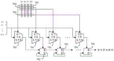
转换单元307用以实现模式生成阶段。自处理部件内存代理单元305接收第一向量


N个比特流输入端501用以对应至第一向量


生成组件502为执行


在第一向量
图6示出单位向量为(1011)的生成单元504的示意图。以生成单元504为例,其模拟的是单位向量(1011),故生成单元504包括3个元素暂存器601、加法器602及进位暂存器603。3个元素暂存器601接收并暂存数据向量对应至所模拟的单位向量的比特值,也就是x0、x1、x3的比特值,直接忽略x2的比特值,以此结构来实现:FIG6 shows a schematic diagram of a

暂存器601中的数值会被送至加法器602进行累加,累加后如果出现进位,则进位的数值被暂存在进位暂存器603,与下一周期输入的x0、x1、x3的比特值相加,直到第px周期将x0、x1、x3的最高位比特相加为止。每个生成单元都根据同样的技术逻辑进行设计,本领域技术人员基于图6中实现单位向量为(1011)的生成单元504的结构,无须创造性劳动便可轻易推及其他生成单元的结构,故不赘述。需特别注意的是,有些生成单元无需设置加法器602与进位暂存器603,例如模拟单元向量(0000)、(0001)、(0010)、(0100)及(1000)的生成单元,这些生成单元在同一周期中仅有一个输入,不存在加法运算更不会发生进位的情况。The value in the
回到图5,2N个比特流输出端503分别连接至每个生成单元的加法器602的输出,用以输出2N个模式向量


z0=0z0 = 0
z1=x0z1 = x0
z2=x1z2 = x1
z3=x0+x1z3 = x0 + x1
z4=x2z4 = x2
z5=x0+x2z5 = x0 + x2
z6=x1+x2z6 = x1 + x2
z7=x0+x1+x2z7 = x0 + x1 + x2
z8=x3z8 = x3
z9=x0+x3z9 = x0 + x3
z10=x1+x3z10 = x1 + x3
z11=x0+x1+x3z11 = x0 + x1 + x3
z12=x2+x3z12 = x2 + x3
z13=x0+x2+x3z13 = x0 + x2 + x3
z14=x1+x2+x3z14 = x1 + x2 + x3
z15=x0+x1+x2+x3z15 = x0 + x1 + x2 + x3
模式向量


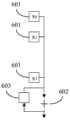
图7示出此实施例的内积单元308的示意图。为了实现
py个多路复用器701用以实现模式索引阶段。每个多路复用器701接收所有的模式向量


多路复用器701判断输入的同位数据向量与二进制矩阵K的哪个单位向量相同,输出相同单位向量所对应的特定模式向量。例如,最高位同位数据向量703作为选择信号输入至第一多路复用器,假设最高位同位数据向量703为(0101),与图5中的单位向量505相同,则第一多路复用器将输出与单位向量505相对应的特定模式向量z5。再例如,次高位同位数据向量704作为选择信号输入至第二多路复用器,假设次高位同位数据向量704为(0010),与图5中的单位向量506相同,则第二多路复用器将输出与单位向量506相对应的特定模式向量z2。最后,最低位同位数据向量705作为选择信号输入至第py多路复用器,假设最低位同位数据向量705为(1110),与图5中的单位向量507相同,则第py多路复用器将输出与单位向量507相对应的特定模式向量z14。至此完成
串行全加器702实现加权合成阶段。py-1个串行全加器702依图中方式串行连接,接收多路复用器701输出特定模式向量,依序累加这些特定模式向量,以获得单位累加数列。需特别注意的是,为符合从低位开始累加并进位(如有)至下一位使得下一位可以正确地累加并进位,最低位同位数据向量705所对应的特定模式向量必须安排输入至最外侧的串行全加器702,使得低位的同位数据向量所对应的特定模式向量优先被累加,越高位的同位数据向量所对应的特定模式向量则安排输入至越内侧的串行全加器702,最高位同位数据向量703所对应的特定模式向量必须安排输入至最内侧的串行全加器702,使得越高位的同位数据向量所对应的特定模式向量越滞后被累加,如此才能确保累加的正确性,也就是依照py加权向量C以反映第二向量

合成单元309用以执行如图4中的加总计算405。合成单元309接收来自各个内积单元308的单位累加数列,每个单位累加数列就如同图4中的中间结果401、402、403及404,这些中间结果在内积单元308中已对齐,接着合成单元309加总这些对齐后的单位累加数列,进而获得第一向量

图8示出此实施例的合成单元309的示意图。图中的合成单元309示例性地接收8个内积单元308的输出,即单位累加数列801至808。这些单位累加数列801至808是第一向量

图9示出全加器组810至815的示意图。全加器组810至815包括第一全加器901与第二全加器902,第一全加器901与第二全加器902分别包括多路复用器903及904,其中多路复用器903的输入端连接加法器的进位输出与数值0,多路复用器904的输入端连接加法器的进位输出与数值1,该数值0与1分别用以模拟前一位数的中间结果加总后未进位与进位,故第一全加器901用以生成前一位数未进位的中间结果总和,第二全加器902用以生成前一位数进位的中间结果总和。这样的结构可以不用等待前一位数的中间结果来决定是否进位,此实施例改采同步计算未进位与进位的设计能降低运算延迟时间。全加器组810至815还包括多路复用器905,两个中间结果总和均输入至多路复用器905,多路复用器905会根据前一位数的计算结果是否进位,来选择输出进位的中间结果总和或是未进位的中间结果总和。累加过后的输出818即为第一向量

回到图8,由于最低位的运算不可能产生进位,因此次低位的全加器组809仅包括第一全加器901,直接生成未进位的中间结果,无需设置第二全加器902及多路复用器905。Returning to FIG. 8 , since the operation of the lowest bit cannot generate a carry, the second lowest bit
根据图8、图9及其相关说明,当此实施例的合成单元309欲加总M个单位累加数列时,将配置M-1个全加器组,其中包括M-1个第一全加器901、M-2个第二全加器902及M-2个多路复用器905。According to Figures 8 and 9 and their related descriptions, when the
在其他情况下,合成单元309可以弹性选择开启或关闭全加器组的运作,例如第一向量

回到图3,在合成单元309获得第一向量

基于上述的结构,此实施例的计算装置201根据操作数的长度执行不同数量的内积运算。进一步地,处理阵列303可以控制索引在纵向的处理部件304间共享,并控制模式向量在横向的处理部件304间共享,以高效地进行运算。Based on the above structure, the computing device 201 of this embodiment performs different numbers of inner product operations according to the length of the operand. Further, the
在数据路径管理上,此实施例采用两级架构,即核内存代理器301和处理部件内存代理单元305。操作数在LLC中的起始地址记录于核内存代理器301中,核内存代理器301通过自增加地址来同时、连续、串行自LLC读取多个操作数。源地址是自增长的,因此数据块的顺序是确定的。核控制器302决定哪些处理部件304接收数据块,处理部件控制单元306再决定哪些内积单元308接收这些数据块。In terms of data path management, this embodiment adopts a two-level architecture, namely, the
本发明的另一个实施例是一种任意精度计算方法,可以利用前述实施例的硬件结构来实现。图10示出此实施例的流程图。Another embodiment of the present invention is an arbitrary precision calculation method, which can be implemented using the hardware structure of the above embodiment. FIG10 shows a flow chart of this embodiment.
在步骤1001中,自片外内存读取多个操作数。当自片外内存读取操作数时,操作数的起始地址在核内存代理器中被设置,核内存代理器通过自增加地址来同时、连续、串行读取多个操作数,其读取方式是一次性地自这些操作数的低位逐次往高位读取。In
在步骤1002中,将多个操作数拆分成多个向量,多个向量包括第一向量及第二向量。核控制器基于处理阵列中的处理部件的运算能力与数量,控制将每个操作数拆分成多个数据段,也就是多个向量,使得核内存代理器以数据段为单位发送至处理阵列。In
在步骤1003中,根据第一向量及第二向量的长度,内积第一向量与第二向量,以获得内积结果。处理阵列包括多个处理部件,这些处理部件以阵列方式排列,每个处理部件根据第一向量的长度及第二向量的长度,内积第一向量与第二向量,以获得内积结果。更详细来说,在此步骤中,先执行模式生成阶段,再执行模式索引阶段,最后执行加权合成阶段。In
以第一向量


其中K是一个固定不变且大小为N×2N二进制矩阵,Bcol是一个大小为2N×py的二进制矩阵,C是py加权向量,K、Bcol、C的定义与前述实施例无异,故不赘述。此实施例通过上述的方式来拆解第二向量


在模式生成阶段,此实施例获得


在步骤1101中,根据第一向量的长度及位宽生成多个模式向量。首先,对应至第一向量


在模拟单位向量时,先接收并暂存对应至该单位向量的数据向量的比特值,这些比特值会被累加,累加后如果出现进位,则进位的数值被暂存在进位暂存器,与下一周期输入的数据向量的比特值相加,直到第px周期将数据向量的最高位比特值相加为止。When simulating a unit vector, the bit value of the data vector corresponding to the unit vector is first received and temporarily stored. These bit values will be accumulated. If a carry occurs after the accumulation, the carry value will be temporarily stored in the carry register and added to the bit value of the data vector input in the next cycle until the highest bit value of the data vector is added in the px cycle.
最后,接收累加后的结果,即为模式向量


在步骤1102中,基于第二向量


更详细来说,,根据第二向量


接着,判断输入的同位数据向量与二进制矩阵K的哪个单位向量相同,输出相同单位向量所对应的特定模式向量。至此完成
最后,依序累加这些特定模式向量,以获得单位累加数列。需特别注意的是,应确保累加的正确性,也就是依照py加权向量C以反映第二向量

在步骤1103中,加总多个单位累加数列,以获得内积结果。为了实现同步计算,此实施例将第一向量

此实施例采同步计算未进位与进位的设计以降低运算延迟时间。未进位与进位的中间结果总和同时获得,再根据前一位数的计算结果是否进位,来选择输出进位的中间结果总和或是未进位的中间结果总和。累加过后的输出即为第一向量

回到图10,在步骤1004中,将内积结果整合成多个操作数的计算结果。核控制器控制内存代理器将内积结果整合或归约成多个操作数的计算结果,发送给核内存代理器。Returning to Fig. 10, in
在步骤1005中,将计算结果存储至片外内存。核内存代理器并行发送计算结果,先同时发送这些计算结果的最低位比特,再同时发送这些计算结果的次低位比特,依此方式直到这些计算结果的最高位比特同时发送完毕。In
本发明另一个实施例为一种计算机可读存储介质,其上存储有任意精度计算的计算机程序代码,当所述计算机程序代码由处理器运行时,执行如图10或图11的方法。在一些实现场景中,上述集成的单元可以采用软件程序模块的形式来实现。如果以软件程序模块的形式实现并作为独立的产品销售或使用时,所述集成的单元可以存储在计算机可读取存储器中。基于此,当本发明的方案以软件产品(例如计算机可读存储介质)的形式体现时,该软件产品可以存储在存储器中,其可以包括若干指令用以使得计算机设备(例如个人计算机、服务器或者网络设备等)执行本发明实施例所述方法的部分或全部步骤。前述的存储器可以包括但不限于U盘、闪存盘、只读存储器(Read Only Memory,ROM)、随机存取存储器(Random Access Memory,RAM)、移动硬盘、磁碟或者光盘等各种可以存储程序代码的介质。Another embodiment of the present invention is a computer-readable storage medium, on which a computer program code for arbitrary precision calculation is stored, and when the computer program code is run by a processor, a method as shown in Figure 10 or Figure 11 is executed. In some implementation scenarios, the above-mentioned integrated unit can be implemented in the form of a software program module. If it is implemented in the form of a software program module and sold or used as an independent product, the integrated unit can be stored in a computer-readable memory. Based on this, when the solution of the present invention is embodied in the form of a software product (such as a computer-readable storage medium), the software product can be stored in a memory, which may include several instructions to enable a computer device (such as a personal computer, a server or a network device, etc.) to perform some or all of the steps of the method described in the embodiment of the present invention. The aforementioned memory may include, but is not limited to, various media that can store program codes, such as a USB flash drive, a flash drive, a read-only memory (ROM), a random access memory (RAM), a mobile hard disk, a magnetic disk or an optical disk.
本发明提出一种新颖的架构,用以有效地处理任意精度计算。不论操作数的精度多高,本发明都可以将操作数进行拆解,利用索引并行处理固定长度的比特流,避免比特级冗余,像是稀疏性或重复计算等问题,无需配置高位宽的硬件,便可达到灵活运用和大位宽计算的效果。The present invention proposes a novel architecture for effectively processing arbitrary precision calculations. No matter how high the precision of the operands is, the present invention can disassemble the operands and use indexes to process fixed-length bit streams in parallel, avoiding bit-level redundancy, such as sparsity or repeated calculations, and can achieve the effect of flexible use and large-bit-width calculation without configuring high-bit-width hardware.
根据不同的应用场景,本发明的电子设备或装置可以包括服务器、云端服务器、服务器集群、数据处理装置、机器人、电脑、打印机、扫描仪、平板电脑、智能终端、PC设备、物联网终端、移动终端、手机、行车记录仪、导航仪、传感器、摄像头、相机、摄像机、投影仪、手表、耳机、移动存储、可穿戴设备、视觉终端、自动驾驶终端、交通工具、家用电器、和/或医疗设备。所述交通工具包括飞机、轮船和/或车辆;所述家用电器包括电视、空调、微波炉、冰箱、电饭煲、加湿器、洗衣机、电灯、燃气灶、油烟机;所述医疗设备包括核磁共振仪、B超仪和/或心电图仪。本发明的电子设备或装置还可以被应用于互联网、物联网、数据中心、能源、交通、公共管理、制造、教育、电网、电信、金融、零售、工地、医疗等领域。进一步,本发明的电子设备或装置还可以用于云端、边缘端、终端等与人工智能、大数据和/或云计算相关的应用场景中。在一个或多个实施例中,根据本发明方案的算力高的电子设备或装置可以应用于云端设备(例如云端服务器),而功耗小的电子设备或装置可以应用于终端设备和/或边缘端设备(例如智能手机或摄像头)。在一个或多个实施例中,云端设备的硬件信息和终端设备和/或边缘端设备的硬件信息相互兼容,从而可以根据终端设备和/或边缘端设备的硬件信息,从云端设备的硬件资源中匹配出合适的硬件资源来模拟终端设备和/或边缘端设备的硬件资源,以便完成端云一体或云边端一体的统一管理、调度和协同工作。According to different application scenarios, the electronic equipment or device of the present invention may include a server, a cloud server, a server cluster, a data processing device, a robot, a computer, a printer, a scanner, a tablet computer, a smart terminal, a PC device, an Internet of Things terminal, a mobile terminal, a mobile phone, a driving recorder, a navigator, a sensor, a camera, a camera, a video camera, a projector, a watch, a headset, a mobile storage, a wearable device, a visual terminal, an automatic driving terminal, a vehicle, a household appliance, and/or a medical device. The vehicle includes an airplane, a ship, and/or a vehicle; the household appliance includes a television, an air conditioner, a microwave oven, a refrigerator, an electric rice cooker, a humidifier, a washing machine, an electric light, a gas stove, and a range hood; the medical device includes a nuclear magnetic resonance apparatus, a B-ultrasound apparatus, and/or an electrocardiograph. The electronic equipment or device of the present invention can also be applied to the Internet, the Internet of Things, a data center, energy, transportation, public administration, manufacturing, education, power grid, telecommunications, finance, retail, construction sites, medical treatment and other fields. Further, the electronic equipment or device of the present invention can also be used in the cloud, edge end, terminal and other application scenarios related to artificial intelligence, big data and/or cloud computing. In one or more embodiments, electronic devices or apparatuses with high computing power according to the solutions of the present invention can be applied to cloud devices (such as cloud servers), while electronic devices or apparatuses with low power consumption can be applied to terminal devices and/or edge devices (such as smart phones or cameras). In one or more embodiments, the hardware information of the cloud device and the hardware information of the terminal device and/or edge device are compatible with each other, so that according to the hardware information of the terminal device and/or edge device, appropriate hardware resources can be matched from the hardware resources of the cloud device to simulate the hardware resources of the terminal device and/or edge device, so as to complete the unified management, scheduling and collaborative work of end-to-end or cloud-edge-to-end.
需要说明的是,为了简明的目的,本发明将一些方法及其实施例表述为一系列的动作及其组合,但是本领域技术人员可以理解本发明的方案并不受所描述的动作的顺序限制。因此,依据本发明的公开或教导,本领域技术人员可以理解其中的某些步骤可以采用其他顺序来执行或者同时执行。进一步,本领域技术人员可以理解本发明所描述的实施例可以视为可选实施例,即其中所涉及的动作或模块对于本发明某个或某些方案的实现并不一定是必需的。另外,根据方案的不同,本发明对一些实施例的描述也各有侧重。鉴于此,本领域技术人员可以理解本发明某个实施例中没有详述的部分,也可以参见其他实施例的相关描述。It should be noted that, for the purpose of simplicity, the present invention describes some methods and embodiments thereof as a series of actions and combinations thereof, but those skilled in the art will appreciate that the scheme of the present invention is not limited by the order of the described actions. Therefore, based on the disclosure or teaching of the present invention, those skilled in the art will appreciate that some of the steps therein may be performed in other orders or simultaneously. Further, those skilled in the art will appreciate that the embodiments described in the present invention may be regarded as optional embodiments, i.e., the actions or modules involved therein are not necessarily necessary for the implementation of one or some schemes of the present invention. In addition, depending on the different schemes, the present invention also has different emphases on the description of some embodiments. In view of this, those skilled in the art will appreciate that the parts not described in detail in a certain embodiment of the present invention may also refer to the relevant descriptions of other embodiments.
在具体实现方面,基于本发明的公开和教导,本领域技术人员可以理解本发明所公开的若干实施例也可以通过本文未公开的其他方式来实现。例如,就前文所述的电子设备或装置实施例中的各个单元来说,本文在考虑了逻辑功能的基础上对其进行拆分,而实际实现时也可以有另外的拆分方式。又例如,可以将多个单元或组件结合或者集成到另一个系统,或者对单元或组件中的一些特征或功能进行选择性地禁用。就不同单元或组件之间的连接关系而言,前文结合附图所讨论的连接可以是单元或组件之间的直接或间接耦合。在一些场景中,前述的直接或间接耦合涉及利用接口的通信连接,其中通信接口可以支持电性、光学、声学、磁性或其它形式的信号传输。In terms of specific implementation, based on the disclosure and teachings of the present invention, those skilled in the art can understand that several embodiments disclosed in the present invention can also be implemented in other ways not disclosed herein. For example, with respect to the various units in the electronic device or device embodiments described above, this article splits them on the basis of considering the logical functions, and there may be other ways of splitting them in actual implementation. For another example, multiple units or components can be combined or integrated into another system, or some features or functions in the units or components can be selectively disabled. In terms of the connection relationship between different units or components, the connection discussed in the above text in conjunction with the accompanying drawings can be a direct or indirect coupling between units or components. In some scenarios, the aforementioned direct or indirect coupling involves a communication connection using an interface, wherein the communication interface can support electrical, optical, acoustic, magnetic or other forms of signal transmission.
在本发明中,作为分离部件说明的单元可以是或者也可以不是物理上分开的,作为单元示出的部件可以是或者也可以不是物理单元。前述部件或单元可以位于同一位置或者分布到多个网络单元上。另外,根据实际的需要,可以选择其中的部分或者全部单元来实现本发明实施例所述方案的目的。另外,在一些场景中,本发明实施例中的多个单元可以集成于一个单元中或者各个单元物理上单独存在。In the present invention, the units described as separate components may or may not be physically separated, and the components shown as units may or may not be physical units. The aforementioned components or units may be located at the same location or distributed on multiple network units. In addition, according to actual needs, some or all of the units may be selected to achieve the purpose of the scheme described in the embodiment of the present invention. In addition, in some scenarios, multiple units in the embodiment of the present invention may be integrated into one unit or each unit may exist physically separately.
在另外一些实现场景中,上述集成的单元也可以采用硬件的形式实现,即为具体的硬件电路,其可以包括数字电路和/或模拟电路等。电路的硬件结构的物理实现可以包括但不限于物理器件,而物理器件可以包括但不限于晶体管或忆阻器等器件。鉴于此,本文所述的各类装置(例如计算装置或其他处理装置)可以通过适当的硬件处理器来实现,例如中央处理器、GPU、FPGA、DSP和ASIC等。进一步,前述的所述存储单元或存储装置可以是任意适当的存储介质(包括磁存储介质或磁光存储介质等),其例如可以是可变电阻式存储器(Resistive Random Access Memory,RRAM)、动态随机存取存储器(Dynamic RandomAccess Memory,DRAM)、静态随机存取存储器(Static Random Access Memory,SRAM)、增强动态随机存取存储器(Enhanced Dynamic Random Access Memory,EDRAM)、高带宽存储器(High Bandwidth Memory,HBM)、混合存储器立方体(Hybrid Memory Cube,HMC)、ROM和RAM等。In some other implementation scenarios, the above-mentioned integrated unit can also be implemented in the form of hardware, that is, a specific hardware circuit, which may include digital circuits and/or analog circuits, etc. The physical implementation of the hardware structure of the circuit may include but is not limited to physical devices, and the physical devices may include but are not limited to devices such as transistors or memristors. In view of this, the various devices described herein (such as computing devices or other processing devices) can be implemented by appropriate hardware processors, such as central processing units, GPUs, FPGAs, DSPs, and ASICs, etc. Further, the aforementioned storage unit or storage device may be any appropriate storage medium (including magnetic storage media or magneto-optical storage media, etc.), which may be, for example, a variable resistive memory (Resistive Random Access Memory, RRAM), a dynamic random access memory (Dynamic Random Access Memory, DRAM), a static random access memory (Static Random Access Memory, SRAM), an enhanced dynamic random access memory (Enhanced Dynamic Random Access Memory, EDRAM), a high bandwidth memory (High Bandwidth Memory, HBM), a hybrid memory cube (Hybrid Memory Cube, HMC), ROM and RAM, etc.
以上对本发明实施例进行了详细介绍,本文中应用了具体个例对本发明的原理及实施方式进行了阐述,以上实施例的说明只是用于帮助理解本发明的方法及其核心思想;同时,对于本领域的一般技术人员,依据本发明的思想,在具体实施方式及应用范围上均会有改变之处,综上所述,本说明书内容不应理解为对本发明的限制。The embodiments of the present invention are described in detail above. Specific examples are used herein to illustrate the principles and implementation methods of the present invention. The description of the above embodiments is only used to help understand the method of the present invention and its core idea. At the same time, for those skilled in the art, according to the idea of the present invention, there will be changes in the specific implementation methods and application scopes. In summary, the content of this specification should not be understood as limiting the present invention.
Claims (16)


Priority Applications (3)
| Application Number | Priority Date | Filing Date | Title |
|---|---|---|---|
| CN202210990132.8ACN115437602A (en) | 2021-10-20 | 2021-10-20 | Arbitrary-precision calculation accelerator, integrated circuit device, board card and method |
| CN202111221317.4ACN114003198B (en) | 2021-10-20 | 2021-10-20 | Inner product processing unit, arbitrary precision calculation device, method, and readable storage medium |
| PCT/CN2022/100304WO2023065701A1 (en) | 2021-10-20 | 2022-06-22 | Inner product processing component, arbitrary-precision computing device and method, and readable storage medium |
Applications Claiming Priority (1)
| Application Number | Priority Date | Filing Date | Title |
|---|---|---|---|
| CN202111221317.4ACN114003198B (en) | 2021-10-20 | 2021-10-20 | Inner product processing unit, arbitrary precision calculation device, method, and readable storage medium |
Related Child Applications (1)
| Application Number | Title | Priority Date | Filing Date |
|---|---|---|---|
| CN202210990132.8ADivisionCN115437602A (en) | 2021-10-20 | 2021-10-20 | Arbitrary-precision calculation accelerator, integrated circuit device, board card and method |
Publications (2)
| Publication Number | Publication Date |
|---|---|
| CN114003198A CN114003198A (en) | 2022-02-01 |
| CN114003198Btrue CN114003198B (en) | 2023-03-24 |
Family
ID=79923295
Family Applications (2)
| Application Number | Title | Priority Date | Filing Date |
|---|---|---|---|
| CN202210990132.8APendingCN115437602A (en) | 2021-10-20 | 2021-10-20 | Arbitrary-precision calculation accelerator, integrated circuit device, board card and method |
| CN202111221317.4AActiveCN114003198B (en) | 2021-10-20 | 2021-10-20 | Inner product processing unit, arbitrary precision calculation device, method, and readable storage medium |
Family Applications Before (1)
| Application Number | Title | Priority Date | Filing Date |
|---|---|---|---|
| CN202210990132.8APendingCN115437602A (en) | 2021-10-20 | 2021-10-20 | Arbitrary-precision calculation accelerator, integrated circuit device, board card and method |
Country Status (2)
| Country | Link |
|---|---|
| CN (2) | CN115437602A (en) |
| WO (1) | WO2023065701A1 (en) |
Families Citing this family (4)
| Publication number | Priority date | Publication date | Assignee | Title |
|---|---|---|---|---|
| CN115437602A (en)* | 2021-10-20 | 2022-12-06 | 中科寒武纪科技股份有限公司 | Arbitrary-precision calculation accelerator, integrated circuit device, board card and method |
| CN115080916B (en)* | 2022-07-14 | 2024-06-18 | 北京有竹居网络技术有限公司 | A data processing method, device, electronic device, and computer-readable medium |
| CN117291271B (en)* | 2023-09-22 | 2025-06-10 | 华东师范大学 | Efficient quantum circuit simulation method based on distributed system |
| CN118349213B (en)* | 2024-06-14 | 2024-09-27 | 中昊芯英(杭州)科技有限公司 | A data processing device, method, medium and computing equipment |
Citations (2)
| Publication number | Priority date | Publication date | Assignee | Title |
|---|---|---|---|---|
| CN101082860A (en)* | 2007-07-03 | 2007-12-05 | 浙江大学 | Multiply adding up device |
| CN112487750A (en)* | 2020-11-30 | 2021-03-12 | 西安微电子技术研究所 | Convolution acceleration computing system and method based on memory computing |
Family Cites Families (16)
| Publication number | Priority date | Publication date | Assignee | Title |
|---|---|---|---|---|
| US8239438B2 (en)* | 2007-08-17 | 2012-08-07 | International Business Machines Corporation | Method and apparatus for implementing a multiple operand vector floating point summation to scalar function |
| US9384168B2 (en)* | 2013-06-11 | 2016-07-05 | Analog Devices Global | Vector matrix product accelerator for microprocessor integration |
| US9684509B2 (en)* | 2013-11-15 | 2017-06-20 | Qualcomm Incorporated | Vector processing engines (VPEs) employing merging circuitry in data flow paths between execution units and vector data memory to provide in-flight merging of output vector data stored to vector data memory, and related vector processing instructions, systems, and methods |
| CN107315718B (en)* | 2016-04-26 | 2020-08-21 | 中科寒武纪科技股份有限公司 | An apparatus and method for performing a vector inner product operation |
| US10621486B2 (en)* | 2016-08-12 | 2020-04-14 | Beijing Deephi Intelligent Technology Co., Ltd. | Method for optimizing an artificial neural network (ANN) |
| US10042819B2 (en)* | 2016-09-29 | 2018-08-07 | Hewlett Packard Enterprise Development Lp | Convolution accelerators |
| CN107239824A (en)* | 2016-12-05 | 2017-10-10 | 北京深鉴智能科技有限公司 | Apparatus and method for realizing sparse convolution neutral net accelerator |
| WO2018192500A1 (en)* | 2017-04-19 | 2018-10-25 | 上海寒武纪信息科技有限公司 | Processing apparatus and processing method |
| US10338919B2 (en)* | 2017-05-08 | 2019-07-02 | Nvidia Corporation | Generalized acceleration of matrix multiply accumulate operations |
| CN109213962B (en)* | 2017-07-07 | 2020-10-09 | 华为技术有限公司 | Operation accelerator |
| US12131250B2 (en)* | 2017-09-29 | 2024-10-29 | Intel Corporation | Inner product convolutional neural network accelerator |
| CN110110283A (en)* | 2018-02-01 | 2019-08-09 | 北京中科晶上科技股份有限公司 | A kind of convolutional calculation method |
| CN108388446A (en)* | 2018-02-05 | 2018-08-10 | 上海寒武纪信息科技有限公司 | Computing module and method |
| CN112711738A (en)* | 2019-10-25 | 2021-04-27 | 安徽寒武纪信息科技有限公司 | Computing device and method for vector inner product and integrated circuit chip |
| CN112084023B (en)* | 2020-08-21 | 2025-01-24 | 安徽寒武纪信息科技有限公司 | Data parallel processing method, electronic device and computer readable storage medium |
| CN115437602A (en)* | 2021-10-20 | 2022-12-06 | 中科寒武纪科技股份有限公司 | Arbitrary-precision calculation accelerator, integrated circuit device, board card and method |
- 2021
- 2021-10-20CNCN202210990132.8Apatent/CN115437602A/enactivePending
- 2021-10-20CNCN202111221317.4Apatent/CN114003198B/enactiveActive
- 2022
- 2022-06-22WOPCT/CN2022/100304patent/WO2023065701A1/ennot_activeCeased
Patent Citations (2)
| Publication number | Priority date | Publication date | Assignee | Title |
|---|---|---|---|---|
| CN101082860A (en)* | 2007-07-03 | 2007-12-05 | 浙江大学 | Multiply adding up device |
| CN112487750A (en)* | 2020-11-30 | 2021-03-12 | 西安微电子技术研究所 | Convolution acceleration computing system and method based on memory computing |
Also Published As
| Publication number | Publication date |
|---|---|
| WO2023065701A1 (en) | 2023-04-27 |
| CN115437602A (en) | 2022-12-06 |
| CN114003198A (en) | 2022-02-01 |
Similar Documents
| Publication | Publication Date | Title |
|---|---|---|
| CN114003198B (en) | Inner product processing unit, arbitrary precision calculation device, method, and readable storage medium | |
| CN110163362B (en) | A computing device and method | |
| CN109522052B (en) | Computing device and board card | |
| US20220091849A1 (en) | Operation module and method thereof | |
| CN109284823A (en) | A computing device and related products | |
| TW201935265A (en) | Computing device and method | |
| CN111353598B (en) | Neural network compression method, electronic equipment and computer readable medium | |
| CN111047022B (en) | Computing device and related product | |
| CN110490317B (en) | Neural network operation device and operation method | |
| CN112966729A (en) | Data processing method and device, computer equipment and storage medium | |
| CN111382835B (en) | Neural network compression method, electronic equipment and computer readable medium | |
| CN112766473A (en) | Arithmetic device and related product | |
| CN111291884A (en) | Neural network pruning method, apparatus, electronic device and computer readable medium | |
| CN112766471B (en) | Computing devices and related products | |
| WO2022001497A1 (en) | Computing apparatus, integrated circuit chip, board card, electronic device and computing method | |
| CN111258641B (en) | Operation method, device and related product | |
| CN111260070B (en) | Operation method, device and related product | |
| CN111222632B (en) | Computing device, computing method and related product | |
| CN118012505A (en) | Artificial intelligence processors, integrated circuit chips, boards, electronic devices | |
| CN114692075A (en) | Integrated circuit device, computing device, system and method for matrix multiply operations | |
| CN114692845B (en) | Data processing device, data processing method and related products | |
| JP7368512B2 (en) | Computing equipment, integrated circuit chips, board cards, electronic devices and computing methods | |
| CN113791754B (en) | Computing circuits, chips and boards | |
| CN118333068A (en) | Matrix multiplication device | |
| CN114692848A (en) | Devices and boards for obtaining convolution results |
Legal Events
| Date | Code | Title | Description |
|---|---|---|---|
| PB01 | Publication | ||
| PB01 | Publication | ||
| SE01 | Entry into force of request for substantive examination | ||
| SE01 | Entry into force of request for substantive examination | ||
| GR01 | Patent grant | ||
| GR01 | Patent grant |