CN113862746B - Pre-wetting system and method for electroplating process - Google Patents
Pre-wetting system and method for electroplating processDownload PDFInfo
- Publication number
- CN113862746B CN113862746BCN202111319339.4ACN202111319339ACN113862746BCN 113862746 BCN113862746 BCN 113862746BCN 202111319339 ACN202111319339 ACN 202111319339ACN 113862746 BCN113862746 BCN 113862746B
- Authority
- CN
- China
- Prior art keywords
- wafer
- electroplating
- cathode
- solution
- electroplating solution
- Prior art date
- Legal status (The legal status is an assumption and is not a legal conclusion. Google has not performed a legal analysis and makes no representation as to the accuracy of the status listed.)
- Active
Links
Images


Classifications
- C—CHEMISTRY; METALLURGY
- C25—ELECTROLYTIC OR ELECTROPHORETIC PROCESSES; APPARATUS THEREFOR
- C25D—PROCESSES FOR THE ELECTROLYTIC OR ELECTROPHORETIC PRODUCTION OF COATINGS; ELECTROFORMING; APPARATUS THEREFOR
- C25D7/00—Electroplating characterised by the article coated
- C25D7/12—Semiconductors
- C—CHEMISTRY; METALLURGY
- C25—ELECTROLYTIC OR ELECTROPHORETIC PROCESSES; APPARATUS THEREFOR
- C25D—PROCESSES FOR THE ELECTROLYTIC OR ELECTROPHORETIC PRODUCTION OF COATINGS; ELECTROFORMING; APPARATUS THEREFOR
- C25D17/00—Constructional parts, or assemblies thereof, of cells for electrolytic coating
- C25D17/001—Apparatus specially adapted for electrolytic coating of wafers, e.g. semiconductors or solar cells
- C—CHEMISTRY; METALLURGY
- C25—ELECTROLYTIC OR ELECTROPHORETIC PROCESSES; APPARATUS THEREFOR
- C25D—PROCESSES FOR THE ELECTROLYTIC OR ELECTROPHORETIC PRODUCTION OF COATINGS; ELECTROFORMING; APPARATUS THEREFOR
- C25D17/00—Constructional parts, or assemblies thereof, of cells for electrolytic coating
- C25D17/06—Suspending or supporting devices for articles to be coated
- C—CHEMISTRY; METALLURGY
- C25—ELECTROLYTIC OR ELECTROPHORETIC PROCESSES; APPARATUS THEREFOR
- C25D—PROCESSES FOR THE ELECTROLYTIC OR ELECTROPHORETIC PRODUCTION OF COATINGS; ELECTROFORMING; APPARATUS THEREFOR
- C25D21/00—Processes for servicing or operating cells for electrolytic coating
- C25D21/04—Removal of gases or vapours ; Gas or pressure control
- C—CHEMISTRY; METALLURGY
- C25—ELECTROLYTIC OR ELECTROPHORETIC PROCESSES; APPARATUS THEREFOR
- C25D—PROCESSES FOR THE ELECTROLYTIC OR ELECTROPHORETIC PRODUCTION OF COATINGS; ELECTROFORMING; APPARATUS THEREFOR
- C25D21/00—Processes for servicing or operating cells for electrolytic coating
- C25D21/10—Agitating of electrolytes; Moving of racks
- C—CHEMISTRY; METALLURGY
- C25—ELECTROLYTIC OR ELECTROPHORETIC PROCESSES; APPARATUS THEREFOR
- C25D—PROCESSES FOR THE ELECTROLYTIC OR ELECTROPHORETIC PRODUCTION OF COATINGS; ELECTROFORMING; APPARATUS THEREFOR
- C25D5/00—Electroplating characterised by the process; Pretreatment or after-treatment of workpieces
Landscapes
- Chemical & Material Sciences (AREA)
- Engineering & Computer Science (AREA)
- Chemical Kinetics & Catalysis (AREA)
- Electrochemistry (AREA)
- Materials Engineering (AREA)
- Metallurgy (AREA)
- Organic Chemistry (AREA)
- Life Sciences & Earth Sciences (AREA)
- Sustainable Development (AREA)
- Electroplating Methods And Accessories (AREA)
Abstract
Description
Translated fromChinese技术领域technical field
本发明涉及半导体技术领域,具体地,涉及一种电镀工艺预润湿系统及方法。The invention relates to the technical field of semiconductors, in particular to a pre-wetting system and method for an electroplating process.
背景技术Background technique
晶圆是指硅半导体集成电路制作所用的硅晶片,其原始材料是硅,且由于其形状为圆形,故称为晶圆或硅晶圆。在生产过程中,需要对晶圆进行电镀工序,即在晶圆上电镀一层导电金属,后续还将对导电金属层进行加工以制成导电线路。晶圆作为芯片的基本材料,其对于电镀镀层的要求是极高的,故而工艺的要求也较高。晶圆电镀时必须保证镀层的均匀性,方能保证晶圆的质量。Wafer refers to the silicon wafer used in the production of silicon semiconductor integrated circuits. Its raw material is silicon, and because of its circular shape, it is called wafer or silicon wafer. In the production process, the wafer needs to be electroplated, that is, a layer of conductive metal is electroplated on the wafer, and the conductive metal layer will be processed later to make a conductive circuit. As the basic material of the chip, the wafer has extremely high requirements for the electroplating layer, so the requirements for the process are also relatively high. The uniformity of the coating must be ensured during wafer electroplating in order to ensure the quality of the wafer.
目前晶圆电镀设备根据阴阳极的位置划分主要有两种,一种是垂直电镀装置,另一种是水平电镀装置。就垂直电镀装置来说,电镀时,晶圆垂直放置,如果晶圆表面的孔隙中有气泡,气泡相对容易排除,但是电镀时,由于晶圆的上下区域存在一定压力差,溶液流动可能也存在上下流速的差异,对电镀的形貌和均匀性会有一定的影响,造成晶圆电镀品质的下降。At present, there are two main types of wafer electroplating equipment according to the position of cathode and anode, one is a vertical electroplating device, and the other is a horizontal electroplating device. As far as the vertical electroplating device is concerned, the wafer is placed vertically during electroplating. If there are air bubbles in the pores on the surface of the wafer, the air bubbles are relatively easy to get rid of. However, during electroplating, due to a certain pressure difference between the upper and lower regions of the wafer, solution flow may also exist The difference in the upper and lower flow rates will have a certain impact on the morphology and uniformity of the electroplating, resulting in a decrease in the quality of the wafer electroplating.
针对垂直电镀装置的这一缺陷,许多企业转向采用水平电镀装置,即在电镀时,晶圆水平放置,晶圆待镀面朝下,这样便于晶圆的装卸,且由于晶圆待镀面各处在镀液中处于同一深度,各处压力相同,所以能够保证较好的电镀均匀性。但水平电镀装置也存在缺陷,其最大的两个问题在于:第一,晶圆表面图形以及图形内残留的气泡无法完全排除,在电镀过程中被气泡占据的区域无法成功电镀从而产生空洞(Void)缺陷,第二,水平电镀装置容易导致金属层面电镀完成后的表面粗糙度过高的问题,晶圆的电镀效果不够优越,影响晶圆性能。In response to this defect of vertical electroplating devices, many companies have turned to horizontal electroplating devices, that is, during electroplating, the wafer is placed horizontally, and the surface of the wafer to be plated is facing down, which is convenient for loading and unloading of the wafer, and because the wafer is to be plated on each surface. It is at the same depth in the plating solution, and the pressure is the same everywhere, so it can ensure better plating uniformity. However, there are also defects in the horizontal electroplating device. The two biggest problems are: first, the wafer surface graphics and residual bubbles in the graphics cannot be completely eliminated, and the area occupied by the bubbles cannot be successfully electroplated during the electroplating process, resulting in voids (Void ) defect, secondly, the horizontal electroplating device is likely to cause the problem that the surface roughness of the metal layer after electroplating is too high, and the electroplating effect of the wafer is not superior enough, which affects the performance of the wafer.
针对水平电镀装置的上述缺陷,目前该领域采用的普遍做法是通过高纯度去离子水进行喷淋晶圆整体表面或者将晶圆在电镀工艺前静放在特殊真空腔体内进行气泡排除,但这两种方式仅仅解决了部分气泡的排除问题,对于沟槽、深孔、V形槽、倒V形槽、盲孔等结构,气体仍是难以排出,且电镀层的表面粗糙度问题仍是未得到解决。Aiming at the above-mentioned defects of the horizontal electroplating device, the current common practice in this field is to spray the entire surface of the wafer with high-purity deionized water or to place the wafer in a special vacuum chamber before the electroplating process to remove air bubbles, but this The two methods only solve the problem of partial air bubble exclusion. For structures such as grooves, deep holes, V-shaped grooves, inverted V-shaped grooves, and blind holes, it is still difficult to discharge the gas, and the surface roughness of the electroplating layer is still an unsolved problem. has been solved.
发明内容Contents of the invention
针对现有技术中的缺陷,本发明提出了一种电镀工艺预润湿系统,并一并提出了相应的预处理方法,本发明利用电镀液与晶圆表面的接触以及电镀液本身的表面张力,结合晶圆的倾斜及旋转状态,让电镀液冲击晶圆表面图形结构,从而使晶圆表面孔隙中的气泡不断被电镀液所取代,这避免了后续电镀空洞现象的产生,实现了优异的电镀效果。Aiming at the defects in the prior art, the present invention proposes an electroplating process pre-wetting system, and proposes a corresponding pretreatment method. The present invention utilizes the contact between the electroplating liquid and the surface of the wafer and the surface tension of the electroplating liquid itself , combined with the tilt and rotation state of the wafer, the electroplating solution impacts the pattern structure of the wafer surface, so that the bubbles in the pores on the wafer surface are continuously replaced by the electroplating solution, which avoids the occurrence of subsequent electroplating voids and achieves excellent performance Plating effect.
为实现本发明的上述发明目的,本发明采用如下技术方案:For realizing above-mentioned purpose of the invention of the present invention, the present invention adopts following technical scheme:
一种电镀工艺预润湿系统,包括驱动装置、阴极夹具以及电镀槽;A pre-wetting system for electroplating process, including a driving device, a cathode fixture and an electroplating tank;
所述电镀槽内注入有电镀液;An electroplating solution is injected into the electroplating tank;
所述驱动装置与阴极夹具连接,驱动装置用于驱动阴极夹具平移、旋转或翻转;The driving device is connected to the cathode fixture, and the driving device is used to drive the cathode fixture to translate, rotate or flip;
所述阴极夹具用于夹持晶圆,阴极夹具可在驱动装置的控制下带动晶圆以倾斜及旋转姿态浸入电镀液且使电镀液浸没晶圆面积的一半。The cathode clamp is used to clamp the wafer, and under the control of the driving device, the cathode clamp can drive the wafer to immerse in the electroplating solution in a tilted and rotated posture and make the electroplating solution immerse half of the wafer area.
本技术方案中,通过采用以上的结构设计,控制晶圆倾斜并旋转,且将晶圆表面的一半区域浸入电镀液,一半区域未浸入,由于电镀液本身有粘度,且晶圆表面也并非绝对光滑而是具有一定粗糙度,在此情况下,当晶圆以一定转速旋转时,电镀液会被晶圆表面带起并填充至晶圆表面的孔隙,结合晶圆与电镀液液面相对倾斜,且晶圆仅部分区域浸入电镀液而非全部浸入,被电镀液置换出的气体容易在浮力作用下上升到自由表面破裂而后扩散至空气当中,由此实现排出晶圆表面气泡的目的,同时,由于晶圆仅一半面积浸没于电镀液中,一半面积露出电镀液,结合晶圆的旋转动作,可以保证晶圆表面的各个区域均与电镀液接触且接触的时间相同。In this technical solution, by adopting the above structural design, the tilt and rotation of the wafer is controlled, and half of the surface of the wafer is immersed in the electroplating solution, and half of the area is not immersed. Because the electroplating solution itself has viscosity, and the surface of the wafer is not absolute. It is smooth but has a certain roughness. In this case, when the wafer rotates at a certain speed, the plating solution will be lifted up by the surface of the wafer and filled into the pores on the surface of the wafer, combined with the relative inclination of the surface of the wafer and the plating solution. , and only a part of the wafer is immersed in the electroplating solution but not all of it, the gas displaced by the electroplating solution is easy to rise to the free surface under the action of buoyancy, break and then diffuse into the air, thereby achieving the purpose of discharging the bubbles on the wafer surface, and at the same time , because only half of the area of the wafer is immersed in the electroplating solution, and half of the area is exposed to the electroplating solution, combined with the rotation of the wafer, it can be ensured that all areas of the wafer surface are in contact with the electroplating solution for the same contact time.
优选地,所述电镀槽设置于阴极夹具的正下方。Preferably, the electroplating tank is arranged directly below the cathode fixture.
本技术方案中,通过采用以上的结构设计,使得驱动装置仅须通过简单的升降动作即可将晶圆浸入电镀液内,这一方面简化了驱动装置的结构,使整体设备的体积得以减小;另一方面,使阴极夹具花费最少的时间和移动距离就能够带动晶圆浸入电镀液中,从而在保证气泡排出效果的同时,节约了时间,简化了操作流程。In this technical solution, by adopting the above structural design, the driving device can immerse the wafer in the electroplating solution only through a simple lifting action, which simplifies the structure of the driving device and reduces the volume of the overall equipment ; On the other hand, the cathode fixture can drive the wafer to immerse in the electroplating solution with the least time and moving distance, thus saving time and simplifying the operation process while ensuring the bubble discharge effect.
优选地,所述驱动装置包括机械手,机械手与阴极夹具连接。Preferably, the driving device includes a manipulator, and the manipulator is connected with the cathode clamp.
本技术方案中,通过采用以上结构设计,利用机械手来移动阴极夹具,能够更为快速、便捷的使阴极夹具带动晶圆移动。In the technical solution, by adopting the above structural design and using the manipulator to move the cathode fixture, the cathode fixture can drive the wafer to move more quickly and conveniently.
优选地,还包括电源模块,所述电镀槽内设置有阳极组件,电源模块的正极电连接阳极组件,电源模块的负极电连接阴极夹具。Preferably, a power module is also included, an anode assembly is arranged in the electroplating tank, the positive pole of the power module is electrically connected to the anode assembly, and the negative pole of the power module is electrically connected to the cathode fixture.
本技术方案中,通过采用以上的结构设计,可通过控制电源模块的供电与否实现更好的气泡排出效果及电镀效果。具体地,一方面,在阴极夹具带动晶圆以倾斜及旋转姿态浸入电镀液时,可使电源模块处于未供电状态,由此使得阳极组件和阴极夹具之间不产生任何电场效应,保证气泡的顺利排出;另一方面,在晶圆于电镀槽内保持倾斜及旋转的过程中,可根据所需情况使电源模块处于供电状态或不供电状态,如认为晶圆表面图形结构存在孔道深度较深或开孔较小等情况,可使电源模块处于供电状态,从而使阳极组件和阴极夹具产生电势差,电镀槽中电镀液的金属离子将游至阴极夹具上夹持的晶圆,从而实现使金属离子更好的注入到晶圆表面微小的孔道中或者到达深孔底部的目的,在配合晶圆倾斜旋转排气泡的情况下,此举可更好提升后续电镀的整体填充良率,大大改善电镀金属层面的粗糙度问题,提升电镀质量。In the technical solution, by adopting the above structural design, better air bubble discharge effect and electroplating effect can be achieved by controlling whether the power supply module is powered. Specifically, on the one hand, when the cathode fixture drives the wafer to immerse in the electroplating solution in a tilted and rotated posture, the power module can be kept in an unpowered state, so that no electric field effect is generated between the anode assembly and the cathode fixture, ensuring the bubbles On the other hand, during the process of tilting and rotating the wafer in the electroplating tank, the power module can be in the power supply state or not power supply state according to the required situation. Or the opening is small, the power module can be in the power supply state, so that the anode assembly and the cathode fixture generate a potential difference, and the metal ions in the plating solution in the electroplating tank will swim to the wafer held by the cathode fixture, so that the metal Ions are better implanted into the tiny channels on the wafer surface or reach the bottom of the deep holes. In the case of tilting and rotating the wafer to exhaust air bubbles, this can better improve the overall filling yield of subsequent electroplating, greatly improving The roughness of the electroplated metal layer improves the quality of electroplating.
优选地,还包括控制器,所述控制器与电源模块电连接,控制器用于发送供电指令至电源模块;所述供电指令包括以下参数中的一种或多种:向阳极组件供电的电流值、电压值、时间以及时长。Preferably, a controller is also included, the controller is electrically connected to the power module, and the controller is used to send a power supply instruction to the power module; the power supply instruction includes one or more of the following parameters: the current value of power supply to the anode assembly , voltage value, time and duration.
本技术方案中,通过采用以上的结构设计,使用者可通过控制器对电源模块供电参数实现自动化的控制,包括对电源模块供电时间的控制、和/或对电源模块供电电流及电压的控制、和/或对电源模块供电时长的控制,从而达到最优的预润湿效果。In this technical solution, by adopting the above structural design, the user can automatically control the power supply parameters of the power module through the controller, including the control of the power supply time of the power module, and/or the control of the power supply current and voltage of the power module, And/or control the power supply time of the power module, so as to achieve the optimal pre-wetting effect.
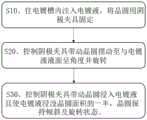
一种电镀工艺预润湿方法,采用以上任一项所述的电镀工艺预润湿系统,包括如下步骤:An electroplating process pre-wetting method adopts the electroplating process pre-wetting system described in any one of the above, comprising the steps of:
S10、往电镀槽内注入电镀液,将晶圆用阴极夹具固定;S10. Inject the electroplating solution into the electroplating tank, and fix the wafer with the cathode clamp;
S20、控制阴极夹具带动晶圆摆动至与电镀液液面呈角度并旋转;S20, controlling the cathode fixture to drive the wafer to swing to form an angle with the electroplating liquid level and rotate;
S30、控制阴极夹具带动晶圆以倾斜及旋转的姿态浸入电镀液且使电镀液浸没晶圆面积的一半。S30 , controlling the cathode fixture to drive the wafer to immerse in the electroplating solution in a tilted and rotated posture, and make the electroplating solution immerse half of the area of the wafer.
本技术方案中,通过采用以上方法步骤设计,利用阴极夹具控制晶圆在带有斜度的状态下以旋转动作浸入电镀槽的电镀液中,晶圆的部分区域浸入电镀液,部分区域未浸入,通过电镀液与晶圆表面的接触以及利用电镀液本身的表面张力,使电镀液不断冲刷晶圆浸入电镀液的那部分区域,结合晶圆与电镀液液面相对倾斜,晶圆表面孔隙中的气泡将不断被电镀液所取代,而被电镀液置换出的气体也容易在浮力作用下上升到自由表面破裂而后扩散至空气当中,实现彻底排除气泡的目的,此举有效保障了后续的电镀效果。In this technical solution, by adopting the design of the above method steps, the cathode fixture is used to control the wafer to immerse in the electroplating bath in the electroplating bath in a rotating motion with a slope, part of the wafer is immersed in the electroplating solution, and part of the area is not immersed. , through the contact between the electroplating solution and the surface of the wafer and the use of the surface tension of the electroplating solution itself, the electroplating solution continuously flushes the area where the wafer is immersed in the electroplating solution. The air bubbles will be continuously replaced by the electroplating solution, and the gas displaced by the electroplating solution will easily rise to the free surface under the action of buoyancy, break and then diffuse into the air to achieve the purpose of completely eliminating the air bubbles, which effectively guarantees the subsequent electroplating Effect.
优选地,步骤S30中,在使电源模块未供电的情况下,控制阴极夹具带动晶圆以倾斜及旋转的姿态浸入电镀液。Preferably, in step S30, when the power supply module is not powered, the cathode clamp is controlled to drive the wafer to immerse in the electroplating solution in a tilted and rotated posture.
本技术方案中,通过采用以上方法步骤设计,当电源模块处于未供电状态,阳极组件和阴极夹具之间将不会产生任何电场效应,由此使得晶圆以倾斜及旋转姿态浸入电镀液时,气泡能够非常顺利的排出。In this technical solution, by adopting the design of the above method steps, when the power module is in the unpowered state, no electric field effect will be generated between the anode assembly and the cathode fixture, so that when the wafer is immersed in the electroplating solution in a tilted and rotated posture, Air bubbles can escape very smoothly.
优选地,在步骤S30之后,在步骤S30之后,还包括步骤S40、保持晶圆在电镀液中的倾斜及旋转姿态,控制电源模块按照预设参数向阳极组件供电。Preferably, after step S30, after step S30, step S40 is further included, maintaining the tilt and rotation posture of the wafer in the electroplating solution, and controlling the power supply module to supply power to the anode assembly according to preset parameters.
本技术方案中,通过采用以上方法步骤设计,如认为晶圆表面图形结构存在孔道深度较深或开孔较小等情况,在晶圆倾斜旋转的过程中,可使电源模块处于供电状态,从而使阳极组件和阴极夹具产生电势差,电镀槽中电镀液的金属离子将游至阴极夹具上夹持的晶圆,从而实现使金属离子更好的注入到微小的孔道中或者到达深孔底部的目的,在配合晶圆倾斜旋转排气泡的情况下,此举可更好提升后续电镀的整体填充良率,大大改善电镀金属层面的粗糙度问题,提升电镀质量。In this technical solution, through the design of the above method and steps, if it is considered that the surface pattern structure of the wafer has a deep hole depth or a small hole, etc., the power module can be in the power supply state during the tilting rotation of the wafer, so that A potential difference is generated between the anode assembly and the cathode fixture, and the metal ions in the plating solution in the electroplating tank will swim to the wafer held on the cathode fixture, so that the metal ions can be better injected into the tiny channels or reach the bottom of the deep hole , In the case of cooperating with the tilting and rotating of the wafer to remove air bubbles, this can better improve the overall filling yield of subsequent electroplating, greatly improve the roughness of the electroplated metal layer, and improve the quality of electroplating.
优选地,步骤S20中,控制阴极夹具带动晶圆摆动至与电镀液液面呈4~5°。Preferably, in step S20, the cathode clamp is controlled to drive the wafer to swing to an angle of 4-5° to the surface of the electroplating solution.
本技术方案中,通过采用以上方法步骤,当晶圆相对电镀液液面摆动的角度范围介于4°至5°之间时,气泡的排除效果佳,且在该角度范围内,夹持晶圆的阴极夹具倾斜幅度较小,由此不会使驱动装置产生过多负担,如此可简化驱动装置的结构。In this technical solution, by adopting the above method steps, when the angle range of the swing of the wafer relative to the electroplating liquid surface is between 4° and 5°, the effect of removing air bubbles is good, and within this angle range, the clamping wafer The circular cathode holder has a small inclination, so that the drive device is not overburdened, which simplifies the structure of the drive device.
优选地,步骤S20中,控制阴极夹具带动晶圆绕晶圆轴线往相同方向作360°旋转。Preferably, in step S20, the cathode clamp is controlled to drive the wafer to rotate 360° around the wafer axis in the same direction.
本技术方案中,通过采用以上方法步骤,使晶圆绕其轴线作360°旋转,可以保证晶圆表面的各个区域均能够与电镀液接触并被刷走气泡,同时,晶圆往相同方向重复作旋转动作,可避免水流因扰动从而产生气泡。In this technical solution, by adopting the above method steps, the wafer is rotated 360° around its axis, which can ensure that each area of the wafer surface can be in contact with the electroplating solution and the bubbles will be brushed away. At the same time, the wafer will repeat in the same direction. The rotating action can avoid the generation of air bubbles due to the disturbance of the water flow.
优选地,步骤S20中,晶圆旋转的速度范围为0~100rpm。Preferably, in step S20, the speed range of the wafer rotation is 0-100 rpm.
本技术方案中,晶圆的转速控制在0至100rpm之间时,一方面可以保证能够利用电镀液的液体张力将晶圆表面孔隙中的气泡带出,另一方面避免转速过高而增加对晶圆及阴极夹具的负荷,提高设备的可靠性。In this technical solution, when the speed of the wafer is controlled between 0 and 100rpm, on the one hand, it can ensure that the liquid tension of the electroplating solution can be used to take out the air bubbles in the pores on the surface of the wafer; The load on the wafer and cathode fixture improves the reliability of the equipment.
与现有技术相比,本发明具有如下的有益效果:Compared with the prior art, the present invention has the following beneficial effects:
1、本发明提供的电镀工艺预润湿系统及方法,利用电镀液与晶圆表面的接触以及电镀液本身的表面张力,结合晶圆的倾斜及旋转状态,让电镀液冲击晶圆表面图形结构,从而使晶圆表面孔隙中的气泡不断被电镀液所取代,这避免了后续电镀空洞现象的产生,实现了优异的电镀效果。1. The electroplating process pre-wetting system and method provided by the present invention utilizes the contact between the electroplating solution and the wafer surface and the surface tension of the electroplating solution itself, combined with the tilt and rotation state of the wafer, to allow the electroplating solution to impact the pattern structure of the wafer surface , so that the bubbles in the pores of the wafer surface are continuously replaced by the electroplating solution, which avoids the occurrence of subsequent electroplating voids and achieves excellent electroplating effects.
2、本发明提供的电镀工艺预润湿系统及方法,在阴极夹具带动晶圆以倾斜及旋转姿态浸入电镀液时,可使阳极组件和阴极夹具不处于导通状态,由此使得阳极组件和阴极夹具之间不产生任何电场效应,使气泡得以顺利排出。2. The electroplating process pre-wetting system and method provided by the present invention, when the cathode fixture drives the wafer to immerse in the electroplating solution in a tilted and rotated posture, can make the anode assembly and the cathode fixture not in the conduction state, thereby making the anode assembly and There is no electric field effect between the cathode clamps, so that the bubbles can be discharged smoothly.
3、本发明提供的电镀工艺预润湿系统及方法,在晶圆表面图形结构存在孔道深度较深或开孔较小等情况时,在晶圆于电镀槽内倾斜旋转的过程中,可使阳极组件和阴极夹具处于导通状态,从而使阳极组件和阴极夹具产生电势差,使得金属离子更好的注入到晶圆表面微小的孔道中或者到达深孔底部,提升后续电镀的整体填充良率。3. The electroplating process pre-wetting system and method provided by the present invention, when the surface pattern structure of the wafer has a deeper hole depth or a smaller opening, can make the wafer tilt and rotate in the electroplating tank. The anode assembly and the cathode fixture are in a conducting state, so that a potential difference is generated between the anode assembly and the cathode fixture, so that metal ions are better injected into the tiny pores on the wafer surface or reach the bottom of the deep hole, improving the overall filling yield of subsequent electroplating.
附图说明Description of drawings
通过阅读参照以下附图对非限制性实施例所作的详细描述,本发明的其它特征、目的和优点将会变得更明显:Other characteristics, objects and advantages of the present invention will become more apparent by reading the detailed description of non-limiting embodiments made with reference to the following drawings:
图1为本发明所述电镀工艺预润湿系统的结构示意图一;Fig. 1 is the structural representation one of electroplating process pre-wetting system of the present invention;
图2为本发明所述电镀工艺预润湿系统的结构示意图二;Fig. 2 is the structural representation two of electroplating process pre-wetting system of the present invention;
图3为晶圆摆动至倾斜姿态的结构示意图;FIG. 3 is a schematic structural diagram of a wafer swinging to a tilted attitude;
图4为晶圆以倾斜姿态旋转的结构示意图;FIG. 4 is a schematic structural diagram of a wafer rotating in a tilted attitude;
图5为晶圆摆动至与电镀液液面呈角度并旋转的结构示意图;Fig. 5 is a schematic diagram of the structure of the wafer swinging to an angle with the electroplating liquid surface and rotating;
图6为晶圆以倾斜及旋转姿态浸入电镀液且仅一半面积浸入的结构示意图;Figure 6 is a schematic diagram of the structure of the wafer immersed in the electroplating solution in a tilted and rotated posture and only half of the area is immersed;
图7为电镀液浸没晶圆一半面积的结构示意图;FIG. 7 is a schematic diagram of the structure of half the area of the wafer immersed in the electroplating solution;
图8为本发明所述电镀工艺预润湿方法的流程框图。Fig. 8 is a flow chart of the pre-wetting method of the electroplating process according to the present invention.
图中示出:The figure shows:
100-电镀工艺预润湿系统100- Electroplating process pre-wetting system
1-晶圆;1 - Wafer;
2-阴极夹具;2 - cathode fixture;
3-驱动装置;3- drive device;
4-电镀槽;4- electroplating tank;
5-电镀液5- Plating solution
具体实施方式Detailed ways
为使本申请实施例的目的、技术方案和优点更加清楚,下面将结合本申请实施例中的附图,对本申请实施例中的技术方案进行清楚、完整地描述,显然,所描述的实施例是本申请一部分实施例,而不是全部的实施例。通常在此处附图中描述和示出的本申请实施例的组件可以以各种不同的配置来布置和设计。In order to make the purposes, technical solutions and advantages of the embodiments of the present application clearer, the technical solutions in the embodiments of the present application will be clearly and completely described below in conjunction with the drawings in the embodiments of the present application. Obviously, the described embodiments It is a part of the embodiments of this application, not all of them. The components of the embodiments of the application generally described and illustrated in the figures herein may be arranged and designed in a variety of different configurations.
因此,以下对在附图中提供的本申请的实施例的详细描述并非旨在限制要求保护的本申请的范围,而是仅仅表示本申请的选定实施例。基于本申请中的实施例,本领域普通技术人员在没有作出创造性劳动前提下所获得的所有其他实施例,都属于本申请保护的范围。Accordingly, the following detailed description of the embodiments of the application provided in the accompanying drawings is not intended to limit the scope of the claimed application, but merely represents selected embodiments of the application. Based on the embodiments in this application, all other embodiments obtained by persons of ordinary skill in the art without creative efforts fall within the protection scope of this application.
应注意到:相似的标号和字母在下面的附图中表示类似项,因此,一旦某一项在一个附图中被定义,则在随后的附图中不需要对其进行进一步定义和解释。此外,本申请中所有方向性指示(诸如上、下、左、右、前、后、底…)仅用于解释在某一特定姿态(如附图所示)下各部件之间的相对位置关系、运动情况等,如果该特定姿态发生改变时,则该方向性指示也相应地随之改变。进一步地,在申请中涉及“第一”、“第二”等的描述仅用于描述目的,而不能理解为指示或暗示其相对重要性或者隐含指明所指示的技术特征的数量。It should be noted that like numerals and letters denote similar items in the following figures, therefore, once an item is defined in one figure, it does not require further definition and explanation in subsequent figures. In addition, all directional indications (such as up, down, left, right, front, back, bottom...) in this application are only used to explain the relative position between the various parts in a certain posture (as shown in the drawing) relationship, motion, etc., if the particular pose changes, the directional indication changes accordingly. Further, the descriptions involving "first", "second", etc. in the application are only for descriptive purposes, and should not be understood as indicating or implying their relative importance or implicitly indicating the number of indicated technical features.
第1实施例first embodiment
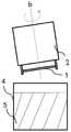
如图1至图7所示,本实施例提供一种电镀工艺预润湿系统100,包括驱动装置3、阴极夹具2以及电镀槽4;电镀槽4内注入有电镀液5;驱动装置3与阴极夹具2连接,驱动装置3用于驱动阴极夹具2平移、旋转或翻转;阴极夹具2用于夹持晶圆1,阴极夹具2可在驱动装置3的控制下带动晶圆1以倾斜及旋转姿态浸入电镀液5且使电镀液5浸没晶圆1面积的一半。As shown in Figures 1 to 7, the present embodiment provides an electroplating process
具体地,如图1所示,将晶圆1固定在阴极夹具2上,并使晶圆1处理面朝下,阴极夹具2与驱动装置3连接,驱动装置3驱动阴极夹具2产生位移,以带动晶圆1沿特定方向移动。如图2所示,驱动装置3也可通过阴极夹具2控制晶圆1以a线为转轴摆动或以b线为转轴旋转。所谓摆动,如图3所示,是指晶圆1在驱动装置3的控制下摆动至与水平面呈任意角度;所谓旋转,如图4所示,是指晶圆1在驱动装置3的控制下围绕其轴线旋转。Specifically, as shown in FIG. 1, the
本实施例通过采用以上的结构设计,如图5所示,可控制晶圆1摆动至与电镀液5液面呈角度并旋转,进一步地,如图6所示,可控制晶圆1以倾斜且旋转的姿态浸入电镀液5,且将晶圆1表面的一半区域浸入电镀液5,一半区域未浸入,由于电镀液5本身有粘度,且晶圆1表面也并非绝对光滑而是具有一定粗糙度,在此情况下,当晶圆1以一定转速旋转时,电镀液5会被晶圆1表面带起并填充至晶圆1表面的孔隙,结合晶圆1与电镀液5液面相对倾斜,且晶圆1仅部分区域浸入电镀液5而非全部浸入,被电镀液5置换出的气体容易在浮力作用下上升到自由表面破裂而后扩散至空气当中,由此实现排出晶圆1表面气泡的目的,同时,由于晶圆1仅一半面积浸没于电镀液5中,一半面积露出电镀液5,结合晶圆1的旋转动作,可以保证晶圆1表面的各个区域均与电镀液5接触且接触的时间相同。In this embodiment, by adopting the above structural design, as shown in FIG. 5, the
作为优选的实施方式,本实施例提供的电镀工艺预润湿系统100还包括控制器和与控制器电连接的电源模块,电镀槽4内设置有阳极组件,电源模块的正极电连接阳极组件,电源模块的负极电连接阴极夹具2;控制器用于发送供电指令至电源模块,电源模块用于在接受到供电指令时,向阳极组件供电。控制器向电源模块发出供电指令的目的不仅仅是控制电源模块供电与否,还可以是对电源模块的供电时间、供电时长、供电电流以及供电电压等进行控制,因此供电指令可以包括以下参数中的任意一种或多种:向阳极组件供电的电流值、向阳极组件供电的电压值、向阳极组件供电的时间以及向阳极组件供电的时长。As a preferred embodiment, the electroplating process
本实施例通过以上的结构设计,使得可通过控制电源模块的供电与否实现更好的气泡排出效果以及电镀效果。具体地,一方面,在阴极夹具2带动晶圆1以倾斜及旋转姿态浸入电镀液5时,可使电源模块处于未供电状态,由此使得阳极组件和阴极夹具2之间不产生任何电场效应,保障气泡顺利排出;另一方面,在晶圆1于电镀槽4内保持倾斜及旋转的过程中,可根据所需情况使电源模块处于供电状态或不供电状态,如认为晶圆1表面图形结构存在孔道深度较深或开孔较小等情况,在晶圆1倾斜及旋转的过程中,可使电源模块处于供电状态,从而使阳极组件和阴极夹具2产生电势差,电镀槽4中电镀液5的金属离子将游至阴极夹具2上夹持的晶圆1,从而实现使金属离子更好的注入到微小的孔道中或者到达深孔底部的目的,在配合晶圆1倾斜旋转排气泡的情况下,此举可更好提升后续电镀的整体填充良率,大大改善电镀金属层面的粗糙度问题,提升电镀质量。In this embodiment, through the above structural design, it is possible to achieve better air bubble discharge effect and electroplating effect by controlling the power supply of the power module. Specifically, on the one hand, when the
作为优选的实施方式,如图1所示,电镀槽4设置于阴极夹具2的正下方,由此使得驱动装置3仅须通过简单的升降动作即可将晶圆1浸入电镀液5内,这一方面简化了驱动装置3的结构,使整体设备的体积得以减小;另一方面,使阴极夹具2花费最少的时间和移动距离就能够带动晶圆1浸入电镀液5中,从而在保证气泡排出效果的同时,节约时间,简化操作流程。此外,驱动装置3可包括机械手,机械手与阴极夹具2连接,利用机械手来移动阴极夹具2,能够更为快速、便捷的使阴极夹具2带动晶圆1移动。As a preferred embodiment, as shown in FIG. 1, the
本实施例提供的电镀工艺预润湿系统,通过以上的结构设计,利用电镀液与晶圆表面的接触以及电镀液本身的表面张力,结合晶圆的倾斜及旋转状态,使电镀液冲击晶圆表面图形结构,从而使晶圆表面孔隙中的气泡不断被电镀液所取代,这避免了后续电镀空洞现象的产生,实现了优异的电镀效果。The electroplating process pre-wetting system provided in this embodiment, through the above structural design, uses the contact between the electroplating solution and the surface of the wafer and the surface tension of the electroplating solution itself, combined with the tilt and rotation state of the wafer, to make the electroplating solution impact the wafer The surface pattern structure, so that the bubbles in the pores of the wafer surface are continuously replaced by the electroplating solution, which avoids the occurrence of subsequent electroplating voids and achieves excellent electroplating effects.
第2实施例2nd embodiment
如图8所示,本实施例提供一种电镀工艺预润湿方法,采用第1实施例所述的电镀工艺预润湿系统100,包括如下步骤:As shown in FIG. 8, this embodiment provides a method for pre-wetting the electroplating process, using the electroplating process
S10、往电镀槽4内注入电镀液5,将晶圆1用阴极夹具2固定;S10. Inject the
S20、控制阴极夹具2带动晶圆1摆动至与电镀液5液面呈角度并旋转;S20, controlling the
S30、控制阴极夹具2带动晶圆1以倾斜及旋转的姿态浸入电镀液5且使电镀液5浸没晶圆1面积的一半。S30 , controlling the
本实施例利用阴极夹具2控制晶圆1在带有斜度的状态下以旋转动作浸入电镀槽4的电镀液5中,晶圆1的部分区域浸入电镀液5,部分区域未浸入,通过电镀液5与晶圆1表面的接触以及利用电镀液5本身的表面张力,使电镀液5不断冲刷晶圆1浸入电镀液5的那部分区域,结合晶圆1与电镀液5液面相对倾斜,晶圆1表面孔隙中的气泡将不断被电镀液5所取代,而被电镀液5置换出的气体也容易在浮力作用下上升到自由表面破裂而后扩散至空气当中,实现彻底排除气泡的目的。In this embodiment, the
作为一种优选的实施方式,在实施步骤S30时,即晶圆1以倾斜及旋转姿态浸入电镀液5时,使电源模块处于未供电状态,由此使得阳极组件和阴极夹具2之间不会产生任何电场效应,使得气泡能够非常顺利的排出。As a preferred embodiment, when implementing step S30, that is, when the
作为一种优选的实施方式,在步骤S30之后,还包括步骤S40,即晶圆1以倾斜及旋转姿态浸入电镀液5后,保持晶圆1在电镀液5中的倾斜及旋转姿态,在此过程中,使用者可根据实际需要选择是否使电源模块供电。倘若晶圆1表面图形结构存在孔道深度较深或开孔较小等情况,则可控制电源模块处于供电状态,从而使阳极组件和阴极夹具2产生电势差,电镀槽4中电镀液5的金属离子将游至阴极夹具2上夹持的晶圆1,从而实现使金属离子更好的注入到微小的孔道中或者到达深孔底部的目的,在配合晶圆1倾斜旋转排气泡的情况下,此举可更好提升后续电镀的整体填充良率,大大改善电镀金属层面的粗糙度问题,提升电镀质量。As a preferred embodiment, after step S30, step S40 is also included, that is, after the
就晶圆1的倾斜状态来说,作为优选的实施方式,控制阴极夹具2带动晶圆1摆动至与电镀液5液面呈4~5°,即使晶圆1相对于电镀液5液面向上或向下倾斜4~5°,由此在保证气泡排除效果的同时,使得夹持晶圆1的阴极夹具2倾斜幅度较小,由此不会使驱动装置3产生过多负担,如此可简化驱动装置3的结构。而就晶圆1的旋转状态来说,作为优选的实施方式,控制阴极夹具2带动晶圆1绕晶圆1中心点往相同方向作360°旋转,在晶圆1的一半面积浸入电镀液5、一半面积露出电镀液5的情况下,晶圆1作360°旋转,可以保证晶圆1表面的各个区域均能够与电镀液5接触并被刷走气泡,同时,晶圆1往相同方向重复作旋转动作,可避免水流因扰动从而产生气泡;就晶圆1的旋转速度来说,可将其控制在0~100rpm的转速之间,以在保证利用电镀液5的液体张力将晶圆1表面孔隙中的气泡带出的同时,避免转速过高而增加对晶圆1及阴极夹具2的负荷,提高设备的可靠性。As far as the tilt state of the
本实施例提供的电镀工艺预润湿系统及方法,利用电镀液5与晶圆1表面的接触以及电镀液5本身的表面张力,结合晶圆1的倾斜及旋转状态,让电镀液5冲击晶圆1表面图形结构,从而使晶圆1表面孔隙中的气泡不断被电镀液所取代,这避免了后续电镀空洞现象的产生,实现了优异的电镀效果。同时,在阴极夹具2带动晶圆1以倾斜及旋转姿态浸入电镀液5时,本实施例可通过控制电源模块不供电的方式使得阳极组件和阴极夹具2之间不产生任何电场效应,使气泡得以顺利排出。此外,在晶圆1表面图形结构存在孔道深度较深或开孔较小等情况时,在晶圆1于电镀槽4内倾斜旋转的过程中,本实施例可控制电源模块供电,从而使阳极组件和阴极夹具2产生电势差,使得金属离子更好的注入到晶圆1表面微小的孔道中或者到达深孔底部,提升后续电镀的整体填充良率。The electroplating process pre-wetting system and method provided in this embodiment utilizes the contact between the
以上对本发明的具体实施例进行了描述,通过上述的说明内容,相关工作人员完全可以在不偏离本项发明技术思想的范围内,进行多样的变更以及修改。The specific embodiments of the present invention have been described above. Through the above description, relevant workers can make various changes and modifications within the scope of not departing from the technical idea of the present invention.
Claims (4)
Priority Applications (1)
| Application Number | Priority Date | Filing Date | Title |
|---|---|---|---|
| CN202111319339.4ACN113862746B (en) | 2021-11-09 | 2021-11-09 | Pre-wetting system and method for electroplating process |
Applications Claiming Priority (1)
| Application Number | Priority Date | Filing Date | Title |
|---|---|---|---|
| CN202111319339.4ACN113862746B (en) | 2021-11-09 | 2021-11-09 | Pre-wetting system and method for electroplating process |
Publications (2)
| Publication Number | Publication Date |
|---|---|
| CN113862746A CN113862746A (en) | 2021-12-31 |
| CN113862746Btrue CN113862746B (en) | 2023-02-17 |
Family
ID=78987651
Family Applications (1)
| Application Number | Title | Priority Date | Filing Date |
|---|---|---|---|
| CN202111319339.4AActiveCN113862746B (en) | 2021-11-09 | 2021-11-09 | Pre-wetting system and method for electroplating process |
Country Status (1)
| Country | Link |
|---|---|
| CN (1) | CN113862746B (en) |
Families Citing this family (3)
| Publication number | Priority date | Publication date | Assignee | Title |
|---|---|---|---|---|
| CN114577178B (en)* | 2022-03-17 | 2023-11-24 | 新阳硅密(上海)半导体技术有限公司 | Electroplating head level detection device and method |
| CN115418700B (en)* | 2022-09-06 | 2025-08-29 | 无锡琨圣智能装备股份有限公司 | Electroplating tank for realizing inclined electroplating |
| CN116065222B (en)* | 2023-03-09 | 2023-06-13 | 苏州智程半导体科技股份有限公司 | Wafer electroplating clamp moving device |
Citations (7)
| Publication number | Priority date | Publication date | Assignee | Title |
|---|---|---|---|---|
| TW475224B (en)* | 2001-01-11 | 2002-02-01 | Applied Materials Inc | Method to remove bubble on wafer surface during electroplating process |
| JP2002080995A (en)* | 2000-09-08 | 2002-03-22 | Hitachi Ltd | Method of manufacturing semiconductor device |
| CN101459050A (en)* | 2007-12-14 | 2009-06-17 | 盛美半导体设备(上海)有限公司 | Method and apparatus for metallic layer front wafer surface presoaking for electrochemical or chemical deposition |
| CN103021933A (en)* | 2012-09-18 | 2013-04-03 | 上海集成电路研发中心有限公司 | Method for preprocessing wafer groove before chemical electroplating process |
| CN105529282A (en)* | 2014-09-29 | 2016-04-27 | 盛美半导体设备(上海)有限公司 | A semiconductor pre-wetting device and method |
| CN111146126A (en)* | 2020-01-21 | 2020-05-12 | 新阳硅密(上海)半导体技术有限公司 | Pre-wetting equipment, pre-wetting system, and pre-wetting method for wafer pre-wetting |
| CN112877741A (en)* | 2021-01-13 | 2021-06-01 | 硅密芯镀(海宁)半导体技术有限公司 | Bubble removing method and wafer electroplating equipment |
Family Cites Families (3)
| Publication number | Priority date | Publication date | Assignee | Title |
|---|---|---|---|---|
| JP3695703B2 (en)* | 2001-10-25 | 2005-09-14 | 株式会社日立製作所 | Electroplating method, electroplating apparatus and semiconductor device manufacturing method and manufacturing apparatus |
| JP2005002448A (en)* | 2003-06-13 | 2005-01-06 | Tokyo Electron Ltd | Electroless plating equipment and electroless plating method |
| US20100320081A1 (en)* | 2009-06-17 | 2010-12-23 | Mayer Steven T | Apparatus for wetting pretreatment for enhanced damascene metal filling |
- 2021
- 2021-11-09CNCN202111319339.4Apatent/CN113862746B/enactiveActive
Patent Citations (7)
| Publication number | Priority date | Publication date | Assignee | Title |
|---|---|---|---|---|
| JP2002080995A (en)* | 2000-09-08 | 2002-03-22 | Hitachi Ltd | Method of manufacturing semiconductor device |
| TW475224B (en)* | 2001-01-11 | 2002-02-01 | Applied Materials Inc | Method to remove bubble on wafer surface during electroplating process |
| CN101459050A (en)* | 2007-12-14 | 2009-06-17 | 盛美半导体设备(上海)有限公司 | Method and apparatus for metallic layer front wafer surface presoaking for electrochemical or chemical deposition |
| CN103021933A (en)* | 2012-09-18 | 2013-04-03 | 上海集成电路研发中心有限公司 | Method for preprocessing wafer groove before chemical electroplating process |
| CN105529282A (en)* | 2014-09-29 | 2016-04-27 | 盛美半导体设备(上海)有限公司 | A semiconductor pre-wetting device and method |
| CN111146126A (en)* | 2020-01-21 | 2020-05-12 | 新阳硅密(上海)半导体技术有限公司 | Pre-wetting equipment, pre-wetting system, and pre-wetting method for wafer pre-wetting |
| CN112877741A (en)* | 2021-01-13 | 2021-06-01 | 硅密芯镀(海宁)半导体技术有限公司 | Bubble removing method and wafer electroplating equipment |
Also Published As
| Publication number | Publication date |
|---|---|
| CN113862746A (en) | 2021-12-31 |
Similar Documents
| Publication | Publication Date | Title |
|---|---|---|
| CN113862746B (en) | Pre-wetting system and method for electroplating process | |
| CN102534714B (en) | Electro-plating method | |
| US9677188B2 (en) | Electrofill vacuum plating cell | |
| JP2002506488A (en) | Electrochemical deposition system and substrate electroplating method | |
| KR20140075636A (en) | Electrofill vacuum plating cell | |
| JPH0617291A (en) | Metal plating device | |
| JP2002220692A (en) | Plating equipment and method | |
| US20110108415A1 (en) | Apparatus and method for plating a substrate | |
| US20070158202A1 (en) | Plating apparatus and method for controlling plating solution | |
| JP3534605B2 (en) | Substrate plating equipment | |
| HK1246371A1 (en) | Electroplating device and method for wafer | |
| US20080057211A1 (en) | Methods for plating and fabrication apparatus thereof | |
| CN112877741A (en) | Bubble removing method and wafer electroplating equipment | |
| US20030051995A1 (en) | Plating device and plating method | |
| US20040206628A1 (en) | Electrical bias during wafer exit from electrolyte bath | |
| US20070181441A1 (en) | Method and apparatus for electropolishing | |
| JP3698596B2 (en) | Plating apparatus and plating method | |
| KR101278711B1 (en) | Apparatus and method for plating semiconductor wafers | |
| JP2014029028A (en) | Plating method | |
| KR101621813B1 (en) | Apparatus For Plating Having Function For Draining Bubble On The Surface Of Work | |
| US20040192066A1 (en) | Method for immersing a substrate | |
| KR101170765B1 (en) | Apparatus and method for plating substrate | |
| CN215940848U (en) | Surface exhaust equipment for single-chip immersion type wet treatment process | |
| CN100449710C (en) | Method for electrochemically plating semiconductor wafers and plating apparatus therefor | |
| JP2009293088A (en) | Electroplating device and electroplating method |
Legal Events
| Date | Code | Title | Description |
|---|---|---|---|
| PB01 | Publication | ||
| PB01 | Publication | ||
| SE01 | Entry into force of request for substantive examination | ||
| SE01 | Entry into force of request for substantive examination | ||
| GR01 | Patent grant | ||
| GR01 | Patent grant | ||
| CP03 | Change of name, title or address | Address after:Building 8, No. 3600 Sixian Road, Songjiang District, Shanghai, 201600 Patentee after:Xindongwei (Shanghai) Semiconductor Technology Co.,Ltd. Country or region after:China Address before:No. 3600 Sixian Road, Songjiang District, Shanghai Patentee before:XINYANG GUIMI (SHANGHAI) SEMICONDUCTOR TECHNOLOGY CO.,LTD. Country or region before:China | |
| CP03 | Change of name, title or address |