CN113820893B - Display panel and display device - Google Patents
Display panel and display deviceDownload PDFInfo
- Publication number
- CN113820893B CN113820893BCN202010559623.8ACN202010559623ACN113820893BCN 113820893 BCN113820893 BCN 113820893BCN 202010559623 ACN202010559623 ACN 202010559623ACN 113820893 BCN113820893 BCN 113820893B
- Authority
- CN
- China
- Prior art keywords
- sub
- pixel
- display
- distance
- upper edge
- Prior art date
- Legal status (The legal status is an assumption and is not a legal conclusion. Google has not performed a legal analysis and makes no representation as to the accuracy of the status listed.)
- Active
Links
Images


Classifications
- G—PHYSICS
- G02—OPTICS
- G02F—OPTICAL DEVICES OR ARRANGEMENTS FOR THE CONTROL OF LIGHT BY MODIFICATION OF THE OPTICAL PROPERTIES OF THE MEDIA OF THE ELEMENTS INVOLVED THEREIN; NON-LINEAR OPTICS; FREQUENCY-CHANGING OF LIGHT; OPTICAL LOGIC ELEMENTS; OPTICAL ANALOGUE/DIGITAL CONVERTERS
- G02F1/00—Devices or arrangements for the control of the intensity, colour, phase, polarisation or direction of light arriving from an independent light source, e.g. switching, gating or modulating; Non-linear optics
- G02F1/01—Devices or arrangements for the control of the intensity, colour, phase, polarisation or direction of light arriving from an independent light source, e.g. switching, gating or modulating; Non-linear optics for the control of the intensity, phase, polarisation or colour
- G02F1/13—Devices or arrangements for the control of the intensity, colour, phase, polarisation or direction of light arriving from an independent light source, e.g. switching, gating or modulating; Non-linear optics for the control of the intensity, phase, polarisation or colour based on liquid crystals, e.g. single liquid crystal display cells
- G02F1/133—Constructional arrangements; Operation of liquid crystal cells; Circuit arrangements
- G02F1/1333—Constructional arrangements; Manufacturing methods
- G02F1/1335—Structural association of cells with optical devices, e.g. polarisers or reflectors
- G02F1/133509—Filters, e.g. light shielding masks
- G02F1/133512—Light shielding layers, e.g. black matrix
- G—PHYSICS
- G02—OPTICS
- G02F—OPTICAL DEVICES OR ARRANGEMENTS FOR THE CONTROL OF LIGHT BY MODIFICATION OF THE OPTICAL PROPERTIES OF THE MEDIA OF THE ELEMENTS INVOLVED THEREIN; NON-LINEAR OPTICS; FREQUENCY-CHANGING OF LIGHT; OPTICAL LOGIC ELEMENTS; OPTICAL ANALOGUE/DIGITAL CONVERTERS
- G02F1/00—Devices or arrangements for the control of the intensity, colour, phase, polarisation or direction of light arriving from an independent light source, e.g. switching, gating or modulating; Non-linear optics
- G02F1/01—Devices or arrangements for the control of the intensity, colour, phase, polarisation or direction of light arriving from an independent light source, e.g. switching, gating or modulating; Non-linear optics for the control of the intensity, phase, polarisation or colour
- G02F1/13—Devices or arrangements for the control of the intensity, colour, phase, polarisation or direction of light arriving from an independent light source, e.g. switching, gating or modulating; Non-linear optics for the control of the intensity, phase, polarisation or colour based on liquid crystals, e.g. single liquid crystal display cells
- G02F1/133—Constructional arrangements; Operation of liquid crystal cells; Circuit arrangements
- G02F1/136—Liquid crystal cells structurally associated with a semi-conducting layer or substrate, e.g. cells forming part of an integrated circuit
- G02F1/1362—Active matrix addressed cells
- G02F1/136286—Wiring, e.g. gate line, drain line
- G—PHYSICS
- G02—OPTICS
- G02F—OPTICAL DEVICES OR ARRANGEMENTS FOR THE CONTROL OF LIGHT BY MODIFICATION OF THE OPTICAL PROPERTIES OF THE MEDIA OF THE ELEMENTS INVOLVED THEREIN; NON-LINEAR OPTICS; FREQUENCY-CHANGING OF LIGHT; OPTICAL LOGIC ELEMENTS; OPTICAL ANALOGUE/DIGITAL CONVERTERS
- G02F1/00—Devices or arrangements for the control of the intensity, colour, phase, polarisation or direction of light arriving from an independent light source, e.g. switching, gating or modulating; Non-linear optics
- G02F1/01—Devices or arrangements for the control of the intensity, colour, phase, polarisation or direction of light arriving from an independent light source, e.g. switching, gating or modulating; Non-linear optics for the control of the intensity, phase, polarisation or colour
- G02F1/13—Devices or arrangements for the control of the intensity, colour, phase, polarisation or direction of light arriving from an independent light source, e.g. switching, gating or modulating; Non-linear optics for the control of the intensity, phase, polarisation or colour based on liquid crystals, e.g. single liquid crystal display cells
- G02F1/133—Constructional arrangements; Operation of liquid crystal cells; Circuit arrangements
- G02F1/1333—Constructional arrangements; Manufacturing methods
- G02F1/1335—Structural association of cells with optical devices, e.g. polarisers or reflectors
- G02F1/133509—Filters, e.g. light shielding masks
- G02F1/133514—Colour filters
- G—PHYSICS
- G02—OPTICS
- G02F—OPTICAL DEVICES OR ARRANGEMENTS FOR THE CONTROL OF LIGHT BY MODIFICATION OF THE OPTICAL PROPERTIES OF THE MEDIA OF THE ELEMENTS INVOLVED THEREIN; NON-LINEAR OPTICS; FREQUENCY-CHANGING OF LIGHT; OPTICAL LOGIC ELEMENTS; OPTICAL ANALOGUE/DIGITAL CONVERTERS
- G02F1/00—Devices or arrangements for the control of the intensity, colour, phase, polarisation or direction of light arriving from an independent light source, e.g. switching, gating or modulating; Non-linear optics
- G02F1/01—Devices or arrangements for the control of the intensity, colour, phase, polarisation or direction of light arriving from an independent light source, e.g. switching, gating or modulating; Non-linear optics for the control of the intensity, phase, polarisation or colour
- G02F1/13—Devices or arrangements for the control of the intensity, colour, phase, polarisation or direction of light arriving from an independent light source, e.g. switching, gating or modulating; Non-linear optics for the control of the intensity, phase, polarisation or colour based on liquid crystals, e.g. single liquid crystal display cells
- G02F1/133—Constructional arrangements; Operation of liquid crystal cells; Circuit arrangements
- G02F1/1333—Constructional arrangements; Manufacturing methods
- G02F1/1343—Electrodes
- G02F1/134309—Electrodes characterised by their geometrical arrangement
- G02F1/134345—Subdivided pixels, e.g. for grey scale or redundancy
- G—PHYSICS
- G02—OPTICS
- G02F—OPTICAL DEVICES OR ARRANGEMENTS FOR THE CONTROL OF LIGHT BY MODIFICATION OF THE OPTICAL PROPERTIES OF THE MEDIA OF THE ELEMENTS INVOLVED THEREIN; NON-LINEAR OPTICS; FREQUENCY-CHANGING OF LIGHT; OPTICAL LOGIC ELEMENTS; OPTICAL ANALOGUE/DIGITAL CONVERTERS
- G02F1/00—Devices or arrangements for the control of the intensity, colour, phase, polarisation or direction of light arriving from an independent light source, e.g. switching, gating or modulating; Non-linear optics
- G02F1/01—Devices or arrangements for the control of the intensity, colour, phase, polarisation or direction of light arriving from an independent light source, e.g. switching, gating or modulating; Non-linear optics for the control of the intensity, phase, polarisation or colour
- G02F1/13—Devices or arrangements for the control of the intensity, colour, phase, polarisation or direction of light arriving from an independent light source, e.g. switching, gating or modulating; Non-linear optics for the control of the intensity, phase, polarisation or colour based on liquid crystals, e.g. single liquid crystal display cells
- G02F1/133—Constructional arrangements; Operation of liquid crystal cells; Circuit arrangements
- G02F1/1333—Constructional arrangements; Manufacturing methods
- G02F1/1343—Electrodes
- G02F1/134309—Electrodes characterised by their geometrical arrangement
- G02F1/134363—Electrodes characterised by their geometrical arrangement for applying an electric field parallel to the substrate, i.e. in-plane switching [IPS]
- G—PHYSICS
- G02—OPTICS
- G02F—OPTICAL DEVICES OR ARRANGEMENTS FOR THE CONTROL OF LIGHT BY MODIFICATION OF THE OPTICAL PROPERTIES OF THE MEDIA OF THE ELEMENTS INVOLVED THEREIN; NON-LINEAR OPTICS; FREQUENCY-CHANGING OF LIGHT; OPTICAL LOGIC ELEMENTS; OPTICAL ANALOGUE/DIGITAL CONVERTERS
- G02F1/00—Devices or arrangements for the control of the intensity, colour, phase, polarisation or direction of light arriving from an independent light source, e.g. switching, gating or modulating; Non-linear optics
- G02F1/01—Devices or arrangements for the control of the intensity, colour, phase, polarisation or direction of light arriving from an independent light source, e.g. switching, gating or modulating; Non-linear optics for the control of the intensity, phase, polarisation or colour
- G02F1/13—Devices or arrangements for the control of the intensity, colour, phase, polarisation or direction of light arriving from an independent light source, e.g. switching, gating or modulating; Non-linear optics for the control of the intensity, phase, polarisation or colour based on liquid crystals, e.g. single liquid crystal display cells
- G02F1/133—Constructional arrangements; Operation of liquid crystal cells; Circuit arrangements
- G02F1/136—Liquid crystal cells structurally associated with a semi-conducting layer or substrate, e.g. cells forming part of an integrated circuit
- G02F1/1362—Active matrix addressed cells
- G02F1/136227—Through-hole connection of the pixel electrode to the active element through an insulation layer
- G—PHYSICS
- G02—OPTICS
- G02F—OPTICAL DEVICES OR ARRANGEMENTS FOR THE CONTROL OF LIGHT BY MODIFICATION OF THE OPTICAL PROPERTIES OF THE MEDIA OF THE ELEMENTS INVOLVED THEREIN; NON-LINEAR OPTICS; FREQUENCY-CHANGING OF LIGHT; OPTICAL LOGIC ELEMENTS; OPTICAL ANALOGUE/DIGITAL CONVERTERS
- G02F1/00—Devices or arrangements for the control of the intensity, colour, phase, polarisation or direction of light arriving from an independent light source, e.g. switching, gating or modulating; Non-linear optics
- G02F1/01—Devices or arrangements for the control of the intensity, colour, phase, polarisation or direction of light arriving from an independent light source, e.g. switching, gating or modulating; Non-linear optics for the control of the intensity, phase, polarisation or colour
- G02F1/13—Devices or arrangements for the control of the intensity, colour, phase, polarisation or direction of light arriving from an independent light source, e.g. switching, gating or modulating; Non-linear optics for the control of the intensity, phase, polarisation or colour based on liquid crystals, e.g. single liquid crystal display cells
- G02F1/133—Constructional arrangements; Operation of liquid crystal cells; Circuit arrangements
- G02F1/136—Liquid crystal cells structurally associated with a semi-conducting layer or substrate, e.g. cells forming part of an integrated circuit
- G02F1/1362—Active matrix addressed cells
- G02F1/1368—Active matrix addressed cells in which the switching element is a three-electrode device
- G—PHYSICS
- G02—OPTICS
- G02F—OPTICAL DEVICES OR ARRANGEMENTS FOR THE CONTROL OF LIGHT BY MODIFICATION OF THE OPTICAL PROPERTIES OF THE MEDIA OF THE ELEMENTS INVOLVED THEREIN; NON-LINEAR OPTICS; FREQUENCY-CHANGING OF LIGHT; OPTICAL LOGIC ELEMENTS; OPTICAL ANALOGUE/DIGITAL CONVERTERS
- G02F1/00—Devices or arrangements for the control of the intensity, colour, phase, polarisation or direction of light arriving from an independent light source, e.g. switching, gating or modulating; Non-linear optics
- G02F1/01—Devices or arrangements for the control of the intensity, colour, phase, polarisation or direction of light arriving from an independent light source, e.g. switching, gating or modulating; Non-linear optics for the control of the intensity, phase, polarisation or colour
- G02F1/13—Devices or arrangements for the control of the intensity, colour, phase, polarisation or direction of light arriving from an independent light source, e.g. switching, gating or modulating; Non-linear optics for the control of the intensity, phase, polarisation or colour based on liquid crystals, e.g. single liquid crystal display cells
- G02F1/133—Constructional arrangements; Operation of liquid crystal cells; Circuit arrangements
- G02F1/1333—Constructional arrangements; Manufacturing methods
- G02F1/133345—Insulating layers
- G—PHYSICS
- G02—OPTICS
- G02F—OPTICAL DEVICES OR ARRANGEMENTS FOR THE CONTROL OF LIGHT BY MODIFICATION OF THE OPTICAL PROPERTIES OF THE MEDIA OF THE ELEMENTS INVOLVED THEREIN; NON-LINEAR OPTICS; FREQUENCY-CHANGING OF LIGHT; OPTICAL LOGIC ELEMENTS; OPTICAL ANALOGUE/DIGITAL CONVERTERS
- G02F1/00—Devices or arrangements for the control of the intensity, colour, phase, polarisation or direction of light arriving from an independent light source, e.g. switching, gating or modulating; Non-linear optics
- G02F1/01—Devices or arrangements for the control of the intensity, colour, phase, polarisation or direction of light arriving from an independent light source, e.g. switching, gating or modulating; Non-linear optics for the control of the intensity, phase, polarisation or colour
- G02F1/13—Devices or arrangements for the control of the intensity, colour, phase, polarisation or direction of light arriving from an independent light source, e.g. switching, gating or modulating; Non-linear optics for the control of the intensity, phase, polarisation or colour based on liquid crystals, e.g. single liquid crystal display cells
- G02F1/133—Constructional arrangements; Operation of liquid crystal cells; Circuit arrangements
- G02F1/1333—Constructional arrangements; Manufacturing methods
- G02F1/1337—Surface-induced orientation of the liquid crystal molecules, e.g. by alignment layers
- G02F1/133707—Structures for producing distorted electric fields, e.g. bumps, protrusions, recesses, slits in pixel electrodes
- G—PHYSICS
- G02—OPTICS
- G02F—OPTICAL DEVICES OR ARRANGEMENTS FOR THE CONTROL OF LIGHT BY MODIFICATION OF THE OPTICAL PROPERTIES OF THE MEDIA OF THE ELEMENTS INVOLVED THEREIN; NON-LINEAR OPTICS; FREQUENCY-CHANGING OF LIGHT; OPTICAL LOGIC ELEMENTS; OPTICAL ANALOGUE/DIGITAL CONVERTERS
- G02F1/00—Devices or arrangements for the control of the intensity, colour, phase, polarisation or direction of light arriving from an independent light source, e.g. switching, gating or modulating; Non-linear optics
- G02F1/01—Devices or arrangements for the control of the intensity, colour, phase, polarisation or direction of light arriving from an independent light source, e.g. switching, gating or modulating; Non-linear optics for the control of the intensity, phase, polarisation or colour
- G02F1/13—Devices or arrangements for the control of the intensity, colour, phase, polarisation or direction of light arriving from an independent light source, e.g. switching, gating or modulating; Non-linear optics for the control of the intensity, phase, polarisation or colour based on liquid crystals, e.g. single liquid crystal display cells
- G02F1/133—Constructional arrangements; Operation of liquid crystal cells; Circuit arrangements
- G02F1/1333—Constructional arrangements; Manufacturing methods
- G02F1/1343—Electrodes
- G02F1/13439—Electrodes characterised by their electrical, optical, physical properties; materials therefor; method of making
- G—PHYSICS
- G02—OPTICS
- G02F—OPTICAL DEVICES OR ARRANGEMENTS FOR THE CONTROL OF LIGHT BY MODIFICATION OF THE OPTICAL PROPERTIES OF THE MEDIA OF THE ELEMENTS INVOLVED THEREIN; NON-LINEAR OPTICS; FREQUENCY-CHANGING OF LIGHT; OPTICAL LOGIC ELEMENTS; OPTICAL ANALOGUE/DIGITAL CONVERTERS
- G02F1/00—Devices or arrangements for the control of the intensity, colour, phase, polarisation or direction of light arriving from an independent light source, e.g. switching, gating or modulating; Non-linear optics
- G02F1/01—Devices or arrangements for the control of the intensity, colour, phase, polarisation or direction of light arriving from an independent light source, e.g. switching, gating or modulating; Non-linear optics for the control of the intensity, phase, polarisation or colour
- G02F1/13—Devices or arrangements for the control of the intensity, colour, phase, polarisation or direction of light arriving from an independent light source, e.g. switching, gating or modulating; Non-linear optics for the control of the intensity, phase, polarisation or colour based on liquid crystals, e.g. single liquid crystal display cells
- G02F1/133—Constructional arrangements; Operation of liquid crystal cells; Circuit arrangements
- G02F1/136—Liquid crystal cells structurally associated with a semi-conducting layer or substrate, e.g. cells forming part of an integrated circuit
- G02F1/13606—Liquid crystal cells structurally associated with a semi-conducting layer or substrate, e.g. cells forming part of an integrated circuit having means for reducing parasitic capacitance
- G—PHYSICS
- G02—OPTICS
- G02F—OPTICAL DEVICES OR ARRANGEMENTS FOR THE CONTROL OF LIGHT BY MODIFICATION OF THE OPTICAL PROPERTIES OF THE MEDIA OF THE ELEMENTS INVOLVED THEREIN; NON-LINEAR OPTICS; FREQUENCY-CHANGING OF LIGHT; OPTICAL LOGIC ELEMENTS; OPTICAL ANALOGUE/DIGITAL CONVERTERS
- G02F2201/00—Constructional arrangements not provided for in groups G02F1/00 - G02F7/00
- G02F2201/40—Arrangements for improving the aperture ratio
- G—PHYSICS
- G02—OPTICS
- G02F—OPTICAL DEVICES OR ARRANGEMENTS FOR THE CONTROL OF LIGHT BY MODIFICATION OF THE OPTICAL PROPERTIES OF THE MEDIA OF THE ELEMENTS INVOLVED THEREIN; NON-LINEAR OPTICS; FREQUENCY-CHANGING OF LIGHT; OPTICAL LOGIC ELEMENTS; OPTICAL ANALOGUE/DIGITAL CONVERTERS
- G02F2201/00—Constructional arrangements not provided for in groups G02F1/00 - G02F7/00
- G02F2201/52—RGB geometrical arrangements
Landscapes
- Physics & Mathematics (AREA)
- Nonlinear Science (AREA)
- General Physics & Mathematics (AREA)
- Chemical & Material Sciences (AREA)
- Crystallography & Structural Chemistry (AREA)
- Mathematical Physics (AREA)
- Optics & Photonics (AREA)
- Engineering & Computer Science (AREA)
- Microelectronics & Electronic Packaging (AREA)
- Geometry (AREA)
- Spectroscopy & Molecular Physics (AREA)
- Liquid Crystal (AREA)
- Devices For Indicating Variable Information By Combining Individual Elements (AREA)
Abstract
Description
Translated fromChinese技术领域technical field
本发明涉及但不限于显示技术领域,具体涉及一种显示面板和显示装置。The present invention relates to but not limited to the field of display technology, and specifically relates to a display panel and a display device.
背景技术Background technique
液晶显示装置(Liquid Crystal Display,简称LCD)具有体积小、功耗低、无辐射等特点,已得到迅速发展。液晶显示面板包括对盒(CELL)的薄膜晶体管阵列(Thin FilmTransistor,简称TFT)基板和彩膜(Color Filter,简称CF)基板,液晶(Liquid Crystal,简称LC)分子设置在阵列基板和彩膜基板之间,通过控制公共电极和像素电极来形成驱动液晶偏转的电场,实现灰阶显示。A Liquid Crystal Display (LCD for short) has the characteristics of small size, low power consumption, and no radiation, and has been rapidly developed. The liquid crystal display panel includes a thin film transistor array (Thin Film Transistor, referred to as TFT) substrate and a color filter (Color Filter, referred to as CF) substrate of the cell (CELL), and liquid crystal (Liquid Crystal, referred to as LC) molecules are arranged on the array substrate and the color filter substrate. In between, by controlling the common electrode and the pixel electrode to form an electric field that drives the deflection of the liquid crystal to realize grayscale display.
随着TFT-LCD技术的成熟,大尺寸、超大尺寸高分辨率液晶显示装置近年来得到迅速发展,市场份额逐渐增加。随着液晶显示装置尺寸增大,横纹和暗态漏光等不良问题比较严重,对产品品质和良率造成较大影响。With the maturity of TFT-LCD technology, large-size and ultra-large-size high-resolution liquid crystal display devices have developed rapidly in recent years, and their market share has gradually increased. As the size of the liquid crystal display device increases, problems such as horizontal stripes and light leakage in the dark state are more serious, which have a great impact on product quality and yield.
发明内容Contents of the invention
以下是对本文详细描述的主题的概述。本概述并非是为了限制权利要求的保护范围。The following is an overview of the topics described in detail in this article. This summary is not intended to limit the scope of the claims.
本发明实施例所要解决的技术问题是,提供一种显示面板和显示装置,以解决现有显示装置存在横纹和暗态漏光等问题。The technical problem to be solved by the embodiments of the present invention is to provide a display panel and a display device to solve the problems of horizontal stripes and dark state light leakage in the existing display devices.
为了解决上述技术问题,本发明实施例提供了一种显示面板,包括相对设置的第一基板和第二基板;In order to solve the above technical problems, an embodiment of the present invention provides a display panel, including a first substrate and a second substrate oppositely arranged;
所述第一基板包括由M条栅线和N对数据线交叉限定出的M*N个子像素,每对数据线包括第一数据线和第二数据线,所述子像素包括薄膜晶体管和像素电极;第m显示行中,所有子像素的薄膜晶体管与第m条栅线连接;第n显示列中,奇数显示行中子像素的薄膜晶体管与第n对数据线的第一数据线连接,偶数显示行中子像素的薄膜晶体管与第n对数据线的第二数据线连接;或者,第n显示列中,偶数显示行中子像素的薄膜晶体管与第n对数据线的第一数据线连接,奇数显示行中子像素的薄膜晶体管与第n对数据线的第二数据线连接;M和N为大于或等于1的正整数,m=1,2,……,M,n=1,2,……,N;The first substrate includes M*N sub-pixels defined by intersections of M gate lines and N pairs of data lines, each pair of data lines includes a first data line and a second data line, and the sub-pixels include a thin film transistor and a pixel Electrodes; in the mth display row, the thin film transistors of all subpixels are connected to the m gate line; in the nth display column, the thin film transistors of the subpixels in odd display rows are connected to the first data line of the nth pair of data lines, The thin film transistors of the sub-pixels in the even-numbered display rows are connected to the second data line of the n-th pair of data lines; or, in the n-th display column, the thin-film transistors of the sub-pixels in the even-numbered display rows are connected to the first data line of the n-th pair of data lines Connection, the thin film transistors of the sub-pixels in odd display rows are connected to the second data line of the nth pair of data lines; M and N are positive integers greater than or equal to 1, m=1, 2, ..., M, n=1 ,2,...,N;
所述第二基板包括与所述子像素一一对应的M*N个滤光单元,相邻的滤光单元之间设置有黑矩阵,所述黑矩阵包括位于相邻显示行之间的遮挡行和位于相邻显示列之间的遮挡列;The second substrate includes M*N filter units one-to-one corresponding to the sub-pixels, and a black matrix is arranged between adjacent filter units, and the black matrix includes blocking elements located between adjacent display rows. Rows and occluded columns between adjacent displayed columns;
在所述数据线的延伸方向,位于第k显示行与第k+1显示行之间的遮挡行具有第一宽度,位于第k+1显示行与第k+2显示行之间的遮挡行具有第二宽度,所述第一宽度不等于所述第二宽度。In the extending direction of the data lines, the shielding row between the kth display row and the k+1th display row has a first width, and the shielding row between the k+1th display row and the k+2th display row Having a second width, the first width is not equal to the second width.
在一些可能的实现方式中,第m显示行中的多个子像素包括周期性排布的第一子像素、第二子像素和第三子像素;位于第k显示行与第k+1显示行之间的遮挡行中,所述遮挡行包括位于第k显示行内的上边缘和位于第k+1显示行内的下边缘;所述上边缘包括位于第k显示行的第一子像素内的第一上边缘、位于第k显示行的第二子像素内的第二上边缘和位于第k显示行的第三子像素内的第三上边缘,所述下边缘包括位于第k+1显示行的第一子像素内的第一下边缘、位于第k+1显示行的第二子像素内的第二下边缘和位于第k+1显示行的第三子像素内的第三下边缘;位于第k+1显示行与第k+2显示行之间的遮挡行中,所述遮挡行包括位于第k+1显示行内的上边缘和位于第k+2显示行内的下边缘;所述上边缘包括位于第k+1显示行的第一子像素内的第四上边缘、位于第k+1显示行的第二子像素内的第五上边缘和位于第k+1显示行的第三子像素内的第六上边缘,所述下边缘包括位于第k+2显示行的第一子像素内的第四下边缘、位于第k+2显示行的第二子像素内的第五下边缘和位于第k+2显示行的第三子像素内的第六下边缘;在所述数据线的延伸方向,所述第一上边缘与第一下边缘之间的距离为第一距离,所述第二上边缘与第二下边缘之间的距离为第二距离,所述第三上边缘与第三下边缘之间的距离为第三距离,所述第四上边缘与第四下边缘之间的距离为第四距离,所述第五上边缘与第五下边缘之间的距离为第五距离,所述第六上边缘与第六下边缘之间的距离为第六距离;所述第一宽度不等于第二宽度包括如下任意一种或多种:所述第一距离小于第四距离,所述第二距离小于第五距离,所述第三距离大于第六距离。In some possible implementations, the multiple sub-pixels in the mth display row include periodically arranged first sub-pixels, second sub-pixels and third sub-pixels; In the shading row between, the shading row includes an upper edge located in the kth display row and a lower edge located in the k+1th display row; the upper edge includes the first subpixel located in the kth display row An upper edge, a second upper edge located in the second subpixel of the kth display row, and a third upper edge located in the third subpixel of the kth display row, the lower edge includes the k+1th display row The first lower edge in the first sub-pixel of , the second lower edge in the second sub-pixel of the k+1th display row, and the third lower edge in the third sub-pixel of the k+1th display row; In the shading row between the k+1th display row and the k+2th display row, the shading row includes an upper edge in the k+1th display row and a lower edge in the k+2th display row; the The upper edge includes a fourth upper edge located in the first subpixel of the k+1th display row, a fifth upper edge located in the second subpixel of the k+1th display row, and a fifth upper edge located in the k+1th display row The sixth upper edge in the three sub-pixels, the lower edge includes the fourth lower edge in the first sub-pixel of the k+2th display row, the fifth lower edge in the second sub-pixel of the k+2th display row The lower edge and the sixth lower edge located in the third sub-pixel of the k+2th display row; in the extending direction of the data line, the distance between the first upper edge and the first lower edge is the first distance , the distance between the second upper edge and the second lower edge is the second distance, the distance between the third upper edge and the third lower edge is the third distance, and the fourth upper edge and the fourth The distance between the lower edges is the fourth distance, the distance between the fifth upper edge and the fifth lower edge is the fifth distance, and the distance between the sixth upper edge and the sixth lower edge is the sixth distance ; The first width being not equal to the second width includes any one or more of the following: the first distance is smaller than the fourth distance, the second distance is smaller than the fifth distance, and the third distance is larger than the sixth distance.
在一些可能的实现方式中,所述第一距离与第四距离之差为10μm~20μm,所述第二距离与第五距离之差为10μm~20μm,所述第三距离与第六距离之差为1μm~5μm。In some possible implementation manners, the difference between the first distance and the fourth distance is 10 μm-20 μm, the difference between the second distance and the fifth distance is 10 μm-20 μm, and the difference between the third distance and the sixth distance The difference is 1 μm to 5 μm.
在一些可能的实现方式中,所述第三距离大于第一距离,所述第三距离大于第二距离。In some possible implementation manners, the third distance is greater than the first distance, and the third distance is greater than the second distance.
在一些可能的实现方式中,所述第三距离与第一距离之差为10μm~35μm,所述第三距离与第二距离之差为10μm~35μm。In some possible implementation manners, the difference between the third distance and the first distance is 10 μm˜35 μm, and the difference between the third distance and the second distance is 10 μm˜35 μm.
在一些可能的实现方式中,所述第六距离大于第四距离,所述第六距离大于第五距离。In some possible implementation manners, the sixth distance is greater than the fourth distance, and the sixth distance is greater than the fifth distance.
在一些可能的实现方式中,所述第六距离与第四距离之差为10μm~20μm,所述第六距离与第五距离之差为10μm~20μm。In some possible implementation manners, the difference between the sixth distance and the fourth distance is 10 μm˜20 μm, and the difference between the sixth distance and the fifth distance is 10 μm˜20 μm.
在一些可能的实现方式中,位于第k显示行的第一子像素内的遮挡行设置有第一凸起,所述第一凸起设置在所述第一上边缘上,沿着远离所述第一下边缘的方向延伸;位于第k显示行的第二子像素内的遮挡行设置有第二凸起,所述第二凸起设置在所述第二上边缘上,所述第二凸起沿着远离所述第二下边缘的方向延伸。In some possible implementation manners, the shielding row located in the first sub-pixel of the kth display row is provided with a first protrusion, and the first protrusion is disposed on the first upper edge along the The direction of the first lower edge extends; the shielding row located in the second sub-pixel of the kth display row is provided with a second protrusion, the second protrusion is arranged on the second upper edge, and the second protrusion extending along a direction away from the second lower edge.
在一些可能的实现方式中,在所述栅线的延伸方向,所述第一凸起位于所述第一子像素中设置薄膜晶体管的一侧,所述第二凸起位于所述第二子像素中设置薄膜晶体管的一侧。In some possible implementation manners, in the extending direction of the gate line, the first protrusion is located on the side where the thin film transistor is disposed in the first sub-pixel, and the second protrusion is located on the side of the second sub-pixel A side where a thin film transistor is provided in a pixel.
在一些可能的实现方式中,所述第一凸起和第二凸起的形状包括矩形或梯形。In some possible implementation manners, the shapes of the first protrusion and the second protrusion include a rectangle or a trapezoid.
在一些可能的实现方式中,在所述数据线的延伸方向,所述第一凸起包括第一凸起上边缘,所述第二凸起包括第二凸起上边缘,所述第一凸起上边缘与所述第一上边缘之间的距离为10μm~20μm,所述第二凸起上边缘与所述第二上边缘之间的距离为10μm~20μm。In some possible implementation manners, in the extending direction of the data line, the first protrusion includes a first protrusion upper edge, the second protrusion includes a second protrusion upper edge, and the first protrusion The distance between the raised upper edge and the first upper edge is 10 μm˜20 μm, and the distance between the second raised upper edge and the second upper edge is 10 μm˜20 μm.
在一些可能的实现方式中,在所述数据线的延伸方向,所述第三上边缘与所述第一上边缘之间的距离大于所述第一凸起上边缘与所述第一上边缘之间的距离,所述第三上边缘与所述第二上边缘之间的距离大于所述第二凸起上边缘与所述第二上边缘之间的距离。In some possible implementation manners, in the extending direction of the data line, the distance between the third upper edge and the first upper edge is greater than the distance between the first raised upper edge and the first upper edge The distance between the third upper edge and the second upper edge is greater than the distance between the second raised upper edge and the second upper edge.
在一些可能的实现方式中,所述第一下边缘、第二下边缘和第三下边缘均为沿所述栅线的延伸方向延伸的平直边缘;所述第四上边缘、第五上边缘和第六上边缘均为沿所述栅线的延伸方向延伸的平直边缘;所述第四下边缘、第五下边缘和第六下边缘上均设置有凸块,所述凸块分别设置在所述第四下边缘、第五下边缘和第六下边缘邻近两侧遮挡列的位置。In some possible implementation manners, the first lower edge, the second lower edge and the third lower edge are all straight edges extending along the extending direction of the grid lines; the fourth upper edge, the fifth upper edge The edge and the sixth upper edge are straight edges extending along the extending direction of the grid lines; the fourth lower edge, the fifth lower edge and the sixth lower edge are all provided with bumps, and the bumps are respectively It is arranged at the position where the fourth lower edge, the fifth lower edge and the sixth lower edge are adjacent to the shielding columns on both sides.
在一些可能的实现方式中,所述凸块包括直角三角形,所述直角三角形的第一直边分别设置在所述第四下边缘、第五下边缘和第六下边缘上,所述直角三角形的第二直边分别设置在所述第四下边缘、第五下边缘和第六下边缘两侧的遮挡列上。In some possible implementation manners, the bump includes a right-angled triangle, and the first straight sides of the right-angled triangle are respectively arranged on the fourth lower edge, the fifth lower edge, and the sixth lower edge, and the right-angled triangle The second straight sides are respectively arranged on the shielding columns on both sides of the fourth lower edge, the fifth lower edge and the sixth lower edge.
在一些可能的实现方式中,所述第一基板包括叠设的第一导电层、第一金属层、第一绝缘层、半导体层、第二金属层、第二绝缘层和第二导电层;所述第一导电层包括设置在每个子像素内的公共电极;所述第一金属层包括栅线和公共电极线、设置在每个子像素内的栅电极和设置在所述第三子像素内的第一连接电极,所述栅线与每个子像素内的栅电极连接,所述公共电极线与每个子像素内的公共电极连接,所述第一连接电极与所述第三子像素的公共电极连接;所述半导体层包括设置在每个子像素内的有源层;所述第二金属层包括第一数据线、第二数据线以及设置在每个子像素内的源电极和漏电极,第k显示行中,每个子像素的源电极与所述第一数据线连接,第k+1显示行中,每个子像素的源电极与所述第二数据线连接,所述源电极与漏电极之间形成导电沟道;所述第二导电层包括设置在每个子像素内的像素电极和设置在所述第三子像素中的第二连接电极,所述像素电极通过过孔与所在子像素的漏电极连接,所述第二连接电极通过过孔分别与第一连接电极和公共电极线连接。In some possible implementation manners, the first substrate includes a stacked first conductive layer, a first metal layer, a first insulating layer, a semiconductor layer, a second metal layer, a second insulating layer, and a second conductive layer; The first conductive layer includes a common electrode arranged in each sub-pixel; the first metal layer includes a gate line and a common electrode line, a gate electrode arranged in each sub-pixel, and a gate electrode arranged in the third sub-pixel The first connection electrode, the gate line is connected to the gate electrode in each sub-pixel, the common electrode line is connected to the common electrode in each sub-pixel, the first connection electrode is connected to the common electrode of the third sub-pixel electrode connection; the semiconductor layer includes an active layer arranged in each sub-pixel; the second metal layer includes a first data line, a second data line and a source electrode and a drain electrode arranged in each sub-pixel, the second In the k display row, the source electrode of each subpixel is connected to the first data line, in the k+1th display row, the source electrode of each subpixel is connected to the second data line, and the source electrode and the drain electrode A conductive channel is formed between them; the second conductive layer includes a pixel electrode disposed in each sub-pixel and a second connection electrode disposed in the third sub-pixel, and the pixel electrode is connected to the sub-pixel by a via hole. The drain electrode is connected to the drain electrode, and the second connection electrode is respectively connected to the first connection electrode and the common electrode line through the via hole.
在一些可能的实现方式中,第k显示行中,所述第一子像素、第二子像素和第三子像素中的公共电极设置有第一公共电极凸起,每个子像素的第一公共电极凸位于所述公共电极邻近第k-1显示行的一侧;所述第三子像素中的公共电极设置有第二公共电极凸起,所述第二公共电极凸起位于所述公共电极邻近下一显示行的一侧,所述第一连接电极设置在所述第二公共电极凸起上。In some possible implementation manners, in the kth display row, the common electrodes in the first subpixel, the second subpixel, and the third subpixel are provided with first common electrode protrusions, and the first common electrode protrusions of each subpixel are The electrode protrusion is located on the side of the common electrode adjacent to the k-1th display row; the common electrode in the third sub-pixel is provided with a second common electrode protrusion, and the second common electrode protrusion is located on the common electrode Adjacent to one side of the next display row, the first connection electrode is disposed on the second common electrode protrusion.
在一些可能的实现方式中,在相邻公共电极线之间的第一间隔区域,所述公共电极线具有第三宽度,在相邻第一间隔区域之间的第二间隔区域,所述公共电极线具有第四宽度,所述第三宽度小于所述第四宽度;在所述第一间隔区域,所述栅线具有第五宽度,在所述第二间隔区域,所述栅线具有第六宽度,所述第五宽度小于所述第六宽度。In some possible implementation manners, in the first spacing area between adjacent common electrode lines, the common electrode line has a third width, and in the second spacing area between adjacent first spacing areas, the common electrode line has a third width. The electrode line has a fourth width, and the third width is smaller than the fourth width; in the first interval region, the gate line has a fifth width, and in the second interval region, the gate line has a fifth width. Six widths, the fifth width is smaller than the sixth width.
在一些可能的实现方式中,所述第一子像素、第二子像素和第三子像素中的栅电极均为矩形状,所述第一子像素和第二子像素中栅电极的长边沿着显示行方向延伸,所述第三子像素中的栅电极的长边沿着显示列方向延伸。In some possible implementation manners, the gate electrodes in the first subpixel, the second subpixel and the third subpixel are all rectangular, and the long edges of the gate electrodes in the first subpixel and the second subpixel are The long side of the gate electrode in the third sub-pixel extends along the display column direction.
在一些可能的实现方式中,所述第二连接电极的一端通过所述第一绝缘层和第二绝缘层上开设的过孔与所述第一连接电极连接,第二连接电极的另一端通过所述第一绝缘层和第二绝缘层上开设的过孔与下一显示行的公共电极线连接。In some possible implementation manners, one end of the second connection electrode is connected to the first connection electrode through a via hole opened on the first insulating layer and the second insulating layer, and the other end of the second connection electrode is connected to the second connection electrode through The via holes opened on the first insulating layer and the second insulating layer are connected to the common electrode lines of the next display row.
在一些可能的实现方式中,每个子像素中,所述像素电极与漏电极的连接区域与所述黑矩阵存在交叠,所述像素电极的边缘区域与黑矩阵存在交叠。In some possible implementation manners, in each sub-pixel, the connection area between the pixel electrode and the drain electrode overlaps with the black matrix, and the edge area of the pixel electrode overlaps with the black matrix.
在一些可能的实现方式中,第k显示行中的多个滤光单元包括周期性排布的第一滤光单元、第二滤光单元和第三滤光单元,所述第一滤光单元对应所述第一子像素,所述第二滤光单元对应所述第二子像素,所述第三滤光单元对应所述第三子像素;所述第一滤光单元包括红色滤光单元,所述第二滤光单元包括绿色滤光单元,所述第三滤光单元包括蓝色滤光单元。In some possible implementation manners, the multiple filter units in the kth display row include periodically arranged first filter units, second filter units, and third filter units, and the first filter units Corresponding to the first sub-pixel, the second filter unit corresponds to the second sub-pixel, and the third filter unit corresponds to the third sub-pixel; the first filter unit includes a red filter unit , the second filter unit includes a green filter unit, and the third filter unit includes a blue filter unit.
本发明实施例还提供了一种显示装置,包括上述的显示面板。An embodiment of the present invention also provides a display device, including the above-mentioned display panel.
本发明实施例提供了一种显示面板和显示装置,通过将奇数显示行和偶数显示行的遮挡行设置成不同宽度,减小了奇数显示行的像素开口率与偶数显示行的像素开口率之间的差异,有效避免了横纹不良和暗态漏光不良。Embodiments of the present invention provide a display panel and a display device. By setting the shading lines of odd-numbered display rows and even-numbered display rows to have different widths, the difference between the pixel aperture ratios of odd-numbered display rows and the pixel aperture ratios of even-numbered display rows is reduced. The difference between them effectively avoids bad horizontal stripes and bad light leakage in dark states.
当然,实施本发明的任一产品或方法并不一定需要同时达到以上所述的所有优点。本发明的其它特征和优点将在随后的说明书实施例中阐述,并且,部分地从说明书实施例中变得显而易见,或者通过实施本发明而了解。本发明实施例的目的和其他优点可通过在说明书、权利要求书以及附图中所特别指出的结构来实现和获得。Of course, implementing any product or method of the present invention does not necessarily need to achieve all the above-mentioned advantages at the same time. Additional features and advantages of the invention will be set forth in the description which follows, and in part will be apparent from the description, or may be learned by practice of the invention. The objectives and other advantages of the embodiments of the present invention can be realized and obtained by the structures particularly pointed out in the description, claims and accompanying drawings.
在阅读并理解了附图和详细描述后,可以明白其他方面。Other aspects will be apparent to others upon reading and understanding the drawings and detailed description.
附图说明Description of drawings
附图用来提供对本公开技术方案的进一步理解,并且构成说明书的一部分,与本公开的实施例一起用于解释本公开的技术方案,并不构成对本公开技术方案的限制。附图中各部件的形状和大小不反映真实比例,目的只是示意说明本公开内容。The accompanying drawings are used to provide a further understanding of the technical solutions of the present disclosure, and constitute a part of the specification, and are used together with the embodiments of the present disclosure to explain the technical solutions of the present disclosure, and do not constitute limitations to the technical solutions of the present disclosure. The shapes and sizes of the various components in the drawings do not reflect true scale, but are only intended to illustrate the present disclosure.
图1为本发明实施例显示面板的结构示意图;FIG. 1 is a schematic structural diagram of a display panel according to an embodiment of the present invention;
图2为本发明实施例一种第一基板的等效电路图;2 is an equivalent circuit diagram of a first substrate according to an embodiment of the present invention;
图3是本发明实施例一种显示面板的俯视图;3 is a top view of a display panel according to an embodiment of the present invention;
图4A为本发明实施例形成第一导电层图案后的示意图;FIG. 4A is a schematic diagram after forming a first conductive layer pattern according to an embodiment of the present invention;
图4B为图4A中A-A向的剖视图;Fig. 4B is a sectional view of A-A direction in Fig. 4A;
图4C为图4A中B-B向的剖视图;Fig. 4C is a cross-sectional view of B-B direction in Fig. 4A;
图5A为本发明实施例形成第一金属层图案后的示意图;FIG. 5A is a schematic diagram after forming a first metal layer pattern according to an embodiment of the present invention;
图5B为图5A中A-A向的剖视图;Fig. 5B is a cross-sectional view of A-A direction in Fig. 5A;
图5C为图5A中B-B向的剖视图;Fig. 5C is a cross-sectional view of B-B direction in Fig. 5A;
图6A为本发明实施例形成半导体层图案后的示意图;FIG. 6A is a schematic diagram after forming a semiconductor layer pattern according to an embodiment of the present invention;
图6B为图6A中A-A向的剖视图;Fig. 6B is a sectional view of A-A direction in Fig. 6A;
图6C为图6A中B-B向的剖视图;Fig. 6C is a cross-sectional view of B-B direction in Fig. 6A;
图7A为本发明实施例形成第二金属层图案后的示意图;FIG. 7A is a schematic diagram of forming a second metal layer pattern according to an embodiment of the present invention;
图7B为图7A中A-A向的剖视图;Fig. 7B is a sectional view of A-A direction in Fig. 7A;
图7C为图7A中B-B向的剖视图;Fig. 7C is a cross-sectional view of B-B direction in Fig. 7A;
图8A为本发明实施例形成第二绝缘层图案后的示意图;FIG. 8A is a schematic diagram after forming a second insulating layer pattern according to an embodiment of the present invention;
图8B为图8A中A-A向的剖视图;Fig. 8B is a sectional view of A-A direction in Fig. 8A;
图8C为图8A中B-B向的剖视图;Fig. 8C is a cross-sectional view of B-B direction in Fig. 8A;
图9A为本发明实施例形成第二导电层图案后的示意图;FIG. 9A is a schematic diagram after forming a second conductive layer pattern according to an embodiment of the present invention;
图9B为图9A中A-A向的剖视图;Fig. 9B is a sectional view of A-A direction in Fig. 9A;
图9C为图9A中B-B向的剖视图;Fig. 9C is a cross-sectional view of B-B direction in Fig. 9A;
图10A为本发明实施例形成黑矩阵图案后的示意图;FIG. 10A is a schematic diagram of forming a black matrix pattern according to an embodiment of the present invention;
图10B为图10A中C-C向的剖视图;Fig. 10B is a sectional view of C-C direction in Fig. 10A;
图10C为图10A中D-D向的剖视图;Figure 10C is a cross-sectional view of D-D in Figure 10A;
图11A为本发明实施例形成滤光单元图案后的示意图;FIG. 11A is a schematic diagram of forming a filter unit pattern according to an embodiment of the present invention;
图11B为图11A中C-C向的剖视图;Fig. 11B is a sectional view of C-C direction in Fig. 11A;
图11C为图11A中D-D向的剖视图;Figure 11C is a cross-sectional view of D-D in Figure 11A;
图12为本发明实施例形成形成显示面板的示意图;12 is a schematic diagram of forming a display panel according to an embodiment of the present invention;
图13为本发明实施例另一种第一基板的等效电路图。FIG. 13 is an equivalent circuit diagram of another first substrate according to an embodiment of the present invention.
附图标记说明:Explanation of reference signs:
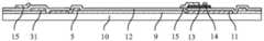
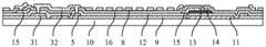
1—第一基板; 2—第二基板; 3—薄膜晶体管;1—first substrate; 2—second substrate; 3—thin film transistor;
4—栅线; 5—公共电极线; 6—第一数据线;4—gate line; 5—common electrode line; 6—first data line;
7—第二数据线; 8—像素电极; 9—公共电极;7—second data line; 8—pixel electrode; 9—common electrode;
10—第一基底; 11—栅电极; 12—第一绝缘层;10—the first substrate; 11—the gate electrode; 12—the first insulating layer;
13—有源层; 14—源电极; 15—漏电极;13—active layer; 14—source electrode; 15—drain electrode;
16—第二绝缘层; 20—第二基底; 21—黑矩阵;16—second insulating layer; 20—second substrate; 21—black matrix;
22—滤光单元; 23—红色滤光单元; 24—绿色滤光单元;22—filter unit; 23—red filter unit; 24—green filter unit;
25—蓝色滤光单元; 31—第一连接电极; 32—第二连接电极;25—blue filter unit; 31—first connection electrode; 32—second connection electrode;
211—遮挡行; 212—遮挡列。211—blocking rows; 212—blocking columns.
具体实施方式detailed description
本文中的实施方式可以以多个不同形式来实施。所属技术领域的普通技术人员可以很容易地理解一个事实,就是实现方式和内容可以在不脱离本公开的宗旨及其范围的条件下被变换为各种各样的形式。因此,本公开不应该被解释为仅限定在下面的实施方式所记载的内容中。在不冲突的情况下,本公开中的实施例及实施例中的特征可以相互任意组合。The embodiments herein may be embodied in many different forms. Those skilled in the art can easily understand the fact that the implementation and contents can be changed into various forms without departing from the gist and scope of the present disclosure. Therefore, the present disclosure should not be interpreted as being limited only to the contents described in the following embodiments. In the case of no conflict, the embodiments in the present disclosure and the features in the embodiments can be combined arbitrarily with each other.
在附图中,有时为了明确起见,可能夸大表示了构成要素的大小、层的厚度或区域。因此,本公开的任意一个实现方式并不一定限定于图中所示尺寸,附图中部件的形状和大小不反映真实比例。此外,附图示意性地示出了理想的例子,本公开的任意一个实现方式不局限于附图所示的形状或数值等。In the drawings, the size of constituent elements, the thickness of layers, or regions may be exaggerated for the sake of clarity. Therefore, any implementation of the present disclosure is not necessarily limited to the dimensions shown in the drawings, and the shapes and sizes of components in the drawings do not reflect true scales. In addition, the drawings schematically show ideal examples, and any implementation of the present disclosure is not limited to the shapes, numerical values, and the like shown in the drawings.
本文中的“第一”、“第二”、“第三”等序数词是为了避免构成要素的混同而设置,而不是为了在数量方面上进行限定的。The ordinal numerals such as "first", "second", and "third" herein are provided to avoid confusion of constituent elements, rather than to limit the quantity.
在本文中,为了方便起见,使用“中部”、“上”、“下”、“前”、“后”、“竖直”、“水平”、“顶”、“底”、“内”、“外”等指示方位或位置关系的词句以参照附图说明构成要素的位置关系,仅是为了便于描述实施方式和简化描述,而不是指示或暗示所指的装置或元件必须具有特定的方位、以特定的方位构造和操作,因此不能理解为对本公开的限制。构成要素的位置关系可根据描述的构成要素的方向进行适当地改变。因此,不局限于在文中说明的词句,根据情况可以适当地更换。In this article, for convenience, the terms "middle", "upper", "lower", "front", "rear", "vertical", "horizontal", "top", "bottom", "inner", Words such as "external" and other words indicating orientation or positional relationship are used to illustrate the positional relationship of constituent elements with reference to the drawings, which are only for the convenience of describing the embodiment and simplifying the description, rather than indicating or implying that the referred device or element must have a specific orientation, constructed and operative in a particular orientation and therefore should not be construed as limiting the present disclosure. The positional relationship of the constituent elements can be appropriately changed according to the directions of the constituent elements described. Therefore, it is not limited to the words and phrases described in the text, and may be appropriately replaced according to circumstances.
在本文中,除非另有明确的规定和限定,术语“安装”、“相连”、“连接”应做广义理解。例如,可以是固定连接,或可拆卸连接,或一体地连接;可以是机械连接,或电连接;可以是直接相连,或通过中间件间接相连,或两个元件内部的连通。对于本领域的普通技术人员而言,可以根据情况理解上述术语在本公开中的含义。In this article, the terms "installation", "connection" and "connection" should be interpreted in a broad sense unless otherwise clearly specified and limited. For example, it may be a fixed connection, or a detachable connection, or an integral connection; it may be a mechanical connection, or an electrical connection; it may be a direct connection, or an indirect connection through an intermediate piece, or an internal communication between two components. Those of ordinary skill in the art can understand the meanings of the above terms in the present disclosure according to the situation.
在本文中,晶体管是指至少包括栅电极、漏电极以及源电极这三个端子的元件。晶体管在漏电极(或称漏电极端子、漏区域或漏电极)与源电极(或称源电极端子、源区域或源电极)之间具有沟道区域,并且电流能够流过漏电极、沟道区域以及源电极。在本文中,沟道区域是指电流主要流过的区域。Herein, a transistor refers to an element including at least three terminals of a gate electrode, a drain electrode, and a source electrode. The transistor has a channel region between the drain electrode (or drain electrode terminal, drain region, or drain electrode) and source electrode (or source electrode terminal, source region, or source electrode), and current can flow through the drain electrode, channel area as well as the source electrode. Herein, the channel region refers to a region through which current mainly flows.
在本文中,第一极可以为漏电极、第二极可以为源电极,或者第一极可以为源电极、第二极可以为漏电极。在使用极性相反的晶体管的情况或电路工作中的电流方向变化的情况下,“源电极”及“漏电极”的功能有时可以互相调换。因此,在本文中,“源电极”和“漏电极”可以互相调换。Herein, the first electrode may be a drain electrode and the second electrode may be a source electrode, or the first electrode may be a source electrode and the second electrode may be a drain electrode. When using transistors with opposite polarities or when the current direction changes during circuit operation, the functions of the "source electrode" and "drain electrode" may be interchanged. Therefore, herein, "source electrode" and "drain electrode" may be interchanged.
在本文中,“电连接”包括构成要素通过具有某种电作用的元件连接在一起的情况。“具有某种电作用的元件”只要可以进行连接的构成要素间的电信号的授受,就对其没有特别的限制。“具有某种电作用的元件”例如可以是电极或布线,或者是晶体管等开关元件,或者是电阻器、电感器或电容器等其它功能元件等。Herein, "electrically connected" includes the case where constituent elements are connected together through an element having some kind of electrical action. The "element having some kind of electrical action" is not particularly limited as long as it can transmit and receive electrical signals between connected components. The "element having some kind of electrical function" may be, for example, an electrode or a wiring, or a switching element such as a transistor, or other functional elements such as a resistor, an inductor, or a capacitor.
在本文中,“平行”是指两条直线形成的角度为-10°以上且10°以下的状态,因此,也包括该角度为-5°以上且5°以下的状态。另外,“垂直”是指两条直线形成的角度为80°以上且100°以下的状态,因此,也包括85°以上且95°以下的角度的状态。Herein, "parallel" refers to a state where the angle formed by two straight lines is -10° to 10°, and therefore includes a state where the angle is -5° to 5°. In addition, "perpendicular" means a state in which the angle formed by two straight lines is 80° to 100°, and therefore also includes an angle of 85° to 95°.
在本文中,“膜”和“层”可以相互调换。例如,有时可以将“导电层”换成为“导电膜”。与此同样,有时可以将“绝缘膜”换成为“绝缘层”。Herein, "film" and "layer" are interchangeable. For example, "conductive layer" may sometimes be replaced with "conductive film". Similarly, "insulating film" may sometimes be replaced with "insulating layer".
本文中的“约”,是指不严格限定界限,允许工艺和测量误差范围内的数值。"About" herein refers to a numerical value that is not strictly limited, and is within the range of process and measurement errors.
现有液晶显示装置通常采用逐行逐列的方式进行扫描,时序控制电路(T-CON)控制显示装置的子像素按照从左到右、从上到下的顺序逐行逐列进行开启。对于大尺寸、超大尺寸液晶显示装置,由于栅线和数据线的数量增加,栅线和数据线的长度也增加,当扫描频率不变时,子像素的有效充电时间大大缩短。为确保大尺寸、超大尺寸高分辨率液晶显示装置的充电率,现有像素结构通常采用栅线双侧驱动和双数据线结构,称之为2G2D驱动。采用2G2D驱动时,一显示行的薄膜晶体管设置在第一数据线的右侧,相邻的另一显示行的薄膜晶体管设置在第二数据线的左侧。经本申请发明人研究发现,相邻两显示行中薄膜晶体管的位置不同,使得相邻两显示行的子像素存在像素开口率差异,像素开口率差异不仅导致横纹不良,而且在阵列基板与彩膜基板错位时会导致暗态漏光不良。Existing liquid crystal display devices usually scan row by row and column by row, and the timing control circuit (T-CON) controls the sub-pixels of the display device to turn on row by row and column by row from left to right and from top to bottom. For large-size and ultra-large-size liquid crystal display devices, due to the increase in the number of gate lines and data lines, the length of the gate lines and data lines also increases. When the scanning frequency remains unchanged, the effective charging time of sub-pixels is greatly shortened. In order to ensure the charging rate of large-size, ultra-large-size and high-resolution liquid crystal display devices, the existing pixel structure usually adopts a gate line double-side drive and a double data line structure, which is called 2G2D drive. When 2G2D driving is adopted, the thin film transistors of one display row are arranged on the right side of the first data line, and the thin film transistors of another adjacent display row are arranged on the left side of the second data line. The inventors of the present application found that the positions of the thin film transistors in two adjacent display lines are different, so that there is a difference in the pixel aperture ratio of the sub-pixels in the two adjacent display rows. When the color filter substrate is misaligned, it will cause poor light leakage in the dark state.
为了解决现有显示装置存在横纹和暗态漏光等问题,本发明实施例提供了一种显示面板。本发明实施例显示面板包括相对设置的第一基板和第二基板;所述第一基板包括由M条栅线和N对数据线交叉限定出的M*N个子像素,每对数据线包括第一数据线和第二数据线,所述子像素包括薄膜晶体管和像素电极;第m显示行中,所有子像素的薄膜晶体管与第m条栅线连接;第n显示列中,奇数显示行中子像素的薄膜晶体管与第n对数据线的第一数据线连接,偶数显示行中子像素的薄膜晶体管与第n对数据线的第二数据线连接;或者,第n显示列中,偶数显示行中子像素的薄膜晶体管与第n对数据线的第一数据线连接,奇数显示行中子像素的薄膜晶体管与第n对数据线的第二数据线连接;M和N为大于或等于1的正整数,m=1,2,……,M,n=1,2,……,N;In order to solve the problems of horizontal stripes and dark state light leakage in existing display devices, an embodiment of the present invention provides a display panel. The display panel in the embodiment of the present invention includes a first substrate and a second substrate oppositely arranged; the first substrate includes M*N sub-pixels defined by crossing M gate lines and N pairs of data lines, and each pair of data lines includes the first A data line and a second data line, the sub-pixels include thin-film transistors and pixel electrodes; in the mth display row, the thin-film transistors of all sub-pixels are connected to the m-th gate line; in the nth display column, in the odd-numbered display row The thin film transistor of the sub-pixel is connected to the first data line of the n-th pair of data lines, and the thin-film transistor of the sub-pixel in the even-numbered display row is connected to the second data line of the n-th pair of data lines; or, in the n-th display column, the even-numbered display The thin-film transistors of the sub-pixels in the row are connected to the first data line of the n-th pair of data lines, and the thin-film transistors of the sub-pixels in the odd-numbered display rows are connected to the second data line of the n-th pair of data lines; M and N are greater than or equal to 1 positive integers, m=1, 2,..., M, n=1, 2,..., N;
所述第二基板包括与所述子像素一一对应的M*N个滤光单元,相邻的滤光单元之间设置有黑矩阵,所述黑矩阵包括位于相邻显示行之间的遮挡行和位于相邻显示列之间的遮挡列;The second substrate includes M*N filter units one-to-one corresponding to the sub-pixels, and a black matrix is arranged between adjacent filter units, and the black matrix includes blocking elements located between adjacent display rows. Rows and occluded columns between adjacent displayed columns;
在所述数据线的延伸方向,位于第k显示行与第k+1显示行之间的遮挡行具有第一宽度,位于第k+1显示行与第k+2显示行之间的遮挡行具有第二宽度,所述第一宽度不等于所述第二宽度。In the extending direction of the data lines, the shielding row between the kth display row and the k+1th display row has a first width, and the shielding row between the k+1th display row and the k+2th display row Having a second width, the first width is not equal to the second width.
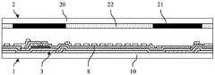
图1为本发明实施例显示面板的结构示意图。如图1所示,显示面板包括相对设置的第一基板1和第二基板2,以及设置在第一基板1与第二基板2之间的液晶层(未示出)。第一基板1至少包括设置在第一基底10上的薄膜晶体管3和像素电极8,第二基板2至少包括设置在第二基底20上的黑矩阵21和滤光单元22,第二基板2的黑矩阵21配置为至少遮挡第一基板1的薄膜晶体管3。FIG. 1 is a schematic structural diagram of a display panel according to an embodiment of the present invention. As shown in FIG. 1 , the display panel includes a first substrate 1 and a
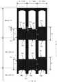
图2为本发明实施例一种第一基板的等效电路图。如图2所示,第一基板1包括M条栅线4、M条公共电极线5和N对数据线,每对数据线包括第一数据线6和第二数据线7,沿水平方向延伸且平行设置的多条栅线4和多条公共电极线5限定出M个显示行,沿竖直方向延伸且平行设置的多条第一数据线6和多条第二数据线7限定出N个显示列,因而M条栅线4、M条公共电极线5、N条第一数据线6和N条第二数据线7垂直交叉限定出呈阵列排布的M*N个子像素,M和N为大于或等于1的正整数。每个子像素包括薄膜晶体管3、像素电极8和公共电极9,薄膜晶体管3的源电极与第一数据线6或第二数据线7连接,薄膜晶体管3的漏电极与所在子像素的像素电极8连接,公共电极9与公共电极线5连接。在一显示行中,栅线4设置在邻近下一显示行的一侧,公共电极线5设置在邻近上一显示行的一侧,即栅线4设置在本显示行子像素的下侧,公共电极线5设置在本显示行子像素的上侧。在一显示列中,第一数据线6设置在邻近上一显示列的一侧,第二数据线7设置在邻近下一显示列的一侧,即第一数据线6设置在本显示列子像素的左侧,位于本显示列与左侧显示列之间,第二数据线7设置在本显示列子像素的右侧,位于本显示列与右侧显示列之间。M个显示行中,包括M/2个奇数显示行和M/2个偶数显示行。M/2个奇数显示行中子像素的薄膜晶体管3与第一数据线6连接,M/2个偶数显示行中子像素的薄膜晶体管3与第二数据线7连接。FIG. 2 is an equivalent circuit diagram of a first substrate according to an embodiment of the present invention. As shown in Figure 2, the first substrate 1 includes
在示例性实施方式中,第二基板2包括阵列排布的M*N个滤光单元22,M*N个滤光单元22与M*N个子像素的位置一一对应,相邻的两个滤光单元22之间设置有黑矩阵21。In an exemplary embodiment, the
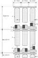
图3是本发明实施例一种显示面板的俯视图,示意了显示面板中2个显示行和3个显示列的黑矩阵21和滤光单元22。在示例性实施方式中,2个显示行分别为第k显示行和第k+1显示行,第k显示行和第k+2显示行为奇数显示行,第k+1显示行为偶数显示行。FIG. 3 is a top view of a display panel according to an embodiment of the present invention, illustrating a
在示例性实施方式中,第一基板1的每个显示行中,包括沿显示行方向周期性排布的第一子像素、第二子像素和第三子像素,第二基板2的每个显示行中,包括沿显示行方向周期性排布的第一滤光单元、第二滤光单元和第三滤光单元,第一滤光单元的位置与第一子像素的位置相对应,第二滤光单元的位置与第二子像素的位置相对应,第三滤光单元的位置与第三子像素相对应。由于第二基板2的滤光单元与第一基板1的子像素一一对应,因此本公开的后续描述中,将第一基板1的子像素和第二基板2的滤光单元统一采用子像素来说明。In an exemplary embodiment, each display row of the first substrate 1 includes first sub-pixels, second sub-pixels and third sub-pixels periodically arranged along the direction of the display row, each of the
在示例性实施方式中,第二基板2中,黑矩阵21位于相邻的两个子像素(滤光单元)之间,黑矩阵21包括位于相邻显示行的子像素之间的遮挡行211和位于相邻显示列的子像素之间的遮挡列212,遮挡行211被配置为遮挡第一基板1的栅线、公共电极线和薄膜晶体管,遮挡列212被配置为遮挡第一基板1的第一数据线和第二数据线。In an exemplary embodiment, in the
在示例性实施方式中,在数据线的延伸方向Y,位于第k显示行的子像素与第k+1显示行的子像素之间的遮挡行211具有第一宽度,位于第k+1显示行的子像素与第k+2显示行的子像素之间的遮挡行211具有第二宽度,第一宽度不等于第二宽度。所述第k显示行和第k+2显示行中子像素的薄膜晶体管与所述第一数据线连接,所述第k+1显示行中子像素的薄膜晶体管与所述第二数据线连接。也即是说,如果k为奇数,设置第k(奇数)显示行与第k+1(偶数)显示行之间的遮挡行具有第一宽度,第k+1(偶数)显示行与第k+2(奇数)显示行之间的遮挡行具有第二宽度,第一宽度不等于第二宽度。或者,如果k为偶数,设置第k(偶数)显示行与第k+1(奇数)显示行之间的遮挡行具有第一宽度,第k+1(奇数)显示行与第k+2(偶数)显示行之间的遮挡行具有第二宽度,第一宽度不等于第二宽度。本公开中,数据线的延伸方向Y是指平行于数据线的方向。In an exemplary embodiment, in the extending direction Y of the data lines, the shielding
在示例性实施方式中,位于第k显示行的子像素与第k+1显示行的子像素之间的遮挡行211包括位于第k显示行内的上边缘和位于第k+1显示行内的下边缘。位于第k显示行内的上边缘包括位于第k显示行的第一子像素内的第一上边缘101、位于第k显示行的第二子像素内的第二上边缘201和位于第k显示行的第三子像素内的第三上边缘301。位于第k+1显示行内的下边缘包括位于第k+1显示行的第一子像素内的第一下边缘102、位于第k+1显示行的第二子像素内的第二下边缘202和位于第k+1显示行的第三子像素内的第三下边缘302。在数据线的延伸方向Y,第一上边缘101与第一下边缘102之间的距离为第一距离L1,第二上边缘201与第二下边缘202之间的距离为第二距离L2,第三上边缘301与第三下边缘302之间的距离为第三距离L3。In an exemplary embodiment, the shielding
在示例性实施方式中,位于第k+1显示行的子像素与第k+2显示行的子像素之间的遮挡行211包括位于第k+1显示行内的上边缘和位于第k+2显示行内的下边缘。位于第k+1显示行内的上边缘包括位于第k+1显示行的第一子像素内的第四上边缘401、位于第k+1显示行的第二子像素内的第五上边缘501和位于第k+1显示行的第三子像素内的第六上边缘601。位于第k+2显示行内的下边缘包括位于第k+2显示行的第一子像素内的第四下边缘402、位于第k+2显示行的第二子像素内的第五下边缘502和位于第k+2显示行的第三子像素内的第六下边缘602。在数据线的延伸方向Y,第四上边缘401与第四下边缘402之间的距离为第四距离L4,第五上边缘501与第五下边缘502之间的距离为第五距离L5,第六上边缘601与第六下边缘602之间的距离为第六距离L6。In an exemplary embodiment, the
在示例性实施方式中,第一宽度不等于第二宽度包括如下任意一种或多种:第一距离L1小于第四距离L4,第二距离L2小于第五距离L5,第三距离L3大于第六距离L6。In an exemplary embodiment, the first width not equal to the second width includes any one or more of the following: the first distance L1 is smaller than the fourth distance L4, the second distance L2 is smaller than the fifth distance L5, and the third distance L3 is larger than the fifth distance L5. Six distance from L6.
在示例性实施方式中,第一距离L1与第四距离L4之差约为10μm~20μm,第二距离L2与第五距离L5之差约为10μm~20μm,第三距离L3与第六距离L6之差约为1μm~5μm。在一些可能的实现方式中,第一距离L1与第四距离L4之差约为13μm~15μm,第二距离L2与第五距离L5之差约为13μm~15μm,第三距离L3与第六距离L6之差约为2.5μm~3.5μm。In an exemplary embodiment, the difference between the first distance L1 and the fourth distance L4 is about 10 μm-20 μm, the difference between the second distance L2 and the fifth distance L5 is about 10 μm-20 μm, and the third distance L3 and the sixth distance L6 The difference is about 1 μm to 5 μm. In some possible implementations, the difference between the first distance L1 and the fourth distance L4 is about 13 μm to 15 μm, the difference between the second distance L2 and the fifth distance L5 is about 13 μm to 15 μm, and the third distance L3 and the sixth distance The difference between L6 is about 2.5 μm to 3.5 μm.
在示例性实施方式中,第三距离L3大于第一距离L1,第三距离L3大于第二距离L2,第一距离L1等于第二距离L2。In an exemplary embodiment, the third distance L3 is greater than the first distance L1, the third distance L3 is greater than the second distance L2, and the first distance L1 is equal to the second distance L2.
在一些可能的实现方式中,第三距离L3与第一距离L1之差约为10μm~35μm,第三距离L3与第二距离L2之差约为10μm~35μm。In some possible implementation manners, the difference between the third distance L3 and the first distance L1 is about 10 μm˜35 μm, and the difference between the third distance L3 and the second distance L2 is about 10 μm˜35 μm.
在示例性实施方式中,第六距离L6大于第四距离L4,第六距离L6大于第五距离L5,第四距离L4等于第五距离L5。In an exemplary embodiment, the sixth distance L6 is greater than the fourth distance L4, the sixth distance L6 is greater than the fifth distance L5, and the fourth distance L4 is equal to the fifth distance L5.
在一些可能的实现方式中,第六距离L6与第四距离L4之差约为10μm~20μm,第六距离L6与第五距离L5之差约为10μm~20μm。In some possible implementation manners, the difference between the sixth distance L6 and the fourth distance L4 is about 10 μm˜20 μm, and the difference between the sixth distance L6 and the fifth distance L5 is about 10 μm˜20 μm.
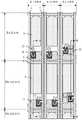
在示例性实施方式中,位于第k显示行的第一子像素内的遮挡行设置有第一凸起103,位于第k显示行的第二子像素内的遮挡行设置有第二凸起203。第一凸起103设置在第一上边缘101上,向着远离第一下边缘102的方向延伸,第二凸起203设置在第二上边缘201上,向着远离第二下边缘202的方向延伸。In an exemplary embodiment, the shading row located in the first sub-pixel of the kth display row is provided with a
在示例性实施方式中,在栅线的延伸方向X,第一凸起103位于第一子像素中设置薄膜晶体管的一侧,第二凸起203位于第二子像素中设置薄膜晶体管的一侧。由于第k显示行为奇数显示行,第k显示行中子像素的薄膜晶体管与位于子像素左侧的第一数据线连接,因而第k显示行中子像素的薄膜晶体管位于子像素的左侧,第一凸起103位于第一子像素的左侧,第二凸起203位于第二子像素的左侧。本公开中,栅线的延伸方向X是指平行于栅线的方向。In an exemplary embodiment, in the extending direction X of the gate line, the
在示例性实施方式中,在平行于显示面板的平面内,第一凸起103和第二凸起203的形状可以包括矩形或梯形。In an exemplary embodiment, in a plane parallel to the display panel, the shape of the
在示例性实施方式中,第一凸起103和第二凸起203的形状为矩形或梯形,第一凸起103包括第一凸起上边缘,第二凸起203包括第二凸起上边缘,在数据线的延伸方向Y,第一凸起上边缘与第一上边缘101之间的距离L7约为10μm~20μm,第二凸起上边缘与第二上边缘201之间的距离L8约为10μm~20μm。In an exemplary embodiment, the
在示例性实施方式中,在数据线的延伸方向Y,第三上边缘301与第一上边缘101之间的距离大于第一凸起上边缘与第一上边缘101之间的距离L7,第三上边缘301与第二上边缘201之间的距离大于第二凸起上边缘与第二上边缘201之间的距离L8。In an exemplary embodiment, in the extending direction Y of the data line, the distance between the third
在示例性实施方式中,所述第一下边缘、第二下边缘和第三下边缘均为沿所述栅线的延伸方向延伸的平直边缘;所述第四上边缘、第五上边缘和第六上边缘均为沿所述栅线的延伸方向延伸的平直边缘;所述第四下边缘、第五下边缘和第六下边缘上均设置有凸块,所述凸块分别设置在所述第四下边缘、第五下边缘和第六下边缘邻近两侧遮挡列的位置。In an exemplary embodiment, the first lower edge, the second lower edge and the third lower edge are straight edges extending along the extending direction of the grid lines; the fourth upper edge and the fifth upper edge and the sixth upper edge are straight edges extending along the extending direction of the grid lines; the fourth lower edge, the fifth lower edge and the sixth lower edge are all provided with bumps, and the bumps are respectively arranged The fourth lower edge, the fifth lower edge and the sixth lower edge are adjacent to the positions of the blocking columns on both sides.
在示例性实施方式中,所述凸块包括直角三角形,所述直角三角形的第一直边分别设置在所述第四下边缘、第五下边缘和第六下边缘上,所述直角三角形的第二直边分别设置在所述第四下边缘、第五下边缘和第六下边缘两侧的遮挡列上。In an exemplary embodiment, the bump includes a right triangle, the first straight sides of the right triangle are respectively arranged on the fourth lower edge, the fifth lower edge and the sixth lower edge, and the first straight sides of the right triangle The second straight sides are respectively arranged on the shielding rows on both sides of the fourth lower edge, the fifth lower edge and the sixth lower edge.
在示例性实施方式中,所述第一基板包括叠设的第一导电层、第一金属层、第一绝缘层、半导体层、第二金属层、第二绝缘层和第二导电层;所述第一导电层包括设置在每个子像素内的公共电极;所述第一金属层包括栅线和公共电极线、设置在每个子像素内的栅电极和设置在所述第三子像素内的第一连接电极,所述栅线与每个子像素内的栅电极连接,所述公共电极线与每个子像素内的公共电极连接,所述第一连接电极与所述第三子像素的公共电极连接;所述半导体层包括设置在每个子像素内的有源层;所述第二金属层包括第一数据线、第二数据线以及设置在每个子像素内的源电极和漏电极,第k显示行中,每个子像素的源电极与所述第一数据线连接,第k+1显示行中,每个子像素的源电极与所述第二数据线连接,所述源电极与漏电极之间形成导电沟道;所述第二导电层包括设置在每个子像素内的像素电极和设置在所述第三子像素中的第二连接电极,所述像素电极通过过孔与所在子像素的漏电极连接,所述第二连接电极通过过孔分别与第一连接电极和公共电极线连接。In an exemplary embodiment, the first substrate includes a stacked first conductive layer, a first metal layer, a first insulating layer, a semiconductor layer, a second metal layer, a second insulating layer, and a second conductive layer; The first conductive layer includes a common electrode arranged in each sub-pixel; the first metal layer includes a gate line and a common electrode line, a gate electrode arranged in each sub-pixel, and a gate electrode arranged in the third sub-pixel The first connection electrode, the gate line is connected to the gate electrode in each sub-pixel, the common electrode line is connected to the common electrode in each sub-pixel, the first connection electrode is connected to the common electrode of the third sub-pixel connection; the semiconductor layer includes an active layer arranged in each sub-pixel; the second metal layer includes a first data line, a second data line, and a source electrode and a drain electrode arranged in each sub-pixel, the kth In the display row, the source electrode of each sub-pixel is connected to the first data line, in the k+1th display row, the source electrode of each sub-pixel is connected to the second data line, and the source electrode and the drain electrode are A conductive channel is formed between them; the second conductive layer includes a pixel electrode arranged in each sub-pixel and a second connection electrode arranged in the third sub-pixel, and the pixel electrode is connected to the corresponding sub-pixel through a via hole. The drain electrode is connected, and the second connection electrode is respectively connected to the first connection electrode and the common electrode line through via holes.
在示例性实施方式中,第k显示行中,所述第一子像素、第二子像素和第三子像素中的公共电极设置有第一公共电极凸起,每个子像素的第一公共电极凸位于所述公共电极邻近第k-1显示行的一侧;所述第三子像素中的公共电极设置有第二公共电极凸起,所述第二公共电极凸起位于所述公共电极邻近下一显示行的一侧,所述第一连接电极设置在所述第二公共电极凸起上。In an exemplary embodiment, in the kth display row, the common electrodes in the first subpixel, the second subpixel, and the third subpixel are provided with a first common electrode protrusion, and the first common electrode of each subpixel The protrusion is located on the side of the common electrode adjacent to the k-1th display row; the common electrode in the third sub-pixel is provided with a second common electrode protrusion, and the second common electrode protrusion is located adjacent to the common electrode On one side of the next display row, the first connection electrode is disposed on the second common electrode protrusion.
在示例性实施方式中,在相邻公共电极线之间的第一间隔区域,所述公共电极线具有第三宽度,在相邻第一间隔区域之间的第二间隔区域,所述公共电极线具有第四宽度,所述第三宽度小于所述第四宽度;在所述第一间隔区域,所述栅线具有第五宽度,在所述第二间隔区域,所述栅线具有第六宽度,所述第五宽度小于所述第六宽度。In an exemplary embodiment, in a first spaced area between adjacent common electrode lines, the common electrode line has a third width, and in a second spaced area between adjacent first spaced areas, the common electrode line The line has a fourth width, and the third width is smaller than the fourth width; in the first interval region, the gate line has a fifth width, and in the second interval region, the gate line has a sixth width. width, the fifth width is smaller than the sixth width.
在示例性实施方式中,所述第一子像素、第二子像素和第三子像素中的栅电极均为矩形状,所述第一子像素和第二子像素中栅电极的长边沿着显示行方向延伸,所述第三子像素中的栅电极的长边沿着显示列方向延伸。In an exemplary embodiment, the gate electrodes in the first sub-pixel, the second sub-pixel and the third sub-pixel are all rectangular, and the long sides of the gate electrodes in the first sub-pixel and the second sub-pixel are along the The display row direction extends, and the long side of the gate electrode in the third sub-pixel extends along the display column direction.
在示例性实施方式中,所述第二连接电极的一端通过所述第一绝缘层和第二绝缘层上开设的过孔与所述第一连接电极连接,第二连接电极的另一端通过所述第一绝缘层和第二绝缘层上开设的过孔与下一显示行的公共电极线连接。In an exemplary embodiment, one end of the second connecting electrode is connected to the first connecting electrode through a via hole opened on the first insulating layer and the second insulating layer, and the other end of the second connecting electrode is connected to the first connecting electrode through the via hole. The via holes opened on the first insulating layer and the second insulating layer are connected to the common electrode lines of the next display row.
在示例性实施方式中,每个子像素中,所述像素电极与漏电极的连接区域与所述黑矩阵存在交叠,所述像素电极的边缘区域与黑矩阵存在交叠。In an exemplary embodiment, in each sub-pixel, the connection area between the pixel electrode and the drain electrode overlaps with the black matrix, and the edge area of the pixel electrode overlaps with the black matrix.
在示例性实施方式中,第一子像素(第一滤光单元)为红色子像素(红色滤光单元),第二子像素(第二滤光单元)为绿色子像素(绿色滤光单元),第三子像素(第三滤光单元)为蓝色子像素(蓝色滤光单元)。In an exemplary embodiment, the first sub-pixel (first filter unit) is a red sub-pixel (red filter unit), and the second sub-pixel (second filter unit) is a green sub-pixel (green filter unit) , the third sub-pixel (third filter unit) is a blue sub-pixel (blue filter unit).
下面通过显示面板的制备过程的示例说明显示面板的结构。本公开所说的“构图工艺”包括沉积膜层、涂覆光刻胶、掩模曝光、显影、刻蚀和剥离光刻胶处理。沉积可以采用溅射、蒸镀和化学气相沉积中的任意一种或多种,涂覆可以采用喷涂和旋涂中的任意一种或多种,刻蚀可以采用干刻和湿刻中的任意一种或多种。“薄膜”是指将某一种材料在基底上利用沉积或涂覆工艺制作出的一层薄膜。若在整个制作过程中该“薄膜”无需构图工艺,则该“薄膜”还可以称为“层”。若在整个制作过程中该“薄膜”需构图工艺,则在构图工艺前称为“薄膜”,构图工艺后称为“层”。经过构图工艺后的“层”中包含至少一个“图案”。本公开中所说的“A和B同层设置”是指,A和B通过同一次构图工艺同时形成。本公开示例性实施例中,“A的正投影包含B的正投影”是指,B的正投影的边界落入A的正投影的边界范围内,或者A的正投影的边界与B的正投影的边界完全重叠。The structure of the display panel will be described below through an example of the manufacturing process of the display panel. The “patterning process” mentioned in this disclosure includes deposition of film layer, coating of photoresist, mask exposure, development, etching and stripping of photoresist. Any one or more of sputtering, evaporation and chemical vapor deposition can be used for deposition, any one or more of spray coating and spin coating can be used for coating, and any of dry etching and wet etching can be used for etching. one or more. "Film" refers to a layer of film produced by depositing or coating a certain material on a substrate. If the "thin film" does not require a patterning process during the entire manufacturing process, the "thin film" can also be called a "layer". If the "film" requires a patterning process during the entire production process, it is called a "film" before the patterning process, and it is called a "layer" after the patterning process. The "layer" after the patterning process contains at least one "pattern". "A and B are arranged in the same layer" in this disclosure means that A and B are formed simultaneously through the same patterning process. In an exemplary embodiment of the present disclosure, "the orthographic projection of A includes the orthographic projection of B" means that the boundary of the orthographic projection of B falls within the boundary range of the orthographic projection of A, or the boundary of the orthographic projection of A is in the same range as the orthographic projection of B. The projected boundaries completely overlap.
本发明实施例显示面板的制备过程主要包括两部分,第一部分包括基板制备,第二部分包括对位压合(对盒)。其中,基板制备包括第一基板制备和第二基板制备,两者没有先后次序要求,可以同时进行。在示例性实施方式中,本发明实施例的第一基板可以是阵列基板,第二基板可以是彩膜基板。下面分别说明两部分的处理过程。The manufacturing process of the display panel according to the embodiment of the present invention mainly includes two parts, the first part includes substrate preparation, and the second part includes alignment pressing (box alignment). Wherein, the preparation of the substrate includes the preparation of the first substrate and the preparation of the second substrate, and there is no order requirement for the two, and they can be carried out at the same time. In an exemplary embodiment, the first substrate of the embodiment of the present invention may be an array substrate, and the second substrate may be a color filter substrate. The processing procedures of the two parts are described below.
一、第一部分中阵列基板的制备1. Preparation of the array substrate in the first part
图4A~图9C示意了阵列基板的制备过程,阵列基板示意了2个显示行、三个显示列中6个子像素的结构。在示例性实施方式中,第k显示行和第k+2显示行可以为奇数行,第k+1显示行可以为偶数行。每个显示行中可以包括第一子像素、第二子像素和第三子像素,分别对应于彩膜基板的第一滤光单元、第二滤光单元和第三滤光单元。4A to 9C illustrate the preparation process of the array substrate, and the array substrate illustrates the structure of 6 sub-pixels in 2 display rows and 3 display columns. In an exemplary embodiment, the kth display row and the k+2th display row may be odd-numbered rows, and the k+1th display row may be even-numbered rows. Each display row may include a first sub-pixel, a second sub-pixel and a third sub-pixel, respectively corresponding to the first filter unit, the second filter unit and the third filter unit of the color filter substrate.
(1)形成第一导电层图案。在示例性实施方式中,形成第一导电层图案可以包括:在第一基底上沉积第一透明导电薄膜,通过构图工艺对第一透明导电薄膜进行构图,在第一基底10上形成第一导电层图案,第一导电层图案至少包括设置在每个子像素内的公共电极9,如图4A、图4B和图4C所示,图4B为图4A中A-A向的剖视图,图4C为图4A中B-B向的剖视图。(1) Forming a first conductive layer pattern. In an exemplary embodiment, forming the first conductive layer pattern may include: depositing a first transparent conductive film on the first substrate, patterning the first transparent conductive film through a patterning process, and forming a first conductive layer on the
在示例性实施方式中,在每个显示行中,公共电极9为板状电极,第一子像素和第二子像素的公共电极9的形状和尺寸相同,第三子像素的公共电极9的形状和尺寸不同于第一子像素和第二子像素,第k显示行的第一子像素与第k+1显示行的第一子像素两者的公共电极9的形状和尺寸不同,第k显示行的第二子像素与第k+1显示行的第二子像素两者的公共电极9的形状和尺寸不同,第k显示行的第三子像素与第k+1显示行的第三子像素两者的公共电极9的形状和尺寸不同。In an exemplary embodiment, in each display row, the
在示例性实施方式中,第k显示行的第一子像素、第二子像素和第三子像素中的公共电极9设置有第一公共电极凸起,每个子像素的第一公共电极凸位于公共电极9邻近第k-1显示行的一侧,每个子像素的第一公共电极凸位被配置为与后续形成的公共电极线连接,实现显示行方向每个子像素的公共电极9的相互连接。In an exemplary embodiment, the
在示例性实施方式中,第k显示行的第三子像素和第k+1显示行的第三子像素中的公共电极9设置有第二公共电极凸起,第k显示行的第三子像素的第二公共电极凸起位于公共电极9邻近第k+1显示行的一侧,第k+1显示行的第三子像素的第二公共电极凸起位于公共电极9邻近第k+2显示行的一侧,第二公共电极凸起被配置为通过后续形成的第一连接电极和第二连接电极,使第k显示行的第三子像素中的公共电极9与第k+1显示行的第三子像素中的公共电极9连接,实现显示列方向第三子像素的公共电极9的相互连接。由于显示行方向各个子像素中的公共电极9通过公共电极线5相互连接,显示列方向各个第三子像素的通过第二公共电极凸起、第一连接电极、第二连接电极和公共电极线5相互连接,因而实现了所有子像素的公共电极9相互连接,使得所有子像素的公共电极9具有相同的电位,提高显示面板的显示效果。In an exemplary embodiment, the
在示例性实施方式中,第k显示行中,公共电极线5在基底10上的正投影中的部分区域与公共电极9在基底10上的正投影的部分区域存在交叠。也就是说,公共电极线5的一部分设置在公共电极9上,另一部分设置在基底10上。第k+1显示行中,公共电极线5在基底10上的正投影中的全部区域与公共电极9在基底10上的正投影的部分区域存在交叠。也就是说,公共电极线5设置在公共电极9上。In an exemplary embodiment, in the kth display row, a partial area of the orthographic projection of the
(2)形成第一金属层图案。在示例性实施方式中,形成第一金属层图案可以包括:在形成有前述图案的第一基底上沉积第一金属薄膜,通过构图工艺对第一金属薄膜进行构图,在第一基底10上形成第一金属图案,第一金属图案至少包括沿水平方向延伸的栅线4和公共电极线5、设置在每个子像素内的栅电极11、设置在第三子像素内的第一连接电极31,如图5A、图5B和图5C所示,图5B为图5A中A-A向的剖视图,图5C为图5A中B-B向的剖视图。(2) Forming the first metal layer pattern. In an exemplary embodiment, forming the first metal layer pattern may include: depositing a first metal thin film on the first substrate formed with the aforementioned pattern, patterning the first metal thin film through a patterning process, and forming on the
在示例性实施方式中,每个显示行的栅线4设置在本显示行的下侧,与本显示行中每个子像素的公共电极9间隔一定距离,与栅线4平行的公共电极线5设置在本显示行的上侧,搭设在本显示行中每个子像素的公共电极9上,实现显示行方向公共电极线5与每个子像素的公共电极9的连接。每个子像素中,栅电极11是与栅线4连接的一体结构。位于第三子像素内的第一连接电极31设置在第三子像素中公共电极9的第二公共电极凸起上,实现第一连接电极31与第三子像素的公共电极9的连接。第k显示行中,第一连接电极31设置在第三子像素的栅电极11的右侧,第k+1显示行中,第一连接电极31设置在第三子像素的栅电极11的左侧。In an exemplary embodiment, the
在示例性实施方式中,水平方向设置的公共电极线5可以为非等宽度设置。在相邻公共电极线5之间的第一间隔区域,公共电极线5具有第三宽度,在相邻第一间隔区域之间的第二间隔区域,公共电极线5具有第四宽度,第三宽度小于第四宽度。在第二间隔区域,由于公共电极线5与公共电极9连接,较宽的公共电极线5可以保证公共电极线5与公共电极9的可靠连接。由于后续工艺中,相邻公共电极线5之间的第一间隔区域设置有数据线,较窄的公共电极线5可以使得公共电极线5与后续形成的数据线具有较小的交叠面积,相当于公共电极线5在与数据线的交叠区域进行了减宽设计,因而可以减小公共电极线5与数据线之间的寄生电容,提高显示面板的电学性能。本公开中,公共电极线的宽度,是指在垂直于公共电极线方向公共电极线的尺寸。In an exemplary embodiment, the
在示例性实施方式中,水平方向设置的栅线4可以为非等宽度设置。相邻公共电极线5之间的第一间隔区域,栅线4具有第五宽度,在相邻第一间隔区域之间的第二间隔区域,栅线4具有第六宽度,第五宽度小于第六宽度。在第二间隔区域,由于栅线4连接栅电极11,较宽的栅线4可以增加栅电极11的面积,提高薄膜晶体管的电学性能。由于后续工艺中,相邻公共电极线5之间的第一间隔区域设置有数据线,较窄的栅线4可以使得栅线4与后续形成的数据线具有较小的交叠面积,相当于栅线4在与数据线的交叠区域进行了减宽设计,因而可以减小栅线4与数据线之间的寄生电容,提高显示面板的电学性能。本公开中,栅线的宽度,是指在垂直于栅线方向栅线的尺寸。In an exemplary embodiment, the
在示例性实施方式中,第一子像素、第二子像素和第三子像素中的栅电极11均为矩形状,第一子像素和第二子像素中栅电极11的长边沿着显示行方向延伸,第三子像素中的栅电极11的长边沿着显示列方向延伸。在垂直于栅线方向,第三子像素中栅电极11的上边缘与栅线4之间的距离大于第一子像素和第二子像素中栅电极11的上边缘与栅线4之间的距离。在平行于栅线方向,第三子像素中栅电极11两个边缘之间的距离小于第一子像素和第二子像素中栅电极11两个边缘之间的距离。由于第三子像素中的公共电极9设置有向着栅线4延伸的第二公共电极凸起,因而第三子像素中的栅电极11设计成向着公共电极9延伸的矩形形状,以保证第三子像素中栅电极11的面积。In an exemplary embodiment, the
(3)形成半导体层图案。在示例性实施方式中,形成半导体层图案可以包括:在形成有前述图案的第一基底上依次沉积第一绝缘薄膜和半导体层薄膜,通过构图工艺对半导体层薄膜进行构图,形成覆盖第一金属层图案和第一导电层图案的第一绝缘层12,以及设置在第一绝缘层12上的半导体层图案,半导体层图案至少包括设置在每个子像素内的有源层13,每个有源层13的位置与所在子像素内栅电极11的位置相对应,如图6A、图6B和图6C所示,图6B为图6A中A-A向的剖视图,图6C为图6A中B-B向的剖视图。(3) Forming a semiconductor layer pattern. In an exemplary embodiment, forming the semiconductor layer pattern may include: sequentially depositing a first insulating film and a semiconductor layer film on the first substrate formed with the aforementioned pattern, and patterning the semiconductor layer film through a patterning process to form a layer covering the first metal layer. The layer pattern and the first insulating
在示例性实施方式中,每个子像素内的有源层13的形状可以相同,第k显示行中每个子像素内有源层13的位置不同于第k+1显示行中每个子像素内有源层13的位置。In an exemplary embodiment, the shape of the
在示例性实施方式中,由于第k显示行为奇数行,第一子像素、第二子像素和第三子像素中的薄膜晶体管与位于子像素左侧的第一数据线连接,因此第k显示行中的有源层13位于靠近第一数据线的一侧(左侧),可以简化薄膜晶体管中源电极的结构,减小源电极与栅电极之间的寄生电容,提高薄膜晶体管的电学性能。由于第k+1显示行为偶数行,第一子像素、第二子像素和第三子像素中的薄膜晶体管与位于子像素右侧的第二数据线连接,因此第k+1显示行中的有源层13位于靠近第二数据线的一侧(右侧),可以简化薄膜晶体管中源电极的结构,减小源电极与栅电极之间的寄生电容,提高薄膜晶体管的电学性能。In an exemplary embodiment, since the kth display row is an odd row, the thin film transistors in the first subpixel, the second subpixel, and the third subpixel are connected to the first data line on the left side of the subpixel, so the kth display The
(4)形成第二金属层图案。在示例性实施方式中,形成第一金属层图案可以包括:在形成有前述图案的第一基底上沉积第二金属薄膜,通过构图工艺对第二金属薄膜进行构图,形成设置在第一绝缘层12上的第二金属图案,第二金属图案至少包括沿竖直方向延伸的第一数据线6和第二数据线7、设置在每个子像素内的源电极14和漏电极15,如图7A、图7B和图7C所示,图7B为图7A中A-A向的剖视图,图7C为图7A中B-B向的剖视图。(4) Forming a second metal layer pattern. In an exemplary embodiment, forming the first metal layer pattern may include: depositing a second metal thin film on the first substrate formed with the aforementioned pattern, patterning the second metal thin film through a patterning process, and forming a layer disposed on the first insulating layer. 12, the second metal pattern at least includes a
在示例性实施方式中,每个显示列中的第一数据线6和第二数据线7形成双数据线,第一数据线6设置在每个显示列的左侧,用于向第k显示行(奇数行)的子像素提供数据信号,第二数据线7设置在每个显示列的右侧,用于向第k+1显示行(偶数行)的子像素提供数据信号。第k显示行中,每个子像素的源电极14是与第一数据线6连接的一体结构,第k+1显示行中,每个子像素的源电极14是与第二数据线7连接的一体结构。每个子像素中,源电极14的一端和漏电极15的一端分别设置在有源层13上,源电极14与漏电极15之间形成导电沟道。In an exemplary embodiment, the
在示例性实施方式中,在每个显示行中,第一子像素和第二子像素的源电极14和漏电极15的形状、尺寸和位置相同,第三子像素与第一子像素和第二子像素的源电极14和漏电极15的形状、尺寸和位置不同。第k显示行的第一子像素与第k+1显示行的第一子像素两者的源电极14和漏电极15的形状和尺寸相同,位置相对于竖直中心线镜像对称。第k显示行的第二子像素与第k+1显示行的第二子像素两者的源电极14和漏电极15的形状和尺寸相同,位置相对于竖直中心线镜像对称。第k显示行的第三子像素与第k+1显示行的第三子像素两者的源电极14和漏电极15的形状和尺寸相同,位置相对于竖直中心线镜像对称。竖直中心线是每个显示列中第一数据线6和第二数据线7的中心线。In an exemplary embodiment, in each display row, the shape, size and position of the
在一些可能的实现方式中,形成半导体层图案和形成第二金属层图案可以采用一次构图工艺,先依次沉积第一绝缘薄膜、半导体层薄膜和第二金属薄膜,在第二金属薄膜上涂覆一层光刻胶,采用半色调或灰色调掩膜板对光刻胶进行曝光显影,然后通过二次刻蚀工艺和一次灰化工艺,形成有源层、第一数据线、第二数据线、源电极和漏电极图案,第一数据线、第二数据线、源电极和漏电极图案下保留有半导体层薄膜。In some possible implementations, the formation of the semiconductor layer pattern and the formation of the second metal layer pattern can adopt a patterning process, first depositing the first insulating film, the semiconductor layer film and the second metal film in sequence, and coating on the second metal film A layer of photoresist, using half-tone or gray-tone mask to expose and develop the photoresist, and then through the second etching process and the first ashing process to form the active layer, the first data line, and the second data line , the source electrode and the drain electrode pattern, the semiconductor layer thin film remains under the first data line, the second data line, the source electrode and the drain electrode pattern.
(5)形成第二绝缘层图案。在示例性实施方式中,形成第二绝缘层图案可以包括:在形成有前述图案的第一基底上,沉积第二绝缘薄膜,通过构图工艺对第二绝缘薄膜进行构图,形成覆盖第二金属图案的第二绝缘层16图案,第二绝缘层16图案至少包括多个过孔,如图8A、图8B和图8C所示,图8B为图8A中A-A向的剖视图,图8C为图8A中B-B向的剖视图。(5) Forming a second insulating layer pattern. In an exemplary embodiment, forming the second insulating layer pattern may include: depositing a second insulating film on the first substrate formed with the aforementioned pattern, and patterning the second insulating film through a patterning process to form a covering second metal pattern The second insulating
在示例性实施方式中,过孔可以包括:设置在每个子像素中漏电极15所在位置的第一过孔K1、设置在第三子像素中的第一连接电极31所在位置的第二过孔K2和设置在第三子像素中公共电极线5所在位置的第三过孔K3,第一过孔K1内的第二绝缘层16被刻蚀掉,暴露出漏电极15的表面,第二过孔K2内的第二绝缘层16和第一绝缘层12被刻蚀掉,暴露出第一连接电极31的表面,第三过孔K3内的第二绝缘层16和第一绝缘层12被刻蚀掉,暴露出公共电极线5的表面。第k显示行的第三子像素中第三过孔K3的位置不同于第k+1显示行的第三子像素中第三过孔K3的位置。In an exemplary embodiment, the via hole may include: a first via hole K1 provided at the position of the
(6)形成第二导电层图案。在示例性实施方式中,形成第二导电层图案可以包括:在形成有前述图案的第一基底上沉积第二透明导电薄膜,通过构图工艺对第二透明导电薄膜进行构图,形成第二导电层图案,第二导电层图案至少包括设置在每个子像素内的像素电极8和设置在第三子像素中的第二连接电极32,如图9A、图9B和图9C所示,图9B为图9A中A-A向的剖视图,图9C为图9A中B-B向的剖视图。在示例性实施方式中,在每个子像素内,像素电极8为缝隙电极,通过第一过孔K1与所在子像素的漏电极15连接。在第三子像素内,第二连接电极32的一端通过第二过孔K2与第一连接电极31连接,另一端通过第三过孔K3与下一显示行的公共电极线5连接,实现显示列方向每个第三子像素中公共电极9的相互连接。在示例性实施方式中,在每个显示行中,第一子像素和第二子像素的像素电极8的形状和尺寸相同,第三子像素的像素电极8的形状和尺寸不同于第一子像素和第二子像素。第k显示行的第一子像素与第k+1显示行的第一子像素两者的像素电极8的形状和尺寸不同,第k显示行的第二子像素与第k+1显示行的第二子像素两者的像素电极8的形状和尺寸不同,第k显示行的第三子像素与第k+1显示行的第三子像素两者的像素电极8的形状和尺寸不同。在示例性实施方式中,由于显示列方向各个第三子像素的公共电极9通过第二公共电极凸起、第一连接电极31、第二连接电极32和公共电极线5相互连接,而显示行方向各个子像素中的公共电极9通过公共电极线5相互连接,因而实现了所有子像素的公共电极9相互连接,使得所有子像素的公共电极9具有相同的电位,提高显示面板的显示效果。(6) Forming a second conductive layer pattern. In an exemplary embodiment, forming the second conductive layer pattern may include: depositing a second transparent conductive film on the first substrate formed with the aforementioned pattern, and patterning the second transparent conductive film through a patterning process to form the second conductive layer. pattern, the second conductive layer pattern at least includes the
本发明实施例中,第一基底可以采用玻璃基底、石英基底或者塑料基底。第一金属薄膜和第二金属薄膜可以采用金属材料,采用磁控溅射方法(Sputter)沉积,如银(Ag)、铜(Cu)、铝(Al)、钛(Ti)和钼(Mo)中的任意一种或多种,或上述金属的合金材料,如铝钕合金(AlNd)或钼铌合金(MoNb),可以是单层结构,或者多层复合结构,如Ti/Al/Ti等。第一绝缘薄膜和第二绝缘薄膜可以采用硅氧化物SiOx、硅氮化物SiNx和氮氧化硅SiON中的任意一种或多种,可以是单层结构,或者多层复合结构,采用化学气相沉积(CVD)方式或等离子体增强化学气相沉积(PECVD)方式沉积。第一绝缘层称之为栅绝缘(GI)层,第二绝缘层也称之为钝化(PVX)层。第一透明导电薄膜和第二透明导电薄膜可以采用氧化铟锡ITO或氧化铟锌IZO。半导体层薄膜可以采用非晶态氧化铟镓锌材料(a-IGZO)、氮氧化锌(ZnON)、氧化铟锌锡(IZTO)、非晶硅(a-Si)、多晶硅(p-Si)、六噻吩或聚噻吩等材料,即本公开适用于基于氧化物(Oxide)技术、硅技术或有机物技术制造的晶体管。In the embodiment of the present invention, the first substrate may be a glass substrate, a quartz substrate or a plastic substrate. The first metal film and the second metal film can be metal materials, deposited by magnetron sputtering (Sputter), such as silver (Ag), copper (Cu), aluminum (Al), titanium (Ti) and molybdenum (Mo) Any one or more of them, or alloy materials of the above metals, such as aluminum neodymium alloy (AlNd) or molybdenum niobium alloy (MoNb), can be single-layer structure, or multi-layer composite structure, such as Ti/Al/Ti, etc. . The first insulating film and the second insulating film can use any one or more of silicon oxide SiOx, silicon nitride SiNx and silicon oxynitride SiON, and can be a single-layer structure or a multi-layer composite structure, using chemical vapor deposition (CVD) or plasma enhanced chemical vapor deposition (PECVD) deposition. The first insulating layer is called a gate insulating (GI) layer, and the second insulating layer is also called a passivation (PVX) layer. The first transparent conductive film and the second transparent conductive film can use indium tin oxide ITO or indium zinc oxide IZO. The semiconductor layer film can be made of amorphous indium gallium zinc oxide (a-IGZO), zinc oxynitride (ZnON), indium zinc tin oxide (IZTO), amorphous silicon (a-Si), polysilicon (p-Si), Materials such as hexathiophene or polythiophene, that is, the present disclosure is applicable to transistors manufactured based on oxide technology, silicon technology or organic technology.
这样,完成本发明实施例阵列基板的制备,每个子像素内的栅电极11、有源层13、源电极14和漏电极15构成薄膜晶体管,每个子像素内的公共电极9为板状电极,像素电压8为狭缝电极,公共电极9被配置为提供公共电压,像素电极8被配置为提供显示用像素电压,狭缝电极与板状电极之间产生的多维电场驱动液晶偏转。在显示行中,第一子像素、第二子像素和第三子像素中的公共电极9通过同一条公共电极线5相互连接,在显示列中,第k显示行中的公共电极9与第k+1显示行中的公共电极9通过第一连接电极31和第二连接电极32相互连接。In this way, the preparation of the array substrate of the embodiment of the present invention is completed, the
在一些可能的实现方式中,第一导电层图案可以包括像素电极,第二导电层图案可以包括公共电极,像素电极为板状电极,公共电极为狭缝电极。在一些可能的实现方式中,阵列基板的制备方法还可以包括形成平坦层、取向膜以及对取向膜进行配向等处理。In some possible implementation manners, the first conductive layer pattern may include a pixel electrode, the second conductive layer pattern may include a common electrode, the pixel electrode is a plate electrode, and the common electrode is a slit electrode. In some possible implementation manners, the method for preparing the array substrate may further include forming a flat layer, an alignment film, and aligning the alignment film.
二、第一部分中彩膜基板的制备2. Preparation of the color filter substrate in the first part
图10A~图11C示意了彩膜基板的制备过程,彩膜基板示意了2个显示行、三个显示列中6个滤光单元的结构。在示例性实施方式中,第k显示行可以为奇数行,第k+1显示行可以为偶数行。每个显示行中包括第一滤光单元、第二滤光单元和第三滤光单元,分别对应于阵列基板的第一子像素、第二子像素和第三子像素。在示例性实施方式中,第一滤光单元可以为红色滤光单元,第二滤光单元可以为绿色滤光单元,第三滤光单元可以为蓝色滤光单元。10A to 11C illustrate the manufacturing process of the color filter substrate, and the color filter substrate illustrates the structure of 6 filter units in 2 display rows and 3 display columns. In an exemplary embodiment, the k-th display line may be an odd-numbered line, and the k+1-th display line may be an even-numbered line. Each display row includes a first filter unit, a second filter unit and a third filter unit, respectively corresponding to the first sub-pixel, the second sub-pixel and the third sub-pixel of the array substrate. In an exemplary embodiment, the first filter unit may be a red filter unit, the second filter unit may be a green filter unit, and the third filter unit may be a blue filter unit.
(1)形成黑矩阵图案。在示例性实施方式中,形成黑矩阵图案可以包括:在第二基底20上涂覆黑矩阵薄膜,采用掩膜版对黑矩阵薄膜进行曝光,显影后在第二基底20上形成黑矩阵21图案,如图10A、图10B和图10C所示,图10B为图10A中C-C向的剖视图,图10C为图10A中D-D向的剖视图。(1) A black matrix pattern is formed. In an exemplary embodiment, forming a black matrix pattern may include: coating a black matrix film on the
在示例性实施方式中,彩膜基板上的黑矩阵21图案包括在栅线延伸方向X延伸的遮挡行211和在数据线延伸方向Y延伸遮挡列212,多个遮挡行211和遮挡列212相互交叉,形成多个开口区域,多个开口区域与阵列基板上的多个像素电极8的位置相对应。遮挡行211的位置与阵列基板上的栅线4、公共电压线5、薄膜晶体管的位置相对应,遮挡行211被配置为遮挡阵列基板上的栅线、公共电极线和薄膜晶体管,遮挡列212的位置与阵列基板上的第一数据线和第二数据线的位置相对应,遮挡列212被配置为遮挡阵列基板上的第一数据线和第二数据线。In an exemplary embodiment, the pattern of the
在示例性实施方式中,在竖直方向Y,位于第k显示行的滤光单元与第k+1显示行的滤光单元之间的遮挡行211具有第一宽度,位于第k+1显示行的滤光单元与第k+2显示行的滤光单元之间的遮挡行211具有第二宽度,第一宽度不等于第二宽度。本公开中,竖直方向Y是平行于数据线的方向。In an exemplary embodiment, in the vertical direction Y, the shielding
在示例性实施方式中,位于第k显示行的滤光单元与第k+1显示行的滤光单元之间的遮挡行211包括位于第k显示行内的上边缘和位于第k+1显示行内的下边缘。位于第k显示行内的上边缘包括位于第k显示行的第一滤光单元内的第一上边缘101、位于第k显示行的第二滤光单元内的第二上边缘201和位于第k显示行的第三滤光单元内的第三上边缘301。In an exemplary embodiment, the shielding
在示例性实施方式中,位于第k+1显示行内的下边缘包括位于第k+1显示行的第一滤光单元内的第一下边缘102、位于第k+1显示行的第二滤光单元内的第二下边缘202和位于第k+1显示行的第三滤光单元内的第三下边缘302。第一上边缘101与第一下边缘102之间的距离为第一距离L1,第二上边缘201与第二下边缘202之间的距离为第二距离L2,第三上边缘301与第三下边缘302之间的距离为第三距离L3。In an exemplary embodiment, the lower edge located in the k+1 display row includes the first
在示例性实施方式中,位于第k+1显示行的滤光单元与第k+2显示行的滤光单元之间的遮挡行211包括位于第k+1显示行内的上边缘和位于第k+2显示行内的下边缘。位于第k+1显示行内的上边缘包括位于第k+1显示行的第一滤光单元内的第四上边缘401、位于第k+1显示行的第二滤光单元内的第五上边缘501和位于第k+1显示行的第三滤光单元内的第六上边缘601。位于第k+2显示行内的下边缘包括位于第k+2显示行的第一滤光单元内的第四下边缘402、位于第k+2显示行的第二滤光单元内的第五下边缘502和位于第k+2显示行的第三滤光单元内的第六下边缘602。第四上边缘401与第四下边缘402之间的距离为第四距离L4,第五上边缘501与第五下边缘502之间的距离为第五距离L5,第六上边缘601与第六下边缘602之间的距离为第六距离L6。In an exemplary embodiment, the shielding
在示例性实施方式中,第一宽度不等于第二宽度包括如下任意一种或多种:第一距离L1小于第四距离L4,第二距离L2小于第五距离L5,第三距离L3大于第六距离L6。In an exemplary embodiment, the first width not equal to the second width includes any one or more of the following: the first distance L1 is smaller than the fourth distance L4, the second distance L2 is smaller than the fifth distance L5, and the third distance L3 is larger than the fifth distance L5. Six distance from L6.
在示例性实施方式中,第一距离L1与第四距离L4之差约为10μm~20μm,第二距离L2与第五距离L5之差约为10μm~20μm,第三距离L3与第六距离L6之差约为1μm~5μm。在一些可能的实现方式中,第一距离L1与第四距离L4之差约为13μm~15μm,第二距离L2与第五距离L5之差约为13μm~15μm,第三距离L3与第六距离L6之差约为2.5μm~3.5μm。In an exemplary embodiment, the difference between the first distance L1 and the fourth distance L4 is about 10 μm-20 μm, the difference between the second distance L2 and the fifth distance L5 is about 10 μm-20 μm, and the third distance L3 and the sixth distance L6 The difference is about 1 μm to 5 μm. In some possible implementations, the difference between the first distance L1 and the fourth distance L4 is about 13 μm to 15 μm, the difference between the second distance L2 and the fifth distance L5 is about 13 μm to 15 μm, and the third distance L3 and the sixth distance The difference between L6 is about 2.5 μm to 3.5 μm.
在示例性实施方式中,第三距离L3大于第一距离L1,第三距离L3大于第二距离L2,第一距离L1等于第二距离L2。In an exemplary embodiment, the third distance L3 is greater than the first distance L1, the third distance L3 is greater than the second distance L2, and the first distance L1 is equal to the second distance L2.
在一些可能的实现方式中,第三距离L3与第一距离L1之差约为10μm~35μm,第三距离L3与第二距离L2之差约为10μm~35μm。In some possible implementation manners, the difference between the third distance L3 and the first distance L1 is about 10 μm˜35 μm, and the difference between the third distance L3 and the second distance L2 is about 10 μm˜35 μm.
在示例性实施方式中,第六距离L6大于第四距离L4,第六距离L6大于第五距离L5,第四距离L4等于第五距离L5。In an exemplary embodiment, the sixth distance L6 is greater than the fourth distance L4, the sixth distance L6 is greater than the fifth distance L5, and the fourth distance L4 is equal to the fifth distance L5.
在一些可能的实现方式中,第六距离L6与第四距离L4之差约为10μm~20μm,第六距离L6与第五距离L5之差约为10μm~20μm。In some possible implementation manners, the difference between the sixth distance L6 and the fourth distance L4 is about 10 μm˜20 μm, and the difference between the sixth distance L6 and the fifth distance L5 is about 10 μm˜20 μm.
在示例性实施方式中,位于第k显示行的第一滤光单元内的遮挡行设置有第一凸起103,位于第k显示行的第二滤光单元内的遮挡行设置有第二凸起203。第一凸起103设置在第一上边缘101上,向着远离第一下边缘102的方向延伸,第二凸起203设置在第二上边缘201上,向着远离第二下边缘202的方向延伸。In an exemplary embodiment, the shielding row in the first filter unit of the kth display row is provided with a
在示例性实施方式中,在水平方向X,第一凸起103的位置与阵列基板上薄膜晶体管的位置相对应。本公开中,水平方向X是平行于栅线的方向。In an exemplary embodiment, in the horizontal direction X, the position of the
在示例性实施方式中,在平行于彩膜基板的平面内,第一凸起103和第二凸起203的形状可以包括矩形或梯形。In an exemplary embodiment, in a plane parallel to the color filter substrate, the shapes of the
在示例性实施方式中,第一凸起103包括第一凸起上边缘,第二凸起203包括第二凸起上边缘,在竖直方向Y,第一凸起上边缘与第一上边缘101之间的距离L7约为10μm~20μm,第二凸起上边缘与第二上边缘201之间的距离L8约为10μm~20μm。在水平方向X,第一凸起103和第二凸起203的宽度为所在滤光单元的宽度的1/3~1/2。In an exemplary embodiment, the
在示例性实施方式中,位于第k显示行的第一滤光单元与第k+1显示行的第一滤光单元之间的遮挡行包括设置有第一凸起103的第一上边缘101和平直的第一下边缘102,第一上边缘101和第一下边缘102沿水平方向X延伸。位于第k+1显示行的第一滤光单元与第k+2显示行的第一滤光单元之间的遮挡行包括平直的第四上边缘401和设置有两个凸块的第四下边缘402,两个凸块分别设置在第四下边缘402邻近两侧遮挡列的位置。在示例性实施方式中,凸块可以是直角三角形,两个直角三角形的第一直边分别设置在第四下边缘402上,两个直角三角形的第二直边分别设置在第四下边缘402两侧的遮挡列上。In an exemplary embodiment, the shielding row between the first filter unit of the kth display row and the first filter unit of the k+1th display row includes a first
在示例性实施方式中,位于第k显示行的第二滤光单元与第k+1显示行的第二滤光单元之间的遮挡行包括设置有第二凸起203的第二上边缘201和平直的第二下边缘202,第二上边缘201和平直的第二下边缘202沿水平方向X延伸。位于第k+1显示行的第二滤光单元与第k+2显示行的第二滤光单元之间的遮挡行包括平直的第五上边缘501和设置有两个凸块的第五下边缘502,两个凸块分别设置在第五下边缘502邻近两侧遮挡列的位置。在示例性实施方式中,凸块可以是直角三角形,两个直角三角形的第一直边分别设置在第五下边缘502上,两个直角三角形的第二直边分别设置在第五下边缘502两侧的遮挡列上。In an exemplary embodiment, the shielding row between the second filter unit of the kth display row and the second filter unit of the k+1th display row includes a second
在示例性实施方式中,位于第k显示行的第三滤光单元与第k+1显示行的第三滤光单元之间的遮挡行包括平直的第三上边缘301和平直的第三下边缘302,第三上边缘301和第三下边缘302沿水平方向X延伸。位于第k+1显示行的第三滤光单元与第k+2显示行的第三滤光单元之间的遮挡行包括平直的第六上边缘601和设置有两个凸块的第六下边缘602,两个凸块设置在第六下边缘602邻近两侧遮挡列的位置。在示例性实施方式中,凸块可以是直角三角形,两个直角三角形的第一直边分别设置在第六下边缘602上,两个直角三角形的第二直边分别设置在第六下边缘602两侧的遮挡列上。In an exemplary embodiment, the shielding row between the third filter unit of the kth display row and the third filter unit of the k+1th display row includes a straight third
在示例性实施方式中,在竖直方向Y,第三上边缘301与第一上边缘101之间的距离大于第一凸起上边缘与第一上边缘101之间的距离L7,第三上边缘301与第二上边缘201之间的距离大于第二凸起上边缘与第二上边缘201之间的距离L8。In an exemplary embodiment, in the vertical direction Y, the distance between the third
在示例性实施方式中,对于第k显示行与第k+1显示行之间的遮挡行,第一凸起103的上边缘与第一中心线的距离大于第一上边缘101与第一中心线的距离,第二凸起203的上边缘与第一中心线的距离大于第二上边缘201与第一中心线的距离,第三上边缘301与第一中心线的距离大于第一凸起103的上边缘与第一中心线的距离,第三上边缘301与第一中心线的距离大于第二凸起203的上边缘与第一中心线的距离。第三下边缘302与第一中心线的距离大于第一下边缘102与第一中心线的距离,第三下边缘302与第一中心线的距离大于第二下边缘202与第一中心线的距离。本公开中,第一中心线为位于第k显示行内的上边缘与位于第k+1显示行内的下边缘之间的水平方向X延伸的中线。In an exemplary embodiment, for the shaded row between the kth display row and the k+1th display row, the distance between the upper edge of the
在一些可能的实现方式中,第一凸起103的上边缘与第一中心线的距离等于第二凸起203的上边缘与第一中心线的距离,第一上边缘101与第一中心线的距离等于第二上边缘201与第一中心线的距离,第一下边缘102与第一中心线的距离等于第二下边缘202与第一中心线的距离。In some possible implementations, the distance between the upper edge of the
在示例性实施方式中,对于第k+1显示行与第k+2显示行之间的遮挡行,第六上边缘601与第二中心线的距离大于第四上边缘401与第二中心线的距离,第六上边缘601与第二中心线的距离大于第五上边缘501与第二中心线的距离,第六下边缘602与第二中心线的距离等于第四下边缘402与第二中心线的距离,第六下边缘602与第二中心线的距离等于第五下边缘502与第二中心线的距离。本公开中,第二中心线为位于第k+1显示行内的上边缘与位于第k+2显示行内的下边缘之间的水平方向X延伸的中线。In an exemplary embodiment, for the shaded row between the k+1th display row and the k+2th display row, the distance between the sixth
在一些可能的实现方式中,第四上边缘401与第二中心线的距离等于第五上边缘501与第二中心线的距离。In some possible implementation manners, the distance between the fourth
(2)形成滤光单元图案。在示例性实施方式中,形成滤光单元图案可以包括:在形成有黑矩阵21图案的第二基底20上依次形成三个滤光单元图案,三个滤光单元图案包括红色滤光单元23、绿色滤光单元24和蓝色滤光单元25,三个滤光单元分别设置在黑矩阵21之间,并按照设定规律周期性排列,如图11A、图11B和图11C所示,图11B为图11A中C-C向的剖视图,图11C为图11A中D-D向的剖视图。(2) Forming a filter unit pattern. In an exemplary embodiment, forming the filter unit pattern may include: sequentially forming three filter unit patterns on the
三、第二部分Three, the second part
对盒工艺包括:首先,将彩膜基板翻转,使得彩膜基板上的彩膜层朝向阵列基板。随后,在阵列基板的非显示区域涂覆密封体,在阵列基板的显示区域滴涂液晶,在真空条件下,彩膜基板与阵列基板相对贴近进行对位和压合,通过紫外固化和/或热固化,使封框胶固化,完成对盒工艺,形成显示面板,如图12所示。The box alignment process includes: firstly, turning the color filter substrate so that the color filter layer on the color filter substrate faces the array substrate. Subsequently, a sealing body is coated on the non-display area of the array substrate, and liquid crystal is dispensed on the display area of the array substrate. Heat curing to cure the frame sealant, complete the box alignment process, and form a display panel, as shown in Figure 12.
在示例性实施方式中,黑矩阵的遮挡行实现对第一基板上多条栅线、多条公共电极线和多个薄膜晶体管的遮挡,黑矩阵的遮挡列实现对第一基板上多条第一数据线和多条第二数据线的遮挡,多个遮挡行和遮挡列相互交叉形成的多个开口区域暴露出第一基板上的多个像素电极。In an exemplary embodiment, the shielding rows of the black matrix realize the shielding of multiple gate lines, the multiple common electrode lines and the multiple thin film transistors on the first substrate, and the shielding columns of the black matrix realize the shielding of the multiple first substrates on the first substrate. The shielding of one data line and the plurality of second data lines, the plurality of opening regions formed by the crossing of the plurality of shielding rows and the shielding columns expose the plurality of pixel electrodes on the first substrate.
在示例性实施方式中,第一基板上的每个子像素中,像素电极与漏电极的连接区域与黑矩阵存在交叠,使得黑矩阵实现对第一过孔的遮挡,可以保证良好的显示品质。In an exemplary embodiment, in each sub-pixel on the first substrate, the connection area between the pixel electrode and the drain electrode overlaps with the black matrix, so that the black matrix can shield the first via hole, which can ensure good display quality .
在示例性实施方式中,第一基板上的每个子像素中,像素电极的边缘区域与黑矩阵存在交叠,使得黑矩阵实现对边缘区域的遮挡,可以保证良好的显示品质。In an exemplary embodiment, in each sub-pixel on the first substrate, the edge area of the pixel electrode overlaps with the black matrix, so that the black matrix can shield the edge area and ensure good display quality.
在一些可能的实现方式中,可以采用阵列基板翻转方式,封框胶可以涂覆在阵列基板上,或者可以涂覆在彩膜基板上,液晶可以滴涂在阵列基板上,或者可以滴涂在彩膜基板上,本公开在此不做限定。In some possible implementations, the array substrate can be turned over, the sealant can be coated on the array substrate, or can be coated on the color filter substrate, and the liquid crystal can be drip-coated on the array substrate, or can be drip-coated on the On the color filter substrate, the disclosure is not limited here.
在一些可能的实现方式中,阵列基板和彩膜基板也可以通过其它方式制备,阵列基板和彩膜基板上可以形成有其它膜层,本公开在此不做限定。In some possible implementations, the array substrate and the color filter substrate can also be prepared in other ways, and other film layers can be formed on the array substrate and the color filter substrate, which is not limited in this disclosure.
在示例性实施方式中,由于奇数行中子像素的薄膜晶体管连接第一数据线,偶数行中子像素的薄膜晶体管连接第二数据线,使得奇数行与偶数行中子像素的电极形状不同,因而产生像素开口率差异。本发明实施例在形成黑矩阵时,通过将奇数显示行和偶数显示行的遮挡行设置成不同宽度,使得奇数行与偶数行中第一子像素的像素开口率相同,奇数行与偶数行中第二子像素的像素开口率相同,奇数行与偶数行中第三子像素的像素开口率相同,减小了奇数显示行的像素开口率与偶数显示行的像素开口率之间的差异,有效避免了横纹不良和暗态漏光不良。通过在奇数显示行的第一子像素和第二子像素中邻近薄膜晶体管一侧的遮挡行上设置凸起,将邻近薄膜晶体管附近的遮挡行加宽,有效避免了在阵列基板与彩膜基板错位时导致的暗态漏光不良,提升了产品品质。In an exemplary embodiment, since the thin film transistors of the sub-pixels in the odd rows are connected to the first data line, and the thin film transistors of the sub-pixels in the even rows are connected to the second data line, so that the electrode shapes of the sub-pixels in the odd rows and the even rows are different, Thus, a pixel aperture ratio difference occurs. In the embodiment of the present invention, when the black matrix is formed, by setting the shading rows of odd-numbered display rows and even-numbered display rows to have different widths, the pixel aperture ratios of the first sub-pixels in odd-numbered rows and even-numbered rows are the same, and in odd-numbered rows and even-numbered rows The pixel aperture ratio of the second sub-pixel is the same, and the pixel aperture ratio of the third sub-pixel in the odd-numbered row and the even-numbered row is the same, which reduces the difference between the pixel aperture ratio of the odd-numbered display row and the pixel aperture ratio of the even-numbered display row, effectively It avoids bad horizontal stripes and bad light leakage in dark state. By arranging protrusions on the shielding row adjacent to the thin film transistor side in the first sub-pixel and the second sub-pixel of the odd-numbered display row, the shielding row adjacent to the thin film transistor is widened, effectively avoiding the gap between the array substrate and the color filter substrate. The poor light leakage in the dark state caused by misalignment improves the product quality.
图13为本发明实施例另一种第一基板的等效电路图。如图13所示,第一基板包括M条栅线4、M条公共电极线5和N对数据线,每对数据线包括第一数据线6和第二数据线7,沿水平方向延伸且平行设置的多条栅线4和多条公共电极线5限定出M个显示行,沿竖直方向延伸且平行设置的多条第一数据线6和多条第二数据线7限定出N个显示列,因而M条栅线4、M条公共电极线5、N条第一数据线6和N条第二数据线7垂直交叉限定出呈阵列排布的M*N个子像素,M和N为大于或等于1的正整数。每个子像素包括薄膜晶体管3和像素电极8,薄膜晶体管3的源电极与第一数据线6或第二数据线7连接,薄膜晶体管3的漏电极与所在子像素的像素电极8连接。在一显示行中,栅线4设置在邻近下一显示行的一侧,公共电极线5设置在邻近上一显示行的一侧,即栅线4设置在本显示行子像素的下侧,公共电极线5设置在本显示行子像素的上侧。在一显示列中,第一数据线6设置在邻近上一显示列的一侧,第二数据线7设置在邻近下一显示列的一侧,即第一数据线6设置在本显示列子像素的左侧,位于本显示列与左侧显示列之间,第二数据线7设置在本显示列子像素的右侧,位于本显示列与右侧显示列之间。M个显示行中,包括M/2个奇数显示行和M/2个偶数显示行。M/2个奇数显示行中子像素的薄膜晶体管3与第二数据线7连接,M/2个偶数显示行中子像素的薄膜晶体管3与第一数据线6连接。FIG. 13 is an equivalent circuit diagram of another first substrate according to an embodiment of the present invention. As shown in Figure 13, the first substrate includes
在示例性实施方式中,第二基板2包括阵列排布的M*N个滤光单元,M*N个滤光单元22与M*N个子像素的位置一一对应,相邻的两个滤光单元22之间设置有黑矩阵21。由于偶数显示行中子像素的薄膜晶体管与第一数据线连接,奇数显示行中子像素的薄膜晶体管与第二数据线连接,因而可以设置第k(偶数)显示行与第k+1(奇数)显示行之间的遮挡行具有第一宽度,第k+1(奇数)显示行与第k+2(偶数)显示行之间的遮挡行具有第二宽度,所述第一宽度不等于所述第二宽度。In an exemplary embodiment, the
所述第一宽度不等于所述第二宽度包括如下任意一种或多种:第一距离小于第四距离,第二距离小于第五距离,第三距离大于第六距离。The first width not equal to the second width includes any one or more of the following: the first distance is smaller than the fourth distance, the second distance is smaller than the fifth distance, and the third distance is larger than the sixth distance.
第一距离为位于第k显示行的第一子像素内的第一上边缘与位于第k+1显示行的第一子像素内的第一下边缘之间的距离,第二距离为位于第k显示行的第二子像素内的第二上边缘与位于第k+1显示行的第二子像素内的第二下边缘之间的距离,第三距离为位于第k显示行的第三子像素内的第三上边缘与位于第k+1显示行的第三子像素内的第三下边缘之间的距离,第四距离为位于第k+1显示行的第一子像素内的第四上边缘与位于第k+2显示行的第一子像素内的第四下边缘之间的距离,第五距离为位于第k+1显示行的第二子像素内的第五上边缘与位于第k+2显示行的第二子像素内的第五下边缘之间的距离,第六距离为位于第k+1显示行的第三子像素内的第六上边缘与位于第k+2显示行的第三子像素内的第六下边缘之间的距离。The first distance is the distance between the first upper edge in the first sub-pixel of the kth display row and the first lower edge in the first sub-pixel of the k+1th display row, and the second distance is the distance between the first sub-pixel in the k+1th display row. The distance between the second upper edge in the second sub-pixel of the k display row and the second lower edge in the second sub-pixel of the k+1 display row, the third distance is the third in the k-th display row The distance between the third upper edge in the sub-pixel and the third lower edge in the third sub-pixel in the k+1th display line, the fourth distance is in the first sub-pixel in the k+1th display line The distance between the fourth upper edge and the fourth lower edge in the first sub-pixel of the k+2th display row, and the fifth distance is the fifth upper edge in the second sub-pixel of the k+1th display row The distance between the fifth lower edge in the second sub-pixel of the k+2th display line and the sixth distance between the sixth upper edge in the third sub-pixel of the k+1th display line and the kth +2 shows the distance between the sixth lower edge within the third subpixel of the row.
本发明实施例还提供了一种显示装置,包括前述的显示面板。显示装置可以是手机、平板电脑、电视机、显示器、笔记本电脑、数码相框、导航仪等任何具有显示功能的产品或部件。An embodiment of the present invention also provides a display device, including the aforementioned display panel. The display device can be any product or component with a display function such as a mobile phone, a tablet computer, a television, a monitor, a notebook computer, a digital photo frame, a navigator, and the like.
虽然本公开所揭露的实施方式如上,但所述的内容仅为便于理解本公开而采用的实施方式,并非用以限定本公开。任何本公开所属领域内的技术人员,在不脱离本公开所揭露的精神和范围的前提下,可以在实施的形式及细节上进行任何的修改与变化,但本申请的专利保护范围,仍须以所附的权利要求书所界定的范围为准。Although the embodiments disclosed in the present disclosure are as above, the content described is only the embodiments adopted to facilitate understanding of the present disclosure, and is not intended to limit the present disclosure. Anyone skilled in the field of this disclosure can make any modifications and changes in the form and details of implementation without departing from the spirit and scope disclosed in this disclosure, but the patent protection scope of this application is still subject to The scope defined by the appended claims shall prevail.
Claims (21)
Priority Applications (6)
| Application Number | Priority Date | Filing Date | Title |
|---|---|---|---|
| CN202010559623.8ACN113820893B (en) | 2020-06-18 | 2020-06-18 | Display panel and display device |
| PCT/CN2021/093671WO2021254052A1 (en) | 2020-06-18 | 2021-05-13 | Display panel and display device |
| EP21826654.2AEP4043950B1 (en) | 2020-06-18 | 2021-05-13 | Display panel and display device |
| US17/763,657US12313928B2 (en) | 2020-06-18 | 2021-05-13 | Display panel and display device |
| JP2022525422AJP7739277B2 (en) | 2020-06-18 | 2021-05-13 | Display panel and display device |
| KR1020227014494AKR20230025651A (en) | 2020-06-18 | 2021-05-13 | Display panels and display devices |
Applications Claiming Priority (1)
| Application Number | Priority Date | Filing Date | Title |
|---|---|---|---|
| CN202010559623.8ACN113820893B (en) | 2020-06-18 | 2020-06-18 | Display panel and display device |
Publications (2)
| Publication Number | Publication Date |
|---|---|
| CN113820893A CN113820893A (en) | 2021-12-21 |
| CN113820893Btrue CN113820893B (en) | 2022-12-20 |
Family
ID=78911772
Family Applications (1)
| Application Number | Title | Priority Date | Filing Date |
|---|---|---|---|
| CN202010559623.8AActiveCN113820893B (en) | 2020-06-18 | 2020-06-18 | Display panel and display device |
Country Status (6)
| Country | Link |
|---|---|
| US (1) | US12313928B2 (en) |
| EP (1) | EP4043950B1 (en) |
| JP (1) | JP7739277B2 (en) |
| KR (1) | KR20230025651A (en) |
| CN (1) | CN113820893B (en) |
| WO (1) | WO2021254052A1 (en) |
Families Citing this family (1)
| Publication number | Priority date | Publication date | Assignee | Title |
|---|---|---|---|---|
| KR20210113499A (en)* | 2020-03-06 | 2021-09-16 | 삼성디스플레이 주식회사 | Display device |
Citations (4)
| Publication number | Priority date | Publication date | Assignee | Title |
|---|---|---|---|---|
| KR20060005548A (en)* | 2004-07-13 | 2006-01-18 | 삼성전자주식회사 | Liquid crystal display panel |
| CN103424923A (en)* | 2013-08-07 | 2013-12-04 | 京东方科技集团股份有限公司 | Liquid crystal display, driving method of liquid crystal display and display device of liquid crystal display |
| WO2017190536A1 (en)* | 2016-05-06 | 2017-11-09 | Boe Technology Group Co., Ltd. | Curved display panel, curved display apparatus, and fabricating method thereof |
| KR20170126055A (en)* | 2016-05-04 | 2017-11-16 | 엘지디스플레이 주식회사 | Liquid crystal display device |
Family Cites Families (34)
| Publication number | Priority date | Publication date | Assignee | Title |
|---|---|---|---|---|
| JP2002341329A (en)* | 2001-05-21 | 2002-11-27 | Matsushita Electric Ind Co Ltd | Liquid crystal display |
| KR20060035167A (en)* | 2004-10-21 | 2006-04-26 | 삼성전자주식회사 | Color filter substrate and display device having same |
| KR101232154B1 (en) | 2006-05-15 | 2013-02-12 | 엘지디스플레이 주식회사 | A liquid crystal display device |
| JP4232807B2 (en) | 2006-09-06 | 2009-03-04 | セイコーエプソン株式会社 | Electro-optical device and electronic apparatus |
| KR20080073573A (en)* | 2007-02-06 | 2008-08-11 | 엘지디스플레이 주식회사 | Liquid crystal panel and its manufacturing method |
| CN101846859A (en)* | 2009-03-25 | 2010-09-29 | 友达光电股份有限公司 | Liquid crystal display device having a plurality of pixel electrodes |
| TWI446077B (en) | 2011-08-17 | 2014-07-21 | Chunghwa Picture Tubes Ltd | Pixel structure of fringe field switching mode lcd |
| KR101887565B1 (en)* | 2011-09-29 | 2018-08-13 | 엘지디스플레이 주식회사 | 3 dimensional stereography image display device |
| TWI479232B (en) | 2012-06-28 | 2015-04-01 | Innocom Tech Shenzhen Co Ltd | monitor |
| CN202948237U (en)* | 2012-12-13 | 2013-05-22 | 北京京东方光电科技有限公司 | Array substrate and liquid crystal display panel |
| CN103792749A (en)* | 2014-02-17 | 2014-05-14 | 北京京东方显示技术有限公司 | Array substrate and display device |
| CN104076565A (en) | 2014-06-11 | 2014-10-01 | 深圳市华星光电技术有限公司 | Array substrate and display device |
| US20160148950A1 (en) | 2014-11-20 | 2016-05-26 | Shenzhen China Star Optoelectronics Technology Co. Ltd. | Thin-film transistor array substrate, manufacturing method, and display device |
| CN104460147B (en)* | 2014-11-20 | 2018-01-09 | 深圳市华星光电技术有限公司 | Thin-film transistor array base-plate, manufacture method and display device |
| WO2016104185A1 (en)* | 2014-12-26 | 2016-06-30 | シャープ株式会社 | Display device |
| CN104865737B (en)* | 2015-06-15 | 2017-07-25 | 京东方科技集团股份有限公司 | A display panel, its driving method and display device |
| KR20170007610A (en) | 2015-07-09 | 2017-01-19 | 삼성디스플레이 주식회사 | Display device |
| JP6532348B2 (en)* | 2015-08-11 | 2019-06-19 | 三菱電機株式会社 | LCD panel |
| CN105045013A (en)* | 2015-09-15 | 2015-11-11 | 京东方科技集团股份有限公司 | Pixel array, display panel, and display apparatus |
| CN105185791A (en)* | 2015-09-28 | 2015-12-23 | 京东方科技集团股份有限公司 | Array substrate and manufacturing method thereof and display device |
| CN105446029A (en) | 2016-01-19 | 2016-03-30 | 京东方科技集团股份有限公司 | Array substrate, liquid crystal display panel and display device |
| CN105551390A (en)* | 2016-03-16 | 2016-05-04 | 京东方科技集团股份有限公司 | Display substrate and display device |
| CN106483727B (en)* | 2016-12-28 | 2019-07-12 | 深圳市华星光电技术有限公司 | Liquid crystal display panel, array substrate and its dot structure with balance farmland area |
| CN108333843B (en) | 2017-01-20 | 2020-11-13 | 京东方科技集团股份有限公司 | Double grid line array substrate and display device |
| CN107817926B (en)* | 2017-10-27 | 2021-03-23 | 北京京东方显示技术有限公司 | Array substrate, liquid crystal display panel and display device |
| KR102470901B1 (en)* | 2017-12-22 | 2022-11-24 | 엘지디스플레이 주식회사 | Liquid crystal display device |
| CN107895567A (en)* | 2017-12-28 | 2018-04-10 | 惠州市华星光电技术有限公司 | Liquid crystal display panel and liquid crystal display device |
| CN108132560B (en)* | 2018-01-03 | 2020-05-22 | 厦门天马微电子有限公司 | Display panel and display device |
| CN108398836A (en) | 2018-02-11 | 2018-08-14 | 厦门天马微电子有限公司 | Display panel and display device |
| CN109471309B (en) | 2018-12-19 | 2020-10-13 | 惠科股份有限公司 | Display panel driving method and display device |
| CN109979317B (en) | 2019-03-28 | 2021-10-01 | 北海惠科光电技术有限公司 | Display panel and display device |
| CN109920356B (en)* | 2019-04-30 | 2022-07-01 | 北京京东方显示技术有限公司 | A method for fitting a threshold curve for evaluating a black matrix, an evaluation method for a black matrix |
| CN110187578B (en) | 2019-06-27 | 2022-07-01 | 京东方科技集团股份有限公司 | Display substrate, manufacturing method thereof and display device |
| CN111243441B (en)* | 2020-03-11 | 2021-12-28 | 京东方科技集团股份有限公司 | Display panel, driving method thereof and display device |
- 2020
- 2020-06-18CNCN202010559623.8Apatent/CN113820893B/enactiveActive
- 2021
- 2021-05-13EPEP21826654.2Apatent/EP4043950B1/enactiveActive
- 2021-05-13USUS17/763,657patent/US12313928B2/enactiveActive
- 2021-05-13KRKR1020227014494Apatent/KR20230025651A/enactivePending
- 2021-05-13WOPCT/CN2021/093671patent/WO2021254052A1/ennot_activeCeased
- 2021-05-13JPJP2022525422Apatent/JP7739277B2/enactiveActive
Patent Citations (4)
| Publication number | Priority date | Publication date | Assignee | Title |
|---|---|---|---|---|
| KR20060005548A (en)* | 2004-07-13 | 2006-01-18 | 삼성전자주식회사 | Liquid crystal display panel |
| CN103424923A (en)* | 2013-08-07 | 2013-12-04 | 京东方科技集团股份有限公司 | Liquid crystal display, driving method of liquid crystal display and display device of liquid crystal display |
| KR20170126055A (en)* | 2016-05-04 | 2017-11-16 | 엘지디스플레이 주식회사 | Liquid crystal display device |
| WO2017190536A1 (en)* | 2016-05-06 | 2017-11-09 | Boe Technology Group Co., Ltd. | Curved display panel, curved display apparatus, and fabricating method thereof |
Also Published As
| Publication number | Publication date |
|---|---|
| JP7739277B2 (en) | 2025-09-16 |
| US12313928B2 (en) | 2025-05-27 |
| EP4043950A1 (en) | 2022-08-17 |
| EP4043950A4 (en) | 2022-12-21 |
| US20220334430A1 (en) | 2022-10-20 |
| EP4043950B1 (en) | 2024-07-31 |
| JP2023531573A (en) | 2023-07-25 |
| KR20230025651A (en) | 2023-02-22 |
| CN113820893A (en) | 2021-12-21 |
| WO2021254052A1 (en) | 2021-12-23 |
Similar Documents
| Publication | Publication Date | Title |
|---|---|---|
| CN101354510B (en) | Display device and driving method thereof | |
| US10790306B2 (en) | Display substrate, manufacturing method thereof and display device | |
| CN113767323B (en) | Array substrate and display device | |
| CN107357105A (en) | A kind of array base palte, display panel, display device | |
| US9853060B2 (en) | Thin film transistor substrate and method of manufacturing the same | |
| KR101622655B1 (en) | Liquid crystal display device and method of fabricating the same | |
| JP2004109248A (en) | Liquid crystal display device and method for manufacturing same | |
| KR101969568B1 (en) | Thin Film Transistor Substrate Having Oxide Semiconductor and Manufacturing Method Thereof | |
| CN101000441A (en) | Thin film transistor substrate and method of fabricating the same and liquid crystal display having the thin film transistor substrate | |
| CN107422547A (en) | A kind of display panel and display device | |
| JP2024527208A (en) | Display substrate and its manufacturing method, display device | |
| US9524989B2 (en) | Array substrate and method of manufacturing the same, and liquid crystal display screen | |
| US20250159996A1 (en) | Array substrate and manufacturing method thereof, and display apparatus | |
| WO2023184426A1 (en) | Array substrate, display panel and display apparatus | |
| CN113820893B (en) | Display panel and display device | |
| CN119907941B (en) | Array substrate, display panel, display device and repair method | |
| CN116391149B (en) | Display substrate and display panel | |
| CN119024607A (en) | Array substrate and preparation method thereof, and display device | |
| WO2025129598A1 (en) | Array substrate and manufacturing method therefor, and display device | |
| CN120239839A (en) | Array substrate and display panel | |
| CN107065348A (en) | A kind of array base palte and preparation method thereof, display device |
Legal Events
| Date | Code | Title | Description |
|---|---|---|---|
| PB01 | Publication | ||
| PB01 | Publication | ||
| SE01 | Entry into force of request for substantive examination | ||
| SE01 | Entry into force of request for substantive examination | ||
| GR01 | Patent grant | ||
| GR01 | Patent grant |