CN113809113B - Display panel and display device - Google Patents
Display panel and display deviceDownload PDFInfo
- Publication number
- CN113809113B CN113809113BCN202111044669.7ACN202111044669ACN113809113BCN 113809113 BCN113809113 BCN 113809113BCN 202111044669 ACN202111044669 ACN 202111044669ACN 113809113 BCN113809113 BCN 113809113B
- Authority
- CN
- China
- Prior art keywords
- pixel unit
- pixel
- display panel
- light
- quantum dot
- Prior art date
- Legal status (The legal status is an assumption and is not a legal conclusion. Google has not performed a legal analysis and makes no representation as to the accuracy of the status listed.)
- Active
Links
- 239000002096quantum dotSubstances0.000claimsabstractdescription162
- 239000000758substrateSubstances0.000claimsabstractdescription21
- 230000000694effectsEffects0.000abstractdescription30
- 238000000034methodMethods0.000description13
- 238000006243chemical reactionMethods0.000description10
- 230000007423decreaseEffects0.000description10
- 230000007704transitionEffects0.000description8
- 230000003313weakening effectEffects0.000description7
- 238000010586diagramMethods0.000description6
- 239000000463materialSubstances0.000description5
- 230000002159abnormal effectEffects0.000description3
- 230000009286beneficial effectEffects0.000description3
- 230000033228biological regulationEffects0.000description3
- 238000005538encapsulationMethods0.000description3
- 230000001788irregularEffects0.000description3
- 238000000576coating methodMethods0.000description2
- 238000000605extractionMethods0.000description2
- 238000012986modificationMethods0.000description2
- 230000004048modificationEffects0.000description2
- 239000004065semiconductorSubstances0.000description2
- 230000000007visual effectEffects0.000description2
- 230000000903blocking effectEffects0.000description1
- 239000011248coating agentSubstances0.000description1
- 239000003086colorantSubstances0.000description1
- 230000005684electric fieldEffects0.000description1
- 238000000695excitation spectrumMethods0.000description1
- 238000001914filtrationMethods0.000description1
- 238000004519manufacturing processMethods0.000description1
- 238000002156mixingMethods0.000description1
- 239000002086nanomaterialSubstances0.000description1
- 230000005855radiationEffects0.000description1
- 230000006798recombinationEffects0.000description1
- 238000005215recombinationMethods0.000description1
- 230000003595spectral effectEffects0.000description1
- 238000012795verificationMethods0.000description1
- XLYOFNOQVPJJNP-UHFFFAOYSA-NwaterSubstancesOXLYOFNOQVPJJNP-UHFFFAOYSA-N0.000description1
Images


Classifications
- H—ELECTRICITY
- H10—SEMICONDUCTOR DEVICES; ELECTRIC SOLID-STATE DEVICES NOT OTHERWISE PROVIDED FOR
- H10H—INORGANIC LIGHT-EMITTING SEMICONDUCTOR DEVICES HAVING POTENTIAL BARRIERS
- H10H29/00—Integrated devices, or assemblies of multiple devices, comprising at least one light-emitting semiconductor element covered by group H10H20/00
- H10H29/10—Integrated devices comprising at least one light-emitting semiconductor component covered by group H10H20/00
- H10H29/14—Integrated devices comprising at least one light-emitting semiconductor component covered by group H10H20/00 comprising multiple light-emitting semiconductor components
- H10H29/142—Two-dimensional arrangements, e.g. asymmetric LED layout
Landscapes
- Electroluminescent Light Sources (AREA)
Abstract
Translated fromChinese
Description
Translated fromChinese技术领域technical field
本发明涉及显示技术领域,特别是涉及一种显示面板及显示装置。The present invention relates to the field of display technology, in particular to a display panel and a display device.
背景技术Background technique
随着人们对终端显示的要求越来越高,近年来,Micro-LED成为显示市场上的一个热点技术,相比于已经量产的LCD、OLED等显示技术,Micro-LED在亮度、色彩、视角、对比度、分辨率和寿命等技术维度上都有着更为优异的性能表现。As people's requirements for terminal display are getting higher and higher, in recent years, Micro-LED has become a hot technology in the display market. It has better performance in technical dimensions such as viewing angle, contrast ratio, resolution and lifespan.
虽然目前Micro-LED显示面板要实现真正意义上的量产,还需要克服一些技术上的难点,但在不久的将来,Micro-LED作为一种新兴的显示技术,势必逐步占领市场。随之而来的,是以Micro-LED作为显示面板而形成的一系列设计应用,如圆角屏、异形屏、盲孔屏等,其需要采用不同形状的屏幕来配合;而这些不同形状的屏幕,亟待技术人员能够提供一种使得异形边缘获得较好显示效果的显示面板。Although Micro-LED display panels still need to overcome some technical difficulties in order to achieve real mass production, in the near future, Micro-LED, as an emerging display technology, is bound to gradually occupy the market. Subsequently, a series of design applications formed by using Micro-LED as the display panel, such as rounded corner screens, special-shaped screens, blind hole screens, etc., which require different shapes of screens to cooperate; and these different shapes For screens, it is urgently needed for technicians to provide a display panel that enables better display effects on irregular-shaped edges.
发明内容Contents of the invention
有鉴于此,本发明实施例提供一种显示面板及显示装置,此显示面板及显示装置的异形边缘具有良好的显示效果。In view of this, the embodiments of the present invention provide a display panel and a display device, and the special-shaped edges of the display panel and the display device have good display effect.
第一方面,本申请提供一种显示面板,包括:In a first aspect, the present application provides a display panel, including:
显示区,显示区包括至少一个异形区和非异形区,异形区包括第一像素单元组,第一像素单元组包括至少一个第一像素单元,非异形区包括第二像素单元组,第二像素单元组包括至少一个第二像素单元;Display area, the display area includes at least one special-shaped area and a non-special-shaped area, the special-shaped area includes a first pixel unit group, the first pixel unit group includes at least one first pixel unit, the non-special-shaped area includes a second pixel unit group, and the second pixel the unit group includes at least one second pixel unit;
阵列基板,阵列基板具有衬底和绑定端子;;an array substrate having a substrate and bonding terminals;
发光芯片,发光芯片位于绑定端子远离衬底的一侧;A light-emitting chip, the light-emitting chip is located on the side of the binding terminal away from the substrate;
量子点部,量子点部至少位于发光芯片出光面一侧;The quantum dot part, the quantum dot part is located at least on one side of the light-emitting surface of the light-emitting chip;
第一像素单元包括至少一个发光芯片和第一量子点部,第二像素单元包括至少一个发光芯片和第二量子点部;The first pixel unit includes at least one light emitting chip and a first quantum dot part, and the second pixel unit includes at least one light emitting chip and a second quantum dot part;
第一像素单元的亮度小于第二像素单元的亮度。The brightness of the first pixel unit is smaller than the brightness of the second pixel unit.
第二方面,本申请提供一种显示装置,所述显示装置包括所述显示面板。In a second aspect, the present application provides a display device, where the display device includes the display panel.
与现有技术相比,本发明提供的一种显示面板及显示装置,至少实现了如下的有益效果:Compared with the prior art, a display panel and a display device provided by the present invention at least achieve the following beneficial effects:
本申请提供了一种显示面板及显示装置,其包括阵列基板、发光芯片、量子点部,所述显示面板同时包括至少一个异形区和非异形区,在异形区设置第一像素单元组,第一像素单元组包括至少一个第一像素单元,第一像素单元又包括至少一个发光芯片和第一量子点部,在非异形区设置第二像素单元组,第二像素单元组包括至少一个第二像素单元,第二像素单元又包括至少一个发光芯片和第二量子点部,通过设置第一像素单元的发光芯片的出光效率小于第二像素单元,或者设置第一像素单元的量子点部的光转换效率小于第二像素单元,或者上述两者调控相结合的设置方式,使得第一像素单元的亮度小于第二像素单元的亮度,使得人眼对异形边缘的可视性下降,从而弱化了异形边缘由于阵列排布的发光芯片,使得所显示的图像具有锯齿和颗粒感,从而使得显示面板的异形边缘所显示的图像具有较流畅的边界,显示面板具有良好的显示效果。The present application provides a display panel and a display device, which include an array substrate, a light-emitting chip, and a quantum dot part. The display panel includes at least one irregular-shaped area and a non-isolated area, and a first pixel unit group is arranged in the irregular-shaped area. A pixel unit group includes at least one first pixel unit, the first pixel unit further includes at least one light-emitting chip and a first quantum dot part, a second pixel unit group is set in the non-shaped area, and the second pixel unit group includes at least one second The pixel unit, the second pixel unit includes at least one light-emitting chip and the second quantum dot part, the light extraction efficiency of the light-emitting chip of the first pixel unit is lower than that of the second pixel unit, or the light emitted by the quantum dot part of the first pixel unit is set The conversion efficiency is lower than that of the second pixel unit, or the combination of the above two adjustments makes the brightness of the first pixel unit lower than the brightness of the second pixel unit, which reduces the visibility of the human eye to the edge of the abnormal shape, thereby weakening the abnormal shape Due to the light-emitting chips arranged in an array on the edge, the displayed image has a jagged and grainy feel, so that the image displayed on the irregular edge of the display panel has a relatively smooth boundary, and the display panel has a good display effect.
附图说明Description of drawings
为了更清楚地说明本发明实施例中的技术方案,下面将对实施例描述中所需要使用的附图作简单地介绍,此处所说明的附图用来提供对本发明的进一步理解,构成本发明的一部分,本发明的示意性实施例及其说明用于解释本发明,并不构成对本发明的不当限定。In order to more clearly illustrate the technical solutions in the embodiments of the present invention, the following will briefly introduce the drawings that need to be used in the description of the embodiments. The drawings described here are used to provide a further understanding of the present invention and constitute the present invention. In part, the exemplary embodiments and descriptions of the present invention are used to explain the present invention, and do not constitute an improper limitation of the present invention.
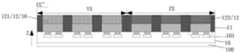
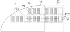
图1为本发明实施例提供的一种显示面板俯视图;FIG. 1 is a top view of a display panel provided by an embodiment of the present invention;
图2为图1S区域的一种放大图;FIG. 2 is an enlarged view of the region of FIG. 1S;
图3为图2沿剖线A-A’的一种截面示意图;Fig. 3 is a kind of sectional schematic diagram along section line A-A' of Fig. 2;
图4为图2沿剖线A-A’的另一种截面示意图;Fig. 4 is another kind of sectional schematic view along section line A-A' of Fig. 2;
图5为图1S区域的另一种放大图;Fig. 5 is another enlarged view of the region of Fig. 1S;
图6为图1S区域的又一种放大图;Fig. 6 is another enlarged view of the region of Fig. 1S;
图7为图1S区域的又一种放大图;Fig. 7 is another enlarged view of the region of Fig. 1S;
图8为图2沿剖线A-A’的又一种截面示意图;Fig. 8 is another kind of sectional schematic view along section line A-A' of Fig. 2;
图9为图2沿剖线A-A’的又一种截面示意图;Fig. 9 is another kind of cross-sectional schematic view along section line A-A' of Fig. 2;
图10为图2沿剖线A-A’的又一种截面示意图;Fig. 10 is another kind of sectional schematic view along section line A-A' of Fig. 2;
图11为图1S区域的又一种放大图;Fig. 11 is another enlarged view of the region in Fig. 1S;
图12为图11沿剖线B-B’的一种截面示意图;Fig. 12 is a kind of sectional schematic diagram along section line B-B' of Fig. 11;
图13为图11沿剖线B-B’的又一种截面示意图;Fig. 13 is another kind of sectional schematic view along section line B-B' of Fig. 11;
图14为图1S’区域的又一种放大图;Fig. 14 is another kind of enlarged view of Fig. 1S ' region;
图15为图1S区域的又一种放大图;Fig. 15 is another enlarged view of the region in Fig. 1S;
图16为图1S区域的又一种放大图;Fig. 16 is another enlarged view of the region of Fig. 1S;
图17为图16沿剖线C-C’的一种截面示意图;Fig. 17 is a kind of sectional schematic diagram along section line C-C ' of Fig. 16;
图18为图16沿剖线C-C’的又一种截面示意图;Fig. 18 is another kind of cross-sectional schematic view along section line C-C' of Fig. 16;
图19为图1S区域的又一种放大图;Fig. 19 is another enlarged view of the region in Fig. 1S;
图20为图19沿剖线D-D’的一种截面示意图;Fig. 20 is a kind of sectional schematic diagram along section line D-D' of Fig. 19;
图21为图1S区域的又一种放大图;Fig. 21 is another enlarged view of the region in Fig. 1S;
图22为图21沿剖线E-E’的一种截面示意图;Fig. 22 is a kind of sectional schematic diagram along section line E-E' of Fig. 21;
图23为图1S区域的又一种放大图;Fig. 23 is another enlarged view of the region in Fig. 1S;
图24为图23沿剖线F-F’的又一种截面示意图;Fig. 24 is another kind of cross-sectional schematic view along section line F-F' of Fig. 23;
图25为图16沿剖线C-C’的又一种截面示意图;Fig. 25 is another kind of sectional schematic view along section line C-C ' of Fig. 16;
图26为图1S区域的又一种放大图;Fig. 26 is another enlarged view of the region in Fig. 1S;
图27为图26沿剖线G-G’的又一种截面示意图;Fig. 27 is another schematic cross-sectional view of Fig. 26 along section line G-G';
图28为图2沿剖线A-A’的又一种截面示意图;Fig. 28 is another kind of cross-sectional schematic view along section line A-A' of Fig. 2;
图29为图2沿剖线A-A’的又一种截面示意图;Fig. 29 is another schematic cross-sectional view along section line A-A' of Fig. 2;
图30为图29 M区域的一种放大图;Figure 30 is an enlarged view of the M area in Figure 29;
图31为本发明实施例提供的一种显示装置的俯视图。Fig. 31 is a top view of a display device provided by an embodiment of the present invention.
具体实施方式Detailed ways
下面将结合本发明实施例中的附图,对本发明中的实施例进行清楚、完整地描述,显然,所描述的实施例仅仅是本发明一部分实施例,而不是全部的实施例。基于本发明中的实施例,本领域普通技术人员在没有做出创造性劳动前提下所获得的所有其他实施例,都属于本发明保护的范围。The embodiments of the present invention will be clearly and completely described below in conjunction with the accompanying drawings in the embodiments of the present invention. Obviously, the described embodiments are only some of the embodiments of the present invention, not all of them. Based on the embodiments of the present invention, all other embodiments obtained by persons of ordinary skill in the art without making creative efforts belong to the protection scope of the present invention.
Micro-LED作为一种新兴的显示技术,在不久的未来将逐步占领市场。随之而来的,是基于Micro-LED显示面板而形成的一系列设计应用,如圆角屏、异形屏、盲孔屏等,其需要采用不同的屏幕尺寸和外形,所以亟待技术人员能够提供一种使得异形边缘获得较好显示效果的显示面板。As an emerging display technology, Micro-LED will gradually occupy the market in the near future. What follows is a series of design applications based on Micro-LED display panels, such as rounded corner screens, special-shaped screens, blind hole screens, etc., which require different screen sizes and shapes, so technicians are urgently needed to provide A display panel that enables better display effects on special-shaped edges.
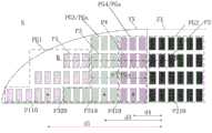
基于上述所产生的问题,本发明申请提出一种显示面板,请参照图1~2,图1为本发明实施例提供的一种显示面板俯视图,图2为图1S区域的一种放大图,如图1~2,本发明实施例提供的一种显示面板1,包括显示区AA,显示区AA包括至少一个异形区YX,如图1中的S区域S区域包括显示面板1的其中一个圆角,也就是异形区YX以及非异形区ZX,异形区YX包括第一像素单元组PG1,第一像素单元组PG1包括至少一个第一像素单元P1,非异形区ZX包括第二像素单元组PG2,第二像素单元组PG2包括至少一个第二像素单元P2。需要说明的是,图1示出的为盲孔圆角屏,其存在的异形区包括四个圆角区域以及盲孔K所在的边缘,为方便说明,图2仅以其中一个圆角(S区域)为例来说明,但其并不限制本发明的异形区域的个数,以及异形区域的形状和其位于显示面板的位置。Based on the above-mentioned problems, the present application proposes a display panel, please refer to Figures 1-2, Figure 1 is a top view of a display panel provided by an embodiment of the present invention, and Figure 2 is an enlarged view of the area in Figure 1S, As shown in Figures 1 to 2, a
如图3~4所示,图3为图1沿剖线A-A’的一种截面示意图,图4为图1沿剖线A-A’的另一种截面示意图。本发明实施例提供的一种显示面板1还包括阵列基板10,发光芯片11和量子点部12,其中阵列基板10具有衬底100和绑定端子101,发光芯片11位于阵列基板10上,且位于绑定端子101远离衬底100的一侧,所述绑定端子101用于与发光芯片11的电极进行绑定。量子点部12至少位于发光芯片11的出光面的一侧,其中量子点部12可位于封装的发光芯片11的出光面的一侧,也可位于未封装的发光芯片11的出光面的一侧;如图3所示,发光元件13位于阵列基板10上,发光元件13包括发光芯片11和位于发光芯片11外围的封装结构14,封装结构14包括封装外壳和位于封装外壳和发光芯片11之间的封装层,则量子点部12位于封装外壳和发光芯片11之间的封装层内;如图4所示,发光芯片11未封装,量子点部12位于发光芯片11出光面的一侧。本发明实施例提供的一种显示面板1,通过在发光芯片11的出光面的一侧设置量子点部12,量子点部12内具有量子点材料,量子点是在把激子在三个空间方向上束缚住的半导体纳米结构,通过对这种纳米半导体材料施加一定的电场或光压,它们便会发出特定频率的光,量子点具有良好的光稳定性,以及宽的激发谱和窄的发射谱,因此通过将量子点与发光芯片11相结合,能够优化发光芯片11的光谱成分,提高显示面板1的色彩表现力,显著提升显示面板1的色域。As shown in Figures 3 to 4, Figure 3 is a schematic cross-sectional view along the section line A-A' in Figure 1, and Figure 4 is another schematic cross-sectional view along the section line A-A' in Figure 1. A
再参照图2~4,第一像素单元P1包括至少一个发光芯片11和第一量子点部121,第二像素单元P2包括至少一个发光芯片11和第二量子点部122;且第一像素单元P1的亮度小于第二像素单元P2的亮度。通过设置第一像素单元P1的发光芯片11的出光效率小于第二像素单元P2,或者设置第一像素单元P1的量子点部12的光转换效率小于第二像素单元P2,或者上述两者调控相结合的设置方式,使得第一像素单元P1的亮度小于第二像素单元P2的亮度,使得人眼对异形边缘的可视性下降,从而弱化了异形边缘由于阵列排布的发光芯片,使得所显示的图像具有锯齿和颗粒感,从而使得显示面板的异形边缘所显示的图像具有较流畅的边界,显示面板具有良好的显示效果。2~4 again, the first pixel unit P1 includes at least one
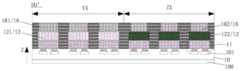
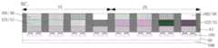
基于上述设置,可选的,如图5~6所示,图5为图1S区域的另一种放大图,图6为图1S区域的又一种放大图,可设置第一像素单元组PG1包括第一甲像素单元组PG11和第一乙像素单元组PG12,第一甲像素单元组PG11包括至少一个第一甲像素单元P11,第一乙像素单元组PG12包括至少一个第一乙像素单元P12,且第一甲像素单元P11的亮度小于第一乙像素单元P12;当第一像素单元组PG1包括多个第一像素单元P1时,多个第一像素单元P1沿着第一方向X或者第二方向Y,或者第一方向X和第二方向Y进行排布,多个第一像素单元P1沿着第一方向X排布形成像素单元行HP,多个第一像素单元P1沿着第二方向Y排布形成像素单元列VP;Based on the above settings, optionally, as shown in Figures 5-6, Figure 5 is another enlarged view of the area in Figure 1S, Figure 6 is another enlarged view of the area in Figure 1S, the first pixel unit group PG1 can be set Including the first A pixel unit group PG11 and the first B pixel unit group PG12, the first A pixel unit group PG11 includes at least one first A pixel unit P11, and the first B pixel unit group PG12 includes at least one first B pixel unit P12 , and the brightness of the first A pixel unit P11 is smaller than the first B pixel unit P12; when the first pixel unit group PG1 includes a plurality of first pixel units P1, the plurality of first pixel units P1 along the first direction X or the second Two directions Y, or the first direction X and the second direction Y are arranged, a plurality of first pixel units P1 are arranged along the first direction X to form a pixel unit row HP, and a plurality of first pixel units P1 are arranged along the second direction X The direction Y is arranged to form a pixel unit column VP;
异形区YX包括至少一段异形边缘SS’,异形边缘SS’的延伸方向与第一方向X和第二方向Y均相交;至少存在一组第一像素单元组PG1,具有与异形边缘SS’相邻的第一甲像素单元P11和第一乙像素单元P12。The special-shaped area YX includes at least one section of special-shaped edge SS', and the extension direction of the special-shaped edge SS' intersects both the first direction X and the second direction Y; there is at least one group of first pixel unit groups PG1, which have The first A pixel unit P11 and the first B pixel unit P12.
如图5和图6所示,第一像素单元组PG1具有与异形边缘SS’相邻的第一甲像素单元P11和第一乙像素单元P12,图5中,与异形边缘SS’相邻的第一乙像素单元P12位于像素单元行HP的第一行,与异形边缘SS’相邻的第一甲像素单元P11位于像素单元行HP的第二行,相比于第一像素单元P11,第二像素单元P12更靠近第二像素单元组PG2;因为沿着第二方向Y,异形区YX沿第一方向X的宽度必然经历由小至大,或者由大至小的变化;在异形区YX沿着第一方向X的宽度较大的区域,若由第二像素单元P2的亮度直接过渡到第一甲像素单元P11的亮度,可能造成非异形区ZX和异形区YX之间的亮度差异太大,从而所显示的画面容易给人造成突兀感,若由第一像素单元P2的亮度直接过渡到第一乙像素单元P12的亮度,那么可能导致异形边缘SS’可视性下降不明显,异形边缘SS’所存在的锯齿感和颗粒感仍然清晰可见,因此此设置一方面可使得非异形区ZX和异形区YX之间的亮度差异不会太大,另一方面也能有效保证显示面板的异形边缘SS’所显示的图像具有较流畅的边界。As shown in Figure 5 and Figure 6, the first pixel unit group PG1 has the first A pixel unit P11 and the first B pixel unit P12 adjacent to the special-shaped edge SS'. The first B pixel unit P12 is located in the first row of the pixel unit row HP, and the first A pixel unit P11 adjacent to the special-shaped edge SS' is located in the second row of the pixel unit row HP. Compared with the first pixel unit P11, the first pixel unit P11 The two-pixel unit P12 is closer to the second pixel unit group PG2; because along the second direction Y, the width of the special-shaped area YX along the first direction X must undergo a change from small to large, or from large to small; in the special-shaped area YX In the area with a larger width along the first direction X, if the brightness of the second pixel unit P2 directly transitions to the brightness of the first pixel unit P11, the brightness difference between the non-special-shaped area ZX and the special-shaped area YX may be too large. If the brightness of the first pixel unit P2 directly transitions to the brightness of the first B pixel unit P12, the visibility of the special-shaped edge SS' may not be significantly reduced, and the special-shaped The jaggedness and graininess existing in the edge SS' are still clearly visible, so this setting can make the brightness difference between the non-special-shaped area ZX and the special-shaped area YX not too large, and on the other hand, it can effectively ensure the brightness of the display panel. The image displayed by the profiled edge SS' has a smoother boundary.
图6中,与异形边缘SS’相邻的第一乙像素单元P12位于像素单元行HP的第二行,与异形边缘SS’相邻的第一甲像素单元P11位于像素单元行HP的第一行,相比于第二像素单元P12,第一像素单元P11更靠近异形边缘SS’的一端;因为通常越靠近异形边缘SS’的两端,由非异形区ZX至异形区YX的方向上,异形区YX所包含的像素单元的个数就越少,人眼对于所显示的图像的锯齿感和颗粒感就越强, 因此设置第一甲像素单元P11的亮度低于第一乙像素单元P12,有利于平衡异形边缘SS’的两端和中部区域的视觉效果,使得显示面板的异形边缘SS’所显示的图像具有较流畅的边界。In Fig. 6, the first B pixel unit P12 adjacent to the special-shaped edge SS' is located in the second row of the pixel unit row HP, and the first A pixel unit P11 adjacent to the special-shaped edge SS' is located in the first row of the pixel unit row HP. row, compared with the second pixel unit P12, the first pixel unit P11 is closer to one end of the special-shaped edge SS'; because usually the closer to the two ends of the special-shaped edge SS', in the direction from the non-special-shaped area ZX to the special-shaped area YX, The fewer the number of pixel units contained in the special-shaped area YX, the stronger the jaggedness and graininess of the displayed image to the human eye, so the brightness of the first A pixel unit P11 is set to be lower than that of the first B pixel unit P12 It is beneficial to balance the visual effects of the two ends and the central area of the special-shaped edge SS', so that the image displayed by the special-shaped edge SS' of the display panel has a smoother boundary.
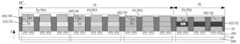
基于上述设置,可选的,如图7所示,图7为图1S区域的又一种放大图;可设置第一像素单元组PG1还包括第一丙像素单元组PG13,第一丙像素单元组PG13包括至少一个第一丙像素单元P13,且第一丙像素单元P13亮度大于第一甲像素单元P11和第一乙像素单元P12;至少存在一组第一像素单元组PG1,具有与异形边缘SS’相邻的第一甲像素单元P11、第一乙像素单元P12和第一丙像素单元P13,且第一丙像素单元P13与第一甲像素单元P11位于相同像素单元行HP或相同像素单元列VP。Based on the above settings, optionally, as shown in FIG. 7, FIG. 7 is another enlarged view of the area in FIG. 1S; The group PG13 includes at least one first C pixel unit P13, and the brightness of the first C pixel unit P13 is greater than that of the first A pixel unit P11 and the first B pixel unit P12; The first A pixel unit P11, the first B pixel unit P12, and the first C pixel unit P13 adjacent to SS', and the first C pixel unit P13 and the first A pixel unit P11 are located in the same pixel unit row HP or the same pixel unit Column VP.
如图7所示,第一像素单元组PG1具有与异形边缘SS’相邻的第一甲像素单元P11、第一乙像素单元P12和第一丙像素单元P13,图7中,与异形边缘SS’相邻的第一乙像素单元P12位于像素单元行HP的第一行,与异形边缘SS’相邻的第一甲像素单元P11和第一丙像素单元P13位于像素单元行HP的第二行,且第一乙像素单元P12的亮度在第一甲像素单元P11和第一丙像素单元P13的亮度之间,由于异形边缘SS’弧度的差异,与异形边缘SS’相邻的像素单元个数可能会存在差异,而此时与异形边缘SS’相邻的像素,位于像素单元行HP的第一行只有第一乙像素单元P12,位于像素单元行HP的第二行有第一甲像素单元P11和第一丙像素单元P13,通过设置第一乙像素单元P12的亮度在第一甲像素单元P11和第一丙像素单元P13的亮度之间,可使得第一甲像素单元P11和第一丙像素单元P13两者的综合亮度与第一乙像素单元P12的亮度差异减小,从而使得异形边缘SS’不同像素单元行HP或者不同像素单元列VP之间,亮度差异不会太大,从而使得显示面板的异形边缘SS’所显示的图像具有较流畅的边界。As shown in Figure 7, the first pixel unit group PG1 has the first A pixel unit P11, the first B pixel unit P12 and the first C pixel unit P13 adjacent to the special-shaped edge SS'. 'The adjacent first B pixel unit P12 is located in the first row of the pixel unit row HP, and the first A pixel unit P11 and the first C pixel unit P13 adjacent to the special-shaped edge SS' are located in the second row of the pixel unit row HP , and the brightness of the first B pixel unit P12 is between the brightness of the first A pixel unit P11 and the first C pixel unit P13, due to the difference in radians of the special-shaped edge SS', the number of pixel units adjacent to the special-shaped edge SS' There may be differences, and at this time, the pixels adjacent to the special-shaped edge SS' have only the first B pixel unit P12 in the first row of the pixel unit row HP, and the first A pixel unit in the second row of the pixel unit row HP P11 and the first C pixel unit P13, by setting the brightness of the first B pixel unit P12 between the brightness of the first A pixel unit P11 and the first C pixel unit P13, the first A pixel unit P11 and the first C pixel unit can be The integrated luminance of the two pixel units P13 and the luminance difference of the first B pixel unit P12 are reduced, so that the difference in luminance between different pixel unit rows HP or different pixel unit columns VP of the special-shaped edge SS' will not be too large, so that The image displayed by the special-shaped edge SS' of the display panel has a relatively smooth boundary.
需要说明的是,异形区YX采用如图5或图6或图7所示的设置方法,又或者采用图5至图7相结合的设置方法,以及像素单元所显示的具体亮度需要根据异形边缘SS’的弧度以及非异形区ZX至异形区YX边缘的宽度进行合理化设置,以使得异形边缘的显示效果较佳为准,本发明对此并不限定。It should be noted that the special-shaped area YX adopts the setting method shown in Figure 5 or Figure 6 or Figure 7, or adopts the setting method combined with Figure 5 to Figure 7, and the specific brightness displayed by the pixel unit needs to be determined according to the special-shaped edge The radian of SS' and the widths from the non-special-shaped zone ZX to the edge of the special-shaped zone YX are set rationally so that the display effect of the special-shaped edge is better, which is not limited in the present invention.
可选的,可设置第一像素单元P1的发光芯片11和第二像素单元P2的发光芯片11的发光亮度一致,设置光通过第一像素单元P1的第一量子点部121的转换效率低于光通过第二像素单元P2的第二量子点部122的转换效率,从而使得第一像素单元P1的发光芯片11通过第一量子点部121和第二像素单元P2的发光芯片11通过第二量子点部122所出射的光的强度发生差异;如可设置第一量子点部121的量子点受激发效率低于第二量子点部122的量子点受激发效率,也可设置第一量子点部121的量子点厚度小于第二量子点部122的量子点厚度,还可设置第一量子点部121的量子点密度小于第二量子点部122的量子点密度;可选的,以上所述三种方法也可两两结合使用或者三者配合使用,均可使得第一像素单元P1的亮度小于第二像素单元P2的亮度。Optionally, the luminance of the
为方便说明,以量子点部12位于未封装的发光芯片11出光面的一侧为例来说明。如图8~9所示,图8为图2沿剖线A-A’的又一种截面示意图,图9为图2沿剖线A-A’的又一种截面示意图。图8中,在垂直显示面板的方向Z上,第一量子点部121具有第一厚度H1,第二量子点部122具有第二厚度H2,且第一厚度H1小于第二厚度H2;图9中,第一量子点部121具有第一密度D1的量子点,第二量子点部122具有第二密度D2的量子点,且第一密度D1小于第二密度D2。For convenience of description, an example is taken in which the
由于量子点的光转换效率是与量子点的数量成正比的,因此当量子点部12在垂直显示面板方向Z上的投影面积一定时,发光芯片11通过厚度越大、密度越大的量子点部12时,所出射的光转换效率越高,由于第一像素单元P1所具有的量子点的数量小于第二像素单元P2,所以第一像素单元P1的亮度小于第二像素单元P2的亮度。可选的,设置第一像素单元P1的发光芯片11和第二像素单元P2的发光芯片11的发光亮度一致,只改变第一像素单元P1的量子点部12和第二像素单元P2的量子点部12的设置,可便于阵列基板10对于发光芯片11的整体调控,从而不需要特别调控位于显示面板异形边缘区域的发光芯片11的控制电压或电流,又能使得异形边缘区域的像素单元亮度下降,使得人眼对异形边缘的可视性下降,从而弱化了异形边缘由于阵列排布的发光芯片,使得所显示的图像具有锯齿和颗粒感,从而使得显示面板的异形边缘所显示的图像具有较流畅的边界,显示面板具有良好的显示效果。Since the light conversion efficiency of quantum dots is proportional to the number of quantum dots, when the projected area of the
可选的,请参照图2和图10,图10为图2沿剖线A-A’的又一种截面示意图,第一像素单元P1和第二像素单元P2均包括至少两个发光芯片11。当量子点部12位于未封装的发光芯片11出光面的一侧,第一像素单元P1还包括第一遮挡层151,第一遮挡层151位于第一像素单元P1的发光芯片11所对应的第一量子点部121之间,第二像素单元P2还包括第二遮挡层152,第二遮挡层152位于第二像素单元P2的发光芯片11所对应的第二量子点部122之间,设第一像素单元P1和第二像素单元P2的发光芯片11的排列方向为第三方向X’,第一遮挡层151沿着第三方向X’的第一宽度为B1,第二遮挡层152沿着第三方向X’的第二宽度为B2,第一宽度B1大于第二宽度B2。通过设置第一遮挡层151沿着第三方向X’的宽度大于第二遮挡层152沿着第三方向X’的宽度,则当第一像素单元P1的第一量子点部121和第二像素单元P2的第二量子点部122的厚度和密度一致时,在垂直显示面板的方向Z上,第一量子点部121的投影面积小于第二量子点部122的投影面积,此投影面积指的是可通光区域的投影面积,量子点部12的投影面积越大,则量子点部12的体积越大,量子点数量越多,也就是第一量子点部121的体积小于第二量子点部122的体积,从而使得光通过第一量子点部121的转换效率低于光通过第二量子点部122的转换效率,从而使得第一像素单元P1的亮度小于第二像素单元P2的亮度。可选的,设置第一像素单元P1的发光芯片11和第二像素单元P2的发光芯片11的发光亮度一致,第一量子点部121和第二量子点部122在垂直显示面板方向Z上的厚度一致,密度一致,只改变第一量子点部121和第二量子点部122在显示面板的正投影的面积差异,不仅便于阵列基板10对于发光芯片11的整体调控,也便于量子点的整面涂布,不需要特别调控位于显示面板异形边缘区域的发光芯片11的控制电压或电流,或者调整异形边缘区域的量子点材料和涂布工艺,又能使得异形边缘区域的像素单元亮度下降,使得人眼对异形边缘的可视性下降,从而弱化了异形边缘由于阵列排布的发光芯片,使得所显示的图像具有锯齿和颗粒感,从而使得显示面板的异形边缘所显示的图像具有较流畅的边界,显示面板具有良好的显示效果。Optionally, please refer to FIG. 2 and FIG. 10. FIG. 10 is another schematic cross-sectional view along the section line AA' in FIG. . When the
另外,通过在发光芯片11所对应的量子点部12之间设置遮挡层15,也能够有效地防止像素单元中不同芯片之间发生光的串扰,从而在一定视角上,能够保证显示面板不出现混色现象,从而改善显示面板的色偏现象。需要说明的,上述设置方法也可与量子点材料受激发效率、量子点部厚度、量子点部中量子点密度等设置方法结合起来调整异形边缘区域量子点部的变化,本发明对此并不限制,从而可根据不同量子点材料的特性和异形区域面积进行优化和选择,从而使得显示效果更好。In addition, by disposing the
可选的,当量子点部12位于封装的发光芯片11出光面的一侧,也就是位于封装外壳和发光芯片11之间的封装层内,则也可以在封装外壳内设置遮挡结构,所述遮挡结构所起的效果在于,使得量子点部12在垂直显示面板方向上的投影面积发生差异,当第一像素单元P1的第一量子点部121和第二像素单元P2的第二量子点部122的厚度和密度一致时,在垂直显示面板的方向上,第一量子点部121的投影面积小于第二量子点部122的投影面积,此投影面积指的是可通光区域的投影面积,也就是设置第一量子点部121的体积小于第二量子点部122的体积,从而使得光通过第一量子点部121的转换效率低于光通过第二量子点部122的转换效率,从而使得第一像素单元P1的亮度小于第二像素单元P2的亮度。其所起的效果也与上述方案一致,这里就不再赘述。Optionally, when the
需要说明的,以上调节方法同样适用于第一甲像素单元组PG11、第一乙像素单元组PG12和第一丙像素单元组PG13中的像素单元,像素单元调节后的亮度只要满足所表述的亮度效果即可,这里就不在进行赘述。It should be noted that the above adjustment method is also applicable to the pixel units in the first A pixel unit group PG11, the first B pixel unit group PG12 and the first C pixel unit group PG13. The effect is enough, so I won’t go into details here.
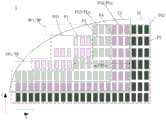
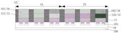
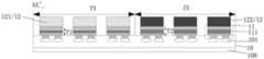
可选的,异形区YX还包括m个像素单元组PGx, m为大于等于1的正整数,3≤x≤m-2的正整数,每个像素单元组PGx包括至少一个像素单元,且m个像素单元组PGx位于第一像素单元组PG1和第二像素单元组PG2之间;请参照图11,图11为图1S区域的又一种放大图;以图11为例,异形区YX还包括2个像素单元组PG3和PG4,像素单元组PG3包括至少一个像素单元P3,像素单元组PG4包括至少一个像素单元P4,且PG3和PG4位于第一像素单元组PG1和第二像素单元组PG2之间;可选的,根据异形区域的边缘弧度和面积,可在第一像素单元组PG1和第二像素单元组PG2之间设置多个像素单元组PGx,每个像素单元组PGx也可包括多个像素单元,本发明对此不进行限定,所设置的像素单元组的个数和像素单元的个数以使得异形边缘的显示效果较佳为准。Optionally, the shaped area YX also includes m pixel unit groups PGx, m is a positive integer greater than or equal to 1, and a positive integer of 3≤x≤m-2, each pixel unit group PGx includes at least one pixel unit, and m A pixel unit group PGx is located between the first pixel unit group PG1 and the second pixel unit group PG2; please refer to FIG. 11, which is another enlarged view of the area in FIG. 1S; taking FIG. 11 as an example, the special-shaped area YX is also Including two pixel unit groups PG3 and PG4, the pixel unit group PG3 includes at least one pixel unit P3, the pixel unit group PG4 includes at least one pixel unit P4, and PG3 and PG4 are located in the first pixel unit group PG1 and the second pixel unit group PG2 between; optionally, according to the edge radian and area of the shaped area, multiple pixel unit groups PGx can be set between the first pixel unit group PG1 and the second pixel unit group PG2, and each pixel unit group PGx can also include The number of pixel units is not limited in the present invention, and the number of pixel unit groups and the number of pixel units are set so that the display effect of the irregular-shaped edge is better.
沿着第一像素单元组PG1到第二像素单元组PG2的排列方向,不同像素单元组的像素单元的亮度逐渐增大。请参照图12,图12为图11沿剖线B-B’的一种截面示意图;以图12为例,沿着第一像素单元组PG1到第二像素单元组PG2的排列方向上,依次设置第一像素单元组PG1、像素单元组PG3、像素单元组 PG4和第二像素单元组PG2,第一像素单元组PG1包括一个第一像素单元P1,像素单元组PG3包括一个像素单元P3,像素单元组PG4包括一个像素单元P4,第二像素单元组PG2包括一个第二像素单元P2,第一像素单元P1到第二像素单元P2的亮度逐渐增大,也就是第一像素单元P1亮度小于像素单元P3亮度,像素单元P3亮度小于像素单元P4亮度,像素单元P4亮度小于第二像素单元P2亮度。通过在第一像素单元组PG1和第二像素单元组PG2之间设置过渡亮度的像素单元组,使得异形边缘所显示的图像更加自然和细腻,从而进一步改善异形屏幕的显示效果。Along the arrangement direction of the first pixel unit group PG1 to the second pixel unit group PG2, the brightness of the pixel units of different pixel unit groups increases gradually. Please refer to Figure 12, which is a schematic cross-sectional view of Figure 11 along the section line BB'; taking Figure 12 as an example, along the arrangement direction from the first pixel unit group PG1 to the second pixel unit group PG2, sequentially Set the first pixel unit group PG1, the pixel unit group PG3, the pixel unit group PG4 and the second pixel unit group PG2, the first pixel unit group PG1 includes a first pixel unit P1, the pixel unit group PG3 includes a pixel unit P3, and the pixel The unit group PG4 includes a pixel unit P4, and the second pixel unit group PG2 includes a second pixel unit P2. The brightness of the first pixel unit P1 to the second pixel unit P2 gradually increases, that is, the brightness of the first pixel unit P1 is smaller than that of the pixel unit P1. The brightness of the unit P3, the brightness of the pixel unit P3 is smaller than the brightness of the pixel unit P4, and the brightness of the pixel unit P4 is smaller than the brightness of the second pixel unit P2. By setting a pixel unit group with transition brightness between the first pixel unit group PG1 and the second pixel unit group PG2, the image displayed on the edge of the special shape is more natural and delicate, thereby further improving the display effect of the special-shaped screen.
可选的,可设置相同的像素单元组中像素单元的亮度一致,请继续参照图11,以图11中第三行的像素单元的排列为例,沿着第一像素单元组PG1到第二像素单元组PG2的排列方向上,依次设置第一像素单元组PG1、像素单元组PG3、像素单元组 PG4和第二像素单元组PG2,第一像素单元组PG1包括两个第一像素单元P1,像素单元组PG3包括一个像素单元P3,像素单元组PG4包括一个像素单元P4,第二像素单元组PG2包括两个第二像素单元P2,则在第一像素单元组PG1中,可设置两个第一像素单元P1的亮度一致,此设置便于统一调控像素单元组内的像素单元,调控更加简便可行;可选的,也可设置相同的像素单元组中的像素单元的亮度不一致,且沿着第一像素单元组PG1到第二像素单元组PG2的排列方向上,亮度逐渐增大,此设置在相同的像素单元组中再进行一定的亮度过渡,从而使得异形边缘所呈现的图像更加自然,细腻程度更加良好,显示效果更加出众。Optionally, the brightness of the pixel units in the same pixel unit group can be set to be the same. Please continue to refer to FIG. 11, taking the arrangement of the pixel units in the third row in FIG. In the arrangement direction of the pixel unit group PG2, the first pixel unit group PG1, the pixel unit group PG3, the pixel unit group PG4 and the second pixel unit group PG2 are sequentially arranged, and the first pixel unit group PG1 includes two first pixel units P1, The pixel unit group PG3 includes one pixel unit P3, the pixel unit group PG4 includes one pixel unit P4, and the second pixel unit group PG2 includes two second pixel units P2, then in the first pixel unit group PG1, two second pixel units can be set The brightness of a pixel unit P1 is consistent, this setting is convenient for uniform regulation of the pixel units in the pixel unit group, and the regulation is more convenient and feasible; optional, it is also possible to set the brightness of the pixel units in the same pixel unit group to be inconsistent, and along the first In the arrangement direction from the first pixel unit group PG1 to the second pixel unit group PG2, the brightness gradually increases. This setting makes a certain brightness transition in the same pixel unit group, so that the image presented by the special-shaped edge is more natural and delicate. The degree is better, and the display effect is more outstanding.
可选的,设置第一像素单元组PG1和m个像素单元组PGx中的像素单元沿第一方向X或者第二方向Y或者第一方向X和第二方向Y排布,像素单元沿着第一方向X排布形成像素单元行HP,沿第二方向Y排布形成像素单元列VP,沿着第一像素单元组PG1到第二像素单元组PG2的排列方向,至少存在两行像素单元行HP,或者,至少存在两列像素单元列VP,或者至少存在一行像素单元行HP与一列像素单元列VP,其所包括的像素单元组的个数、像素单元组中像素单元的个数以及像素单元的亮度都一致。Optionally, the pixel units in the first pixel unit group PG1 and the m pixel unit groups PGx are arranged along the first direction X or the second direction Y or the first direction X and the second direction Y, and the pixel units are arranged along the second direction One direction X is arranged to form pixel unit rows HP, and the second direction Y is arranged to form pixel unit columns VP. Along the arrangement direction from the first pixel unit group PG1 to the second pixel unit group PG2, there are at least two rows of pixel unit rows HP, or at least two columns of pixel unit columns VP, or at least one row of pixel unit rows HP and one column of pixel unit columns VP, the number of pixel unit groups included, the number of pixel units in the pixel unit group, and the number of pixels The brightness of the units are all consistent.
如图1和14所示,图14为图1S’区域的又一种放大图;如图1,本发明实施例提供的一种显示面板1,其存在的异形区YX还包括盲孔K所在的边缘(S’区域),以下针对盲孔K所形成的圆形边缘的一部分进行举例说明,如图14中,第一像素单元组PG1和m个像素单元组PGx中的像素单元沿第一方向X和第二方向Y排布,存在四组像素单元行HP,沿着第一像素单元组PG1到第二像素单元组PG2的排列方向,异形区YX所包括的像素单元组的个数、像素单元组中像素单元的个数以及像素单元的亮度都一致,如第一行像素单元行HP和第八行像素单元行,其所包括的像素单元组的个数均为三组,分别为像素单元组PG4、像素单元组PG3和第一像素单元组PG1,且每组像素单元组中的像素单元的个数也一致,像素单元组PG4均包括两个像素单元P4,像素单元组PG3均包括一个像素单元P3,第一像素单元组PG1均包括两个第一像素单元P1;由于此异形区YX为盲孔K的圆形边缘的一部分,圆形为规则图形,其具有在显示面板1所在的平面上沿着任意方向的对称轴,如图14所示,假设虚线OO’为盲孔K所在的圆形边缘沿着第一方向X的对称轴,则在对称轴OO’的上下侧,其异形边缘的弧度和长度均是一致,是以对称轴OO’为基准线形成的镜像对称图,此时在对称轴OO’的上下侧,设置镜像对称的像素单元组、像素单元,并且像素单元所显示的亮度也是对称的,不仅便于盲孔K所在的异形边缘的设置,也使得圆孔周围的显示效果均一。As shown in Figures 1 and 14, Figure 14 is another enlarged view of the area of Figure 1S'; as shown in Figure 1, a
需要说明的是,上述以盲孔K所在的异形边缘为例进行说明,但此设置不仅仅应用于盲孔异形边缘,也可用于其他相对规则图形的异形边缘,如跑道孔、水滴孔、手表圆边等,也可用于其他不规则图形的异形边缘,如异形边缘存在弧度相似,且与非异形区的距离基本一致的区域,也可以采用上述的设置方式,且不仅可以应用于像素单元行HP,也可以应用于像素单元列VP。It should be noted that the above description takes the special-shaped edge where the blind hole K is located as an example, but this setting is not only applied to the special-shaped edge of the blind hole, but also can be used for other relatively regular shaped edges, such as runway holes, water drop holes, watch holes, etc. Rounded edges, etc., can also be used for other irregularly shaped edges. For example, if the irregularly shaped edge has similar radians and is basically the same distance from the non-shaped area, the above setting method can also be used, and it can not only be applied to pixel unit rows HP, can also be applied to the pixel cell column VP.
可选的,如图15,图15为图1S区域的又一种放大图;第一像素单元组PG1和m个像素单元组PGx中的像素单元沿第一方向X和第二方向Y排布,沿着第一像素单元组PG1到第二像素单元组PG2的排列方向,每个像素单元行HP所包括的像素单元组的个数、像素单元组中像素单元的个数以及像素单元的亮度均有像素单元列VP与其一致,以像素单元行HP1和像素单元列VP1为例进行说明,在像素单元行HP1中,异形区YX具有两组像素单元组,分别为像素单元组PG3和像素单元组PG4,在像素单元列VP1中,异形区YX也具有两组像素单元组,分别为像素单元组PG3和像素单元组PG4;在像素单元行HP1中,像素单元组PG3和像素单元组PG4分别包含一个像素单元,在像素单元列VP1中,像素单元组PG3和像素单元组PG4也分别包含一个像素单元,且像素单元行HP1和像素单元列VP1中的像素单元P3和像素单元P4亮度一致;如此设置不仅便于圆角所在的异形边缘的设置,也使得圆角两端的显示效果均一,此设置方式可适用于圆角两端异形边缘的弧度较一致,且与非异形区的距离也基本一致;也可适用于其他异形边缘,需要根据异形边缘的弧度、长度以及与非异形区的距离进行合理设置。Optionally, as shown in Figure 15, Figure 15 is another enlarged view of the area in Figure 1S; the pixel units in the first pixel unit group PG1 and the m pixel unit groups PGx are arranged along the first direction X and the second direction Y , along the arrangement direction from the first pixel unit group PG1 to the second pixel unit group PG2, the number of pixel unit groups included in each pixel unit row HP, the number of pixel units in the pixel unit group, and the brightness of the pixel unit Both have the same pixel unit column VP, and take the pixel unit row HP1 and the pixel unit column VP1 as an example to illustrate. In the pixel unit row HP1, the special-shaped area YX has two sets of pixel unit groups, which are pixel unit group PG3 and pixel unit group Group PG4, in the pixel unit column VP1, the special-shaped area YX also has two sets of pixel unit groups, respectively pixel unit group PG3 and pixel unit group PG4; in the pixel unit row HP1, pixel unit group PG3 and pixel unit group PG4 respectively Including one pixel unit, in the pixel unit column VP1, the pixel unit group PG3 and the pixel unit group PG4 also respectively include a pixel unit, and the pixel unit P3 and the pixel unit P4 in the pixel unit row HP1 and the pixel unit column VP1 have the same brightness; This setting not only facilitates the setting of the special-shaped edge where the rounded corner is located, but also makes the display effect at both ends of the rounded corner uniform. This setting method can be applied to the arcs of the special-shaped edge at both ends of the rounded corner are relatively consistent, and the distance from the non-special-shaped area is also basically the same. ; It can also be applied to other special-shaped edges, and it needs to be set reasonably according to the radian, length and distance from the non-special-shaped area of the special-shaped edge.
可选的,m个像素单元组的每个像素单元均包括至少一个发光芯片11和量子点部12,可选的,沿着第一像素单元组PG1到第二像素单元组PG2的排列方向上,不同像素单元组的量子点部12在垂直显示面板方向Z上的厚度逐渐增大;如图13所示,图13为图11沿剖线B-B’的又一种截面示意图;在垂直显示面板方向Z上,第一像素单元P1的第一量子点部121的厚度为H1,像素单元P3的量子点部12的厚度为H3,像素单元P4的量子点部12的厚度为H4,第二像素单元P2的第二量子点部122的厚度为H2,则H1<H3<H4<H2,沿着第一像素单元组PG1到第二像素单元组PG2的排列方向上,通过设置不同像素单元组的量子点部的厚度逐渐增大,可以使得不同像素单元组的像素单元的亮度逐渐增大,从而使得异形边缘所显示的图像更加自然和细腻,提升显示效果。Optionally, each pixel unit of the m pixel unit groups includes at least one light-emitting
可选的,沿着第一像素单元组PG1到第二像素单元组PG2的排列方向上,不同像素单元组的量子点部12的量子点密度逐渐增大;请参考图12,第一像素单元P1的第一量子点部121的量子点密度为D1,像素单元P3的量子点部12的量子点密度为D3,像素单元P4的量子点部12的量子点密度为D4,第二像素单元P2的第二量子点部122的量子点密度为D2,则D1<D3<D4<D2,沿着第一像素单元组PG1到第二像素单元组PG2的排列方向上,通过设置不同像素单元组的量子点部的量子点密度逐渐增大,可以使得不同像素单元组的像素单元的亮度逐渐增大,从而使得异形边缘所显示的图像更加自然和细腻,提升显示效果。Optionally, along the arrangement direction from the first pixel unit group PG1 to the second pixel unit group PG2, the quantum dot density of the
可选的,若不同像素单元组还包括遮挡层,所述遮挡层位于像素单元组的发光芯片所对应的量子点部之间,沿着第一像素单元组PG1到第二像素单元组PG2的排列方向上,也可设置不同像素单元组的遮挡层的宽度逐渐减小,从而使得不同像素单元组的量子点部的体积逐渐增大,也可使得不同像素单元组的像素单元的亮度逐渐增大,使得异形边缘所显示的图像更加自然和细腻,提升显示效果。可选的,上述方法也可结合使用,以便于灵活调整异形边缘的亮度设置,使得异形边缘的过渡更加顺畅。Optionally, if different pixel unit groups further include a shielding layer, the shielding layer is located between the quantum dots corresponding to the light-emitting chips of the pixel unit group, along the first pixel unit group PG1 to the second pixel unit group PG2 In the arrangement direction, the width of the shielding layer of different pixel unit groups can also be set to gradually decrease, so that the volume of the quantum dot portion of different pixel unit groups gradually increases, and the brightness of the pixel units of different pixel unit groups can also be gradually increased. Larger, making the image displayed by the special-shaped edge more natural and delicate, and improving the display effect. Optionally, the above methods may also be used in combination, so as to flexibly adjust the brightness setting of the special-shaped edge, so that the transition of the special-shaped edge is smoother.
可选的,第i个像素单元组的一个像素单元的亮度为Li,第一像素单元P1的亮度为L1,1≤i≤m-2,且i为不等于2的正整数;沿着所述第一像素单元组到所述第二像素单元组的排列方向,所述第一像素单元组中距离所述第二像素单元组最近的所述第一像素单元为第一子像素单元,所述第二像素单元组中距离所述第一像素组最近所述第二像素单元为第二子像素单元,所述第一子像素单元的中心与所述第二子像素单元的中心距离为d1;Optionally, the brightness of a pixel unit of the i-th pixel unit group is Li, the brightness of the first pixel unit P1 is L1, 1≤i≤m-2, and i is a positive integer not equal to 2; along the The arrangement direction from the first pixel unit group to the second pixel unit group, the first pixel unit closest to the second pixel unit group in the first pixel unit group is the first sub-pixel unit, so The second pixel unit closest to the first pixel group in the second pixel unit group is a second sub-pixel unit, and the distance between the center of the first sub-pixel unit and the center of the second sub-pixel unit is d1 ;
所述第i个像素单元组中距离所述第二像素单元组最近的所述像素单元为第i个子像素单元,所述第i个子像素单元的中心与所述第二子像素单元的中心的距离为di;则Li/L1反比于di/d1。The pixel unit closest to the second pixel unit group in the i-th pixel unit group is the i-th sub-pixel unit, and the distance between the center of the i-th sub-pixel unit and the center of the second sub-pixel unit The distance is di; then Li/L1 is inversely proportional to di/d1.
请继续参考图11,以图11中第四行的像素单元的排列为例,沿着第一像素单元组PG1到第二像素单元组PG2的排列方向上,依次设置第一像素单元组PG1、第三像素单元组PG3、第四像素单元组 PG4和第二像素单元组PG2,第一像素单元组PG1包括两个第一像素单元P1,第三像素单元组PG3包括两个像素单元P3,第四像素单元组PG4包括一个像素单元P4,第二像素单元组PG2包括两个第二像素单元P2。Please continue to refer to FIG. 11. Taking the arrangement of the pixel units in the fourth row in FIG. 11 as an example, along the arrangement direction from the first pixel unit group PG1 to the second pixel unit group PG2, the first pixel unit group PG1, the second pixel unit group PG2 are sequentially arranged. The third pixel unit group PG3, the fourth pixel unit group PG4 and the second pixel unit group PG2. The first pixel unit group PG1 includes two first pixel units P1. The third pixel unit group PG3 includes two pixel units P3. The four pixel unit group PG4 includes one pixel unit P4, and the second pixel unit group PG2 includes two second pixel units P2.
其中,第一像素单元P1的亮度为L1 ,第三像素单元组PG3的一个像素单元P3的亮度为L3,第四像素单元组PG4的一个像素单元的亮度为L4,沿着第一像素单元组PG1到第二像素单元组PG2的排列方向上,第一像素单元组PG1中距离第二像素单元组PG2最近的第一像素单元P1为第一子像素单元P110,第三像素单元组PG3中距离第二像素单元组PG2最近的像素单元P3为第三子像素单元P310,第四像素单元组PG4中距离第二像素单元组PG2最近的像素单元P4为第四子像素单元P410,第二像素单元组PG2中距离第一像素单元组PG1最近的第二像素单元P2为第二子像素单元P210,则第一子像素单元P110的中心与第二子像素单元P210的中心距离为d1,第三子像素单元P310的中心与第二子像素单元P210的中心距离为d3,第四子像素单元P410的中心与第二子像素单元P210的中心距离为d4,则L3/L1相比L4/L1增加的幅值,反比于d3/d1相比d4/d1减小的幅值。Wherein, the brightness of the first pixel unit P1 is L1, the brightness of one pixel unit P3 of the third pixel unit group PG3 is L3, and the brightness of one pixel unit of the fourth pixel unit group PG4 is L4, along the first pixel unit group In the arrangement direction from PG1 to the second pixel unit group PG2, the first pixel unit P1 closest to the second pixel unit group PG2 in the first pixel unit group PG1 is the first sub-pixel unit P110, and the distance between the third pixel unit group PG3 The pixel unit P3 closest to the second pixel unit group PG2 is the third sub-pixel unit P310, the pixel unit P4 closest to the second pixel unit group PG2 in the fourth pixel unit group PG4 is the fourth sub-pixel unit P410, and the second pixel unit The second pixel unit P2 closest to the first pixel unit group PG1 in the group PG2 is the second sub-pixel unit P210, then the distance between the center of the first sub-pixel unit P110 and the center of the second sub-pixel unit P210 is d1, and the third sub-pixel unit The distance between the center of the pixel unit P310 and the center of the second sub-pixel unit P210 is d3, and the distance between the center of the fourth sub-pixel unit P410 and the center of the second sub-pixel unit P210 is d4, then L3/L1 is increased compared to L4/L1 Amplitude, inversely proportional to d3/d1 compared to d4/d1 reduced amplitude.
可选的,Li/L1=k(di/d1)+b,k<0,b>0,也就是Li/L1与di/d1呈线性的反比,此设置可以使得异形边缘的亮度减小随着距离的增加呈现线性的规律性变化,从而使得异形区到非异形区的过渡更加自然。可选的,Li/L1与di/d1的反比也可为指数型、幂函数、多项式等的渐变,此设置可以使得异形边缘的亮度减小随着距离的增加呈现一定的规律性变化,对于不同的弧度的异形边缘以及异形区域的面积大小,可以选择不同的规律性去调整异形边缘的像素亮度,从而使得异形区到非异形区的过渡更加自然。Optionally, Li/L1=k(di/d1)+b, k<0, b>0, that is, Li/L1 is linearly inversely proportional to di/d1, this setting can reduce the brightness of the special-shaped edge with the As the distance increases, it presents a linear regular change, which makes the transition from the abnormal-shaped area to the non-alien-shaped area more natural. Optionally, the inverse ratio of Li/L1 to di/d1 can also be a gradual change of exponential type, power function, polynomial, etc. This setting can make the brightness of the special-shaped edge decrease with a certain regularity as the distance increases. For With different radians of shaped edges and the size of the shaped area, different regularities can be selected to adjust the pixel brightness of the shaped edge, so that the transition from the shaped area to the non-shaped area is more natural.
可选的,设置第二像素单元P2的亮度为L2,则沿着第一像素单元组PG1到第二像素单元组PG2的排列方向,相邻两个像素单元的亮度差异<L2×78%。继续参照图11,继续以图11中第四行的像素单元的排列为例,沿着第一像素单元组PG1到第二像素单元组PG2的排列方向上,依次设置第一像素单元组PG1、第三像素单元组PG3、第四像素单元组 PG4和第二像素单元组PG2,第一像素单元组PG1包括两个第一像素单元P1,第三像素单元组PG3包括两个像素单元P3,第四像素单元组PG4包括一个像素单元P4,第二像素单元组PG2包括两个第二像素单元P2。Optionally, if the brightness of the second pixel unit P2 is set as L2, along the arrangement direction from the first pixel unit group PG1 to the second pixel unit group PG2, the difference in brightness between two adjacent pixel units is <L2×78%. Continue referring to FIG. 11 , continue to take the arrangement of the pixel units in the fourth row in FIG. 11 as an example, along the arrangement direction from the first pixel unit group PG1 to the second pixel unit group PG2, sequentially arrange the first pixel unit group PG1, The third pixel unit group PG3, the fourth pixel unit group PG4 and the second pixel unit group PG2. The first pixel unit group PG1 includes two first pixel units P1. The third pixel unit group PG3 includes two pixel units P3. The four pixel unit group PG4 includes one pixel unit P4, and the second pixel unit group PG2 includes two second pixel units P2.
其中,第一像素单元组PG1与第三像素单元组PG3相邻的像素单元为第一子像素单元P110和像素单元P320,第三像素单元组PG3与第四像素单元组PG4相邻的像素单元为第三子像素单元P310和第四子像素单元P410,第四像素单元组PG4与第二像素单元组PG2相邻的像素单元为第四子像素单元P410和第二子像素单元P210,则像素单元P110和P320之间,像素单元P310和P410之间,以及像素单元P410和P210之间的亮度差值的绝对值,均要小于第二像素单元P2的亮度L2的78%。Among them, the pixel units adjacent to the first pixel unit group PG1 and the third pixel unit group PG3 are the first sub-pixel unit P110 and the pixel unit P320, and the pixel units adjacent to the third pixel unit group PG3 and the fourth pixel unit group PG4 is the third sub-pixel unit P310 and the fourth sub-pixel unit P410, and the pixel units adjacent to the fourth pixel unit group PG4 and the second pixel unit group PG2 are the fourth sub-pixel unit P410 and the second sub-pixel unit P210, then the pixel The absolute values of the brightness differences between the units P110 and P320, between the pixel units P310 and P410, and between the pixel units P410 and P210 are all less than 78% of the brightness L2 of the second pixel unit P2.
由非异形区到异形区进行显示亮度的过渡,体现为由非异形区到异形区的亮度递减,而通过视觉效果的反复验证,相邻两个像素单元的亮度差小于非异形区的78%,所显示的图像不会因亮度差异过大出现不自然的现象。The transition of display brightness from the non-special-shaped area to the special-shaped area is reflected in the gradual decrease of brightness from the non-special-shaped area to the special-shaped area, and through repeated verification of visual effects, the brightness difference between two adjacent pixel units is less than 78% of the non-special-shaped area , the displayed image will not appear unnatural due to excessive brightness differences.
可选的,设置不同像素单元组包括的发光芯片11亮度一致,相邻两个像素单元所对应的量子点部12在垂直显示面板方向Z上面积一致,所包含的量子点密度也一致的条件下,量子点部12的厚度为甲厚度和乙厚度,则甲厚度和乙厚度的差异也需要满足,光通过甲厚度和乙厚度的量子点部12的亮度差值的绝对值小于第二像素单元P2的亮度L2的78%。Optionally, set the conditions that the light-emitting
可选的,设置不同像素单元组包括的发光芯片11亮度一致,相邻两个像素单元所对应的量子点部12在垂直显示面板方向Z上面积一致,厚度一致的条件下,量子点部12所具有的量子点密度为甲密度和乙密度,则甲密度和乙密度的差异也需要满足,光通过甲密度和乙密度的量子点部12的亮度差值的绝对值小于第二像素单元P2的亮度L2的78%。Optionally, the brightness of the light-emitting
可选的,通过对量子点部12进行单一变量的调控,更容易保证相邻两个像素单元所对应的亮度差异不会太大,不会因亮度差异过大出现不自然的现象。Optionally, by adjusting the single variable of the
可选的,本发明实施例所提供的一种发光芯片为蓝光微米级发光二极管,其普遍应用于各种显示面板和显示装置。Optionally, a light-emitting chip provided by an embodiment of the present invention is a blue micron-scale light-emitting diode, which is generally applied to various display panels and display devices.
可选的,如图16所示,图16为图1S区域的又一种放大图,图17为图16沿剖线C-C’的一种截面示意图;本发明实施例提供的一种显示面板1还包括色阻层16,且色阻层16与发光芯片11在垂直显示面板的方向Z上的投影至少部分交叠,当量子点部12位于未封装的发光芯片11出光面的一侧,量子点部12位于色阻层16内,也就是量子点是掺杂于色阻层内16的,则通过调整色阻层16在垂直显示面板方向Z上的厚度以及色阻层16在垂直显示面板方向Z上的投影面积,也就是调整量子点部12在垂直显示面板方向Z上的厚度以及量子点部12在垂直显示面板方向Z上的投影面积,则通过一次设置调整,就可以实现色阻层16和量子点部12同时调整,从而更有效地优化异形边缘区域的像素单元亮度,使得异形边缘区域的像素单元亮度下降,使得人眼对异形边缘的可视性下降,从而弱化了异形边缘由于阵列排布的发光芯片,使得所显示的图像具有锯齿和颗粒感,从而使得显示面板的异形边缘所显示的图像具有较流畅的边界,显示面板具有良好的显示效果。Optionally, as shown in FIG. 16, FIG. 16 is another enlarged view of the area in FIG. 1S, and FIG. 17 is a schematic cross-sectional view of FIG. 16 along the section line CC'; a display provided by an embodiment of the present invention The
可选的,如图18所示,图18为图16沿剖线C-C’的又一种截面示意图;色阻层16位于量子点部12远离所述阵列基板10的一侧,且色阻层16与发光芯片11在垂直显示面板的方向Z上的投影至少部分交叠,其可以使得显示面板的色域更加宽广,显示图片的色彩更加丰富。Optionally, as shown in FIG. 18, FIG. 18 is another schematic cross-sectional view along the section line CC' in FIG. 16; The
可选的,如图19~20所示,图19为图1S区域的又一种放大图,图20为图19沿剖线D-D’的一种截面示意图;色阻层16位于量子点部12远离所述阵列基板10的一侧,第一像素单元P1包括第一色阻层161,第二像素单元P2包括第二色阻层162,在垂直显示面板的方向Z上,第一色阻层161的投影具有第一面积s1,第二色阻层162的投影具有第二面积s2,第一面积s1大于第二面积s2。由于通过色阻层16的光具有特定的波长范围,因此色阻层16具有滤光的作用,通过色阻层16的光强会减弱,通过设置第一像素单元P1的第一色阻层161在垂直显示面板方向Z上的投影面积大于第二像素单元P2的第二色阻层162在垂直显示面板方向Z上的投影面积,则相比第一色阻层161,因为有更多光不需要通过第二色阻层162,所以使得通过第二色阻层162的光强要更大,也可使得第一像素单元P1的亮度小于第二像素单元P2的亮度。通过设置第一像素单元P1的亮度小于第二像素单元P2的亮度,使得人眼对异形边缘的可视性下降,从而弱化了异形边缘由于阵列排布的发光芯片,使得所显示的图像具有锯齿和颗粒感,从而使得显示面板的异形边缘所显示的图像具有较流畅的边界,显示面板具有良好的显示效果。Optionally, as shown in Figures 19-20, Figure 19 is another enlarged view of the region of Figure 1S, and Figure 20 is a schematic cross-sectional view of Figure 19 along the section line DD'; the color-resisting
可选的,异形区YX还包括m个像素单元组PGx, m为大于等于1的正整数,3≤x≤m-2的正整数,每个像素单元组PGx包括至少一个像素单元,且m个像素单元组PGx位于第一像素单元组PG1和第二像素单元组PG2之间。如图16所示,图16为图1S区域的又一种放大图,异形区YX包括2个像素单元组PG3和PG4,像素单元组PG3包括至少一个像素单元P3,像素单元组PG4包括至少一个像素单元P4,且PG3和PG4位于第一像素单元组PG1和第二像素单元组PG2之间。Optionally, the shaped area YX also includes m pixel unit groups PGx, m is a positive integer greater than or equal to 1, and a positive integer of 3≤x≤m-2, each pixel unit group PGx includes at least one pixel unit, and m A pixel unit group PGx is located between the first pixel unit group PG1 and the second pixel unit group PG2. As shown in Figure 16, Figure 16 is another enlarged view of the area in Figure 1S, the special-shaped area YX includes two pixel unit groups PG3 and PG4, the pixel unit group PG3 includes at least one pixel unit P3, and the pixel unit group PG4 includes at least one The pixel unit P4, and PG3 and PG4 are located between the first pixel unit group PG1 and the second pixel unit group PG2.
m个像素单元组的每个像素单元均包括至少一个发光芯片11、量子点部12和色阻层16,沿着第一像素单元组PG1到第二像素单元组PG2的排列方向上,不同像素单元组所对应的色阻层16在垂直显示面板方向Z上的投影面积逐渐减小;如图21~22所示,图22为图21沿剖线E-E’的一种截面示意图;在垂直显示面板方向Z上,第一像素单元P1所对应的第一色阻层161的投影面积为s1,像素单元P3所对应的色阻层16为第三色阻层163,其投影面积为s3,像素单元P4所对应的色阻层16为第四色阻层164,其投影面积为s3,第二像素单元P2所对应的第一色阻层162的投影面积为s2,则是s1>s3>s4>s2,沿着第一像素单元组PG1到第二像素单元组PG2的排列方向上,通过设置不同像素单元组所对应的色阻层在垂直显示面板方向上的投影面积逐渐减小,可以使得不同像素单元组的像素单元的亮度逐渐增大,从而使得异形边缘所显示的图像更加自然和细腻,提升显示效果。可选的,上述方案也可以结合量子点部12的一系列设计进行配合调整,如图22所示,沿着第一像素单元组PG1到第二像素单元组PG2的排列方向上,不同像素单元组所对应的色阻层16在垂直显示面板方向Z上的投影面积逐渐减小的设置结合了不同像素单元组所对应的量子点部12的量子点密度逐渐变大的设置,两种设置共同对异形区域的像素单元的亮度进行调整,从而使得异形边缘所显示的图像更加自然和细腻,提升显示效果。Each pixel unit of the m pixel unit groups includes at least one light-emitting
可选的,沿着第一像素单元组PG1到第二像素单元组PG2的排列方向上,也可设置不同像素单元组所对应的色阻层16在垂直显示面板方向Z上的厚度逐渐减小;如图23~24所示,图23为图1S区域的又一种放大图,图24为图23沿剖线F-F’的又一种截面示意图。在垂直显示面板方向Z上,第一像素单元P1所对应的第一色阻层161的厚度为h1,像素单元P3所对应的色阻层16为第三色阻层163,其厚度为h3,像素单元P4所对应的色阻层16为第四色阻层164,其厚度为h4,第二像素单元P2所对应的第一色阻层162的厚度为h2,则是h1>h3>h4>h2,沿着第一像素单元组PG1到第二像素单元组PG2的排列方向上,通过设置不同像素单元组所对应的色阻层在垂直显示面板方向上的厚度逐渐减小,也可以使得不同像素单元组的像素单元的亮度逐渐增大,从而使得异形边缘所显示的图像更加自然和细腻,提升显示效果。可选的,上述方案也可以结合色阻层16在垂直显示面板上的投影面积渐变和量子点部12的一系列设计进行配合调整,如图24所示,沿着第一像素单元组PG1到第二像素单元组PG2的排列方向上,不同像素单元组所对应的色阻层16在垂直显示面板方向Z上的厚度逐渐减小的设置结合了不同像素单元组所对应的量子点部12的量子点密度逐渐变大的设置,两种设置共同对异形区域的像素单元的亮度进行调整,从而使得异形边缘所显示的图像更加自然和细腻,提升显示效果。Optionally, along the arrangement direction from the first pixel unit group PG1 to the second pixel unit group PG2, the thickness of the color-resist
可选的,如图25所示,图25为图16沿剖线C-C’的又一种截面示意图;第一像素单元P1和第二像素单元P2均包括至少三个发光芯片11,且发光芯片11透过其分别对应的量子点部12所发出的光分别为红光、绿光和蓝光,可选的,其中发出蓝光的子像素所对应的发光芯片11的出光面不设置量子点部12。Optionally, as shown in FIG. 25, FIG. 25 is another schematic cross-sectional view along the section line CC' in FIG. 16; both the first pixel unit P1 and the second pixel unit P2 include at least three light-emitting
可选的,如图26~27所示,图26为图1S区域的又一种放大图,图27为图26沿剖线G-G’的又一种截面示意图;第一像素单元P1和第二像素单元P2均具有四个发光芯片11,且发光芯片11透过其分别对应所述量子点部12所发出的光分别为红光、绿光、蓝光和第四颜色光,第四颜色光可为白光或黄光。Optionally, as shown in FIGS. 26-27, FIG. 26 is another enlarged view of the area in FIG. 1S, and FIG. 27 is another schematic cross-sectional view along the section line G-G' in FIG. 26; the first pixel unit P1 and The second pixel unit P2 has four light-emitting
可选的,可设置第一像素单元P1的发光芯片11和第二像素单元P2的发光芯片11的自身发光效率不一致,第一像素单元P1的发光芯片11的发光效率低于第二像素单元P2的发光芯片11,可设置的方法包括:设置第一像素单元P1的发光芯片11的发光层厚度小于第二像素单元P2的发光芯片11的发光层厚度;设置第一像素单元P1的发光芯片11的发光层具有x个掺杂层,第二像素单元P2的发光芯片11的发光层具有y个掺杂层,且x<y;也可以通过设置发光芯片11的发光层中所掺杂的材料组分不一致,来设置第一像素单元P1的发光芯片11的发光效率低于第二像素单元P2的发光芯片11。可选的,以上三种发光芯片的设置方法,可以单独应用,也可以结合应用,本发明对此不做限定。可选的,对于设置第一像素单元P1的发光芯片11和第二像素单元P2的发光芯片11的自身发光效率不一致,也可结合量子点部12、色阻层16的一系列设置方式配合调整异形区至非异形区多个像素单元的亮度,从而使得异形边缘所显示的图像更加自然和细腻,提升显示效果。Optionally, the luminous efficiency of the light-emitting
如图28~30所示,图28为图2沿剖线A-A’的又一种截面示意图,图29为图2沿剖线A-A’的又一种截面示意图,图30为图29 M区域的一种放大图;图28中,发光芯片11具有发光层111,第一像素单元P1的发光芯片11的发光层111厚度为T1,第二像素单元P2的发光芯片11的发光层111厚度为T2,则T1小于T2;图29~30中,发光芯片11具有发光层111,且发光层111具有掺杂层112,第一像素单元P1的发光芯片11的发光层111具有2个掺杂层112,第二像素单元P2的发光芯片11的发光层111具有3个掺杂层113;由于发光芯片11的发光层111为多量子阱结构,多量子阱结构包含多个掺杂层,多量子阱结构能够加强载流子的限制作用,提高发光芯片11的空穴和电子的复合效率,从而提升发光芯片11的辐射效率,因此当发光芯片11的发光层111厚度增加,掺杂层数增加时,其发光芯片11的发光效率是提升的,所以当设置第一像素单元P1的发光芯片11的发光层厚度小于第二像素单元P2的发光芯片11的发光层厚度;或者设置第一像素单元P1的发光芯片11的发光层111掺杂层数小于第二像素单元P2的发光芯片11的发光层111掺杂层数;或者以上两者结合,可使得第一像素单元P1的亮度小于所述第二像素单元P2的亮度,从而使得人眼对异形边缘的可视性下降,从而弱化了异形边缘由于阵列排布的发光芯片,使得所显示的图像具有锯齿和颗粒感,从而使得显示面板的异形边缘所显示的图像具有较流畅的边界,显示面板具有良好的显示效果。As shown in Figures 28 to 30, Figure 28 is another schematic cross-sectional view of Figure 2 along the section line AA', Figure 29 is another schematic cross-sectional view of Figure 2 along the section line AA', and Figure 30 is a schematic diagram of 29 An enlarged view of the M area; in FIG. 28, the
本发明实施例还提供了一种显示装置2,如图31所示,图31为本发明实施例提供的一种显示装置的俯视图,所述显示装置2包括智能手机、平板显示装置,笔记本显示装置等显示终端产品,所述显示装置2包括上述显示面板1,所述显示装置2产生的有益效果也如上述显示面板1的实施例所描述的有益效果,这里不再进行赘述。The embodiment of the present invention also provides a
上述说明示出并描述了本申请的若干优选实施例,但如前所述,应当理解本申请并非局限于本文所披露的形式,不应看作是对其他实施例的排除,而可用于各种其他组合、修改和环境,并能够在本文所述发明构想范围内,通过上述教导或相关领域的技术或知识进行改动。而本领域人员所进行的改动和变化不脱离本申请的精神和范围,则都应在本申请所附权利要求的保护范围内。The above description shows and describes several preferred embodiments of the present application, but as mentioned above, it should be understood that the present application is not limited to the form disclosed herein, and should not be regarded as excluding other embodiments, but can be used in various Various other combinations, modifications, and environments can be made within the scope of the inventive concept described herein, by the above teachings or by skill or knowledge in the relevant field. However, modifications and changes made by those skilled in the art do not depart from the spirit and scope of the present application, and should all be within the protection scope of the appended claims of the present application.
Claims (23)
Priority Applications (1)
| Application Number | Priority Date | Filing Date | Title |
|---|---|---|---|
| CN202111044669.7ACN113809113B (en) | 2021-09-07 | 2021-09-07 | Display panel and display device |
Applications Claiming Priority (1)
| Application Number | Priority Date | Filing Date | Title |
|---|---|---|---|
| CN202111044669.7ACN113809113B (en) | 2021-09-07 | 2021-09-07 | Display panel and display device |
Publications (2)
| Publication Number | Publication Date |
|---|---|
| CN113809113A CN113809113A (en) | 2021-12-17 |
| CN113809113Btrue CN113809113B (en) | 2023-03-24 |
Family
ID=78940747
Family Applications (1)
| Application Number | Title | Priority Date | Filing Date |
|---|---|---|---|
| CN202111044669.7AActiveCN113809113B (en) | 2021-09-07 | 2021-09-07 | Display panel and display device |
Country Status (1)
| Country | Link |
|---|---|
| CN (1) | CN113809113B (en) |
Families Citing this family (2)
| Publication number | Priority date | Publication date | Assignee | Title |
|---|---|---|---|---|
| KR20230087653A (en)* | 2021-12-09 | 2023-06-19 | 삼성디스플레이 주식회사 | Display device |
| CN117496836B (en)* | 2023-02-10 | 2025-09-09 | 武汉华星光电技术有限公司 | Backlight panel |
Citations (2)
| Publication number | Priority date | Publication date | Assignee | Title |
|---|---|---|---|---|
| CN107966849A (en)* | 2018-01-02 | 2018-04-27 | 上海天马微电子有限公司 | Semi-reflecting and semi-transmitting type special-shaped display panel and display device |
| CN212676270U (en)* | 2020-07-23 | 2021-03-09 | 福建华佳彩有限公司 | OLED special-shaped screen structure |
Family Cites Families (7)
| Publication number | Priority date | Publication date | Assignee | Title |
|---|---|---|---|---|
| CN106935608B (en)* | 2017-02-27 | 2019-10-25 | 深圳市华星光电技术有限公司 | Micro-LED array substrate and display panel |
| CN107577078B (en)* | 2017-09-19 | 2021-11-12 | 厦门天马微电子有限公司 | Display panel and display device |
| CN107665637A (en)* | 2017-09-19 | 2018-02-06 | 厦门天马微电子有限公司 | Special-shaped display panel and display device |
| CN107819020A (en)* | 2017-11-03 | 2018-03-20 | 武汉天马微电子有限公司 | Organic light-emitting display panel and display device |
| CN110045539A (en)* | 2019-04-23 | 2019-07-23 | 京东方科技集团股份有限公司 | The manufacturing method and display device of display panel, display panel |
| CN111326562B (en)* | 2020-03-05 | 2023-01-24 | 深圳市华星光电半导体显示技术有限公司 | Quantum dot display panel and its preparation method |
| CN111710770B (en)* | 2020-06-29 | 2021-12-07 | 京东方科技集团股份有限公司 | Display panel, preparation method thereof and display device |
- 2021
- 2021-09-07CNCN202111044669.7Apatent/CN113809113B/enactiveActive
Patent Citations (2)
| Publication number | Priority date | Publication date | Assignee | Title |
|---|---|---|---|---|
| CN107966849A (en)* | 2018-01-02 | 2018-04-27 | 上海天马微电子有限公司 | Semi-reflecting and semi-transmitting type special-shaped display panel and display device |
| CN212676270U (en)* | 2020-07-23 | 2021-03-09 | 福建华佳彩有限公司 | OLED special-shaped screen structure |
Also Published As
| Publication number | Publication date |
|---|---|
| CN113809113A (en) | 2021-12-17 |
Similar Documents
| Publication | Publication Date | Title |
|---|---|---|
| US11430913B2 (en) | LED chip, LED light emitting substrate, display device and control method thereof | |
| CN113809113B (en) | Display panel and display device | |
| CN107256879B (en) | Organic light-emitting display panel, manufacturing method thereof and organic light-emitting display device | |
| CN104145210B (en) | Photoluminescence color display | |
| US10613385B2 (en) | Display device and method for manufacturing the same and method for converting color gamuts of display device | |
| KR20100087707A (en) | Led device having complementary colour subpixel | |
| US12317724B2 (en) | Display device | |
| JP2019016780A (en) | Light emitting device | |
| JP2009158417A (en) | Surface light source, display device and manufacturing method thereof | |
| CN110610973A (en) | Display panel and display device | |
| US11638387B2 (en) | Display apparatus | |
| CN109155350A (en) | Light emitting device and display equipment | |
| CN111900242A (en) | LED light-emitting element, manufacturing method thereof, and display device | |
| CN110459584A (en) | The preparation method of display panel, display device and display panel | |
| US11289463B2 (en) | Display panel | |
| EP2645359B1 (en) | Display apparatus and method of controlling the same | |
| US20240221696A1 (en) | Splicing display device | |
| CN115377273B (en) | Light-emitting panel, display device and backlight module | |
| CN114725153B (en) | Display panel and display device | |
| CN115084204A (en) | Display panel | |
| CN116632030B (en) | Display device | |
| CN113903847B (en) | Light emitting diode packaging structure and manufacturing method thereof and display device | |
| CN217719595U (en) | Light emitting module and display device | |
| EP4586772A1 (en) | Light emitting apparatus | |
| JP2004335579A (en) | Light emitting device |
Legal Events
| Date | Code | Title | Description |
|---|---|---|---|
| PB01 | Publication | ||
| PB01 | Publication | ||
| SE01 | Entry into force of request for substantive examination | ||
| SE01 | Entry into force of request for substantive examination | ||
| GR01 | Patent grant | ||
| GR01 | Patent grant |