CN113794060B - A dual-polarized ultra-broadband three-dimensional electromagnetic wave absorber - Google Patents
A dual-polarized ultra-broadband three-dimensional electromagnetic wave absorberDownload PDFInfo
- Publication number
- CN113794060B CN113794060BCN202110975393.8ACN202110975393ACN113794060BCN 113794060 BCN113794060 BCN 113794060BCN 202110975393 ACN202110975393 ACN 202110975393ACN 113794060 BCN113794060 BCN 113794060B
- Authority
- CN
- China
- Prior art keywords
- dual
- broadband
- electromagnetic wave
- ultra
- metal
- Prior art date
- Legal status (The legal status is an assumption and is not a legal conclusion. Google has not performed a legal analysis and makes no representation as to the accuracy of the status listed.)
- Active
Links
- 239000006096absorbing agentSubstances0.000titleclaimsabstractdescription18
- 239000002184metalSubstances0.000claimsabstractdescription45
- 239000000758substrateSubstances0.000claimsabstractdescription8
- 239000007769metal materialSubstances0.000claimsdescription2
- 238000010521absorption reactionMethods0.000description10
- 238000010586diagramMethods0.000description5
- 238000013461designMethods0.000description4
- 238000005516engineering processMethods0.000description4
- 230000005540biological transmissionEffects0.000description3
- 230000000694effectsEffects0.000description3
- 238000000034methodMethods0.000description2
- 238000012545processingMethods0.000description2
- 230000009286beneficial effectEffects0.000description1
- 238000004891communicationMethods0.000description1
- 238000001514detection methodMethods0.000description1
- 238000011161developmentMethods0.000description1
- 230000005684electric fieldEffects0.000description1
- 230000002708enhancing effectEffects0.000description1
- 230000000423heterosexual effectEffects0.000description1
- 239000003562lightweight materialSubstances0.000description1
- 238000012986modificationMethods0.000description1
- 230000004048modificationEffects0.000description1
- 230000000737periodic effectEffects0.000description1
- 230000035699permeabilityEffects0.000description1
- 230000008569processEffects0.000description1
Images


Classifications
- H—ELECTRICITY
- H01—ELECTRIC ELEMENTS
- H01Q—ANTENNAS, i.e. RADIO AERIALS
- H01Q17/00—Devices for absorbing waves radiated from an antenna; Combinations of such devices with active antenna elements or systems
- H—ELECTRICITY
- H01—ELECTRIC ELEMENTS
- H01Q—ANTENNAS, i.e. RADIO AERIALS
- H01Q17/00—Devices for absorbing waves radiated from an antenna; Combinations of such devices with active antenna elements or systems
- H01Q17/008—Devices for absorbing waves radiated from an antenna; Combinations of such devices with active antenna elements or systems with a particular shape
Landscapes
- Shielding Devices Or Components To Electric Or Magnetic Fields (AREA)
- Aerials With Secondary Devices (AREA)
Abstract
Description
Translated fromChinese技术领域technical field
本发明属于微波技术领域,具体涉及一种双极化超宽带三维电磁波吸收体。The invention belongs to the field of microwave technology, and in particular relates to a dual-polarization ultra-broadband three-dimensional electromagnetic wave absorber.
背景技术Background technique
随着现代探测和干扰技术的发展,对雷达和通信系统的生存能力提出了严峻的挑战。因此,越来越多的工作聚焦于提高系统的隐身能力。电磁波吸收体具有增强电磁兼容性和降低雷达截面积的功能,从而在各类电子系统中得到广泛应用。作为一种早期的经典吸收体,Salisbury吸波器的工作原理是在距离金属地面四分之一工作波长处放置一块电阻层。然而,其较窄的吸收带宽限制了其应用。为了拓宽吸收带宽,基于多重电阻层的Jaumann吸波器应运而生,但是其厚度也大大增加了。因此,设计一种兼具大带宽、厚度薄、重量轻特性的电磁波吸收器依旧有重大的应用价值。With the development of modern detection and jamming technology, it poses serious challenges to the survivability of radar and communication systems. Therefore, more and more work focuses on improving the stealth ability of the system. Electromagnetic wave absorbers have the functions of enhancing electromagnetic compatibility and reducing radar cross-sectional area, so they are widely used in various electronic systems. As an early classical absorber, the Salisbury absorber works by placing a resistive layer at a quarter of the operating wavelength from the metal ground. However, its narrow absorption bandwidth limits its applications. In order to broaden the absorption bandwidth, the Jaumann absorber based on multiple resistive layers came into being, but its thickness was also greatly increased. Therefore, it is still of great application value to design an electromagnetic wave absorber with the characteristics of large bandwidth, thin thickness and light weight.
发明内容Contents of the invention
有鉴于此,本发明提供了一种双极化超宽带三维电磁波吸收体,能够实现具备高吸波率的超宽吸波频带,同时结构相对厚度薄,重量轻。In view of this, the present invention provides a dual-polarization ultra-broadband three-dimensional electromagnetic wave absorber, which can realize an ultra-wide absorption frequency band with high absorption rate, and meanwhile, the structure is relatively thin and light in weight.
实现本发明的技术方案如下:Realize the technical scheme of the present invention as follows:
一种双极化超宽带三维电磁波吸收体,包括若干个呈方形周期排布的吸波结构单元,每个吸波结构单元包括由四块介质基板围成的中空的长方体结构、分别镀在长方体结构相邻两内侧面的加载有集总电阻的异形金属带、设置在长方体结构底面的金属反射面;A dual-polarization ultra-broadband three-dimensional electromagnetic wave absorber, including several wave-absorbing structural units arranged periodically in a square shape, each wave-absorbing structural unit includes a hollow cuboid structure surrounded by four dielectric substrates, respectively coated on the cuboid The special-shaped metal strips loaded with lumped resistance on the two adjacent inner surfaces of the structure, and the metal reflective surface arranged on the bottom surface of the cuboid structure;
所述异性金属带为4个金属条围成的矩形结构,两个集总电阻分别焊接在横向的两个金属条的中点处,纵向的两个金属条向金属反射面的一端延伸出一段。The heterosexual metal strip is a rectangular structure surrounded by four metal strips. Two lumped resistors are respectively welded at the midpoints of the two horizontal metal strips, and the vertical two metal strips extend a section toward one end of the metal reflective surface. .
进一步地,两个集总电阻的阻值不同。Further, the resistance values of the two lumped resistors are different.
进一步地,所述介质基板为PCB板材。Further, the dielectric substrate is a PCB board.
进一步地,所述金属条和金属反射面采用金属材料制成。Further, the metal strip and the metal reflective surface are made of metal materials.
有益效果:Beneficial effect:
1、本发明所提供的双极化超宽带吸波结构具备超宽吸波频带,在1.46GHz到10.27GHz频带范围内实现电磁波吸收率大于90%。另外,本发明所提供的吸波结构厚度仅为25mm,相对于最低吸波频点(1.46GHz)的厚度仅为0.12个波长。1. The dual-polarization ultra-broadband absorbing structure provided by the present invention has an ultra-broad absorbing frequency band, and the electromagnetic wave absorption rate is greater than 90% in the frequency range from 1.46 GHz to 10.27 GHz. In addition, the thickness of the absorbing structure provided by the present invention is only 25 mm, and the thickness relative to the lowest absorbing frequency point (1.46 GHz) is only 0.12 wavelengths.
2、在重量方面,因为本发明提出的结构大部分都是空气,PCB板材所占空间比例很小,且板材自身密度不高,属于轻质材料,因此整个结构重量较轻。2. In terms of weight, because the structure proposed by the present invention is mostly air, the space occupied by the PCB board is very small, and the density of the board itself is not high, which is a lightweight material, so the weight of the entire structure is relatively light.
3、本发明提出的吸波结构易于设计,加工简单,整个结构仅用PCB工艺就可以实现,并且一个单元内只用了四个集总电阻,大大的缩减了设计成本和设计的复杂度。3. The wave-absorbing structure proposed by the present invention is easy to design and simple to process. The whole structure can be realized only by PCB technology, and only four lumped resistors are used in one unit, which greatly reduces the design cost and design complexity.
附图说明Description of drawings
图1为本发明吸波结构单元示意图,(a)三维结构示意图,(b)异形金属带示意图。Fig. 1 is a schematic diagram of the microwave-absorbing structural unit of the present invention, (a) a schematic diagram of a three-dimensional structure, and (b) a schematic diagram of a special-shaped metal strip.
图2为本发明吸波结构的等效电路模型。Fig. 2 is an equivalent circuit model of the absorbing structure of the present invention.
图3为本发明吸波结构在平面电磁波入射下的反射系数和吸收率。Fig. 3 shows the reflection coefficient and absorptivity of the wave-absorbing structure of the present invention under incident plane electromagnetic waves.
图4为本发明吸波结构在平面电磁波入射下集总电阻消耗的能量。Fig. 4 shows the energy consumed by the lumped resistance of the wave-absorbing structure of the present invention under the incidence of plane electromagnetic waves.
具体实施方式Detailed ways
下面结合附图并举实施例,对本发明进行详细描述。The present invention will be described in detail below with reference to the accompanying drawings and examples.
本发明提供了一种双极化超宽带三维电磁波吸收体,该超宽带吸波结构采用两个相互垂直的加载有集总电阻的吸波结构来搭建出双极化超宽带吸波结构,能够实现具备高吸波率的超宽吸波频带。The present invention provides a dual-polarized ultra-broadband three-dimensional electromagnetic wave absorber. The ultra-broadband absorbing structure adopts two mutually perpendicular absorbing structures loaded with lumped resistances to build a dual-polarized ultra-broadband absorbing structure, which can Realizes ultra-wide absorbing frequency band with high absorbing rate.
本发明的三维双极化超宽带吸波结构为呈方形排布的周期性结构,吸波结构单元分别沿x轴和y轴等周期延拓。每个吸波结构单元包括由四块介质基板围成的中空的长方体结构、分别镀在长方体结构相邻两内侧面的加载有集总电阻的异形金属带、设置在长方体结构底面的金属反射面。The three-dimensional dual-polarized ultra-broadband wave-absorbing structure of the present invention is a periodic structure arranged in a square shape, and the wave-absorbing structure units extend along the x-axis and the y-axis with equal periods. Each absorbing structure unit includes a hollow cuboid structure surrounded by four dielectric substrates, special-shaped metal strips loaded with lumped resistors plated on the adjacent two inner surfaces of the cuboid structure, and metal reflective surfaces arranged on the bottom of the cuboid structure .
参阅图1(a),图1(a)为本发明双极化超宽带三维吸波结构单元示意图。该吸波结构单元由四部分组成,分别为最外侧的介质基板,镀在介质基板内侧的呈90°旋转对称的金属带1、2,焊接在金属带1中心位置上的集总电阻1、2,以及底部的金属反射面组成。该单元结构整体高度h为25mm,周期p为15mm。Referring to Fig. 1(a), Fig. 1(a) is a schematic diagram of a dual-polarization ultra-broadband three-dimensional absorbing structural unit of the present invention. The absorbing structural unit is composed of four parts, which are the outermost dielectric substrate,
参阅图1(b),图1(b)为本发明吸波结构中异形金属带示意图。异形金属带由平行于xoy平面且相互平行的两根金属带1-1、1-2和垂直于xoy平面且相互平行的两根金属带2-1、2-2组成。其中,金属带1-1和两根金属带2-1及2-2的端点处相连,且位于结构的上方,金属带1-2和金属带2-1及2-2中间某一点相连,将金属带2-1和2-2分成长短不一的两段,这两段的长度分别为l1=14mm,l2=4mm,金属带1-1和1-2的长度均为l3=15.5mm,且四根金属带的宽度均为w=0.5mm。集总电阻1、2分别焊接在两条金属带1-1和1-2的中心位置,且两个电阻的阻值不同。Referring to Fig. 1(b), Fig. 1(b) is a schematic diagram of the special-shaped metal strip in the absorbing structure of the present invention. The special-shaped metal strip is composed of two metal strips 1-1, 1-2 parallel to the xoy plane and parallel to each other, and two metal strips 2-1, 2-2 perpendicular to the xoy plane and parallel to each other. Among them, the metal strip 1-1 is connected to the ends of the two metal strips 2-1 and 2-2, and is located above the structure, and the metal strip 1-2 is connected to a certain point in the middle of the metal strips 2-1 and 2-2, Divide the metal strips 2-1 and 2-2 into two sections of different lengths, the lengths of these two sections are respectively l1 =14mm, l2 =4mm, and the lengths of the metal strips 1-1 and 1-2 are l3 =15.5mm, and the width of the four metal strips is w=0.5mm. The lumped
参阅图2,图2为本发明吸波结构的等效电路模型,以此来说明吸波结构的工作原理。在电路中,传输线(Z0,θ0)代表包含在结构中空气区域的特性阻抗和电长度。(Zr,θr)异形金属带沿着电磁波传播方向等效传输线的特性阻抗和电长度,它可以被等效为开路传输线。此外,t1和L2为金属带沿着入射电场方向的等效电感,C1为相邻单元之间的等效电容,R1和R2为集总电阻的等效阻值。因此,该等效电路的输入阻抗为Referring to Fig. 2, Fig. 2 is an equivalent circuit model of the absorbing structure of the present invention, in order to illustrate the working principle of the absorbing structure. In an electrical circuit, the transmission line (Z0 , θ0 ) represents the characteristic impedance and electrical length of the air region contained in the structure. (Zr , θr ) The characteristic impedance and electrical length of the equivalent transmission line along the electromagnetic wave propagation direction of the special-shaped metal strip, which can be equivalent to an open transmission line.In addition,t1 and L2 are the equivalent inductance of the metal strip along the direction of the incident electric field,C1 is the equivalent capacitance between adjacent cells, and R1 and R2 are the equivalent resistanceof thelumped resistance. Therefore, the input impedance of this equivalent circuit is

其中Z0是空气阻抗,约为377欧姆,等效电感L1和L2的值和金属带的长度及宽度相关,即Among them, Z0 is the air impedance, which is about 377 ohms. The values of the equivalent inductance L1 and L2 are related to the length and width of the metal strip, namely

其中μ0是真空磁导率,li和wi分别是金属带的长度和宽度。然后可以由以下公式计算电路的反射系数|Γ|Where μ0 is the vacuum magnetic permeability, li and wi are the length and width of the metal strip, respectively. Then the reflection coefficient |Γ| of the circuit can be calculated by the following formula
|Γ|=|(Z′in-Z0)/(Z′in+Z0)| (3)|Γ|=|(Z′in -Z0 )/(Z′in +Z0 )| (3)
由此可见,本发明设计的吸波器能构造多模谐振来实现宽带吸收以及较薄的厚度。It can be seen that the absorber designed in the present invention can construct multi-mode resonance to realize broadband absorption and thinner thickness.
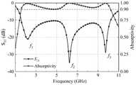
参阅图3,图3为本发明吸波结构在平面电磁波入射下的反射系数和吸收率。由结果可见,本发明提出的吸波结构能在较宽频带内实现电磁波的吸收效果,即在1.46GHz-10.27GHz内实现吸收率大于90%的吸波效果,相对带宽为150.2%。另外,我们也可以发现在这个宽吸收带内存在三个谐振点f1=2.19GHz,f2=6.24GHz,以及f3=9.74GHz,即本发明所提出的结构中存在多模谐振。参阅图4,图4为两个集总电阻在不同谐振频率下对入射的电磁波起到的吸收效果。可以发现,在谐振点f1时,集总电阻1和2吸收的能量相当,说明此时金属带1-1和1-2上的谐振都比较强。而当谐振频率为f2和f3时,集总电阻2吸收了大部分的能量,说明此时电流均从金属带1-2和集总电阻2上流过。Referring to Fig. 3, Fig. 3 shows the reflection coefficient and absorptivity of the wave-absorbing structure of the present invention under incident plane electromagnetic waves. It can be seen from the results that the absorbing structure proposed by the present invention can realize the absorption effect of electromagnetic waves in a wide frequency band, that is, the absorbing effect with an absorption rate greater than 90% can be realized within 1.46GHz-10.27GHz, and the relative bandwidth is 150.2%. In addition, we can also find that there are three resonance points f1 =2.19GHz, f2 =6.24GHz, and f3 =9.74GHz in this wide absorption band, that is, there are multi-mode resonances in the structure proposed by the present invention. Referring to FIG. 4, FIG. 4 shows the absorption effect of the two lumped resistors on the incident electromagnetic wave at different resonant frequencies. It can be found that at the resonance point f1, the energy absorbed by the lumped resistors1 and 2 is equivalent, indicating that the resonances on the metal strips 1-1 and 1-2 are relatively strong at this time. When the resonant frequency is f2 andf3 , the lumped resistor2 absorbs most of the energy, which means that the current flows through the metal strip 1-2 and the lumped
本发明与现有技术相比,其显著优点为:通过简易轻便的三维结构,构造了三个具有吸波功能的谐振模式,大大增加了吸波器的工作带宽,且结构本身的厚度仅为0.12个波长。另外,每个结构单元仅仅使用4个集总电阻和PCB加工工艺,大大降低了加工的难度和成本,有利于该吸波器在低可观测平台上的应用。Compared with the prior art, the present invention has the remarkable advantages that three resonant modes with absorbing functions are constructed through a simple and portable three-dimensional structure, which greatly increases the working bandwidth of the absorber, and the thickness of the structure itself is only 0.12 wavelengths. In addition, each structural unit only uses 4 lumped resistors and PCB processing technology, which greatly reduces the difficulty and cost of processing, and is conducive to the application of the absorber on low-observable platforms.
综上所述,以上仅为本发明的较佳实施例而已,并非用于限定本发明的保护范围。凡在本发明的精神和原则之内,所作的任何修改、等同替换、改进等,均应包含在本发明的保护范围之内。To sum up, the above are only preferred embodiments of the present invention, and are not intended to limit the protection scope of the present invention. Any modifications, equivalent replacements, improvements, etc. made within the spirit and principles of the present invention shall be included within the protection scope of the present invention.
Claims (4)
Translated fromChinesePriority Applications (1)
| Application Number | Priority Date | Filing Date | Title |
|---|---|---|---|
| CN202110975393.8ACN113794060B (en) | 2021-08-24 | 2021-08-24 | A dual-polarized ultra-broadband three-dimensional electromagnetic wave absorber |
Applications Claiming Priority (1)
| Application Number | Priority Date | Filing Date | Title |
|---|---|---|---|
| CN202110975393.8ACN113794060B (en) | 2021-08-24 | 2021-08-24 | A dual-polarized ultra-broadband three-dimensional electromagnetic wave absorber |
Publications (2)
| Publication Number | Publication Date |
|---|---|
| CN113794060A CN113794060A (en) | 2021-12-14 |
| CN113794060Btrue CN113794060B (en) | 2022-11-04 |
Family
ID=79182193
Family Applications (1)
| Application Number | Title | Priority Date | Filing Date |
|---|---|---|---|
| CN202110975393.8AActiveCN113794060B (en) | 2021-08-24 | 2021-08-24 | A dual-polarized ultra-broadband three-dimensional electromagnetic wave absorber |
Country Status (1)
| Country | Link |
|---|---|
| CN (1) | CN113794060B (en) |
Families Citing this family (1)
| Publication number | Priority date | Publication date | Assignee | Title |
|---|---|---|---|---|
| CN119181980B (en)* | 2024-11-01 | 2025-03-04 | 南京林业大学 | Low-profile dual-polarized electromagnetic metamaterial absorber with ultra-wideband wave absorbing characteristic |
Citations (8)
| Publication number | Priority date | Publication date | Assignee | Title |
|---|---|---|---|---|
| EP1383138A1 (en)* | 2002-07-18 | 2004-01-21 | Hokkaido University | Electromagnetic wave absorber |
| CN104411153A (en)* | 2014-12-15 | 2015-03-11 | 南京大学 | Polarized insensitive sub-wavelength three-dimensional wave absorption structure |
| CN105514619A (en)* | 2016-01-13 | 2016-04-20 | 武汉科技大学 | Ultra wideband material microwave absorber loaded with chip resistor |
| CN107799903A (en)* | 2017-10-12 | 2018-03-13 | 杭州电子科技大学 | Three-dimensional novel belt inhales molded breadth band frequency selecting structures |
| CN109818153A (en)* | 2019-02-28 | 2019-05-28 | 杭州电子科技大学 | A Novel Single-Polarized Three-Dimensional Ultra-Broadband Absorber |
| CN111342240A (en)* | 2019-12-21 | 2020-06-26 | 杭州电子科技大学 | Three-dimensional microwave absorber based on coupling gap structure and application thereof |
| CN112952400A (en)* | 2021-02-01 | 2021-06-11 | 西安电子科技大学 | Broadband wave-absorbing structure with high-transmittance wave-transmitting window |
| CN113131223A (en)* | 2021-04-02 | 2021-07-16 | 北京理工大学 | Electromagnetic wave absorber with dual polarization and double absorption bands |
Family Cites Families (1)
| Publication number | Priority date | Publication date | Assignee | Title |
|---|---|---|---|---|
| US10424847B2 (en)* | 2017-09-08 | 2019-09-24 | Raytheon Company | Wideband dual-polarized current loop antenna element |
- 2021
- 2021-08-24CNCN202110975393.8Apatent/CN113794060B/enactiveActive
Patent Citations (8)
| Publication number | Priority date | Publication date | Assignee | Title |
|---|---|---|---|---|
| EP1383138A1 (en)* | 2002-07-18 | 2004-01-21 | Hokkaido University | Electromagnetic wave absorber |
| CN104411153A (en)* | 2014-12-15 | 2015-03-11 | 南京大学 | Polarized insensitive sub-wavelength three-dimensional wave absorption structure |
| CN105514619A (en)* | 2016-01-13 | 2016-04-20 | 武汉科技大学 | Ultra wideband material microwave absorber loaded with chip resistor |
| CN107799903A (en)* | 2017-10-12 | 2018-03-13 | 杭州电子科技大学 | Three-dimensional novel belt inhales molded breadth band frequency selecting structures |
| CN109818153A (en)* | 2019-02-28 | 2019-05-28 | 杭州电子科技大学 | A Novel Single-Polarized Three-Dimensional Ultra-Broadband Absorber |
| CN111342240A (en)* | 2019-12-21 | 2020-06-26 | 杭州电子科技大学 | Three-dimensional microwave absorber based on coupling gap structure and application thereof |
| CN112952400A (en)* | 2021-02-01 | 2021-06-11 | 西安电子科技大学 | Broadband wave-absorbing structure with high-transmittance wave-transmitting window |
| CN113131223A (en)* | 2021-04-02 | 2021-07-16 | 北京理工大学 | Electromagnetic wave absorber with dual polarization and double absorption bands |
Non-Patent Citations (3)
| Title |
|---|
| 3-D Absorptive Frequency Selective Reflector for Antenna Radar Cross Section Reduction;Hao Huang等;《IEEE Transactions on Antennas and Propagation》;20170913;第65卷(第11期);全文* |
| Low-RCS and Wideband Reflectarray Antenna With High Radiation Efficiency;Binchao Zhang等;《IEEE Transactions on Antennas and Propagation》;IEEE;20201221;第69卷(第7期);第II、II部分,图1* |
| 三维吸收式频率选择反射与传输结构研究;刘璇;《中国优秀博硕士学位论文全文数据库(硕士)信息科技辑》;20210215;全文* |
Also Published As
| Publication number | Publication date |
|---|---|
| CN113794060A (en) | 2021-12-14 |
Similar Documents
| Publication | Publication Date | Title |
|---|---|---|
| CN103700951B (en) | Complex media double-deck FSS structure SRR metal level ultra-thin absorbing material | |
| CN106058482B (en) | Transparent wideband electromagnetic wave absorbing device based on bilayer conductive film | |
| CN106058483B (en) | The broadband absorbing material of stable polarization | |
| CN107257035B (en) | Six-frequency-band metamaterial wave absorber insensitive to microwave band polarization | |
| CN103490171A (en) | Composite wave-absorbing material with wide frequency bands | |
| CN112821081A (en) | Absorption and transmission integrated frequency selective surface with high-frequency broadband wave absorption and low-frequency wave transmission | |
| CN107508017A (en) | A kind of band inhales molded breadth band frequency selecting structures and its application | |
| CN114204279B (en) | Resistance loading quad ring ultra wide band absorbing structure | |
| CN109509987B (en) | Novel 2D/3D combined dual-polarized ultra-broadband absorbing structure | |
| CN108879109A (en) | The ultra wide band angle stabilization Salisbury for loading FSS inhales wave screen | |
| CN107799903A (en) | Three-dimensional novel belt inhales molded breadth band frequency selecting structures | |
| CN103682672A (en) | Frequency selective surface based ultrathin broadband wave-absorbing material | |
| CN107946761A (en) | A kind of iron-based wave-absorber based on bandpass-type frequency-selective surfaces | |
| CN110137691A (en) | Ultra wide band wave absorbing device based on periodical magnetic material | |
| CN110534908A (en) | A kind of Meta Materials transparent microwave absorber of composite stereo formula ultra-wide band | |
| CN114447622A (en) | Design of a broadband ultra-thin transparent wave absorber | |
| CN115296040A (en) | Resistance loading regular hexagonal ring ultra wide band wave absorbing structure | |
| CN116207516A (en) | A high-performance metamaterial absorber based on a three-layer metasurface | |
| CN113794060B (en) | A dual-polarized ultra-broadband three-dimensional electromagnetic wave absorber | |
| CN114843725B (en) | Ultra-wideband wide-angle band-stop type frequency selective surface | |
| CN116315730A (en) | A multi-layer high-performance ultra-broadband absorbing structure | |
| CN104767009A (en) | A waveguide integrated artificial surface plasmon device and a filter integrated waveguide substrate | |
| CN106785476B (en) | Metamaterial wave absorber | |
| CN207818905U (en) | A Novel Three-Dimensional Absorbing Broadband Frequency Selective Structure | |
| CN114597673A (en) | Electromagnetic metamaterial wave absorber based on broken line type resonance structure |
Legal Events
| Date | Code | Title | Description |
|---|---|---|---|
| PB01 | Publication | ||
| PB01 | Publication | ||
| SE01 | Entry into force of request for substantive examination | ||
| SE01 | Entry into force of request for substantive examination | ||
| GR01 | Patent grant | ||
| GR01 | Patent grant |