Movatterモバイル変換


[0]ホーム

URL:


CN113765349B - accelerated discharge device - Google Patents

accelerated discharge device
Download PDF

Info

Publication number
CN113765349B
CN113765349BCN202010488706.2ACN202010488706ACN113765349BCN 113765349 BCN113765349 BCN 113765349BCN 202010488706 ACN202010488706 ACN 202010488706ACN 113765349 BCN113765349 BCN 113765349B
Authority
CN
China
Prior art keywords
coupled
node
diode
terminal
potential
Prior art date
Legal status (The legal status is an assumption and is not a legal conclusion. Google has not performed a legal analysis and makes no representation as to the accuracy of the status listed.)
Active
Application number
CN202010488706.2A
Other languages
Chinese (zh)
Other versions
CN113765349A (en
Inventor
詹子增
Current Assignee (The listed assignees may be inaccurate. Google has not performed a legal analysis and makes no representation or warranty as to the accuracy of the list.)
Acer Inc
Original Assignee
Acer Inc
Priority date (The priority date is an assumption and is not a legal conclusion. Google has not performed a legal analysis and makes no representation as to the accuracy of the date listed.)
Filing date
Publication date
Application filed by Acer IncfiledCriticalAcer Inc
Priority to CN202010488706.2ApriorityCriticalpatent/CN113765349B/en
Publication of CN113765349ApublicationCriticalpatent/CN113765349A/en
Application grantedgrantedCritical
Publication of CN113765349BpublicationCriticalpatent/CN113765349B/en
Activelegal-statusCriticalCurrent
Anticipated expirationlegal-statusCritical

Links

Images

Classifications

Landscapes

Abstract

An accelerated discharge device comprising: a first parallel inductance element, a second parallel inductance element, a first capacitor, a noise suppression element, a unidirectional element, a first discharge circuit, a second discharge circuit, a first switch, and a second switch. The first parallel inductor element generates a first control potential according to a first input potential. The second parallel inductor generates a second control potential according to a second input potential. The first switch selectively couples the first parallel inductor element to ground through the second discharge circuit according to a first control potential. The second switch selectively couples the second parallel inductor element to the ground through the second discharging circuit according to a second control potential.

Description

Translated fromChinese
加速放电装置accelerated discharge device

技术领域technical field

本发明涉及一种加速放电装置,特别涉及一种可符合国际电工委员会的规范的加速放电装置。The invention relates to an accelerated discharge device, in particular to an accelerated discharge device that can meet the specifications of the International Electrotechnical Commission.

背景技术Background technique

国际电工委员会(International Electrotechnical Commission,IEC)已订定全新安全标准IEC 62368-1第二版,其将于2020年12月20日强制生效,并取代现行的IEC60950标准。The International Electrotechnical Commission (IEC) has formulated the second edition of the new safety standard IEC 62368-1, which will come into force on December 20, 2020 and replace the current IEC60950 standard.

根据IEC 62368-1第二版的规范,若在正常条件下将装置的外部输入电源移除,则装置的输入电位必须在2秒内放电至60V;反之,若在非正常条件下将装置的外部输入电源移除,则装置的输入电位须在2秒内放电至120V。然而,传统的电源供应器却往往无法达到前述规范。有鉴于此,势必要提出一种全新的解决方案,以克服现有技术所面临的缺陷。According to the specification of the second edition of IEC 62368-1, if the external input power of the device is removed under normal conditions, the input potential of the device must be discharged to 60V within 2 seconds; When the external input power is removed, the input potential of the device must be discharged to 120V within 2 seconds. However, conventional power supplies often fail to meet the aforementioned specifications. In view of this, it is necessary to propose a brand-new solution to overcome the defects faced by the prior art.

发明内容Contents of the invention

在优选实施例中,本发明提出一种加速放电装置,包括:一第一并联式电感元件,根据一第一输入电位来产生一第一控制电位;一第二并联式电感元件,根据一第二输入电位来产生一第二控制电位;一第一电容器,耦接于该第一并联式电感元件和该第二并联式电感元件之间;一噪声抑制元件,降低该第一并联式电感元件和该第二并联式电感元件之间的互相干扰;一单向元件,限制该第一控制电位和该第二控制电位于单一传递方向;一第一放电电路,耦接于该第一并联式电感元件和该第二并联式电感元件之间;一第二放电电路;一第一切换器,根据该第一控制电位来选择性地将该第一并联式电感元件经由该第二放电电路耦接至大地;以及一第二切换器,根据该第二控制电位来选择性地将该第二并联式电感元件经由该第二放电电路耦接至该大地。In a preferred embodiment, the present invention proposes an accelerated discharge device, comprising: a first parallel inductive element, which generates a first control potential according to a first input potential; a second parallel inductive element, which generates a first control potential according to a first Two input potentials are used to generate a second control potential; a first capacitor is coupled between the first parallel inductive element and the second parallel inductive element; a noise suppression element is used to reduce the first parallel inductive element and the mutual interference between the second parallel inductive element; a unidirectional element, which limits the first control potential and the second control potential to be in a single transmission direction; a first discharge circuit, coupled to the first parallel Between the inductance element and the second parallel inductance element; a second discharge circuit; a first switch, selectively coupling the first parallel inductance element through the second discharge circuit according to the first control potential connected to the ground; and a second switcher selectively coupling the second parallel inductive element to the ground through the second discharge circuit according to the second control potential.

附图说明Description of drawings

图1是显示根据本发明一实施例所述的加速放电装置的示意图。FIG. 1 is a schematic diagram showing an accelerated discharge device according to an embodiment of the present invention.

图2是显示根据本发明一实施例所述的加速放电装置的示意图。FIG. 2 is a schematic diagram showing an accelerated discharge device according to an embodiment of the present invention.

图3是显示根据本发明一实施例所述的断电测试模式中加速放电装置的第一输入电位的波形图。FIG. 3 is a waveform diagram showing a first input potential of the accelerating discharge device in the power-off test mode according to an embodiment of the present invention.

图4是显示根据本发明一实施例所述的断电测试模式中加速放电装置的第一输入电位的波形图。FIG. 4 is a waveform diagram showing a first input potential of the accelerating discharge device in the power-off test mode according to an embodiment of the present invention.

其中,附图标记说明如下:Wherein, the reference signs are explained as follows:

100,200:加速放电装置100, 200: accelerated discharge device

110,210:第一并联式电感元件110, 210: the first parallel inductance element

120,220:第二并联式电感元件120, 220: the second parallel inductance element

130,230:噪声抑制元件130, 230: noise suppression components

140,240:单向元件140, 240: Unidirectional elements

150,250:第一放电电路150, 250: the first discharge circuit

160,260:第一切换器160, 260: first switcher

170,270:第二切换器170, 270: second switcher

180,280:第二放电电路180, 280: the second discharge circuit

199,299:大地199, 299: Earth

290:桥式整流器290: Bridge Rectifier

C1:第一电容器C1: first capacitor

C2:第二电容器C2: second capacitor

D1:第一二极管D1: first diode

D2:第二二极管D2: second diode

D3:第三二极管D3: third diode

D4:第四二极管D4: fourth diode

D5:第五二极管D5: fifth diode

D6:第六二极管D6: sixth diode

D7:第七二极管D7: seventh diode

D8:第八二极管D8: eighth diode

L1:第一电感器L1: first inductor

L2:第二电感器L2: Second inductor

L3:第三电感器L3: Third inductor

L4:第四电感器L4: Fourth inductor

M1:第一晶体管M1: first transistor

M2:第二晶体管M2: second transistor

N1:第一节点N1: the first node

N2:第二节点N2: second node

N3:第三节点N3: the third node

N4:第四节点N4: the fourth node

N5:第五节点N5: fifth node

N6:第六节点N6: sixth node

N7:第七节点N7: seventh node

N8:第八节点N8: eighth node

N9:第九节点N9: ninth node

N10:第十节点N10: tenth node

NIN1:第一输入节点NIN1: first input node

NIN2:第二输入节点NIN2: second input node

R1:第一电阻器R1: first resistor

R2:第二电阻器R2: second resistor

R3:第三电阻器R3: third resistor

R4:第四电阻器R4: Fourth resistor

T1:第一放电时间T1: first discharge time

T2:第二放电时间T2: second discharge time

VIN1:第一输入电位VIN1: the first input potential

VIN2:第二输入电位VIN2: second input potential

VC1:第一控制电位VC1: first control potential

VC2:第二控制电位VC2: second control potential

VSS:接地电位VSS: ground potential

具体实施方式Detailed ways

为让本发明的目的、特征和优点能更明显易懂,下文特举出本发明的具体实施例,并配合附图,作详细说明如下。In order to make the purpose, features and advantages of the present invention more comprehensible, specific embodiments of the present invention are listed below and described in detail with accompanying drawings.

在说明书及权利要求当中使用了某些词汇来指称特定的元件。本领域技术人员应可理解,硬件制造商可能会用不同的名词来称呼同一个元件。本说明书及权利要求并不以名称的差异来作为区分元件的方式,而是以元件在功能上的差异来作为区分的准则。在通篇说明书及权利要求当中所提及的“包含”及“包括”一词为开放式的用语,故应解释成“包含但不仅限定于”。“大致”一词则是指在可接受的误差范围内,本领域技术人员能够在一定误差范围内解决所述技术问题,达到所述基本的技术效果。此外,“耦接”一词在本说明书中包含任何直接及间接的电性连接手段。因此,若文中描述一第一装置耦接至一第二装置,则代表该第一装置可直接电性连接至该第二装置,或经由其它装置或连接手段而间接地电性连接至该第二装置。Certain terms are used in the description and claims to refer to particular elements. Those skilled in the art should understand that hardware manufacturers may use different terms to refer to the same component. The specification and claims do not use the difference in name as a way to distinguish components, but use the difference in function of components as a criterion for distinguishing. The words "comprising" and "comprising" mentioned throughout the specification and claims are open-ended terms, so they should be interpreted as "including but not limited to". The term "approximately" means that within an acceptable error range, those skilled in the art can solve the technical problem within a certain error range and achieve the basic technical effect. In addition, the term "coupled" in this specification includes any direct and indirect electrical connection means. Therefore, if it is described that a first device is coupled to a second device, it means that the first device can be directly electrically connected to the second device, or indirectly electrically connected to the second device through other devices or connection means. Two devices.

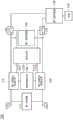
图1是显示根据本发明一实施例所述的加速放电装置100的示意图。例如,加速放电装置100可应用于一电源供应器,但亦不仅限于此。如图1所示,加速放电装置100包括:一第一电容器C1、一第一并联式电感元件110、一第二并联式电感元件120、一噪声抑制元件130、一单向元件140、一第一放电电路150、一第一切换器160、一第二切换器170,以及一第二放电电路180。必须注意的是,虽然未显示于图1中,但加速放电装置100还可包括其他元件,例如:一稳压器或(且)一负反馈电路。FIG. 1 is a schematic diagram showing anaccelerated discharge device 100 according to an embodiment of the present invention. For example, the accelerateddischarge device 100 can be applied to a power supply, but it is not limited thereto. As shown in Figure 1, the accelerateddischarge device 100 includes: a first capacitor C1, a firstparallel inductance element 110, a secondparallel inductance element 120, anoise suppression element 130, a unidirectional element 140, a first A discharge circuit 150 , afirst switch 160 , asecond switch 170 , and a second discharge circuit 180 . It should be noted that, although not shown in FIG. 1 , the accelerateddischarge device 100 may also include other components, such as a voltage regulator and/or a negative feedback circuit.

第一并联式电感元件110是根据一第一输入电位VIN1来产生一第一控制电位VC1。第二并联式电感元件120是根据一第二输入电位VIN2来产生一第二控制电位VC2。第一输入电位VIN1和第二输入电位VIN2皆可来自一外部输入电源,其中第一输入电位VIN1和第二输入电位VIN2之间可形成具有任意频率和任意振幅的一交流电压。例如,此交流电压的频率可约为50Hz或60Hz,而交流电压的方均根值可约由90V至264V,但亦不仅限于此。第一电容器C1是耦接于第一并联式电感元件110和第二并联式电感元件120之间。噪声抑制元件130是用于降低第一并联式电感元件110和第二并联式电感元件120之间的互相干扰。单向元件140是用于限制第一控制电位VC1和第二控制电位VC2于单一传递方向。第一放电电路150是耦接于第一并联式电感元件110和第二并联式电感元件120之间。第一切换器160是根据第一控制电位VC1来选择性地将第一并联式电感元件110经由第二放电电路180耦接至大地199。大地199可指地球,或指耦接至地球的任一接地路径,其并非属于加速放电装置100的内部元件。例如,若第一控制电位VC1为高逻辑电平(例如:逻辑“1”),则第一切换器160即将第一并联式电感元件110经由第二放电电路180耦接至大地199(亦即,第一切换器160可近似于一短路路径);反之,若第一控制电位VC1为低逻辑电平(例如:逻辑“0”),则第一切换器160不会将第一并联式电感元件110经由第二放电电路180耦接至大地199(亦即,第一切换器160可近似于一开路路径)。第二切换器170是根据第二控制电位VC2来选择性地将第二并联式电感元件120经由第二放电电路180耦接至大地199。例如,若第二控制电位VC2为高逻辑电平,则第二切换器170即将第二并联式电感元件120经由第二放电电路180耦接至大地199(亦即,第二切换器170可近似于一短路路径);反之,若第二控制电位VC2为低逻辑电平,则第二切换器170不会将第二并联式电感元件120经由第二放电电路180耦接至大地199(亦即,第二切换器170可近似于一开路路径)。根据实际测量结果,这种设计方式可在外部输入电源被移除时(或第一输入电位VIN1和第二输入电位VIN2皆消失时)大幅提升加速放电装置100的整体放电速度,以符合IEC 62368-1第二版的规范。The firstparallel inductance element 110 generates a first control potential VC1 according to a first input potential VIN1 . The second parallelinductive element 120 generates a second control potential VC2 according to a second input potential VIN2 . Both the first input potential VIN1 and the second input potential VIN2 can come from an external input power source, wherein an AC voltage with any frequency and any amplitude can be formed between the first input potential VIN1 and the second input potential VIN2 . For example, the frequency of the AC voltage can be about 50 Hz or 60 Hz, and the root mean square value of the AC voltage can be about 90V to 264V, but it is not limited thereto. The first capacitor C1 is coupled between the first parallelinductive element 110 and the second parallelinductive element 120 . Thenoise suppression element 130 is used to reduce the mutual interference between the first parallelinductive element 110 and the second parallelinductive element 120 . The one-way element 140 is used to limit the first control potential VC1 and the second control potential VC2 to a single transmission direction. The first discharge circuit 150 is coupled between the first parallelinductive element 110 and the second parallelinductive element 120 . Thefirst switch 160 selectively couples the first parallelinductive element 110 to the ground 199 via the second discharge circuit 180 according to the first control potential VC1 . The ground 199 may refer to the earth, or any ground path coupled to the earth, which is not an internal component of the accelerateddischarge device 100 . For example, if the first control potential VC1 is at a high logic level (for example: logic “1”), thefirst switch 160 is about to couple the first parallelinductive element 110 to the ground 199 via the second discharge circuit 180 (that is, , thefirst switch 160 can be approximated as a short-circuit path); on the contrary, if the first control potential VC1 is a low logic level (for example: logic "0"), thefirst switch 160 will not connect the first shunt inductor Theelement 110 is coupled to the ground 199 via the second discharge circuit 180 (ie, thefirst switch 160 can be approximated as an open path). Thesecond switch 170 selectively couples the second parallelinductive element 120 to the ground 199 via the second discharge circuit 180 according to the second control potential VC2 . For example, if the second control potential VC2 is a high logic level, thesecond switch 170 is about to couple the second parallelinductive element 120 to the ground 199 via the second discharge circuit 180 (that is, thesecond switch 170 can approximate on a short-circuit path); on the contrary, if the second control potential VC2 is a low logic level, thesecond switcher 170 will not couple the second parallelinductive element 120 to the ground 199 through the second discharge circuit 180 (that is, , thesecond switch 170 can be approximated as an open path). According to actual measurement results, this design method can greatly increase the overall discharge speed of the accelerateddischarge device 100 when the external input power is removed (or when both the first input potential VIN1 and the second input potential VIN2 disappear), so as to comply with IEC 62368 -1 for the second edition of the specification.

以下实施例将介绍加速放电装置100的详细结构及操作方式。必须理解的是,这些附图和叙述仅为举例,而非用于限制本发明的范围。The following embodiments will introduce the detailed structure and operation of the accelerateddischarge device 100 . It must be understood that these drawings and descriptions are only examples and not intended to limit the scope of the present invention.

图2是显示根据本发明一实施例所述的加速放电装置200的示意图。在图2的实施例中,加速放电装置200具有一第一输入节点NIN1和一第二输入节点NIN2,并包括一第一电容器C1、一第一并联式电感元件210、一第二并联式电感元件220、一噪声抑制元件230、一单向元件240、一第一放电电路250、一第一切换器260、一第二切换器270,以及一第二放电电路280。加速放电装置200的第一输入节点NIN1和第二输入节点NIN2可由一外部输入电源处分别接收一第一输入电位VIN1和一第二输入电位VIN2,其中第一输入电位VIN1和第二输入电位VIN2之间可形成具有任意频率和任意振幅的一交流电压。FIG. 2 is a schematic diagram showing anaccelerated discharge device 200 according to an embodiment of the present invention. In the embodiment of FIG. 2, the acceleratingdischarge device 200 has a first input node NIN1 and a second input node NIN2, and includes a first capacitor C1, a firstparallel inductance element 210, a second parallel inductance Theelement 220 , anoise suppression element 230 , a one-way element 240 , a first discharge circuit 250 , afirst switch 260 , asecond switch 270 , and asecond discharge circuit 280 . The first input node NIN1 and the second input node NIN2 of the acceleratingdischarge device 200 can respectively receive a first input potential VIN1 and a second input potential VIN2 from an external input power source, wherein the first input potential VIN1 and the second input potential VIN2 An alternating voltage with any frequency and any amplitude can be formed between them.

第一电容器C1的第一端是耦接至第一输入节点NIN1,而第一电容器C1的第二端是耦接至第二输入节点NIN2。A first terminal of the first capacitor C1 is coupled to the first input node NIN1 , and a second terminal of the first capacitor C1 is coupled to the second input node NIN2 .

第一并联式电感元件210包括一第一电感器L1和一第二电感器L2。第一电感器L1的第一端是耦接至第一输入节点NIN1,而第一电感器L1的第二端是耦接至一第一节点N1以输出一第一控制电位VC1。第二电感器L2的第一端是耦接至第一输入节点NIN1,而第二电感器L2的第二端是耦接至第一节点N1。The firstparallel inductance element 210 includes a first inductor L1 and a second inductor L2. A first terminal of the first inductor L1 is coupled to the first input node NIN1 , and a second terminal of the first inductor L1 is coupled to a first node N1 to output a first control potential VC1 . A first terminal of the second inductor L2 is coupled to the first input node NIN1 , and a second terminal of the second inductor L2 is coupled to the first node N1 .

第二并联式电感元件220包括一第三电感器L3和一第四电感器L4。第三电感器L3的第一端是耦接至第二输入节点NIN2,而第三电感器L3的第二端是耦接至一第二节点N2以输出一第二控制电位VC2。第四电感器L4的第一端是耦接至第二输入节点NIN2,而第四电感器L4的第二端是耦接至第二节点N2。在一些实施例中,第三电感器L3是与第二电感器L2形成于同一铁芯上,使得第三电感器L3和第二电感器L2两者互相耦合。The secondparallel inductance element 220 includes a third inductor L3 and a fourth inductor L4. A first terminal of the third inductor L3 is coupled to the second input node NIN2, and a second terminal of the third inductor L3 is coupled to a second node N2 to output a second control potential VC2. A first terminal of the fourth inductor L4 is coupled to the second input node NIN2, and a second terminal of the fourth inductor L4 is coupled to the second node N2. In some embodiments, the third inductor L3 is formed on the same core as the second inductor L2, so that the third inductor L3 and the second inductor L2 are coupled to each other.

噪声抑制元件230包括一第一二极管D1和一第二二极管D2。第一二极管D1的阳极是耦接至第一输入节点NIN1,而第一二极管D1的阴极是耦接至一第三节点N3。第二二极管D2的阳极是耦接至第二输入节点NIN2,而第二二极管D2的阴极是耦接至第三节点N3。在一些实施例中,噪声抑制元件230可用于防止电压噪声或电流噪声于第二电感器L2和第三电感器L3之间进行传递,即使此二者是形成于同一铁芯上。Thenoise suppression element 230 includes a first diode D1 and a second diode D2. The anode of the first diode D1 is coupled to the first input node NIN1, and the cathode of the first diode D1 is coupled to a third node N3. The anode of the second diode D2 is coupled to the second input node NIN2, and the cathode of the second diode D2 is coupled to the third node N3. In some embodiments, thenoise suppression element 230 can be used to prevent voltage noise or current noise from being transferred between the second inductor L2 and the third inductor L3 even though they are formed on the same core.

单向元件240包括一第三二极管D3和一第四二极管D4。第三二极管D3的阳极是耦接至第一节点N1以接收第一控制电位VC1,而第三二极管D3的阴极是耦接至一第四节点N4。第四二极管D4的阳极是耦接至第二节点N2以接收第二控制电位VC2,而第四二极管D4的阴极是耦接至一第五节点N5。在一些实施例中,第三二极管D3可限制第一控制电位VC1仅能由第一节点N1传送往第四节点N4,而第四二极管D4可限制第二控制电位VC2仅能由第二节点N2传送往第五节点N5。亦即,单向元件240可避免第一控制电位VC1和第二控制电位VC2意外回灌至第一并联式电感元件210和第二并联式电感元件220。The one-way element 240 includes a third diode D3 and a fourth diode D4. The anode of the third diode D3 is coupled to the first node N1 to receive the first control potential VC1, and the cathode of the third diode D3 is coupled to a fourth node N4. The anode of the fourth diode D4 is coupled to the second node N2 to receive the second control potential VC2, and the cathode of the fourth diode D4 is coupled to a fifth node N5. In some embodiments, the third diode D3 can limit the first control potential VC1 to only be transmitted from the first node N1 to the fourth node N4, and the fourth diode D4 can limit the second control potential VC2 to only be transmitted from the first node N1 to the fourth node N4. The second node N2 transmits to the fifth node N5. That is, theunidirectional element 240 can prevent the first control potential VC1 and the second control potential VC2 from accidentally feeding back into the first parallelinductive element 210 and the second parallelinductive element 220 .

第一放电电路250包括一第一电阻器R1和一第二电阻器R2。第一电阻器R1的第一端是耦接至第一节点N1,而第一电阻器R1的第二端是耦接至一第六节点N6。第二电阻器R2的第一端是耦接至第二节点N2,而第二电阻器R2的第二端是耦接至第六节点N6。The first discharge circuit 250 includes a first resistor R1 and a second resistor R2. A first end of the first resistor R1 is coupled to the first node N1, and a second end of the first resistor R1 is coupled to a sixth node N6. A first end of the second resistor R2 is coupled to the second node N2, and a second end of the second resistor R2 is coupled to the sixth node N6.

第一切换器260包括一第一晶体管M1。第一晶体管M1可为一N型金属氧化物半导体场效晶体管。第一晶体管M1的控制端是耦接至第四节点N4(可间接地接收第一控制电位VC1),第一晶体管M1的第一端是耦接至一第七节点N7,而第一晶体管M1的第二端是耦接至第一节点N1。在一些实施例中,若第一控制电位VC1为高逻辑电平,则第一晶体管M1即被使能;反之,若第一控制电位VC1为低逻辑电平,则第一晶体管M1即被禁能。Thefirst switch 260 includes a first transistor M1. The first transistor M1 can be an NMOS field effect transistor. The control terminal of the first transistor M1 is coupled to the fourth node N4 (which can indirectly receive the first control potential VC1), the first terminal of the first transistor M1 is coupled to a seventh node N7, and the first transistor M1 The second terminal of is coupled to the first node N1. In some embodiments, if the first control potential VC1 is a high logic level, the first transistor M1 is enabled; otherwise, if the first control potential VC1 is a low logic level, the first transistor M1 is disabled. able.

第二切换器270包括一第二晶体管M2。第二晶体管M2可为一N型金属氧化物半导体场效晶体管。第二晶体管M2的控制端是耦接至第五节点N5(可间接地接收第二控制电位VC2),第二晶体管M2的第一端是耦接至一第八节点N8,而第二晶体管M2的第二端是耦接至第二节点N2。在一些实施例中,若第二控制电位VC2为高逻辑电平,则第二晶体管M2即被使能;反之,若第二控制电位VC2为低逻辑电平,则第二晶体管M2即被禁能。Thesecond switch 270 includes a second transistor M2. The second transistor M2 can be an NMOS field effect transistor. The control terminal of the second transistor M2 is coupled to the fifth node N5 (which can indirectly receive the second control potential VC2), the first terminal of the second transistor M2 is coupled to an eighth node N8, and the second transistor M2 The second terminal of is coupled to the second node N2. In some embodiments, if the second control potential VC2 is a high logic level, the second transistor M2 is enabled; otherwise, if the second control potential VC2 is a low logic level, the second transistor M2 is disabled. able.

第二放电电路280包括一第二电容器C2、一第三电阻器R3,以及一第四电阻器R4。第二电容器C2的第一端是耦接至第七节点N7,而第二电容器C2的第二端是耦接至第八节点N8。第三电阻器R3的第一端是耦接至第七节点N7,而第三电阻器R3的第二端是耦接至一第九节点N9。第九节点N9还可耦接至大地299。大地299可指地球,或指耦接至地球的任一接地路径,其并非属于加速放电装置200的内部元件。第四电阻器R4的第一端是耦接至第八节点N8,而第四电阻器R4的第二端是耦接至第九节点N9。Thesecond discharge circuit 280 includes a second capacitor C2, a third resistor R3, and a fourth resistor R4. A first terminal of the second capacitor C2 is coupled to the seventh node N7, and a second terminal of the second capacitor C2 is coupled to the eighth node N8. A first end of the third resistor R3 is coupled to the seventh node N7, and a second end of the third resistor R3 is coupled to a ninth node N9. The ninth node N9 can also be coupled to theground 299 . Theground 299 may refer to the earth, or any ground path coupled to the earth, which is not an internal component of the accelerateddischarge device 200 . A first end of the fourth resistor R4 is coupled to the eighth node N8, and a second end of the fourth resistor R4 is coupled to the ninth node N9.

在一些实施例中,加速放电装置200还包括一桥式整流器290。桥式整流器290包括一第五二极管D5、一第六二极管D6、一第七二极管D7,以及一第八二极管D8。第五二极管D5的阳极是耦接至一接地电位VSS(例如:0V),而第五二极管D5的阴极是耦接至第一节点N1。第六二极管D6的阳极是耦接至接地电位VSS,而第六二极管D6的阴极是耦接至第二节点N2。第七二极管D7的阳极是耦接至第一节点N1,而第七二极管D7的阴极是耦接至一第十节点N10。第八二极管D8的阳极是耦接至第二节点N2,而第八二极管D8的阴极是耦接至第十节点N10。必须注意的是,桥式整流器290仅为一选用元件,在其他实施例中亦可由加速放电装置200中移除。另外,若省略桥式整流器290,则第一节点N1或(且)第二节点N2亦可直接或间接地耦接至接地电位VSS。In some embodiments, the acceleratingdischarge device 200 further includes abridge rectifier 290 . Thebridge rectifier 290 includes a fifth diode D5, a sixth diode D6, a seventh diode D7, and an eighth diode D8. The anode of the fifth diode D5 is coupled to a ground potential VSS (for example: 0V), and the cathode of the fifth diode D5 is coupled to the first node N1. The anode of the sixth diode D6 is coupled to the ground potential VSS, and the cathode of the sixth diode D6 is coupled to the second node N2. The anode of the seventh diode D7 is coupled to the first node N1, and the cathode of the seventh diode D7 is coupled to a tenth node N10. The anode of the eighth diode D8 is coupled to the second node N2, and the cathode of the eighth diode D8 is coupled to the tenth node N10. It should be noted that thebridge rectifier 290 is only an optional component, and can also be removed from the acceleratingdischarge device 200 in other embodiments. In addition, if thebridge rectifier 290 is omitted, the first node N1 and/or the second node N2 may also be directly or indirectly coupled to the ground potential VSS.

在一些实施例中,加速放电装置200的操作原理可如下列所述。在一初始模式中,加速放电装置200尚未接收到第一输入电位VIN1和第二输入电位VIN2,故第一晶体管M1和第二晶体管M2均为禁能状态。在一正常操作模式中,加速放电装置200已接收到第一输入电位VIN1和第二输入电位VIN2,故第一电容器C1会开始存储能量,第一并联式电感元件210和第二并联式电感元件220会各自形成一电流路径,而第一晶体管M1和第二晶体管M2则会轮流被使能。详细而言,若第一输入电位VIN1为正值(亦即,高于接地电位VSS),则第一电容器C1上一部分的能量将会经由第一放电电路250释放至接地电位VSS,而第一电容器C1上另一部分的能量将会经由使能的第一晶体管M1和第二放电电路280释放至大地299。反之,若第二输入电位VIN2为正值,则第一电容器C1上一部分的能量将会经由第一放电电路250释放至接地电位VSS,而第一电容器C1上另一部分的能量将会经由使能的第二晶体管M2和第二放电电路280释放至大地299。在一断电测试模式中,对应的外部输入电源会被移除(或是第一输入电位VIN1和第二输入电位VIN2皆消失),此时第一电容器C1所存储的能量仍可通过前述的放电路径进行释放。必须注意的是,由于同时使用第一并联式电感元件210、第二并联式电感元件220、第一放电电路250,以及第二放电电路280,故加速放电装置200的整体放电时间将能大幅缩短。In some embodiments, the operation principle of the accelerateddischarge device 200 may be as follows. In an initial mode, the acceleratingdischarge device 200 has not received the first input potential VIN1 and the second input potential VIN2, so both the first transistor M1 and the second transistor M2 are disabled. In a normal operation mode, the accelerateddischarge device 200 has received the first input potential VIN1 and the second input potential VIN2, so the first capacitor C1 will start to store energy, and the first parallelinductive element 210 and the second parallelinductive element 220 will each form a current path, and the first transistor M1 and the second transistor M2 will be enabled in turn. In detail, if the first input potential VIN1 is positive (that is, higher than the ground potential VSS), a part of the energy on the first capacitor C1 will be discharged to the ground potential VSS through the first discharge circuit 250, and the first Another part of the energy on the capacitor C1 will be released to theground 299 via the enabled first transistor M1 and thesecond discharge circuit 280 . Conversely, if the second input potential VIN2 is a positive value, a part of the energy on the first capacitor C1 will be released to the ground potential VSS through the first discharge circuit 250, and another part of the energy on the first capacitor C1 will be released through the enable The second transistor M2 and thesecond discharge circuit 280 discharge to theground 299 . In a power-off test mode, the corresponding external input power will be removed (or both the first input potential VIN1 and the second input potential VIN2 will disappear), at this time, the energy stored in the first capacitor C1 can still pass through the aforementioned discharge path for release. It must be noted that since the firstparallel inductance element 210, the secondparallel inductance element 220, the first discharge circuit 250, and thesecond discharge circuit 280 are used at the same time, the overall discharge time of the accelerateddischarge device 200 can be greatly shortened. .

图3是显示根据本发明一实施例所述的断电测试模式中加速放电装置200的第一输入电位VIN1的波形图。若在正常条件下将外部输入电源移除,则第一输入电位VIN1(或第二输入电位VIN2)由一高电位电平(例如:交流电压264V,或是直流电压370V)下降至60V所花费的一第一放电时间T1约为1.315秒,其小于IEC 62368-1第二版所规范的2秒。FIG. 3 is a waveform diagram showing the first input potential VIN1 of the acceleratingdischarge device 200 in the power-off test mode according to an embodiment of the present invention. If the external input power is removed under normal conditions, it takes the first input potential VIN1 (or the second input potential VIN2) to drop from a high potential level (for example: AC voltage 264V, or DC voltage 370V) to 60V A first discharge time T1 is about 1.315 seconds, which is less than 2 seconds specified in the second edition of IEC 62368-1.

图4是显示根据本发明一实施例所述的断电测试模式中加速放电装置200的第一输入电位VIN1的波形图。若在非正常条件下(亦即,加速放电装置200的任一元件被设定为开路或短路)将外部输入电源移除,则第一输入电位VIN1(或第二输入电位VIN2)由一高电位电平(例如:交流电压264V,或是直流电压370V)下降至120V所花费的一第二放电时间T2约为0.79秒,其亦小于IEC 62368-1第二版所规范的2秒。FIG. 4 is a waveform diagram showing the first input potential VIN1 of the acceleratingdischarge device 200 in the power-off test mode according to an embodiment of the present invention. If the external input power is removed under abnormal conditions (that is, any element of the accelerateddischarge device 200 is set to open or short circuit), the first input potential VIN1 (or the second input potential VIN2) will change from a high A second discharge time T2 taken for the potential level (for example: AC voltage 264V or DC voltage 370V) to drop to 120V is about 0.79 seconds, which is also less than 2 seconds specified in the second edition of IEC 62368-1.

在一些实施例中,加速放电装置200的元件参数可如下列所述。第一电容器C1的电容值可介于0.327μF至0.333μF之间,优选为0.33μF。第二电容器C2的电容值可介于0.99μF至1.01μF之间,优选为1μF。第一电感器L1的电感值可介于6.31mH至6.97mH之间,优选为6.64mH。第二电感器L2的电感值可介于6.31mH至6.97mH之间,优选为6.64mH。第三电感器L3的电感值可介于6.31mH至6.97mH之间,优选为6.64mH。第四电感器L4的电感值可介于6.31mH至6.97mH之间,优选为6.64mH。第一电阻器R1的电阻值可介于1.317MΩ至1.343MΩ之间,优选为1.33MΩ。第二电阻器R2的电阻值可介于1.317MΩ至1.343MΩ之间,优选为1.33MΩ。第三电阻器R3的电阻值可介于198KΩ至202KΩ之间,优选为200KΩ。第四电阻器R4的电阻值可介于198KΩ至202KΩ之间,优选为200KΩ。以上参数范围是根据多次实验结果而得出,其有助于最小化加速放电装置200的整体放电时间。In some embodiments, the component parameters of the acceleratingdischarge device 200 may be as follows. The capacitance of the first capacitor C1 can range from 0.327 μF to 0.333 μF, preferably 0.33 μF. The capacitance of the second capacitor C2 can range from 0.99 μF to 1.01 μF, preferably 1 μF. The inductance of the first inductor L1 can be between 6.31mH and 6.97mH, preferably 6.64mH. The inductance of the second inductor L2 can be between 6.31mH and 6.97mH, preferably 6.64mH. The inductance of the third inductor L3 can be between 6.31mH and 6.97mH, preferably 6.64mH. The inductance of the fourth inductor L4 can be between 6.31mH and 6.97mH, preferably 6.64mH. The resistance value of the first resistor R1 can be between 1.317MΩ and 1.343MΩ, preferably 1.33MΩ. The resistance value of the second resistor R2 can be between 1.317MΩ and 1.343MΩ, preferably 1.33MΩ. The resistance value of the third resistor R3 can be between 198KΩ and 202KΩ, preferably 200KΩ. The resistance value of the fourth resistor R4 can be between 198KΩ and 202KΩ, preferably 200KΩ. The above parameter ranges are obtained according to the results of multiple experiments, which help to minimize the overall discharge time of the accelerateddischarge device 200 .

本发明提出一种新颖的加速放电装置,其包括并联式电感元件和双重放电电路的设计。根据实际测量结果,使用前述设计的加速放电装置可大幅缩短其整体放电时间,且无论在正常条件或非正常条件下均能符合IEC 62368-1第二版的规范,故其很适合应用于各种各式的电子装置当中。The present invention proposes a novel accelerated discharge device, which includes a parallel inductance element and a double discharge circuit design. According to the actual measurement results, using the accelerated discharge device designed above can greatly shorten its overall discharge time, and it can meet the specifications of the second edition of IEC 62368-1 under normal or abnormal conditions, so it is very suitable for various applications. various electronic devices.

值得注意的是,以上所述的电位、电流、电阻值、电感值、电容值,以及其余元件参数均非为本发明的限制条件。设计者可以根据不同需要调整这些设定值。本发明的加速放电装置并不仅限于第1-4图所图示的状态。本发明可以仅包括图1-图4的任何一或多个实施例的任何一或多项特征。换言的,并非所有图示的特征均须同时实施于本发明的加速放电装置当中。虽然本发明的实施例是使用金属氧化物半导体场效晶体管为例,但本发明并不仅限于此,本技术领域人士可改用其他种类的晶体管,例如:接面场效晶体管,或是鳍式场效晶体管等等,而不致于影响本发明的效果。It should be noted that the potential, current, resistance value, inductance value, capacitance value, and other component parameters mentioned above are not limiting conditions of the present invention. Designers can adjust these settings according to different needs. The accelerated discharge device of the present invention is not limited to the states shown in FIGS. 1-4. The present invention may only include any one or more features of any one or more of the embodiments of FIGS. 1-4 . In other words, not all the illustrated features must be implemented in the accelerated discharge device of the present invention at the same time. Although the embodiment of the present invention uses metal-oxide-semiconductor field-effect transistors as an example, the present invention is not limited thereto, and those skilled in the art can use other types of transistors, such as: junction field-effect transistors, or fin-type field effect transistors, etc., without affecting the effect of the present invention.

在本说明书以及权利要求中的序数,例如“第一”、“第二”、“第三”等等,彼此之间并没有顺序上的先后关系,其仅用于标示区分两个具有相同名字的不同元件。The ordinal numbers in this specification and claims, such as "first", "second", "third", etc., have no sequential relationship with each other, and are only used to mark and distinguish two terms with the same name. of different components.

本发明虽以优选实施例公开如上,然其并非用以限定本发明的范围,任何熟习此项技艺者,在不脱离本发明的精神和范围内,当可做些许的变动与润饰,因此本发明的保护范围当视后附的权利要求所界定者为准。Although the present invention is disclosed as above with preferred embodiments, it is not intended to limit the scope of the present invention. Anyone skilled in this art can make some changes and modifications without departing from the spirit and scope of the present invention. Therefore, this The scope of protection of the invention shall prevail as defined by the appended claims.

Claims (10)

Translated fromChinese
1.一种加速放电装置,包括:1. An accelerated discharge device, comprising:一第一并联式电感元件,根据一第一输入电位来产生一第一控制电位;a first parallel inductance element, generating a first control potential according to a first input potential;一第二并联式电感元件,根据一第二输入电位来产生一第二控制电位;a second parallel inductance element, generating a second control potential according to a second input potential;一第一电容器,耦接于该第一并联式电感元件和该第二并联式电感元件之间;a first capacitor coupled between the first parallel inductive element and the second parallel inductive element;一噪声抑制元件,降低该第一并联式电感元件和该第二并联式电感元件之间的互相干扰;A noise suppression element, reducing the mutual interference between the first parallel inductive element and the second parallel inductive element;一单向元件,限制该第一控制电位和该第二控制电位于单一传递方向;a unidirectional element restricting the first control potential and the second control potential to a single transfer direction;一第一放电电路,耦接于该第一并联式电感元件和该第二并联式电感元件之间;a first discharge circuit, coupled between the first parallel inductive element and the second parallel inductive element;一第二放电电路;a second discharge circuit;一第一切换器,根据该第一控制电位来选择性地将该第一并联式电感元件经由该第二放电电路耦接至大地;以及a first switch selectively couples the first parallel inductive element to the ground through the second discharge circuit according to the first control potential; and一第二切换器,根据该第二控制电位来选择性地将该第二并联式电感元件经由该第二放电电路耦接至该大地。A second switch selectively couples the second parallel inductive element to the ground through the second discharge circuit according to the second control potential.2.如权利要求1所述的加速放电装置,其中该第一并联式电感元件包括:2. The device for accelerating discharge as claimed in claim 1, wherein the first parallel inductive element comprises:一第一电感器,具有一第一端和一第二端,其中该第一电感器的该第一端是耦接至一第一输入节点以接收该第一输入电位,而该第一电感器的该第二端是耦接至一第一节点以输出该第一控制电位;以及a first inductor having a first end and a second end, wherein the first end of the first inductor is coupled to a first input node to receive the first input potential, and the first inductor The second end of the device is coupled to a first node to output the first control potential; and一第二电感器,具有一第一端和一第二端,其中该第二电感器的该第一端是耦接至该第一输入节点,而该第二电感器的该第二端是耦接至该第一节点。a second inductor having a first end and a second end, wherein the first end of the second inductor is coupled to the first input node, and the second end of the second inductor is coupled to the first node.3.如权利要求2所述的加速放电装置,其中该第二并联式电感元件包括:3. The device for accelerating discharge as claimed in claim 2, wherein the second parallel inductive element comprises:一第三电感器,具有一第一端和一第二端,其中该第三电感器的该第一端是耦接至一第二输入节点以接收该第二输入电位,而该第三电感器的该第二端是耦接至一第二节点以输出该第二控制电位;以及a third inductor having a first end and a second end, wherein the first end of the third inductor is coupled to a second input node to receive the second input potential, and the third inductor The second terminal of the device is coupled to a second node to output the second control potential; and一第四电感器,具有一第一端和一第二端,其中该第四电感器的该第一端是耦接至该第二输入节点,而该第四电感器的该第二端是耦接至该第二节点;a fourth inductor having a first end and a second end, wherein the first end of the fourth inductor is coupled to the second input node, and the second end of the fourth inductor is coupled to the second node;其中该第一电容器具有一第一端和一第二端,该第一电容器的该第一端是耦接至该第一输入节点,而该第一电容器的该第二端是耦接至该第二输入节点。Wherein the first capacitor has a first terminal and a second terminal, the first terminal of the first capacitor is coupled to the first input node, and the second terminal of the first capacitor is coupled to the The second input node.4.如权利要求3所述的加速放电装置,其中该噪声抑制元件包括:4. The accelerating discharge device as claimed in claim 3, wherein the noise suppression element comprises:一第一二极管,具有一阳极和一阴极,其中该第一二极管的该阳极是耦接至该第一输入节点,而该第一二极管的该阴极是耦接至一第三节点;以及A first diode having an anode and a cathode, wherein the anode of the first diode is coupled to the first input node, and the cathode of the first diode is coupled to a first three nodes; and一第二二极管,具有一阳极和一阴极,其中该第二二极管的该阳极是耦接至该第二输入节点,而该第二二极管的该阴极是耦接至该第三节点。a second diode having an anode and a cathode, wherein the anode of the second diode is coupled to the second input node, and the cathode of the second diode is coupled to the first Three nodes.5.如权利要求3所述的加速放电装置,其中该单向元件包括:5. The accelerated discharge device as claimed in claim 3, wherein the one-way element comprises:一第三二极管,具有一阳极和一阴极,其中该第三二极管的该阳极是耦接至该第一节点以接收该第一控制电位,而该第三二极管的该阴极是耦接至一第四节点;以及a third diode having an anode and a cathode, wherein the anode of the third diode is coupled to the first node to receive the first control potential, and the cathode of the third diode is coupled to a fourth node; and一第四二极管,具有一阳极和一阴极,其中该第四二极管的该阳极是耦接至该第二节点以接收该第二控制电位,而该第四二极管的该阴极是耦接至一第五节点。a fourth diode having an anode and a cathode, wherein the anode of the fourth diode is coupled to the second node to receive the second control potential, and the cathode of the fourth diode is coupled to a fifth node.6.如权利要求3所述的加速放电装置,其中该第一放电电路包括:6. The device for accelerating discharge as claimed in claim 3, wherein the first discharge circuit comprises:一第一电阻器,具有一第一端和一第二端,其中该第一电阻器的该第一端是耦接至该第一节点,而该第一电阻器的该第二端是耦接至一第六节点;以及A first resistor having a first end and a second end, wherein the first end of the first resistor is coupled to the first node, and the second end of the first resistor is coupled to connected to a sixth node; and一第二电阻器,具有一第一端和一第二端,其中该第二电阻器的该第一端是耦接至该第二节点,而该第二电阻器的该第二端是耦接至该第六节点。A second resistor has a first end and a second end, wherein the first end of the second resistor is coupled to the second node, and the second end of the second resistor is coupled to connected to the sixth node.7.如权利要求5所述的加速放电装置,其中该第一切换器包括:7. The accelerating discharge device as claimed in claim 5, wherein the first switch comprises:一第一晶体管,具有一控制端、一第一端,以及一第二端,其中该第一晶体管的该控制端是耦接至该第四节点,该第一晶体管的该第一端是耦接至一第七节点,而该第一晶体管的该第二端是耦接至该第一节点。A first transistor has a control terminal, a first terminal, and a second terminal, wherein the control terminal of the first transistor is coupled to the fourth node, and the first terminal of the first transistor is coupled to connected to a seventh node, and the second terminal of the first transistor is coupled to the first node.8.如权利要求7所述的加速放电装置,其中该第二切换器包括:8. The accelerated discharge device as claimed in claim 7, wherein the second switch comprises:一第二晶体管,具有一控制端、一第一端,以及一第二端,其中该第二晶体管的该控制端是耦接至该第五节点,该第二晶体管的该第一端是耦接至一第八节点,而该第二晶体管的该第二端是耦接至该第二节点。A second transistor has a control terminal, a first terminal, and a second terminal, wherein the control terminal of the second transistor is coupled to the fifth node, and the first terminal of the second transistor is coupled to connected to an eighth node, and the second terminal of the second transistor is coupled to the second node.9.如权利要求8所述的加速放电装置,其中该第二放电电路包括:9. The device for accelerating discharge as claimed in claim 8, wherein the second discharge circuit comprises:一第二电容器,具有一第一端和一第二端,其中该第二电容器的该第一端是耦接至该第七节点,而该第二电容器的该第二端是耦接至该第八节点;A second capacitor having a first terminal and a second terminal, wherein the first terminal of the second capacitor is coupled to the seventh node, and the second terminal of the second capacitor is coupled to the eighth node;一第三电阻器,具有一第一端和一第二端,其中该第三电阻器的该第一端是耦接至该第七节点,而该第三电阻器的该第二端是耦接至一第九节点;以及A third resistor has a first end and a second end, wherein the first end of the third resistor is coupled to the seventh node, and the second end of the third resistor is coupled to connected to a ninth node; and一第四电阻器,具有一第一端和一第二端,其中该第四电阻器的该第一端是耦接至该第八节点,而该第四电阻器的该第二端是耦接至该第九节点;A fourth resistor has a first end and a second end, wherein the first end of the fourth resistor is coupled to the eighth node, and the second end of the fourth resistor is coupled to connected to the ninth node;其中该第九节点更耦接至该大地。Wherein the ninth node is further coupled to the ground.10.如权利要求3所述的加速放电装置,还包括一桥式整流器,其中该桥式整流器包括:10. The accelerating discharge device as claimed in claim 3, further comprising a bridge rectifier, wherein the bridge rectifier comprises:一第五二极管,具有一阳极和一阴极,其中该第五二极管的该阳极是耦接至一接地电位,而该第五二极管的该阴极是耦接至该第一节点;a fifth diode having an anode and a cathode, wherein the anode of the fifth diode is coupled to a ground potential and the cathode of the fifth diode is coupled to the first node ;一第六二极管,具有一阳极和一阴极,其中该第六二极管的该阳极是耦接至该接地电位,而该第六二极管的该阴极是耦接至该第二节点;a sixth diode having an anode and a cathode, wherein the anode of the sixth diode is coupled to the ground potential and the cathode of the sixth diode is coupled to the second node ;一第七二极管,具有一阳极和一阴极,其中该第七二极管的该阳极是耦接至该第一节点,而该第七二极管的该阴极是耦接至一第十节点;以及A seventh diode having an anode and a cathode, wherein the anode of the seventh diode is coupled to the first node, and the cathode of the seventh diode is coupled to a tenth node; and一第八二极管,具有一阳极和一阴极,其中该第八二极管的该阳极是耦接至该第二节点,而该第八二极管的该阴极是耦接至该第十节点。An eighth diode having an anode and a cathode, wherein the anode of the eighth diode is coupled to the second node, and the cathode of the eighth diode is coupled to the tenth node.
CN202010488706.2A2020-06-022020-06-02 accelerated discharge deviceActiveCN113765349B (en)

Priority Applications (1)

Application NumberPriority DateFiling DateTitle
CN202010488706.2ACN113765349B (en)2020-06-022020-06-02 accelerated discharge device

Applications Claiming Priority (1)

Application NumberPriority DateFiling DateTitle
CN202010488706.2ACN113765349B (en)2020-06-022020-06-02 accelerated discharge device

Publications (2)

Publication NumberPublication Date
CN113765349A CN113765349A (en)2021-12-07
CN113765349Btrue CN113765349B (en)2023-05-09

Family

ID=78782736

Family Applications (1)

Application NumberTitlePriority DateFiling Date
CN202010488706.2AActiveCN113765349B (en)2020-06-022020-06-02 accelerated discharge device

Country Status (1)

CountryLink
CN (1)CN113765349B (en)

Citations (5)

* Cited by examiner, † Cited by third party
Publication numberPriority datePublication dateAssigneeTitle
EP0872004A1 (en)*1995-06-051998-10-21Powervar, Inc.Transformerless conditioning of a power distribution system
TW201023509A (en)*2008-12-112010-06-16Ind Tech Res InstESD clamp circuit applied to power amplifier
CN201966817U (en)*2010-11-192011-09-07Tcl王牌电器(惠州)有限公司Alternating current voltage sampling and shutdown capacitor discharging circuit
TW201138253A (en)*2010-04-222011-11-01Leadtrend Tech CorpDischarging module applied in a switched-mode power supply and method thereof
CN108933519A (en)*2017-05-222018-12-04伟诠电子股份有限公司Control circuit and method for detecting power receiving state and discharging capacitor voltage according to the detected state

Family Cites Families (3)

* Cited by examiner, † Cited by third party
Publication numberPriority datePublication dateAssigneeTitle
US8450988B2 (en)*2010-10-052013-05-28Maxim Integrated Products, Inc.Systems and methods for controlling inductive energy in DC-DC converters
TWI479764B (en)*2012-12-172015-04-01Niko Semiconductor Co LtdLow power bleeder circuit and ac converter having the same
TWI511433B (en)*2013-12-202015-12-01Niko Semiconductor Co LtdPower conversion apparatus and control chip thereof

Patent Citations (5)

* Cited by examiner, † Cited by third party
Publication numberPriority datePublication dateAssigneeTitle
EP0872004A1 (en)*1995-06-051998-10-21Powervar, Inc.Transformerless conditioning of a power distribution system
TW201023509A (en)*2008-12-112010-06-16Ind Tech Res InstESD clamp circuit applied to power amplifier
TW201138253A (en)*2010-04-222011-11-01Leadtrend Tech CorpDischarging module applied in a switched-mode power supply and method thereof
CN201966817U (en)*2010-11-192011-09-07Tcl王牌电器(惠州)有限公司Alternating current voltage sampling and shutdown capacitor discharging circuit
CN108933519A (en)*2017-05-222018-12-04伟诠电子股份有限公司Control circuit and method for detecting power receiving state and discharging capacitor voltage according to the detected state

Also Published As

Publication numberPublication date
CN113765349A (en)2021-12-07

Similar Documents

PublicationPublication DateTitle
TWI646767B (en) Power control device and power control system
JP2012039852A (en)Method, apparatus, and system for protecting supply nodes from electrostatic discharge
TW202349837A (en)Power supply device with fast discharge function
TWI718029B (en)Accelerating discharge device
TW202119745A (en)Boost converter
TWI740686B (en)Boost converter for reducing total harmonic distortion
TWI726758B (en)Power supply device for eliminating ringing effect
CN113765349B (en) accelerated discharge device
TWI751518B (en)Charging device supporting power delivery
TWI731675B (en)Power supply device for eliminating ringing effect
TWI699082B (en)Power supply device
TW202343946A (en)Power supply device
TWI704756B (en)Boost converter
TWI717838B (en)Power supply device
CN113938014B (en) Power supplies that eliminate ringing
TWI736275B (en)Power supply device for over current protection
TWI837644B (en)Power supply device
TW202143626A (en)Power supply device with dynamic output
TW202131614A (en)Boost converter
TWI806548B (en)Boost converter
TWI844373B (en)Power supply device with low switching loss
CN113644823B (en)Power supply device for eliminating ringing effect
TWI715464B (en)Buck converter
TWI886000B (en)Power supply device with high output stability
TW202347935A (en)Power supply device

Legal Events

DateCodeTitleDescription
PB01Publication
PB01Publication
SE01Entry into force of request for substantive examination
GR01Patent grant
GR01Patent grant

[8]ページ先頭

©2009-2025 Movatter.jp