CN113746454B - Ring oscillating circuit insensitive to power supply voltage and temperature variation - Google Patents
Ring oscillating circuit insensitive to power supply voltage and temperature variationDownload PDFInfo
- Publication number
- CN113746454B CN113746454BCN202111006440.4ACN202111006440ACN113746454BCN 113746454 BCN113746454 BCN 113746454BCN 202111006440 ACN202111006440 ACN 202111006440ACN 113746454 BCN113746454 BCN 113746454B
- Authority
- CN
- China
- Prior art keywords
- transistor
- source
- drain
- gate
- delay unit
- Prior art date
- Legal status (The legal status is an assumption and is not a legal conclusion. Google has not performed a legal analysis and makes no representation as to the accuracy of the status listed.)
- Active
Links
- 230000010355oscillationEffects0.000claimsabstractdescription70
- 238000007493shaping processMethods0.000claimsabstractdescription34
- 101150110971CIN7 geneProteins0.000claimsdescription10
- 101150110298INV1 geneProteins0.000claimsdescription10
- 101150107557SMT-1 geneProteins0.000claimsdescription10
- 101100524516Saccharomyces cerevisiae (strain ATCC 204508 / S288c) RFA2 geneProteins0.000claimsdescription10
- 101100397044Xenopus laevis invs-a geneProteins0.000claimsdescription10
- 101150070189CIN3 geneProteins0.000claimsdescription9
- 239000000758substrateSubstances0.000claimsdescription9
- 101100508840Daucus carota INV3 geneProteins0.000claimsdescription8
- 101100286980Daucus carota INV2 geneProteins0.000claimsdescription7
- 101100397045Xenopus laevis invs-b geneProteins0.000claimsdescription7
- 101100402294Drosophila melanogaster Mp20 geneProteins0.000claimsdescription4
- 230000003071parasitic effectEffects0.000description20
- 230000007423decreaseEffects0.000description14
- 238000010586diagramMethods0.000description8
- 230000000694effectsEffects0.000description6
- 238000000034methodMethods0.000description6
- 230000008569processEffects0.000description6
- 239000008186active pharmaceutical agentSubstances0.000description4
- 230000036961partial effectEffects0.000description4
- 230000010363phase shiftEffects0.000description4
- 241001124569LycaenidaeSpecies0.000description3
- 239000003990capacitorSubstances0.000description3
- 230000007613environmental effectEffects0.000description3
- 101001121408Homo sapiens L-amino-acid oxidaseProteins0.000description2
- 102100026388L-amino-acid oxidaseHuman genes0.000description2
- 238000007599dischargingMethods0.000description2
- 238000005516engineering processMethods0.000description2
- 239000000463materialSubstances0.000description2
- 230000007246mechanismEffects0.000description2
- 230000002829reductive effectEffects0.000description2
- 229910052710siliconInorganic materials0.000description2
- 239000010703siliconSubstances0.000description2
- 101000827703Homo sapiens Polyphosphoinositide phosphataseProteins0.000description1
- 102100023591Polyphosphoinositide phosphataseHuman genes0.000description1
- 101100012902Saccharomyces cerevisiae (strain ATCC 204508 / S288c) FIG2 geneProteins0.000description1
- 230000009286beneficial effectEffects0.000description1
- 230000015556catabolic processEffects0.000description1
- 230000008859changeEffects0.000description1
- 230000008094contradictory effectEffects0.000description1
- 230000002596correlated effectEffects0.000description1
- 230000003247decreasing effectEffects0.000description1
- 230000001419dependent effectEffects0.000description1
- 238000005421electrostatic potentialMethods0.000description1
- 230000010354integrationEffects0.000description1
- 239000002184metalSubstances0.000description1
- 230000002441reversible effectEffects0.000description1
- 230000000630rising effectEffects0.000description1
- 239000004065semiconductorSubstances0.000description1
- 230000035945sensitivityEffects0.000description1
- 238000006467substitution reactionMethods0.000description1
- 230000007704transitionEffects0.000description1
- 230000002618waking effectEffects0.000description1
Images


Classifications
- H—ELECTRICITY
- H03—ELECTRONIC CIRCUITRY
- H03K—PULSE TECHNIQUE
- H03K3/00—Circuits for generating electric pulses; Monostable, bistable or multistable circuits
- H03K3/01—Details
- H03K3/011—Modifications of generator to compensate for variations in physical values, e.g. voltage, temperature
- H—ELECTRICITY
- H03—ELECTRONIC CIRCUITRY
- H03K—PULSE TECHNIQUE
- H03K3/00—Circuits for generating electric pulses; Monostable, bistable or multistable circuits
- H03K3/02—Generators characterised by the type of circuit or by the means used for producing pulses
- H03K3/027—Generators characterised by the type of circuit or by the means used for producing pulses by the use of logic circuits, with internal or external positive feedback
- H03K3/03—Astable circuits
- H03K3/0315—Ring oscillators
- H03K3/0322—Ring oscillators with differential cells
Landscapes
- Control Of Electrical Variables (AREA)
- Semiconductor Integrated Circuits (AREA)
Abstract
Translated fromChinese
Description
Translated fromChinese技术领域Technical Field
本发明属于模拟集成电路设计技术领域,具体涉及一种对电源电压和温度变化不敏感的环形振荡电路。The invention belongs to the technical field of analog integrated circuit design, and in particular relates to a ring oscillation circuit which is insensitive to power supply voltage and temperature changes.
背景技术Background Art
如今,可植入芯片与物联网传感器芯片一般通过环境能量收集器利用环境中的热能和机械能等能量来产生集成电路系统所需的电能,以克服需要常年更换电池的弊端。但是,能量收集器的使用也给集成电路系统内的振荡器等核心电路的设计带来了困难。Nowadays, implantable chips and IoT sensor chips generally use environmental energy harvesters to generate the electrical energy required by integrated circuit systems using heat and mechanical energy in the environment, thereby overcoming the drawback of having to replace batteries all year round. However, the use of energy harvesters also brings difficulties to the design of core circuits such as oscillators in integrated circuit systems.
由于环境能量的有限性,能量收集器只能给集成电路系统提供微瓦量级的功耗预算,因此要求振荡器电路的功耗极低。同时,环境能量也是不稳定的,因此能量收集器所提供的电源电压具有很大范围的跨度,这要求振荡器电路对电源电压不敏感。为了满足精准定时或者同步,振荡器的振荡频率也需要对温度变化不敏感。可植入芯片与物联网传感器芯片的集成度越来越高,这要求振荡器电路的面积也要足够小。环形振荡器相对于LC振荡器具有面积小、功耗低、与数字电路兼容等优势,可用于给集成电路系统提供一个稳定、精确的时钟信号,起到定时、唤醒或者同步系统的作用。Due to the limited environmental energy, energy harvesters can only provide integrated circuit systems with a power consumption budget of microwatts, so the oscillator circuit is required to have extremely low power consumption. At the same time, environmental energy is also unstable, so the power supply voltage provided by the energy harvester has a wide range, which requires the oscillator circuit to be insensitive to the power supply voltage. In order to meet precise timing or synchronization, the oscillation frequency of the oscillator also needs to be insensitive to temperature changes. The integration of implantable chips and IoT sensor chips is getting higher and higher, which requires the area of the oscillator circuit to be small enough. Compared with LC oscillators, ring oscillators have the advantages of small area, low power consumption, and compatibility with digital circuits. They can be used to provide an integrated circuit system with a stable and accurate clock signal to play a role in timing, waking up or synchronizing the system.
但是,传统的环形振荡电路对电源电压与温度变化很敏感,导致其输出时钟信号的频率不稳定,进而影响集成电路系统的性能。However, traditional ring oscillator circuits are very sensitive to changes in power supply voltage and temperature, which causes the frequency of their output clock signals to be unstable, thereby affecting the performance of the integrated circuit system.
发明内容Summary of the invention
为了解决现有技术中存在的上述问题,本发明提供了一种对电源电压和温度变化不敏感的环形振荡电路。本发明要解决的技术问题通过以下技术方案实现:In order to solve the above problems existing in the prior art, the present invention provides a ring oscillator circuit which is insensitive to power supply voltage and temperature changes. The technical problem to be solved by the present invention is achieved by the following technical solutions:
本发明实施例提供了一种对电源电压和温度变化不敏感的环形振荡电路,包括CTAT基准电流源、环形振荡器、钳位保护电路和时钟整形电路,其中,The embodiment of the present invention provides a ring oscillation circuit which is insensitive to power supply voltage and temperature changes, including a CTAT reference current source, a ring oscillator, a clamping protection circuit and a clock shaping circuit, wherein:
所述CTAT基准电流源,用于根据控制信号生成第一偏置电流和具有负温度系数的第二偏置电流;The CTAT reference current source is used to generate a first bias current and a second bias current with a negative temperature coefficient according to a control signal;
所述环形振荡器,连接所述CTAT基准电流源,用于根据所述第二偏置电流补偿所述环形振荡器由于温度变化引起的正温度系数输出振荡电压;The ring oscillator is connected to the CTAT reference current source and is used to compensate for the positive temperature coefficient output oscillation voltage of the ring oscillator caused by temperature change according to the second bias current;
所述钳位保护电路,连接所述CTAT基准电流源,用于根据所述第一偏置电流生成用于保护所述CTAT基准电流源、所述时钟整形电路的钳位电压;The clamp protection circuit is connected to the CTAT reference current source and is used to generate a clamp voltage for protecting the CTAT reference current source and the clock shaping circuit according to the first bias current;
所述时钟整形电路,连接所述环形振荡器和所述钳位保护电路,用于在所述钳位电压的保护下,对所述振荡电压进行整形输出时钟信号;The clock shaping circuit is connected to the ring oscillator and the clamp protection circuit, and is used to shape the oscillation voltage to output a clock signal under the protection of the clamp voltage;
所述CTAT基准电流源,还连接所述钳位保护电路,还用于在所述钳位电压的保护下,根据所述控制信号自适应更新第一偏置电流和第二偏置电流。The CTAT reference current source is also connected to the clamp protection circuit, and is also used to adaptively update the first bias current and the second bias current according to the control signal under the protection of the clamp voltage.
在本发明的一个实施例中,所述CTAT基准电流源包括晶体管Mp1~晶体管Mp9、晶体管Mn1~晶体管Mn7、电阻R1和电阻R2,其中,In one embodiment of the present invention, the CTAT reference current source includes transistors Mp1 to Mp9 , transistors Mn1 to Mn7 , resistors R1 and R2 , wherein:
所述晶体管Mp1的源极、所述晶体管Mp2的源极、所述晶体管Mp3的源极、所述晶体管Mp5的源极、所述晶体管Mp6的源极与漏极、所述晶体管Mp8的源极与栅极、所述电阻R2的一端均连接电源电压VDD,所述晶体管Mp1的栅极与所述晶体管Mp2的栅极、所述晶体管Mp3的栅极、所述晶体管Mp5的栅极、所述晶体管Mp2的漏极、所述晶体管Mn2的漏极连接,所述晶体管Mp1的漏极与所述晶体管Mp7的漏极、所述晶体管Mp9的漏极、所述晶体管Mn1的漏极、所述晶体管Mn1~所述晶体管Mn6的栅极连接,所述晶体管Mp3的漏极与所述钳位保护电路的输入端连接,所述晶体管Mp4的源极与所述晶体管Mp4的衬底、所述晶体管Mn1的源极连接,所述晶体管Mp4的栅极与漏极、所述晶体管Mn7的源极、所述电阻R1的一端均连接地电位GND,所述晶体管Mp5的漏极与所述晶体管Mp6的栅极、所述晶体管Mp7的栅极、所述晶体管Mn7的漏极连接,所述晶体管Mp7的源极与所述电阻R2的另一端连接,所述晶体管Mp8的漏极与所述晶体管Mp9的源极连接,所述晶体管Mp9的栅极与所述钳位保护电路的输出端连接,所述晶体管Mn2的源极与所述晶体管Mn3的源极、所述晶体管Mn4的源极、所述晶体管Mn5的源极、所述晶体管Mn6的源极、所述电阻R1的另一端连接,所述晶体管Mn3的漏极、所述晶体管Mn4的漏极、所述晶体管Mn5的漏极、所述晶体管Mn6的漏极分别与所述环形振荡器的第一输入端、第二输入端、第三输入端、第四输入端连接,所述晶体管Mn7的栅极与控制信号输入端连接。The source of the transistor Mp1 , the source of the transistor Mp2 , the source of the transistor Mp3 , the source of the transistor Mp5 , the source and drain of the transistor Mp6 , the source and gate of the transistor Mp8 , and one end of the resistor R2 are all connected to the power supply voltage VDD, the gate of the transistor Mp1 is connected to the gate of the transistor Mp2 , the gate of the transistor Mp3 , the gate of the transistor Mp5 , the drain of the transistor Mp2 , and the drain of the transistor Mn2 , the drain of the transistor Mp1 is connected to the drain of the transistor Mp7 , the drain of the transistor Mp9 , the drain of the transistor Mn1 , and the gates of the transistors Mn1 to Mn6 , the drain of the transistor Mp3 is connected to the input end of the clamp protection circuit, the source of the transistor Mp4 is connected to the substrate of the transistor Mp4 and the source of the transistor Mn1 , the gate and drain of the transistor Mp4 , the source of the transistor Mn7 , and the resistor ROne end of the transistor M n1 is connected to the ground potential GND, the drain of the transistor Mp5 is connected to the gate of the transistor Mp6 , the gate of the transistor Mp7 , and the drain of the transistor Mn7 , the source of the transistor Mp7 is connected to the other end of the resistor R2 , the drain of the transistor Mp8 is connected to the source of the transistor Mp9 , the gate of the transistor Mp9 is connected to the output end of the clamp protection circuit, the source of the transistor Mn2 is connected to the source of the transistor Mn3 , the source of the transistor Mn4 , the source of the transistor Mn5 , the source of the transistor Mn6 , and the other end of the resistor R1 , the drain of the transistor Mn3 , the drain of the transistor Mn4 , the drain of the transistor Mn5 , and the drain of the transistor Mn6 are respectively connected to the first input terminal, the second input terminal, the third input terminal, and the fourth input terminal of the ring oscillator, and the gate of the transistor Mn7 is connected to the control signal input terminal.
在本发明的一个实施例中,所述CTAT基准电流源中所述晶体管Mn1~所述晶体管Mn6处于亚阈值区,以及所述晶体管Mp4也处于亚阈值区。In one embodiment of the present invention, the transistorsMn1 toMn6 in the CTAT reference current source are in a subthreshold region, and the transistorMp4 is also in a subthreshold region.
在本发明的一个实施例中,所述环形振荡器包括第一差分延迟单元DLY1和第二差分延迟单元DLY2,其中,In one embodiment of the present invention, the ring oscillator includes a first differential delay unit DLY1 and a second differential delay unit DLY2, wherein:
所述第一差分延迟单元DLY1的正相输入端与所述第二差分延迟单元DLY2的反相输出端、所述环形振荡器的第四输入端、所述时钟整形电路的第一输入端连接,所述第一差分延迟单元DLY1的反相输入端与所述第二差分延迟单元DLY2的正相输出端、所述环形振荡器的第三输入端、所述时钟整形电路的第二输入端连接,所述第一差分延迟单元DLY1的正相输出端与所述环形振荡器的第一输入端、所述第二差分延迟单元DLY2的正相输入端连接,所述第一差分延迟单元DLY1的反相输出端与所述环形振荡器的第二输入端、所述第二差分延迟单元DLY2的反相输入端连接。The positive phase input terminal of the first differential delay unit DLY1 is connected to the negative phase output terminal of the second differential delay unit DLY2, the fourth input terminal of the ring oscillator, and the first input terminal of the clock shaping circuit; the negative phase input terminal of the first differential delay unit DLY1 is connected to the positive phase output terminal of the second differential delay unit DLY2, the third input terminal of the ring oscillator, and the second input terminal of the clock shaping circuit; the positive phase output terminal of the first differential delay unit DLY1 is connected to the first input terminal of the ring oscillator and the positive phase input terminal of the second differential delay unit DLY2; the negative phase output terminal of the first differential delay unit DLY1 is connected to the second input terminal of the ring oscillator and the negative phase input terminal of the second differential delay unit DLY2.
在本发明的一个实施例中,所述第一差分延迟单元DLY1包括晶体管Mp10~晶体管Mp17,其中,In one embodiment of the present invention, the first differential delay unit DLY1 includes transistors Mp10 to Mp17 , wherein:
所述晶体管Mp10的源极、所述晶体管Mp11的源极、所述晶体管Mp13的源极、所述晶体管Mp14的源极、所述晶体管Mp15的源极、所述晶体管Mp17的源极均连接电源电压VDD;所述晶体管Mp10的栅极与所述晶体管Mp14的漏极、所述晶体管Mp16的漏极、所述晶体管Mp17的漏极、所述晶体管Mp15的栅极、所述晶体管Mp16的栅极、所述第二差分延迟单元DLY2的正相输入端连接,所述晶体管Mp10的漏极与所述晶体管Mp12的漏极、所述晶体管Mp13的漏极、所述晶体管Mp11的栅极、所述晶体管Mp12的栅极、所述晶体管Mp14的栅极、所述第二差分延迟单元DLY2的反相输入端连接,所述晶体管Mp11的漏极与所述晶体管Mp12的源极连接,所述晶体管Mp13的栅极与所述第二差分延迟单元DLY2的反相输出端连接,所述晶体管Mp17的栅极与所述第二差分延迟单元DLY2的正相输出端连接,所述晶体管Mp15的漏极与所述晶体管Mp16的源极连接。The source of the transistor Mp10 , the source of the transistor Mp11 , the source of the transistor Mp13 , the source of the transistor Mp14 , the source of the transistor Mp15 , and the source of the transistor Mp17 are all connected to the power supply voltage VDD; the gate of the transistor Mp10 is connected to the drain of the transistor Mp14 , the drain of the transistor Mp16 , the drain of the transistor Mp17 , the gate of the transistor Mp15 , the gate of the transistor Mp16 , and the non-inverting input terminal of the second differential delay unit DLY2; the drain of the transistor Mp10 is connected to the drain of the transistor Mp12 , the drain of the transistor Mp13 , the gate of the transistor Mp11 , the gate of the transistor Mp12 , the gate of the transistor M p14, and the inverting input terminal of the second differential delay unit DLY2; the drain of the transistor Mp11 is connected to the source of the transistor M p12, and the gate of the transistor Mp17 is connected to the gate of the transistor Mp15 . The gate of transistor Mp13 is connected to the inverting output terminal of the second differential delay unit DLY2, the gate of transistor Mp17 is connected to the non-inverting output terminal of the second differential delay unit DLY2, and the drain of transistor Mp15 is connected to the source of transistor Mp16 .
在本发明的一个实施例中,所述第二差分延迟单元DLY2包括晶体管Mp18~晶体管Mp27,其中,In one embodiment of the present invention, the second differential delay unit DLY2 includes transistors Mp18 to Mp27 , wherein:
所述晶体管Mp18的源极、所述晶体管Mp19的源极、所述晶体管Mp21的源极、所述晶体管Mp22的源极、所述晶体管Mp23的源极、所述晶体管Mp24的源极、所述晶体管Mp26的源极、所述晶体管Mp27的源极、所述晶体管Mp21的漏极、所述晶体管Mp26的漏极均连接电源电压VDD,所述晶体管Mp18的栅极与所述晶体管Mp24的栅极、所述晶体管Mp25的栅极、所述晶体管Mp23的漏极、所述晶体管Mp25的漏极、所述晶体管Mp27的漏极、所述第一差分延迟单元DLY1的反相输入端连接,所述晶体管Mp18的漏极与所述晶体管Mp19的栅极、所述晶体管Mp20的栅极、所述晶体管Mp23的栅极、所述晶体管Mp20的漏极、所述晶体管Mp22的漏极、所述第一差分延迟单元DLY1的正相输入端连接,所述晶体管Mp19的漏极与所述晶体管Mp20的源极连接,所述晶体管Mp21的栅极与所述晶体管Mp22的栅极、所述第一差分延迟单元DLY1的正相输出端连接,所述晶体管Mp24的漏极与所述晶体管Mp25的源极连接,所述晶体管Mp26的栅极与所述晶体管Mp27的栅极、所述第一差分延迟单元DLY1的反相输出端连接。The source of the transistor Mp18 , the source of the transistor Mp19 , the source of the transistor Mp21 , the source of the transistor Mp22 , the source of the transistor Mp23 , the source of the transistor Mp24 , the source of the transistor Mp26 , the source of the transistor Mp27 , the drain of the transistor Mp21 , and the drain of the transistor Mp26 are all connected to the power supply voltage VDD, the gate of the transistor Mp18 is connected to the gate of the transistor Mp24 , the gate of the transistor Mp25 , the drain of the transistor Mp23 , the drain of the transistor Mp25 , and the inverting input terminal of the first differential delay unit DLY1, and the drain of the transistor Mp18 is connected to the gate of the transistor Mp19 , the gate of the transistor Mp20 , the gate of the transistor Mp23 , the drain of the transistor Mp20 , the gate of the transistor Mp24 The drain ofthe transistor Mp24 is connected to the source of the transistor Mp25 , and the gate of the transistor Mp26 is connected to the gate ofthe transistor Mp27 and the inverting output terminal of the first differentialdelayunitDLY1 .
在本发明的一个实施例中,所述钳位保护电路包括晶体管Mn8、晶体管Mn9、晶体管Mp28、晶体管Mp29,其中,In one embodiment of the present invention, the clamp protection circuit includes a transistorMn8 , a transistorMn9 , a transistorMp28 , and a transistorMp29 , wherein:
所述晶体管Mp29的源极连接电源电压VDD,所述晶体管Mp29的栅极与所述晶体管Mp29的漏极、所述晶体管Mp28的源极连接,所述晶体管Mp28的栅极与所述晶体管Mp28的漏极、所述晶体管Mn9的漏极、所述钳位保护电路的输出端连接,所述晶体管Mn9的栅极与所述晶体管Mn8的栅极、所述晶体管Mn8的漏极、所述钳位保护电路的输入端连接,所述晶体管Mn9的源极、所述晶体管Mn8的源极均连接地电位GND。The source of the transistor Mp29 is connected to the power supply voltage VDD, the gate of the transistor Mp29 is connected to the drain of the transistor Mp29 and the source of the transistor Mp28 , the gate of the transistor Mp28 is connected to the drain of the transistor Mp28 , the drain of the transistor Mn9 , and the output end of the clamp protection circuit, the gate of the transistor Mn9 is connected to the gate of the transistor Mn8 , the drain of the transistor Mn8 , and the input end of the clamp protection circuit, and the source of the transistor Mn9 and the source of the transistor Mn8 are both connected to the ground potential GND.
在本发明的一个实施例中,所述时钟整形电路包括晶体管Mp30~晶体管Mp38、晶体管Mn10~晶体管Mn18、触发器SMT1、反相器INV1~反相器INV4和缓冲器BUF1,其中,In one embodiment of the present invention, the clock shaping circuit includes transistors Mp30 -Mp38 , transistors Mn10 -Mn18 , a trigger SMT1 , inverters INV1 -INV4 and a buffer BUF1 , wherein:
所述晶体管Mp32的源极、所述晶体管Mp34的源极、所述晶体管Mp36的源极、所述晶体管Mp37的源极、所述晶体管Mp38的源极均连接电源电压VDD,所述晶体管Mp37的栅极与所述第二差分延迟单元DLY2的反相输出端连接,所述晶体管Mp37的漏极与所述晶体管Mp30的源极连接,所述晶体管Mp38的栅极与所述第二差分延迟单元DLY2的正相输出端连接,所述晶体管Mp38的漏极与所述晶体管Mp31的源极连接,所述晶体管Mp30的栅极与所述晶体管Mp31的栅极、所述钳位保护电路的输出端连接,所述晶体管Mp30的漏极与所述晶体管Mp33的漏极、所述晶体管Mn17的漏极、所述晶体管Mn12的漏极、所述晶体管Mn18的栅极连接,所述晶体管Mp31的漏极与所述晶体管Mp35的漏极、所述晶体管Mn18的漏极、所述晶体管Mn14的漏极、所述晶体管Mn17的栅极、所述触发器SMT1的输入端连接,所述晶体管Mp32的栅极与所述晶体管Mp34的栅极、所述晶体管Mp36的栅极、所述晶体管Mp36的漏极、所述晶体管Mn16的漏极连接,所述晶体管Mp32的漏极与所述晶体管Mp33的源极连接,所述晶体管Mp33的栅极与所述晶体管Mn12的栅极、所述反相器INV3的输出端连接,所述晶体管Mp34的漏极与所述晶体管Mp35的源极连接,所述晶体管Mp35的栅极与所述晶体管Mn14的栅极、所述反相器INV4的输出端连接,所述晶体管Mn17的源极与所述晶体管Mn10的漏极连接,所述晶体管Mn18的源极与所述晶体管Mn11的漏极连接,所述晶体管Mn12的源极与所述晶体管Mn13的漏极连接,所述晶体管Mn14的源极与所述晶体管Mn15的漏极连接,所述晶体管Mn10的源极与所述晶体管Mn11的源极、所述晶体管Mn13的源极、所述晶体管Mn15的源极、所述晶体管Mn16的源极均连接地电位GND,所述晶体管Mn10的栅极与所述晶体管Mn11的栅极、所述晶体管Mn13的栅极、所述晶体管Mn15的栅极、所述晶体管Mn16的栅极均连接偏置电压Vbn,所述触发器SMT1的输出端与所述反相器INV1的输入端连接,所述反相器INV1的输出端与所述反相器INV2、所述反相器INV3的输入端连接,所述反相器INV2的输出端与所述反相器INV4、所述缓冲器BUF1的输入端连接,所述缓冲器BUF1的输出端为所述环形振荡电路的最终输出端。The source of the transistor Mp32 , the source of the transistor Mp34 , the source of the transistor Mp36 , the source of the transistor Mp37 , and the source of the transistor Mp38 are all connected to the power supply voltage VDD, the gate of the transistor Mp37 is connected to the inverting output terminal of the second differential delay unit DLY2, the drain of the transistor Mp37 is connected to the source of the transistor Mp30 , the gate of the transistor Mp38 is connected to the non-inverting output terminal of the second differential delay unit DLY2, the drain of the transistor Mp38 is connected to the source of the transistor Mp31 , the gate of the transistor M p30 is connected to the gate of the transistor M p31 and the output terminal of the clamp protection circuit, the drain of the transistor Mp30 is connected to the drain of the transistor Mp33 , the drain of the transistor M n17, the drain of the transistor Mn12 , and the gate of the transistor Mn18 , the drain of the transistor Mp31 is connected to the drain of the transistor M p35, the drain of the transistor Mn16 , the drain of the transistor M n17, the drain of the transistor Mn18 , and the drain of the transistor M p35 is connected to the drain of the transistor Mp36 . The drain of transistor Mn18 , the drain of transistor Mn14 , the gate of transistor Mn17 , and the input terminal of trigger SMT1 are connected; the gate of transistor Mp32 is connected to the gate of transistor Mp34 , the gate of transistor Mp36 , the drain of transistor Mp36 , and the drain of transistor Mn16 ; the drain of transistor Mp32 is connected to the source of transistor Mp33 , the gate of transistor Mp33 is connected to the gate of transistor Mn12 and the output terminal of inverter INV3; the drain of transistor Mp34 is connected to the source of transistor Mp35 , the gate of transistor Mp35 is connected to the gate of transistor Mn14 and the output terminal of inverter INV4; the source of transistor Mn17 is connected to the drain of transistor Mn10 ; the source of transistor Mn18 is connected to the drain of transistor M n11; the source of transistor Mn12 is connected to the gate of transistor M n12and the output terminal of inverter INV3; The drain of the transistorMn13 is connected to the drain of the transistorMn14 , the source of the transistorMn14 is connected to the drain of the transistor Mn15 , the source of the transistorMn10 , the source of the transistorMn11 , the source of the transistorMn13 , the source of the transistorMn15 , and the source of the transistorMn16 are all connected to the ground potential GND, the gate of the transistorMn10 , the gate of the transistorMn11 , the gate of the transistorMn13 , the gate of the transistorMn15 , and the gate of the transistorMn16 are all connected to the bias voltageVbn , the output end of the trigger SMT1 is connected to the input end of the inverter INV1, the output end of the inverter INV1 is connected to the input end of the inverter INV2 and the inverter INV3, the output end of the inverter INV2 is connected to the input end of the inverter INV4 and the buffer BUF1, and the output end of the buffer BUF1 is the final output end of the ring oscillation circuit.
在本发明的一个实施例中,所述触发器为施密特触发器。In one embodiment of the present invention, the trigger is a Schmitt trigger.
本发明的有益效果:Beneficial effects of the present invention:
本发明提出的对电源电压和温度变化不敏感的环形振荡电路,CTAT基准电流源与环形振荡器的自身电路架构均对电源电压不敏感,通过钳位保护电路使得CTAT基准电流源和时钟整形电路均耐高压,提高了电路的可靠性,并通过CTAT基准电流源的偏置电流的负温度系数与环形振荡器的正温度系数相抵消,使得环形振荡器对温度变化不敏感。可见,本发明环形振荡电路对电源电压和温度变化均不敏感,输出的时钟信号频率稳定,进而提高了集成电路系统的性能。The ring oscillator circuit proposed by the present invention is insensitive to power supply voltage and temperature changes. The circuit architecture of the CTAT reference current source and the ring oscillator itself is insensitive to the power supply voltage. The clamping protection circuit makes the CTAT reference current source and the clock shaping circuit both withstand high voltage, thereby improving the reliability of the circuit. The negative temperature coefficient of the bias current of the CTAT reference current source is offset by the positive temperature coefficient of the ring oscillator, thereby making the ring oscillator insensitive to temperature changes. It can be seen that the ring oscillator circuit of the present invention is insensitive to power supply voltage and temperature changes, and the output clock signal frequency is stable, thereby improving the performance of the integrated circuit system.
以下将结合附图及实施例对本发明做进一步详细说明。The present invention will be further described in detail below with reference to the accompanying drawings and embodiments.
附图说明BRIEF DESCRIPTION OF THE DRAWINGS
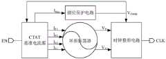
图1是本发明实施例提供的一种对电源电压和温度变化不敏感的环形振荡电路的结构示意图;FIG1 is a schematic diagram of the structure of a ring oscillator circuit that is insensitive to power supply voltage and temperature changes provided by an embodiment of the present invention;
图2是本发明实施例提供的环形振荡电路中CTAT基准电流源的具体电路实现示意图;2 is a schematic diagram of a specific circuit implementation of a CTAT reference current source in a ring oscillation circuit provided by an embodiment of the present invention;
图3是本发明实施例提供的环形振荡电路中环形振荡器的结构示意图;3 is a schematic diagram of the structure of a ring oscillator in a ring oscillation circuit provided in an embodiment of the present invention;
图4是本发明实施例提供的环形振荡器中第一差分延迟单元的具体电路实现示意图;4 is a schematic diagram of a specific circuit implementation of a first differential delay unit in a ring oscillator provided in an embodiment of the present invention;
图5是本发明实施例提供的环形振荡器中第二差分延迟单元的具体电路实现示意图;5 is a schematic diagram of a specific circuit implementation of a second differential delay unit in a ring oscillator provided in an embodiment of the present invention;
图6是本发明实施例提供的环形振荡器输出的振荡电压波形的示意图;6 is a schematic diagram of an oscillation voltage waveform output by a ring oscillator provided in an embodiment of the present invention;
图7是本发明实施例提供的环形振荡电路中钳位保护电路的具体电路实现示意图;7 is a schematic diagram of a specific circuit implementation of a clamping protection circuit in a ring oscillation circuit provided by an embodiment of the present invention;
图8是本发明实施例提供的环形振荡电路中时钟整形电路的具体电路实现示意图。FIG. 8 is a schematic diagram of a specific circuit implementation of a clock shaping circuit in a ring oscillation circuit provided in an embodiment of the present invention.
具体实施方式DETAILED DESCRIPTION
下面结合具体实施例对本发明做进一步详细的描述,但本发明的实施方式不限于此。The present invention is further described in detail below with reference to specific embodiments, but the embodiments of the present invention are not limited thereto.
实施例一Embodiment 1
为了使环形振荡电路输出稳定的时钟信号,请参见图1,本发明实施例提出了一种对电源电压和温度变化不敏感的环形振荡电路,包括CTAT基准电流源、环形振荡器、钳位保护电路和时钟整形电路,其中,In order to make the ring oscillator circuit output a stable clock signal, referring to FIG1 , an embodiment of the present invention proposes a ring oscillator circuit that is insensitive to power supply voltage and temperature changes, including a CTAT reference current source, a ring oscillator, a clamping protection circuit and a clock shaping circuit, wherein:
CTAT基准电流源,用于根据控制信号生成第一偏置电流和具有负温度系数的第二偏置电流;A CTAT reference current source, used for generating a first bias current and a second bias current having a negative temperature coefficient according to a control signal;
环形振荡器,连接CTAT基准电流源,用于根据第二偏置电流补偿环形振荡器由于温度变化引起的正温度系数输出振荡电压;A ring oscillator connected to a CTAT reference current source for compensating for a positive temperature coefficient output oscillation voltage of the ring oscillator due to temperature variation according to a second bias current;
钳位保护电路,连接CTAT基准电流源,用于根据第一偏置电流生成用于保护CTAT基准电流源、时钟整形电路的钳位电压;A clamping protection circuit, connected to the CTAT reference current source, for generating a clamping voltage for protecting the CTAT reference current source and the clock shaping circuit according to the first bias current;
时钟整形电路,连接环形振荡器和钳位保护电路,用于在钳位电压的保护下,对振荡电压进行整形输出时钟信号;A clock shaping circuit is connected to the ring oscillator and the clamp protection circuit, and is used to shape the oscillation voltage and output a clock signal under the protection of the clamp voltage;
CTAT基准电流源,还连接钳位保护电路,还用于在钳位电压的保护下,根据控制信号自适应更新第一偏置电流和第二偏置电流。The CTAT reference current source is also connected to the clamp protection circuit, and is also used to adaptively update the first bias current and the second bias current according to the control signal under the protection of the clamp voltage.
接下来对环形振荡电路的每一部分进行详细的介绍。Next, each part of the ring oscillator circuit is introduced in detail.
请参见图2,本发明实施例环形振荡电路中CTAT基准电流源包括晶体管Mp1~晶体管Mp9、晶体管Mn1~晶体管Mn7、电阻R1和电阻R2,其中,晶体管Mp1的源极、晶体管Mp2的源极、晶体管Mp3的源极、晶体管Mp5的源极、晶体管Mp6的源极与漏极、晶体管Mp8的源极与栅极、电阻R2的一端均连接电源电压VDD,晶体管Mp1的栅极与晶体管Mp2的栅极、晶体管Mp3的栅极、晶体管Mp5的栅极、晶体管Mp2的漏极、晶体管Mn2的漏极连接,晶体管Mp1的漏极与晶体管Mp7的漏极、晶体管Mp9的漏极、晶体管Mn1的漏极、晶体管Mn1~晶体管Mn6的栅极连接,晶体管Mp3的漏极与钳位保护电路的输入端连接,晶体管Mp4的源极与晶体管Mp4的衬底、晶体管Mn1的源极连接,晶体管Mp4的栅极与漏极、晶体管Mn7的源极、电阻R1的一端均连接地电位GND,晶体管Mp5的漏极与晶体管Mp6的栅极、晶体管Mp7的栅极、晶体管Mn7的漏极连接,晶体管Mp7的源极与电阻R2的另一端连接,晶体管Mp8的漏极与晶体管Mp9的源极连接,晶体管Mp9的栅极与钳位保护电路的输出端连接,晶体管Mn2的源极与晶体管Mn3的源极、晶体管Mn4的源极、晶体管Mn5的源极、晶体管Mn6的源极、电阻R1的另一端连接,晶体管Mn3的漏极、晶体管Mn4的漏极、晶体管Mn5的漏极、晶体管Mn6的漏极分别与环形振荡器的第一输入端、第二输入端、第三输入端、第四输入端连接,晶体管Mn7的栅极与控制信号输入端连接。Please refer to FIG2 . The CTAT reference current source in the ring oscillation circuit of the embodiment of the present invention includes transistors Mp1 to Mp9 , transistors Mn1 to Mn7 , resistors R1 and R2 . The source of transistor Mp1 , the source of transistor M p2, the source of transistor Mp3 , the source of transistor Mp5 , the source and drain of transistor Mp6 , the source and gate of transistor Mp8 , and one end of resistor R2 are all connected to the power supply voltage VDD. The gate of transistor Mp1 is connected to the gate of transistor M p2, the gate of transistor M p3, the gate of transistor M p5, the drain of transistor M p2, and the drain of transistor M n2. The drain of transistor M p1isconnectedtothedrainof transistor M p7, the drain of transistor M p9,the drain of transistor Mn1 , and the gates of transistors Mn1 to M n6. The drain of transistor M p3 is connected to the input end of the clamp protection circuit. The source of transistor M p4 is connected to the substrate of transistor M p4, the gate of transistor Mp5 is connected to the substrate of transistor Mp6 , and the drain of transistor Mp7 is connected to the substrate of transistor Mp7 . The source of transistorM n2 is connected to the source of transistor Mn3 , the source of transistor Mn4 , the source of transistor Mn5 , the source of transistor Mn6 , and the other end ofthe resistor R 1, the drain of transistor M n3,thedrainof transistor Mn4, the drain of transistorMn5, and the drain of transistor Mn6 are connected to the first input terminal, the second input terminal, thethird input terminal, and thefourthinput terminal ofthe ringoscillator respectively, and the gate of transistor Mn7 is connected to the control signal input terminal.
具体而言,为了使环形振荡器的整体功耗极低,本发明实施例要求CTAT基准电流源中的晶体管Mn1~晶体管Mn6处于亚阈值区,以及晶体管Mp4也处于亚阈值区,从而可以提供纳安量级的偏置电流。对于处于亚阈值区MOS管的源漏极电流表达式为:Specifically, in order to make the overall power consumption of the ring oscillator extremely low, the embodiment of the present invention requires that the transistorsMn1 toMn6 in the CTAT reference current source are in the subthreshold region, and the transistorMp4 is also in the subthreshold region, so that a bias current of the nanoampere level can be provided. The source-drain current expression of the MOS tube in the subthreshold region is:

其中,I为亚阈值区MOS管的源漏极电流,本发明实施例图2中的电流Iref、电流Iref_mir、电流IP1、电流IP2、电流IN1、电流IN2均为亚阈值区MOS管输出的电流,均可以通过公式(1)计算得到,公式(1)对PMOS型管和NMOS型管均适用;W/L为MOS管的宽长比;I0为单位饱和电流;VT=kT/q称为电压当量,k≈1.38×10-23J/K为玻尔兹曼常数,T为热力学温度,q≈1.6×10-19C为元电荷,常温下VT≈26mV;ξ是亚阈值斜率因子,ξ≈2,其值与工艺参数和管子尺寸有关;VGS为亚阈值区MOS管的栅极电压与源极电压的差值;VDS为亚阈值区MOS管的漏极电压与源极电压的差值。Wherein, I is the source-drain current of the subthreshold region MOS tube. The current Iref , current Iref_mir , current IP1 , current IP2 , current IN1 , and current IN2 in FIG. 2 of the embodiment of the present invention are all currents output by the subthreshold region MOS tube, and can all be calculated by formula (1). Formula (1) is applicable to both PMOS tubes and NMOS tubes. W/L is the width-to-length ratio of the MOS tube. I0 is the unit saturation current. VT = kT/q is called the voltage equivalent, k≈1.38×10⁻²³ J/K is the Boltzmann constant, T is the thermodynamic temperature, q≈1.6×10⁻¹⁹ C is the elementary charge, and VT ≈26 mV at room temperature. ξ is the subthreshold slope factor, ξ≈2, and its value is related to the process parameters and the tube size. VGS is the difference between the gate voltage and the source voltage of the subthreshold region MOS tube. VDS is the difference between the drain voltage and the source voltage of the subthreshold region MOS tube.
由于本发明实施例设计亚阈值区MOS管可以为倒比管,即W/L小于1,则|VDS|远大于VT,因此,亚阈值区MOS管的源漏极电流表达式可化简为:Since the subthreshold MOS transistor in the embodiment of the present invention can be an inverse ratio transistor, that is, W/L is less than 1, |VDS | is much larger than VT , and therefore, the source-drain current expression of the subthreshold MOS transistor can be simplified as:

在CTAT基准电流源中,晶体管Mp1与晶体管Mp2、晶体管Mp3、晶体管Mp5构成一组PMOS电流镜,晶体管Mn1与晶体管Mn2、晶体管Mn3、晶体管Mn4、晶体管Mn5、晶体管Mn6构成一组NMOS电流镜。其中,为了提高电流镜精度并减少噪声,本发明实施例选择晶体管长度和宽度对应相等的晶体管Mp1和晶体管Mp2,晶体管Mp3、晶体管Mp5与晶体管Mp1的长度和宽度对应成比例,晶体管Mn1与晶体管Mn2、晶体管Mn3、晶体管Mn4、晶体管Mn5、晶体管Mn6的长度和宽度对应相等,则电流镜像比例均为1,即Iref=Iref_mir=IP2=IN2=IN1=IP1。其中,尺寸均表示MOS管的宽长比。In the CTAT reference current source, transistorMp1 , transistorMp2 , transistorMp3 , and transistorMp5 form a group of PMOS current mirrors, and transistorMn1 , transistorMn2 , transistorMn3 , transistorMn4 , transistorMn5 , and transistorMn6 form a group of NMOS current mirrors. In order to improve the accuracy of the current mirror and reduce noise, the embodiment of the present invention selects transistorsMp1 and transistorMp2 with equal lengths and widths, transistorsMp3 and transistorMp5 are proportional to the lengths and widths of transistorMp1 , and transistorMn1 and transistorsMn2 , transistorMn3 , transistorMn4 , transistorMn5 , and transistorMn6 have equal lengths and widths, then the current mirror ratios are all 1, that is,Iref =Iref_mir =Ip2 =In2 =In1 =Ip1 . In which, the dimensions all represent the width-to-length ratio of the MOS tube.
由于Iref=Iref_mir,且晶体管Mn1与晶体管Mn2的长度和宽度对应相等,则有


其中,VTC满足下式:Among them, VTC satisfies the following formula:

为了表达VTC的温度特性,则通过VTC对T求偏导数可得:In order to express the temperature characteristics of VTC , the partial derivative of VTC with respect to T can be obtained:

假设芯片的工作温度为-50℃~150℃,即T∈(223K,423K),VTC在几百毫伏的量级,即


由于

由公式(6)可见,电流Iref只与温度和电阻R1有关,而与电源电压无关,且与温度成负相关,与电阻R1成反比。同时,结合公式(3)(4)(5)(6)可知,晶体管Mp4的尺寸会影响VTC的温度系数,进而影响电流Iref的温度系数。为了达到良好的工艺匹配性以及温度补偿效果,本实施例要求CTAT基准电流源中晶体管Mp4的长和宽均与环形振荡器中晶体管的长和宽一致。It can be seen from formula (6) that the current Iref is only related to the temperature and the resistor R1 , but not to the power supply voltage, and is negatively correlated with the temperature and inversely proportional to the resistor R1. At the same time, combined with formulas (3)(4)(5)(6), it can be seen that the size of the transistor Mp4 will affect the temperature coefficient of VTC , and thus affect the temperature coefficient of the current Iref . In order to achieve good process matching and temperature compensation effect, this embodiment requires that the length and width of the transistor Mp4 in the CTAT reference current source are consistent with the length and width of the transistor in the ring oscillator.
本发明实施例设计的CTAT基准电流源可以输出负温度系数的第二偏置电流并且对电源电压不敏感,可以通过增大电阻R1的方式来减小偏置电流,通过增大晶体管Mp4的宽长比(W/L)来增大偏置电流的负温度系数的绝对值,而通过减小电阻R1的方式来增大偏置电流,通过减小晶体管Mp4的宽长比(W/L)来减小偏置电流的负温度系数的绝对值。The CTAT reference current source designed in the embodiment of the present invention can output a second bias current with a negative temperature coefficient and is insensitive to the power supply voltage. The bias current can be reduced by increasing the resistorR1 , and the absolute value of the negative temperature coefficient of the bias current can be increased by increasing the width-to-length ratio (W/L) of the transistor Mp4 . The bias current can be increased by reducing the resistorR1 , and the absolute value of the negative temperature coefficient of the bias current can be reduced by reducing the width-to-length ratio (W/L) of the transistor Mp4 .
进一步地,本发明实施例CTAT基准电流源中PMOS型晶体管Mp5、晶体管Mp6、晶体管Mp7与NMOS型晶体管Mn7、电阻R2构成了启动电路,可以破坏CTAT基准电流源中的简并点。其中,晶体管Mn7为开关管,晶体管Mp6为MOS电容。当控制信号输入端EN输入一个脉冲信号时,启动电路开始工作:当该脉冲信号从低电平变成高电平时,晶体管Mn7导通,对晶体管Mp6放电,直至启动电压Vst降为地电位GND。此时,晶体管Mp7导通并输出启动电流Ist,成为电流Iref的一部分,打破CTAT基准电流源的简并点,并产生偏置电流,这里偏置电流包括在晶体管Mp3处产生的第一偏置电流Ibias,第一偏置电流Ibias用于产生钳位电压,以及在晶体管Mn3、晶体管Mn4、晶体管Mn5、晶体管Mn6处分别产生的第二偏置电流,其中,第二偏置电流包括在晶体管Mn6处产生的电流IP1、在晶体管Mn3处产生的电流IP2、在晶体管Mn5处产生的电流IN1、在晶体管Mn4处产生的电流IN2,电流IP1、电流IP2、电流IN1、电流IN2用于为环形振荡器提供工作电流;当该脉冲信号从高电平变成低电平时,晶体管Mn7关断,晶体管Mp5产生的偏置电流开始对晶体管Mp6充电,直至启动电压Vst升高至电源电压VDD,此时,启动电路工作完成,CTAT基准电流源电路趋于稳定。Furthermore, in the CTAT reference current source of the embodiment of the present invention, the PMOS transistorMp5 , the transistorMp6 , the transistorMp7 , the NMOS transistorMn7 , and the resistorR2 form a startup circuit, which can destroy the degeneracy point in the CTAT reference current source. Among them, the transistorMn7 is a switch tube, and the transistorMp6 is a MOS capacitor. When a pulse signal is input to the control signal input terminal EN, the startup circuit starts to work: when the pulse signal changes from a low level to a high level, the transistorMn7 is turned on, and the transistorMp6 is discharged until the startup voltageVst drops to the ground potential GND. At this time, transistor Mp7 is turned on and outputs a startup current Ist , which becomes a part of the current Iref , breaks the degeneracy point of the CTAT reference current source, and generates a bias current, where the bias current includes a first bias current Ibias generated at transistor Mp3 , the first bias current Ibias is used to generate a clamping voltage, and second bias currents generated at transistors Mn3 , Mn4 , Mn5 , and Mn6 , respectively, where the second bias current includes a current IP1 generated at transistor Mn6 , a current IP2 generated at transistor Mn3 , a current IN1 generated at transistor Mn5 , and a current IN2 generated at transistor Mn4 , and currents IP1 , IP2 , IN1 , and I N2are used to provide a working current for the ring oscillator; when the pulse signal changes from a high level to a low level, transistor Mn7 is turned off, and the bias current generated by transistor Mp5 starts to charge transistor Mp6 until the startup voltage Vst rises to the power supply voltage VDD, at which point the startup circuit is completed and the CTAT reference current source circuit becomes stable.
随着温度的不断升高,MOS管的泄漏电流会急剧升高。因此,为了补偿高温下环形振荡器中晶体管(PMOS)的泄露电流,本发明实施例设计了由PMOS型晶体管Mp8、晶体管Mp9组成的泄露电流补偿电路。由于晶体管Mp8的栅极与源极相连,始终处于关断状态,从而输出泄露补偿电流Icom。为了达到良好的工艺匹配与泄漏电流补偿作用,本发明实施例要求CTAT基准电流源中晶体管Mp8的长和宽均与环形振荡器中晶体管的长和宽一致;晶体管Mp9的栅极输入钳位电压Vclamp,用于防止晶体管Mp8被击穿,从而使得CTAT基准电流源可以工作在较大的电压下,对电源电压不敏感。As the temperature continues to rise, the leakage current of the MOS tube will increase sharply. Therefore, in order to compensate for the leakage current of the transistor (PMOS) in the ring oscillator at high temperature, the embodiment of the present invention designs a leakage current compensation circuit composed of a PMOS transistor Mp8 and a transistor Mp9 . Since the gate of the transistor Mp8 is connected to the source, it is always in an off state, thereby outputting a leakage compensation current Icom . In order to achieve good process matching and leakage current compensation, the embodiment of the present invention requires that the length and width of the transistor Mp8 in the CTAT reference current source are consistent with the length and width of the transistor in the ring oscillator; the gate of the transistor Mp9 inputs a clamping voltage Vclamp , which is used to prevent the transistor Mp8 from being broken down, so that the CTAT reference current source can operate at a larger voltage and is insensitive to the power supply voltage.
除了CTAT基准电流源中晶体管Mn1~晶体管Mn6、晶体管Mp4处于亚阈值区设计外,为了进一步减小功耗,本发明实施例还采用了电流复用技术,具体地:分别流过晶体管Mn3、晶体管Mn4、晶体管Mn5、晶体管Mn6的偏置电流IP2、电流IN2、电流IN1、IP1电流与流过晶体管Mn2的电流Iref_mir一起流过电阻R1,以产生电压VTC_MIR,从而有效减小了Iref_mir的大小,降低了电路功耗。In addition to the sub-threshold region design of transistorsMn1 toMn6 and transistorMp4 in the CTAT reference current source, in order to further reduce power consumption, the embodiment of the present invention also adopts a current multiplexing technology. Specifically, the bias current IP2 , the current IN2 , the current IN1 , and the IP1 current flowing through the transistorMn3 , the transistorMn4 , the transistorMn5 , and the transistorMn6 respectively flow through the resistorR1 together with the current Iref_mir flowing through the transistorMn2 to generate a voltage VTC_MIR , thereby effectively reducing the size of Iref_mir and reducing the power consumption of the circuit.
可见,本发明实施例中CTAT基准电流源可以产生负温度系数的偏置电流,且对电源电压不敏感;同时,CTAT基准电流源还可以补偿高温下的泄漏电流并具有较低的功耗。It can be seen that the CTAT reference current source in the embodiment of the present invention can generate a bias current with a negative temperature coefficient and is insensitive to the power supply voltage; at the same time, the CTAT reference current source can also compensate for the leakage current at high temperature and has lower power consumption.
进一步地,请参见图3,本发明实施例环形振荡器包括第一差分延迟单元DLY1和第二差分延迟单元DLY2,其中,第一差分延迟单元DLY1的正相输入端与第二差分延迟单元DLY2的反相输出端、环形振荡器的第四输入端、时钟整形电路的第一输入端连接,第一差分延迟单元DLY1的反相输入端与第二差分延迟单元DLY2的正相输出端、环形振荡器的第三输入端、时钟整形电路的第二输入端连接,第一差分延迟单元DLY1的正相输出端与环形振荡器的第一输入端、第二差分延迟单元DLY2的正相输入端连接,第一差分延迟单元DLY1的反相输出端与环形振荡器的第二输入端、第二差分延迟单元DLY2的反相输入端连接。本发明实施例环形振荡器采用两级差分延迟单元结构,每级提供90°的相位偏移。为了确保环形振荡器能够稳定振荡,第一差分延迟单元DLY1的输出端与第二差分延迟单元的输入端DLY2同相连接,第二差分延迟单元DLY2的输出端与第一差分延迟单元DLY1的输入端反向连接,使得两级差分延迟单元共产生180°的相位偏移,即振荡电压VP1与振荡电压VP2存在相位偏移,振荡电压VN1与振荡电压VN2存在180°相位偏移。Further, referring to FIG. 3 , the ring oscillator of the embodiment of the present invention comprises a first differential delay unit DLY1 and a second differential delay unit DLY2, wherein the positive phase input terminal of the first differential delay unit DLY1 is connected to the negative phase output terminal of the second differential delay unit DLY2, the fourth input terminal of the ring oscillator, and the first input terminal of the clock shaping circuit, the negative phase input terminal of the first differential delay unit DLY1 is connected to the positive phase output terminal of the second differential delay unit DLY2, the third input terminal of the ring oscillator, and the second input terminal of the clock shaping circuit, the positive phase output terminal of the first differential delay unit DLY1 is connected to the first input terminal of the ring oscillator and the positive phase input terminal of the second differential delay unit DLY2, and the negative phase output terminal of the first differential delay unit DLY1 is connected to the second input terminal of the ring oscillator and the negative phase input terminal of the second differential delay unit DLY2. The ring oscillator of the embodiment of the present invention adopts a two-stage differential delay unit structure, and each stage provides a 90° phase shift. In order to ensure that the ring oscillator can oscillate stably, the output end of the first differential delay unit DLY1 is connected in phase with the input end DLY2 of the second differential delay unit, and the output end of the second differential delay unit DLY2 is connected in reverse to the input end of the first differential delay unit DLY1, so that the two-stage differential delay units produce a total phase shift of 180°, that is, there is a phase shift between the oscillation voltageVP1 and the oscillation voltageVP2 , and there is a 180° phase shift between the oscillation voltageVN1 and the oscillation voltageVN2 .
接下来,分别对环形振荡器中第一差分延迟单元DLY1和第二差分延迟单元DLY2进行详细介绍。Next, the first differential delay unit DLY1 and the second differential delay unit DLY2 in the ring oscillator are respectively introduced in detail.
请参见图4,本发明实施例第一差分延迟单元DLY1包括晶体管Mp10~晶体管Mp17,其中,晶体管Mp10的源极、晶体管Mp11的源极、晶体管Mp13的源极、晶体管Mp14的源极、晶体管Mp15的源极、晶体管Mp17的源极均连接电源电压VDD;晶体管Mp10的栅极与晶体管Mp14的漏极、晶体管Mp16的漏极、晶体管Mp17的漏极、晶体管Mp15的栅极、晶体管Mp16的栅极、第二差分延迟单元DLY2的正相输入端连接,晶体管Mp10的漏极与晶体管Mp12的漏极、晶体管Mp13的漏极、晶体管Mp11的栅极、晶体管Mp12的栅极、晶体管Mp14的栅极、第二差分延迟单元DLY2的反相输入端连接,晶体管Mp11的漏极与晶体管Mp12的源极连接,晶体管Mp13的栅极与第二差分延迟单元DLY2的反相输出端连接,晶体管Mp17的栅极与第二差分延迟单元DLY2的正相输出端连接,晶体管Mp15的漏极与晶体管Mp16的源极连接。Please refer to FIG4 . The first differential delay unit DLY1 of the embodiment of the present invention includes transistors Mp10 to Mp17 , wherein the source of transistor Mp10 , the source of transistor Mp11 , the source of transistor Mp13 , the source of transistor M p14, the source of transistor Mp15 , and the source of transistor Mp17 are all connected to the power supply voltage VDD; the gate of transistor Mp10 is connected to the drain oftransistor Mp14 , the drain of transistor M p16, the drain of transistor Mp17 , the gate of transistor Mp15 , the gate of transistor Mp16 , and the non-inverting input terminal of the second differential delay unit DLY2; the drain of transistor Mp10 is connected to the drain of transistor Mp12 , the drain of transistor Mp13 , the gate of transistor Mp11 , the gate of transistor Mp12 , the gate of transistor Mp14 , and the inverting input terminal of the second differential delay unit DLY2; the drain of transistor Mp11 is connected to the source of transistor M p12, and the gate of transistor Mp17 is connected to the gate of transistor Mp15. The gate of transistorM p13 is connected to the inverting output terminal of the second differential delay unit DLY2 , the gate of transistor Mp17 is connected to the non-inverting output terminal of the second differential delay unit DLY2 , and the drain of transistor Mp15 is connected to the source of transistor Mp16 .
具体而言,PMOS型晶体管Mp13、晶体管Mp17为第一差分延迟单元DLY1的输入对管,其宽长比对环形振荡器的输出频率具有决定性作用,宽长比越大,寄生电容的充电电流越大,则输出振荡频率越快;PMOS型晶体管Mp11、晶体管Mp12与晶体管Mp15、晶体管Mp16为有源负载对,其主要通过调节寄生电容的放电电流的大小来调节输出振荡频率,具体地:有源负载对的宽长比越大,有源电阻越小,流过有源负载的电流越大,寄生电容的放电电流越小,则输出振荡频率就越低;有源负载对的宽长比越小,有源电阻越大,流过有源负载的电流越小,寄生电容的放电电流越大,则输出振荡频率就越高;PMOS型晶体管Mp10、晶体管Mp14为交叉耦合管,面积越大,则其栅电容等寄生电容越大,进而输出振荡频率越低,晶体管Mp10、晶体管Mp14为第一差分延迟单元DLY1引入正反馈,使得两级差分延迟单元能够正常起振并减小输出波形的跃变时间。Specifically, the PMOS transistorMp13 and the transistorMp17 are input pairs of the first differential delay unit DLY1, and their width-to-length ratio plays a decisive role in the output frequency of the ring oscillator. The larger the width-to-length ratio, the larger the charging current of the parasitic capacitance, and the faster the output oscillation frequency; the PMOS transistorMp11 , the transistorMp12 and the transistorMp15 , the transistorMp16 are active load pairs, which mainly adjust the output oscillation frequency by adjusting the discharge current of the parasitic capacitance. Specifically: the larger the width-to-length ratio of the active load pair, the smaller the active resistance, the larger the current flowing through the active load, the smaller the discharge current of the parasitic capacitance, and the lower the output oscillation frequency; the smaller the width-to-length ratio of the active load pair, the larger the active resistance, the smaller the current flowing through the active load, the larger the discharge current of the parasitic capacitance, and the higher the output oscillation frequency; the PMOS transistorMp10 and the transistorMp14 are cross-coupled transistors, and the larger the area, the larger the parasitic capacitance such as the gate capacitance, and thus the lower the output oscillation frequency, and the transistor Mp15 is connected to the transistor Mp16.p10 and transistor Mp14 introduce positive feedback into the first differential delay unit DLY1 , so that the two-stage differential delay unit can start oscillating normally and reduce the transition time of the output waveform.
请参见图5,本发明实施例第二差分延迟单元DLY2包括晶体管Mp18~晶体管Mp27,其中,晶体管Mp18的源极、晶体管Mp19的源极、晶体管Mp21的源极、晶体管Mp22的源极、晶体管Mp23的源极、晶体管Mp24的源极、晶体管Mp26的源极、晶体管Mp27的源极、晶体管Mp21的漏极、晶体管Mp26的漏极均连接电源电压VDD,晶体管Mp18的栅极与晶体管Mp24的栅极、晶体管Mp25的栅极、晶体管Mp23的漏极、晶体管Mp25的漏极、晶体管Mp27的漏极、第一差分延迟单元DLY1的反相输入端连接,晶体管Mp18的漏极与晶体管Mp19的栅极、晶体管Mp20的栅极、晶体管Mp23的栅极、晶体管Mp20的漏极、晶体管Mp22的漏极、第一差分延迟单元DLY1的正相输入端连接,晶体管Mp19的漏极与晶体管Mp20的源极连接,晶体管Mp21的栅极与晶体管Mp22的栅极、第一差分延迟单元DLY1的正相输出端连接,晶体管Mp24的漏极与晶体管Mp25的源极连接,晶体管Mp26的栅极与晶体管Mp27的栅极、第一差分延迟单元DLY1的反相输出端连接。Please refer to FIG5 . The second differential delay unit DLY2 of the embodiment of the present invention includes transistors Mp18 to Mp27 , wherein the source of transistor Mp18 , the source of transistor Mp19 , the source of transistor Mp21 , the source of transistor Mp22 , the source of transistor Mp23 , the source of transistor Mp24 , the source of transistor Mp26, the source of transistor M p27 , the drain of transistor Mp21 , and the drain of transistor Mp26 are all connected to the power supply voltage VDD, the gate of transistor Mp18 is connected to the gate of transistor Mp24 , the gate of transistor Mp25 , the drain of transistor Mp23 , the drain of transistor Mp25 , and the inverting input terminal of the first differential delay unit DLY1, and the drain of transistor Mp18 is connectedto the gate of transistor Mp19 , the gate of transistor Mp20 , the gate of transistor Mp23 , the drain of transistor Mp20 , and the drain of transistor Mp24 . The drain of transistorM p22 is connected to the non-inverting input terminal of the first differential delay unit DLY1, the drain of transistor Mp19 is connected to the source of transistor Mp20 , the gate of transistor Mp21 is connected to the gate of transistor Mp22 and the non-inverting output terminal of the first differential delay unit DLY1, the drain of transistor Mp24 is connected to the source of transistor Mp25 , and the gate of transistor Mp26 is connected to the gate of transistor Mp27 and the inverting output terminal of the first differential delay unit DLY1.
具体而言,本发明实施例第二差分延迟单元DLY2的结构以及工作原理与第一差分延迟单元DLY1几乎相同,Mp18~晶体管Mp20、晶体管Mp22~晶体管Mp25、晶体管Mp27也为PMOS型晶体管,唯一的区别是多了两个PMOS型晶体管Mp21、晶体管Mp26,晶体管Mp21、晶体管Mp26均为MOS电容,其晶体管的长和宽与时钟整形电路中输入对管的长和宽一致,用于等效输入对管的栅电容等寄生电容,使得两级差分延迟单元的负载电容尽可能一致。Specifically, the structure and working principle of the second differential delay unit DLY2 in the embodiment of the present invention are almost the same as those of the first differential delay unit DLY1. TransistorMp18 to transistorMp20 , transistorMp22 to transistorMp25 , and transistorMp27 are also PMOS transistors. The only difference is that there are two more PMOS transistorsMp21 and transistorMp26 . TransistorMp21 and transistorMp26 are both MOS capacitors. The length and width of the transistors are consistent with the length and width of the input pair tube in the clock shaping circuit, and are used to equivalent parasitic capacitances such as the gate capacitance of the input pair tube, so that the load capacitances of the two-stage differential delay units are as consistent as possible.
为了保证良好的工艺匹配性,优选环形振荡器中所有PMOS型管的尺寸均一致,即第一差分延迟单元DLY1和第二差分延迟单元DLY2中所有PMOS型管的长和宽一致。In order to ensure good process matching, it is preferred that the sizes of all PMOS tubes in the ring oscillator are consistent, that is, the lengths and widths of all PMOS tubes in the first differential delay unit DLY1 and the second differential delay unit DLY2 are consistent.
本发明实施例环形振荡器的输出振荡频率对电源电压VDD不敏感,具体分析如下:The output oscillation frequency of the ring oscillator in the embodiment of the present invention is insensitive to the power supply voltage VDD, and the specific analysis is as follows:
请参见图6,以环形振荡器的振荡电压波形进行说明,本发明实施例由于PMOS型管仅工作在亚阈值区或者截止区,使得环形振荡器的偏置电流极低,振荡摆幅由PMOS型管的阈值电压Vthp决定,摆幅范围约为VDD-|Vthp|~VDD。记下降时间为TDN,上升时间为TUP。由于交叉耦合管的正反馈作用,振荡电压在半个振荡周期内始终保持在电源电压VDD,该段时间记为保持时间THD。如图6所示,假设环形振荡器电路在t1时刻以后进入稳定振荡状态,且振荡电压从电源电压VDD开始下降。Please refer to FIG6 , which uses the oscillation voltage waveform of the ring oscillator for illustration. In the embodiment of the present invention, since the PMOS tube only works in the subthreshold region or the cut-off region, the bias current of the ring oscillator is extremely low, and the oscillation amplitude is determined by the threshold voltage Vthp of the PMOS tube, and the amplitude range is approximately VDD-|Vthp |~VDD. The falling time is recorded as TDN , and the rising time is recorded as TUP . Due to the positive feedback effect of the cross-coupled tube, the oscillation voltage is always maintained at the power supply voltage VDD within half an oscillation cycle, and this period of time is recorded as the holding time THD . As shown in FIG6 , it is assumed that the ring oscillator circuit enters a stable oscillation state after time t1 , and the oscillation voltage starts to drop from the power supply voltage VDD.
环形振荡器振荡电压的下降时间主要与振荡摆幅、有源电阻、偏置电流以及负载电容有关,且对环形振荡器的输出频率起决定性作用。振荡摆幅越大,则意味着寄生电容所需放电的电压越高,从而下降时间越长;振荡摆幅越小,则意味着寄生电容所需放电的电压越低,从而下降时间越短。有源电阻和偏置电流主要通过影响寄生电容的放电电流大小来影响下降时间。有源电阻越大,流过有源电阻的电流越小,偏置电流越大,则寄生电容放电的电流越大,下降时间越短;有源电阻越小,流过有源电阻的电流越大,偏置电流越小,则寄生电容放电的电流越小,下降时间越长。此外,随着振荡电压的不断降低,有源电阻两边的电压会不断变大,流过有源电阻的电流也会不断变大,使得寄生电容的放电电流不断减小,因此放电时振荡电压斜率的绝对值是不断减小的。负载电容主要通过影响寄生电容的放电电荷多少来影响下降时间。假设振荡摆幅与寄生电容的放电电流恒定,负载电容越大,则寄生电容所需放电的电荷越多,下降时间就越长,同理,负载电容越小,则寄生电容所需放电的电荷越少,下降时间就越短。The fall time of the oscillation voltage of the ring oscillator is mainly related to the oscillation swing, active resistance, bias current and load capacitance, and plays a decisive role in the output frequency of the ring oscillator. The larger the oscillation swing, the higher the voltage required to discharge the parasitic capacitance, and the longer the fall time; the smaller the oscillation swing, the lower the voltage required to discharge the parasitic capacitance, and the shorter the fall time. The active resistance and bias current mainly affect the fall time by affecting the discharge current of the parasitic capacitance. The larger the active resistance, the smaller the current flowing through the active resistance, the larger the bias current, the larger the current discharged by the parasitic capacitance, and the shorter the fall time; the smaller the active resistance, the larger the current flowing through the active resistance, the smaller the bias current, the smaller the current discharged by the parasitic capacitance, and the longer the fall time. In addition, as the oscillation voltage continues to decrease, the voltage on both sides of the active resistance will continue to increase, and the current flowing through the active resistance will continue to increase, causing the discharge current of the parasitic capacitance to continue to decrease, so the absolute value of the oscillation voltage slope during discharge is constantly decreasing. The load capacitance mainly affects the fall time by affecting the discharge charge of the parasitic capacitance. Assuming that the oscillation swing and the discharge current of the parasitic capacitance are constant, the larger the load capacitance, the more charge the parasitic capacitance needs to discharge and the longer the fall time. Similarly, the smaller the load capacitance, the less charge the parasitic capacitance needs to discharge and the shorter the fall time.
环形振荡器振荡电压的上升时间主要与输入对管、振荡摆幅、有源电阻、偏置电流以及负载电容有关。其中,由于流过输入对管的电流一般会远大于偏置电流,因此输入对管的宽长比对上升时间起决定性作用,且上升时间占振荡周期的比例很小。输入对管通过影响寄生电容充电电流的大小来影响上升时间。输入对管的宽长比越大,则寄生电容充电电流越大,上升时间就越短;输入对管的宽长比越小,则寄生电容充电电流越小,上升时间就越长。振荡摆幅、有源电阻、偏置电流以及负载电容对上升时间的影响机理与对下降时间的影响机理类似。振荡摆幅越大,有源电阻越大,偏置电流越大,负载电容越大,则上升时间就越长;振荡摆幅越小,有源电阻越小,偏置电流越小,负载电容越小,则上升时间就越短。The rise time of the oscillation voltage of the ring oscillator is mainly related to the input pair tube, oscillation swing, active resistance, bias current and load capacitance. Among them, since the current flowing through the input pair tube is generally much larger than the bias current, the width-to-length ratio of the input pair tube plays a decisive role in the rise time, and the rise time accounts for a very small proportion of the oscillation period. The input pair tube affects the rise time by affecting the magnitude of the parasitic capacitance charging current. The larger the width-to-length ratio of the input pair tube, the larger the parasitic capacitance charging current and the shorter the rise time; the smaller the width-to-length ratio of the input pair tube, the smaller the parasitic capacitance charging current and the longer the rise time. The influence mechanism of the oscillation swing, active resistance, bias current and load capacitance on the rise time is similar to the influence mechanism on the fall time. The larger the oscillation swing, the larger the active resistance, the larger the bias current and the larger the load capacitance, the longer the rise time; the smaller the oscillation swing, the smaller the active resistance, the smaller the bias current and the smaller the load capacitance, the shorter the rise time.
上升时间与下降时间可以简单表述为:The rise time and fall time can be simply expressed as:

其中,Cpa为寄生电容,Usw为振荡摆幅,

由公式(8)可以看出,环形振荡器的振荡频率主要由下降时间TDN决定。此外,公式(8)中所有变量均与电源电压VDD无关,说明该环形振荡器的输出振荡频率对电源电压VDD不敏感。It can be seen from formula (8) that the oscillation frequency of the ring oscillator is mainly determined by the fall time TDN . In addition, all variables in formula (8) are independent of the power supply voltage VDD, indicating that the output oscillation frequency of the ring oscillator is insensitive to the power supply voltage VDD.
本发明实施例环形振荡器的输出振荡频率具有正温度系数,具体分析如下:The output oscillation frequency of the ring oscillator in the embodiment of the present invention has a positive temperature coefficient, which is specifically analyzed as follows:
对于任意PMOS型管的阈值电压主要由半导体内的少子浓度、栅氧化层电荷及其厚度等因素决定。对于任意PMOS型管的阈值电压Vthp可表达为:The threshold voltage of any PMOS transistor is mainly determined by the minority carrier concentration in the semiconductor, the charge and thickness of the gate oxide layer, etc. The threshold voltage Vthp of any PMOS transistor can be expressed as:

其中,Vms为栅与衬底间的接触电势差;Vfn为n型衬底的静电势;Qbo为单位面积的栅电荷量;Qss为表面态界面的参考电荷量,是一个常量;Cox为单位面积的栅氧化层电容;εsi为硅的介电常数;ni为硅的本征载流子浓度;ND为n型衬底的掺杂浓度;VG为栅电势;Npoly为栅掺杂浓度;k为玻尔兹曼常数;T为热力学温度;q为元电荷量。Among them,Vms is the contact potential difference between the gate and the substrate;Vfn is the electrostatic potential of the n-type substrate;Qbo is the gate charge per unit area;Qss is the reference charge of the surface state interface, which is a constant;Cox is the gate oxide capacitance per unit area;εsi is the dielectric constant of silicon; ni is the intrinsic carrier concentration of silicon;ND is the doping concentration of the n-type substrate;VG is the gate potential;Npoly is the gate doping concentration; k is the Boltzmann constant; T is the thermodynamic temperature; q is the elementary charge.
为了表达Vthp的温度特性,则通过Vthp对T求偏导数可得:In order to express the temperature characteristics of Vthp , the partial derivative of Vthp with respect to T can be obtained:

通常,栅掺杂浓度Npoly远大于n型衬底的掺杂浓度ND,故

对于任意有源电阻可表达为:For any active resistor, it can be expressed as:

为了表达Ron的温度特性,则通过Ron对T求偏导数可得:In order to express the temperature characteristics of Ron , the partial derivative of Ron with respect to T can be obtained:

在公式(12)中,ξ≈2,

根据上述分析,假设偏置电流不变,当温度升高时,振荡摆幅减小,振荡频率增加,有源电阻减小,振荡频率减小,负载电容几乎不影响振荡频率,而当温度降低时,振荡摆幅增大,振荡频率减小,有源电阻增大,振荡频率增加,负载电容几乎不影响振荡频率。这是一对矛盾的变化。事实上,即使有源电阻会随着温度增加而减小,但其有源电阻仍然过大,流过有源电阻的电流很小,使得有源电阻的影响不如振荡摆幅显著,即当温度升高时,环形振荡器的输出频率会升高,当温度降低时,环形振荡器的输出频率会降低,具有正温度系数。According to the above analysis, assuming that the bias current remains unchanged, when the temperature rises, the oscillation amplitude decreases, the oscillation frequency increases, the active resistance decreases, the oscillation frequency decreases, and the load capacitance has almost no effect on the oscillation frequency. When the temperature decreases, the oscillation amplitude increases, the oscillation frequency decreases, the active resistance increases, the oscillation frequency increases, and the load capacitance has almost no effect on the oscillation frequency. This is a pair of contradictory changes. In fact, even if the active resistance decreases with increasing temperature, its active resistance is still too large, and the current flowing through the active resistance is very small, making the influence of the active resistance less significant than the oscillation amplitude, that is, when the temperature rises, the output frequency of the ring oscillator will increase, and when the temperature decreases, the output frequency of the ring oscillator will decrease, with a positive temperature coefficient.
由公式(12)可知,为了补偿环形振荡器输出频率的正温度系数,可以通过加一负温度系数的放电电流来实现,使得振荡频率对温度变化不敏感。而本发明实施例设计的CTAT基准电流源提供的第二偏置电流恰好具有负温度系数,通过调节晶体管Mp4的尺寸即可对环形振荡器的振荡频率实现良好的温度补偿效果。It can be seen from formula (12) that in order to compensate for the positive temperature coefficient of the output frequency of the ring oscillator, a discharge current with a negative temperature coefficient can be added to make the oscillation frequency insensitive to temperature changes. The second bias current provided by the CTAT reference current source designed in the embodiment of the present invention happens to have a negative temperature coefficient, and a good temperature compensation effect can be achieved for the oscillation frequency of the ring oscillator by adjusting the size of the transistor Mp4 .
进一步地,请参见图7,本发明实施例钳位保护电路包括晶体管Mn8、晶体管Mn9、晶体管Mp28、晶体管Mp29,其中,晶体管Mp29的源极连接电源电压VDD,晶体管Mp29的栅极与晶体管Mp29的漏极、晶体管Mp28的源极连接,晶体管Mp28的栅极与晶体管Mp28的漏极、晶体管Mn9的漏极、钳位保护电路的输出端连接,晶体管Mn9的栅极与晶体管Mn8的栅极、晶体管Mn8的漏极、钳位保护电路的输入端连接,晶体管Mn9的源极、晶体管Mn8的源极均连接地电位GND。Further, referring to FIG. 7 , the clamping protection circuit of the embodiment of the present invention includes a transistor Mn8 , a transistor Mn9 , a transistor Mp28 , and a transistor Mp29 , wherein the source of the transistor Mp29 is connected to the power supply voltage VDD, the gate of the transistor Mp29 is connected to the drain of the transistor Mp29 and the source of the transistor Mp28 , the gate of the transistor Mp28 is connected to the drain of the transistor Mp28 , the drain of the transistor Mn9 , and the output end of the clamping protection circuit, the gate of the transistor Mn9 is connected to the gate of the transistor Mn8 , the drain of the transistor Mn8 , and the input end of the clamping protection circuit, and the source of the transistor Mn9 and the source of the transistor Mn8 are both connected to the ground potential GND.
具体而言,本发明实施例通过NMOS型晶体管Mn8、晶体管Mn9,以及PMOS型晶体管Mp28、晶体管Mp29构成了钳位保护电路,根据CTAT基准电流源输出的第一偏置电流Ibias产生一个跟随电源电压变化的钳位电压Vclamp,用于防止CTAT基准电流源、时钟整形电路中核心管子的源漏两端电压因为过大而击穿,使得CTAT基准电流源、时钟整形电路可以工作在更大的电压下,不受电源电压VDD的影响。其中,晶体管Mp29的长和宽均与晶体管Mp8、晶体管Mp4,以及与环形振荡器中所有的PMOS型管的长和宽一致;晶体管Mp28的长和宽均与晶体管Mp9的长和宽一致。Specifically, the embodiment of the present invention forms a clamp protection circuit through NMOS transistorMn8 , transistorMn9 , and PMOS transistorMp28 , transistorMp29 , and generates a clamp voltage Vclampthat follows the power supply voltage according to the first bias current Ibias output by the CTAT reference current source, which is used to prevent the voltage at both ends of the source and drain of the core tube in the CTAT reference current source and the clock shaping circuit from being broken down due to excessive voltage, so that the CTAT reference current source and the clock shaping circuit can work at a higher voltage and are not affected by the power supply voltage VDD. Among them, the length and width of transistorMp29 are consistent with the length and width of transistorMp8 , transistorMp4 , and all PMOS tubes in the ring oscillator; the length and width of transistorMp28 are consistent with the length and width of transistorMp9 .
进一步地,请参见图8,本发明实施例时钟整形电路包括晶体管Mp30~晶体管Mp38、晶体管Mn10~晶体管Mn18、触发器SMT1、反相器INV1~反相器INV4和缓冲器BUF1,其中,晶体管Mp32的源极、晶体管Mp34的源极、晶体管Mp36的源极、晶体管Mp37的源极、晶体管Mp38的源极均连接电源电压VDD,晶体管Mp37的栅极与第二差分延迟单元DLY2的反相输出端连接,晶体管Mp37的漏极与晶体管Mp30的源极连接,晶体管Mp38的栅极与第二差分延迟单元DLY2的正相输出端连接,晶体管Mp38的漏极与晶体管Mp31的源极连接,晶体管Mp30的栅极与晶体管Mp31的栅极、钳位保护电路的输出端连接,晶体管Mp30的漏极与晶体管Mp33的漏极、晶体管Mn17的漏极、晶体管Mn12的漏极、晶体管Mn18的栅极连接,晶体管Mp31的漏极与晶体管Mp35的漏极、晶体管Mn18的漏极、晶体管Mn14的漏极、晶体管Mn17的栅极、触发器SMT1的输入端连接,晶体管Mp32的栅极与晶体管Mp34的栅极、晶体管Mp36的栅极、晶体管Mp36的漏极、晶体管Mn16的漏极连接,晶体管Mp32的漏极与晶体管Mp33的源极连接,晶体管Mp33的栅极与晶体管Mn12的栅极、反相器INV3的输出端连接,晶体管Mp34的漏极与晶体管Mp35的源极连接,晶体管Mp35的栅极与晶体管Mn14的栅极、反相器INV4的输出端连接,晶体管Mn17的源极与晶体管Mn10的漏极连接,晶体管Mn18的源极与晶体管Mn11的漏极连接,晶体管Mn12的源极与晶体管Mn13的漏极连接,晶体管Mn14的源极与晶体管Mn15的漏极连接,晶体管Mn10的源极与晶体管Mn11的源极、晶体管Mn13的源极、晶体管Mn15的源极、晶体管Mn16的源极均连接地电位GND,晶体管Mn10的栅极与晶体管Mn11的栅极、晶体管Mn13的栅极、晶体管Mn15的栅极、晶体管Mn16的栅极均连接偏置电压Vbn,触发器SMT1的输出端与反相器INV1的输入端连接,反相器INV1的输出端与反相器INV2、反相器INV3的输入端连接,反相器INV2的输出端与反相器INV4、缓冲器BUF1的输入端连接,缓冲器BUF1的输出端为环形振荡电路的最终输出端。其中,本发明实施例偏置电压Vbn可以为钳位保护电路中晶体管Mn8的栅极处的电压,此时晶体管Mn16的栅极与晶体管Mn8的栅极、晶体管Mn9的栅极、钳位保护电路的输入端的连接。Further, referring to FIG8 , the clock shaping circuit of the embodiment of the present invention includes transistors Mp30 to Mp38 , transistors Mn10 to Mn18 , a trigger SMT1, inverters INV1 to INV4, and a buffer BUF1, wherein the source of transistor Mp32 , the source of transistor Mp34 , the source of transistor Mp36 , the source of transistor Mp37 , and the source of transistor M p38 are all connected to the power supply voltage VDD, the gate of transistor Mp37 is connected to the inverting output terminal of the second differential delay unit DLY2, the drain of transistor Mp37 is connected to the source of transistor Mp30 , the gate of transistor Mp38 is connected to the non-inverting output terminal of the second differential delay unit DLY2, the drain of transistor Mp38 is connected to the source of transistor Mp31 , the gate of transistor Mp30 is connected to the gate of transistor M p31 and the output terminal of the clamping protection circuit, and the drain of transistor Mp30 is connected to the gate of transistor Mp31 and the output terminal of the clamping protection circuit. The drain of transistor Mp33 is connected to the drain of transistor Mn17 , the drain of transistor Mn12 , and the gate of transistor Mn18 . The drain of transistor Mp31 is connected to the drain of transistor Mp35 , the drain of transistor Mn18 , the drain of transistor Mn14 , the gate of transistor Mn17 , and the input terminal of trigger SMT1. The gate of transistor Mp32 is connected to the gate of transistor Mp34 , the gate of transistor Mp36 , the drain of transistor Mp36 , and the drain of transistor M n16. The drain of transistor Mp32 is connected to the source of transistor Mp33 . The gate of transistor Mp33 is connected to the gate of transistor Mn12 and the output terminal of inverter INV3. The drain of transistor Mp34 is connected to the source of transistor Mp35. The gate of transistor M p35is connected to the gate of transistor Mn14 and the output terminal of inverter INV4. The source of transistor Mn17 is connected to the drain of transistor Mn10 . The source oftransistor n18 is connected to the drain of transistorMn11 , the source of transistorMn12 is connected to the drain of transistorMn13 , the source of transistorMn14 is connected to the drain of transistorMn15 , the source of transistorMn10 , the source of transistorMn11 , the source of transistorMn13 , the source of transistorMn15 and the source of transistorMn16 are all connected to the ground potential GND, the gate of transistorMn10 , the gate of transistorMn11 , the gate of transistorMn13 , the gate of transistorMn15 and the gate of transistorMn16 are all connected to the bias voltageVbn , the output end of trigger SMT1 is connected to the input end of inverter INV1, the output end of inverter INV1 is connected to the input ends of inverter INV2 and inverter INV3, the output end of inverter INV2 is connected to the input ends of inverter INV4 and buffer BUF1, and the output end of buffer BUF1 is the final output end of the ring oscillation circuit. Among them, the bias voltageVbn in the embodiment of the present invention can be the voltage at the gate of the transistorMn8 in the clamp protection circuit. At this time, the gate of the transistorMn16 is connected to the gate of the transistorMn8 , the gate of the transistorMn9 , and the input end of the clamp protection circuit.
优选地,触发器为施密特触发器。Preferably, the trigger is a Schmitt trigger.
具体而言,本发明实施例由PMOS型晶体管Mp37、晶体管Mp38、晶体管Mp30、晶体管Mp31、晶体管Mp32、晶体管Mp33、晶体管Mp34、晶体管Mp35、晶体管Mp36,以及NMOS型晶体管Mn8、晶体管Mn9、晶体管Mn10、晶体管Mn11、晶体管Mn12、晶体管Mn13、晶体管Mn14、晶体管Mn15、晶体管Mn16、晶体管Mn17构成了比较器电路,比较器电路可以对环形振荡器输出的振荡电压VP1和VN1的波形进行初步整形,将其近似整形成高电平为电源电压的方波时钟信号。晶体管Mp37、晶体管Mp38为比较器电路的输入对管,即时钟整形电路的输入对管,其栅极分别输入振荡电压VP1、VN1,且晶体管Mp37、晶体管Mp38的长和宽与环形振荡器中的PMOS晶体管的长和宽一致。晶体管Mp30、晶体管Mp31的栅极输入钳位电压Vclamp,用于保护晶体管Mp37、晶体管Mp38的源漏极不被击穿,晶体管Mp30、晶体管Mp31的长和宽与晶体管Mp28的长和宽一致。晶体管Mn17、晶体管Mn18为交叉耦合管,构成正反馈回路,提高了比较器电路的工作速度,其漏极分别输出正相比较电压VOUTP和反相比较电压VOUTN。NMOS型晶体管Mn10、晶体管Mn11、晶体管Mn13、晶体管Mn15、晶体管Mn16为偏置管,PMOS型晶体管Mp28、晶体管Mp29、晶体管Mp32、晶体管Mp34、晶体管Mp36为偏置管,为比较器电路提供偏置电流。PMOS型开关管晶体管Mp33和NMOS型开关管晶体管Mn12的栅极连接反相时钟整形信号CLKNB,PMOS型开关管晶体管Mp35、和NMOS型开关管晶体管Mn14的栅极连接正相时钟整形信号CLKPB,用于增加交叉耦合管栅极的充电(放电)电流,从而提高比较器的时钟整形速度与效果。优选触发器SMT1为施密特触发器,可以对正相比较电压VOUTP的波形进一步整形,并调节方波时钟信号的占空比。反相器INV1、反相器INV2、反相器INV3、反相器INV4用于产生正相时钟整形信号和反相时钟整形信号。缓冲器BUF1可以提高时钟整形信号的驱动能力。最终时钟整形电路输出时钟信号CLK。Specifically, the embodiment of the present invention is composed of PMOS transistor Mp37 , transistor Mp38 , transistor Mp30 , transistor Mp31 , transistor Mp32 , transistor Mp33 , transistor Mp34 , transistor Mp35 , transistor Mp36 , and NMOS transistor Mn8 , transistor Mn9 , transistor Mn10, transistor M n11 , transistor Mn12 , transistor Mn13 , transistor Mn14 , transistor Mn15 , transistor Mn16 , and transistor Mn17 to form a comparator circuit. The comparator circuit can preliminarily shape the waveforms of the oscillation voltagesVP1 and VN1 output by the ring oscillator, and approximately shape them into a square wave clock signal whose high level is the power supply voltage. Transistor Mp37 and transistor Mp38 are input pairs of transistors of the comparator circuit, that is, input pairs of transistors of the clock shaping circuit, and their gates are respectively input with oscillation voltages VP1 and VN1 , and the length and width of transistors Mp37 and transistor M p38 are consistent with the length and width of the PMOS transistors in the ring oscillator. The gates oftransistors M p30and transistor Mp31 are input with clamping voltage Vclamp , which is used to protect the source and drain of transistors Mp37 and transistor Mp38 from breakdown, and the length and width of transistors Mp30 and transistor Mp31 are consistent with the length and width of transistor Mp28 . Transistor Mn17 and transistor Mn18 are cross-coupled transistors, forming a positive feedback loop, which improves the working speed of the comparator circuit, and their drains respectively output a positive comparison voltage VOUTP and a negative comparison voltage VOUTN . NMOS transistorMn10 , transistorMn11 , transistorMn13 , transistorMn15 , and transistorMn16 are bias transistors, and PMOS transistorMp28 , transistorMp29 , transistorMp32 , transistorMp34 , and transistorMp36 are bias transistors, which provide bias current for the comparator circuit. The gates of PMOS switch transistorMp33 and NMOS switch transistorMn12 are connected to the inverted clock shaping signal CLKNB, and the gates of PMOS switch transistorMp35 and NMOS switch transistorMn14 are connected to the positive clock shaping signal CLKPB, which is used to increase the charging (discharging) current of the cross-coupled transistor gate, thereby improving the clock shaping speed and effect of the comparator. Preferably, the trigger SMT1 is a Schmitt trigger, which can further shape the waveform of the positive comparison voltageVOUTP and adjust the duty cycle of the square wave clock signal. Inverter INV1, inverter INV2, inverter INV3, and inverter INV4 are used to generate a positive-phase clock shaping signal and an inverted clock shaping signal. Buffer BUF1 can improve the driving capability of the clock shaping signal. Finally, the clock shaping circuit outputs a clock signal CLK.
综上所述,本发明实施例提出的对电源电压和温度变化不敏感的环形振荡电路,CTAT基准电流源与环形振荡器的自身电路架构均对电源电压不敏感,通过钳位保护电路使得CTAT基准电流源和时钟整形电路均耐高压,提高了电路的可靠性,并通过CTAT基准电流源的偏置电流的负温度系数与环形振荡器的正温度系数相抵消,使得环形振荡器对温度变化不敏感。可见,本发明实施例环形振荡电路对电源电压和温度变化均不敏感,输出的时钟信号频率稳定,进而提高了集成电路系统的性能。In summary, the ring oscillator circuit insensitive to power supply voltage and temperature changes proposed in the embodiment of the present invention, the circuit architecture of the CTAT reference current source and the ring oscillator itself are both insensitive to the power supply voltage, and the CTAT reference current source and the clock shaping circuit are both resistant to high voltage through the clamping protection circuit, thereby improving the reliability of the circuit, and the negative temperature coefficient of the bias current of the CTAT reference current source is offset by the positive temperature coefficient of the ring oscillator, thereby making the ring oscillator insensitive to temperature changes. It can be seen that the ring oscillator circuit in the embodiment of the present invention is insensitive to power supply voltage and temperature changes, and the output clock signal frequency is stable, thereby improving the performance of the integrated circuit system.
另外,本发明实施例环形振荡电路绝大多数晶体管工作在亚阈值区,振荡频率与电源电压无关,并通过电流复用技术,有效减小了电路功耗;环形振荡电路中避免使用金属电容器,减小了对工艺角变化的敏感度与电路面积。本发明实施例设计了一种小面积、低功耗且对电源电压和温度变化不敏感的环形振荡电路,对于可植入芯片与物联网传感器芯片的发展具有重要意义。In addition, most of the transistors in the ring oscillator circuit of the embodiment of the present invention work in the subthreshold region, the oscillation frequency is independent of the power supply voltage, and the current multiplexing technology is used to effectively reduce the power consumption of the circuit; the ring oscillator circuit avoids the use of metal capacitors, reducing the sensitivity to process angle changes and the circuit area. The embodiment of the present invention designs a ring oscillator circuit with a small area, low power consumption, and insensitive to power supply voltage and temperature changes, which is of great significance to the development of implantable chips and IoT sensor chips.
在本发明的描述中,需要理解的是,术语“第一”、“第二”仅用于描述目的,而不能理解为指示或暗示相对重要性或者隐含指明所指示的技术特征的数量。由此,限定有“第一”、“第二”的特征可以明示或者隐含地包括一个或者更多个该特征。在本发明的描述中,“多个”的含义是两个或两个以上,除非另有明确具体的限定。In the description of the present invention, it should be understood that the terms "first" and "second" are used for descriptive purposes only and should not be understood as indicating or implying relative importance or implicitly indicating the number of technical features indicated. Thus, a feature defined as "first" or "second" may explicitly or implicitly include one or more of the features. In the description of the present invention, the meaning of "plurality" is two or more, unless otherwise clearly and specifically defined.
在本说明书的描述中,参考术语“一个实施例”、“一些实施例”、“示例”、“具体示例”、或“一些示例”等的描述意指结合该实施例或示例描述的具体特征、结构、材料或者特点包含于本发明的至少一个实施例或示例中。在本说明书中,对上述术语的示意性表述不必须针对的是相同的实施例或示例。而且,描述的具体特征、结构、材料或者特点可以在任何的一个或多个实施例或示例中以合适的方式结合。此外,本领域的技术人员可以将本说明书中描述的不同实施例或示例进行接合和组合。In the description of this specification, the description with reference to the terms "one embodiment", "some embodiments", "example", "specific example", or "some examples" etc. means that the specific features, structures, materials or characteristics described in conjunction with the embodiment or example are included in at least one embodiment or example of the present invention. In this specification, the schematic representations of the above terms do not necessarily refer to the same embodiment or example. Moreover, the specific features, structures, materials or characteristics described may be combined in any one or more embodiments or examples in a suitable manner. In addition, those skilled in the art may combine and combine different embodiments or examples described in this specification.
尽管在此结合各实施例对本申请进行了描述,然而,在实施所要求保护的本申请过程中,本领域技术人员通过查看所述附图、公开内容、以及所附权利要求书,可理解并实现所述公开实施例的其他变化。在权利要求中,“包括”(comprising)一词不排除其他组成部分或步骤,“一”或“一个”不排除多个的情况。单个处理器或其他单元可以实现权利要求中列举的若干项功能。相互不同的从属权利要求中记载了某些措施,但这并不表示这些措施不能组合起来产生良好的效果。Although the present application is described herein in conjunction with various embodiments, in the process of implementing the claimed application, those skilled in the art may understand and implement other variations of the disclosed embodiments by viewing the drawings, the disclosure, and the appended claims. In the claims, the word "comprising" does not exclude other components or steps, and "one" or "an" does not exclude multiple situations. A single processor or other unit may implement several functions listed in the claims. Certain measures are recorded in different dependent claims, but this does not mean that these measures cannot be combined to produce good results.
以上内容是结合具体的优选实施方式对本发明所作的进一步详细说明,不能认定本发明的具体实施只局限于这些说明。对于本发明所属技术领域的普通技术人员来说,在不脱离本发明构思的前提下,还可以做出若干简单推演或替换,都应当视为属于本发明的保护范围。The above contents are further detailed descriptions of the present invention in combination with specific preferred embodiments, and it cannot be determined that the specific implementation of the present invention is limited to these descriptions. For ordinary technicians in the technical field to which the present invention belongs, several simple deductions or substitutions can be made without departing from the concept of the present invention, which should be regarded as falling within the protection scope of the present invention.
Claims (9)
Translated fromChinesePriority Applications (1)
| Application Number | Priority Date | Filing Date | Title |
|---|---|---|---|
| CN202111006440.4ACN113746454B (en) | 2021-08-30 | 2021-08-30 | Ring oscillating circuit insensitive to power supply voltage and temperature variation |
Applications Claiming Priority (1)
| Application Number | Priority Date | Filing Date | Title |
|---|---|---|---|
| CN202111006440.4ACN113746454B (en) | 2021-08-30 | 2021-08-30 | Ring oscillating circuit insensitive to power supply voltage and temperature variation |
Publications (2)
| Publication Number | Publication Date |
|---|---|
| CN113746454A CN113746454A (en) | 2021-12-03 |
| CN113746454Btrue CN113746454B (en) | 2023-06-13 |
Family
ID=78733992
Family Applications (1)
| Application Number | Title | Priority Date | Filing Date |
|---|---|---|---|
| CN202111006440.4AActiveCN113746454B (en) | 2021-08-30 | 2021-08-30 | Ring oscillating circuit insensitive to power supply voltage and temperature variation |
Country Status (1)
| Country | Link |
|---|---|
| CN (1) | CN113746454B (en) |
Families Citing this family (3)
| Publication number | Priority date | Publication date | Assignee | Title |
|---|---|---|---|---|
| CN115296616A (en)* | 2022-03-10 | 2022-11-04 | 深圳市汇顶科技股份有限公司 | An oscillator acceleration circuit, chip and electronic device |
| CN115083475B (en) | 2022-06-09 | 2024-09-10 | 华中科技大学 | High-speed high-current pulse circuit, operation circuit of phase change memory and operation method |
| CN119788067A (en)* | 2024-11-22 | 2025-04-08 | 西安电子科技大学 | A temperature-compensated self-start-stop burst mode clock and data recovery circuit |
Citations (8)
| Publication number | Priority date | Publication date | Assignee | Title |
|---|---|---|---|---|
| US5770964A (en)* | 1995-08-29 | 1998-06-23 | Mitsubishi Denki Kabushiki Kaisha | Arrangement enabling pin contact test of a semiconductor device having clamp protection circuit, and method of testing a semiconductor device |
| JP2009239712A (en)* | 2008-03-27 | 2009-10-15 | Fujitsu Microelectronics Ltd | Cr oscillation circuit, oscillation circuit, and micro controller |
| CN103944512A (en)* | 2014-04-17 | 2014-07-23 | 重庆西南集成电路设计有限责任公司 | Oscillator circuit with high frequency stability and negative temperature coefficient current source circuit |
| CN104242820A (en)* | 2013-06-21 | 2014-12-24 | 西安电子科技大学 | Low-power-consumption fluid control annular oscillator with temperature compensation function |
| CN105811926A (en)* | 2016-04-06 | 2016-07-27 | 江苏星宇芯联电子科技有限公司 | Ring oscillator circuit with own temperature and process corner calibration |
| CN106209025A (en)* | 2016-08-26 | 2016-12-07 | 哈尔滨工业大学(威海) | Ring oscillator with process and temperature compensation |
| CN106209083A (en)* | 2015-04-29 | 2016-12-07 | 中芯国际集成电路制造(上海)有限公司 | Annular oscillation circuit and ring oscillator |
| CN108886354A (en)* | 2016-01-08 | 2018-11-23 | 高通股份有限公司 | Temperature compensation signal generator for supply voltage monitoring |
Family Cites Families (1)
| Publication number | Priority date | Publication date | Assignee | Title |
|---|---|---|---|---|
| FR2875348B1 (en)* | 2004-09-14 | 2007-07-06 | St Microelectronics Rousset | TEMPERATURE COMPENSATION OF A VOLTAGE CONTROL OSCILLATOR |
- 2021
- 2021-08-30CNCN202111006440.4Apatent/CN113746454B/enactiveActive
Patent Citations (8)
| Publication number | Priority date | Publication date | Assignee | Title |
|---|---|---|---|---|
| US5770964A (en)* | 1995-08-29 | 1998-06-23 | Mitsubishi Denki Kabushiki Kaisha | Arrangement enabling pin contact test of a semiconductor device having clamp protection circuit, and method of testing a semiconductor device |
| JP2009239712A (en)* | 2008-03-27 | 2009-10-15 | Fujitsu Microelectronics Ltd | Cr oscillation circuit, oscillation circuit, and micro controller |
| CN104242820A (en)* | 2013-06-21 | 2014-12-24 | 西安电子科技大学 | Low-power-consumption fluid control annular oscillator with temperature compensation function |
| CN103944512A (en)* | 2014-04-17 | 2014-07-23 | 重庆西南集成电路设计有限责任公司 | Oscillator circuit with high frequency stability and negative temperature coefficient current source circuit |
| CN106209083A (en)* | 2015-04-29 | 2016-12-07 | 中芯国际集成电路制造(上海)有限公司 | Annular oscillation circuit and ring oscillator |
| CN108886354A (en)* | 2016-01-08 | 2018-11-23 | 高通股份有限公司 | Temperature compensation signal generator for supply voltage monitoring |
| CN105811926A (en)* | 2016-04-06 | 2016-07-27 | 江苏星宇芯联电子科技有限公司 | Ring oscillator circuit with own temperature and process corner calibration |
| CN106209025A (en)* | 2016-08-26 | 2016-12-07 | 哈尔滨工业大学(威海) | Ring oscillator with process and temperature compensation |
Non-Patent Citations (2)
| Title |
|---|
| 一种具有温度补偿的时钟振荡器设计;武威;万培元;侯立刚;林平分;;固体电子学研究与进展(第06期);全文* |
| 带温度补偿的低功耗CMOS环形压控振荡器设计;李小飞;刘宏;袁圣越;汪明亮;田彤;;现代电子技术(第18期);全文* |
Also Published As
| Publication number | Publication date |
|---|---|
| CN113746454A (en) | 2021-12-03 |
Similar Documents
| Publication | Publication Date | Title |
|---|---|---|
| CN113746454B (en) | Ring oscillating circuit insensitive to power supply voltage and temperature variation | |
| CN102386848B (en) | Annular voltage-controlled oscillator | |
| CN110719102A (en) | Oscillation circuit and clock circuit | |
| CN102420591B (en) | Oscillator | |
| CN109286372B (en) | A high precision oscillator circuit | |
| JPH04297119A (en) | Semiconductor integrated circuit | |
| CN111899776A (en) | A Circuit Structure for Reducing Offset Voltage of Sense Amplifier in Static Random Access Memory | |
| CN104753481B (en) | Differential operational amplifier and bandgap reference voltage generating circuit | |
| CN202261165U (en) | Annular voltage-controlled oscillator | |
| CN115981405A (en) | A bandgap starting circuit and a bandgap circuit comprising the bandgap starting circuit | |
| CN101674057A (en) | Rail-to-rail operational amplifier capable of reducing power consumption | |
| JP3704112B2 (en) | Signal voltage detection circuit | |
| Dutta et al. | An 18 mV offset, 193 ps sensing delay, and low static current sense amplifier for SRAM | |
| CN113741604A (en) | Low-power-consumption and quick transient response numerical control LDO circuit | |
| CN110336558B (en) | Oscillator circuit and integrated circuit | |
| CN218335982U (en) | Clock generation circuit and DC-DC converter | |
| TW202116018A (en) | Relaxation oscillator circuit with process variation compensation and inverter thereof | |
| TWI794081B (en) | Oscillator with temperature compensation and electronic device using the same | |
| TWI756855B (en) | RC oscillator circuit and information processing device | |
| CN114696802B (en) | Comparator circuit and chip containing the same | |
| KR100873287B1 (en) | Comparators with Hysteresis Characteristics | |
| CN102118151A (en) | Clock circuit of integrated circuit | |
| CN117459044B (en) | Low-voltage reset circuit and reset method | |
| JP2002314399A (en) | Semiconductor integrated circuit | |
| TW202046638A (en) | Delay circuit |
Legal Events
| Date | Code | Title | Description |
|---|---|---|---|
| PB01 | Publication | ||
| PB01 | Publication | ||
| SE01 | Entry into force of request for substantive examination | ||
| SE01 | Entry into force of request for substantive examination | ||
| GR01 | Patent grant | ||
| GR01 | Patent grant |