CN113676652B - Image sensor, control method, control device, electronic apparatus, and storage medium - Google Patents
Image sensor, control method, control device, electronic apparatus, and storage mediumDownload PDFInfo
- Publication number
- CN113676652B CN113676652BCN202110984568.1ACN202110984568ACN113676652BCN 113676652 BCN113676652 BCN 113676652BCN 202110984568 ACN202110984568 ACN 202110984568ACN 113676652 BCN113676652 BCN 113676652B
- Authority
- CN
- China
- Prior art keywords
- pixel circuit
- output signal
- module
- sub
- pixel
- Prior art date
- Legal status (The legal status is an assumption and is not a legal conclusion. Google has not performed a legal analysis and makes no representation as to the accuracy of the status listed.)
- Active
Links
- 238000000034methodMethods0.000titleclaimsabstractdescription70
- 238000012545processingMethods0.000claimsabstractdescription407
- 238000006243chemical reactionMethods0.000claimsdescription31
- 230000015572biosynthetic processEffects0.000claimsdescription30
- 238000003786synthesis reactionMethods0.000claimsdescription30
- 238000005070samplingMethods0.000claimsdescription24
- 230000011664signalingEffects0.000claimsdescription7
- 230000003139buffering effectEffects0.000claims3
- 238000010586diagramMethods0.000description16
- 230000008569processEffects0.000description15
- 238000012805post-processingMethods0.000description14
- 230000004927fusionEffects0.000description12
- 230000006870functionEffects0.000description10
- 230000003321amplificationEffects0.000description8
- 238000003199nucleic acid amplification methodMethods0.000description8
- 238000012937correctionMethods0.000description7
- 230000008030eliminationEffects0.000description7
- 238000003379elimination reactionMethods0.000description7
- 230000000295complement effectEffects0.000description6
- 229910044991metal oxideInorganic materials0.000description6
- 150000004706metal oxidesChemical class0.000description6
- 239000004065semiconductorSubstances0.000description6
- 238000005265energy consumptionMethods0.000description4
- 238000004891communicationMethods0.000description3
- 238000001514detection methodMethods0.000description3
- 230000007274generation of a signal involved in cell-cell signalingEffects0.000description3
- 238000007726management methodMethods0.000description3
- 230000008707rearrangementEffects0.000description3
- 230000035945sensitivityEffects0.000description3
- 101001121408Homo sapiens L-amino-acid oxidaseProteins0.000description2
- 101000827703Homo sapiens Polyphosphoinositide phosphataseProteins0.000description2
- 102100026388L-amino-acid oxidaseHuman genes0.000description2
- 102100023591Polyphosphoinositide phosphataseHuman genes0.000description2
- 230000005540biological transmissionEffects0.000description2
- 238000013500data storageMethods0.000description2
- 230000008054signal transmissionEffects0.000description2
- 230000003068static effectEffects0.000description2
- 238000012546transferMethods0.000description2
- 241000699670Mus sp.Species0.000description1
- 206010034972Photosensitivity reactionDiseases0.000description1
- 101100012902Saccharomyces cerevisiae (strain ATCC 204508 / S288c) FIG2 geneProteins0.000description1
- 101100233916Saccharomyces cerevisiae (strain ATCC 204508 / S288c) KAR5 geneProteins0.000description1
- 238000003491arrayMethods0.000description1
- 239000003990capacitorSubstances0.000description1
- 230000008859changeEffects0.000description1
- 238000009792diffusion processMethods0.000description1
- 238000007599dischargingMethods0.000description1
- 230000000694effectsEffects0.000description1
- 238000005516engineering processMethods0.000description1
- 238000007667floatingMethods0.000description1
- 230000001788irregularEffects0.000description1
- 239000004973liquid crystal related substanceSubstances0.000description1
- 238000004519manufacturing processMethods0.000description1
- 238000010295mobile communicationMethods0.000description1
- 238000012544monitoring processMethods0.000description1
- 230000003287optical effectEffects0.000description1
- 230000036211photosensitivityEffects0.000description1
- 238000005381potential energyMethods0.000description1
- 230000009467reductionEffects0.000description1
- 230000005236sound signalEffects0.000description1
- 230000000007visual effectEffects0.000description1
Images


Classifications
- H—ELECTRICITY
- H04—ELECTRIC COMMUNICATION TECHNIQUE
- H04N—PICTORIAL COMMUNICATION, e.g. TELEVISION
- H04N23/00—Cameras or camera modules comprising electronic image sensors; Control thereof
- H04N23/50—Constructional details
- H04N23/54—Mounting of pick-up tubes, electronic image sensors, deviation or focusing coils
- H—ELECTRICITY
- H04—ELECTRIC COMMUNICATION TECHNIQUE
- H04N—PICTORIAL COMMUNICATION, e.g. TELEVISION
- H04N23/00—Cameras or camera modules comprising electronic image sensors; Control thereof
- H04N23/80—Camera processing pipelines; Components thereof
- H04N23/84—Camera processing pipelines; Components thereof for processing colour signals
- H—ELECTRICITY
- H04—ELECTRIC COMMUNICATION TECHNIQUE
- H04N—PICTORIAL COMMUNICATION, e.g. TELEVISION
- H04N23/00—Cameras or camera modules comprising electronic image sensors; Control thereof
- H04N23/10—Cameras or camera modules comprising electronic image sensors; Control thereof for generating image signals from different wavelengths
- H04N23/12—Cameras or camera modules comprising electronic image sensors; Control thereof for generating image signals from different wavelengths with one sensor only
- H—ELECTRICITY
- H04—ELECTRIC COMMUNICATION TECHNIQUE
- H04N—PICTORIAL COMMUNICATION, e.g. TELEVISION
- H04N23/00—Cameras or camera modules comprising electronic image sensors; Control thereof
- H04N23/80—Camera processing pipelines; Components thereof
- H04N23/84—Camera processing pipelines; Components thereof for processing colour signals
- H04N23/843—Demosaicing, e.g. interpolating colour pixel values
- H—ELECTRICITY
- H04—ELECTRIC COMMUNICATION TECHNIQUE
- H04N—PICTORIAL COMMUNICATION, e.g. TELEVISION
- H04N25/00—Circuitry of solid-state image sensors [SSIS]; Control thereof
- H04N25/10—Circuitry of solid-state image sensors [SSIS]; Control thereof for transforming different wavelengths into image signals
- H04N25/11—Arrangement of colour filter arrays [CFA]; Filter mosaics
- H04N25/13—Arrangement of colour filter arrays [CFA]; Filter mosaics characterised by the spectral characteristics of the filter elements
- H04N25/133—Arrangement of colour filter arrays [CFA]; Filter mosaics characterised by the spectral characteristics of the filter elements including elements passing panchromatic light, e.g. filters passing white light
- H—ELECTRICITY
- H04—ELECTRIC COMMUNICATION TECHNIQUE
- H04N—PICTORIAL COMMUNICATION, e.g. TELEVISION
- H04N25/00—Circuitry of solid-state image sensors [SSIS]; Control thereof
- H04N25/10—Circuitry of solid-state image sensors [SSIS]; Control thereof for transforming different wavelengths into image signals
- H04N25/11—Arrangement of colour filter arrays [CFA]; Filter mosaics
- H04N25/13—Arrangement of colour filter arrays [CFA]; Filter mosaics characterised by the spectral characteristics of the filter elements
- H04N25/135—Arrangement of colour filter arrays [CFA]; Filter mosaics characterised by the spectral characteristics of the filter elements based on four or more different wavelength filter elements
- H—ELECTRICITY
- H04—ELECTRIC COMMUNICATION TECHNIQUE
- H04N—PICTORIAL COMMUNICATION, e.g. TELEVISION
- H04N25/00—Circuitry of solid-state image sensors [SSIS]; Control thereof
- H04N25/40—Extracting pixel data from image sensors by controlling scanning circuits, e.g. by modifying the number of pixels sampled or to be sampled
- H04N25/46—Extracting pixel data from image sensors by controlling scanning circuits, e.g. by modifying the number of pixels sampled or to be sampled by combining or binning pixels
- H—ELECTRICITY
- H04—ELECTRIC COMMUNICATION TECHNIQUE
- H04N—PICTORIAL COMMUNICATION, e.g. TELEVISION
- H04N25/00—Circuitry of solid-state image sensors [SSIS]; Control thereof
- H04N25/70—SSIS architectures; Circuits associated therewith
- H—ELECTRICITY
- H04—ELECTRIC COMMUNICATION TECHNIQUE
- H04N—PICTORIAL COMMUNICATION, e.g. TELEVISION
- H04N25/00—Circuitry of solid-state image sensors [SSIS]; Control thereof
- H04N25/70—SSIS architectures; Circuits associated therewith
- H04N25/76—Addressed sensors, e.g. MOS or CMOS sensors
- H04N25/77—Pixel circuitry, e.g. memories, A/D converters, pixel amplifiers, shared circuits or shared components
- H—ELECTRICITY
- H04—ELECTRIC COMMUNICATION TECHNIQUE
- H04N—PICTORIAL COMMUNICATION, e.g. TELEVISION
- H04N5/00—Details of television systems
- H04N5/222—Studio circuitry; Studio devices; Studio equipment
- H04N5/262—Studio circuits, e.g. for mixing, switching-over, change of character of image, other special effects ; Cameras specially adapted for the electronic generation of special effects
- Y—GENERAL TAGGING OF NEW TECHNOLOGICAL DEVELOPMENTS; GENERAL TAGGING OF CROSS-SECTIONAL TECHNOLOGIES SPANNING OVER SEVERAL SECTIONS OF THE IPC; TECHNICAL SUBJECTS COVERED BY FORMER USPC CROSS-REFERENCE ART COLLECTIONS [XRACs] AND DIGESTS
- Y02—TECHNOLOGIES OR APPLICATIONS FOR MITIGATION OR ADAPTATION AGAINST CLIMATE CHANGE
- Y02D—CLIMATE CHANGE MITIGATION TECHNOLOGIES IN INFORMATION AND COMMUNICATION TECHNOLOGIES [ICT], I.E. INFORMATION AND COMMUNICATION TECHNOLOGIES AIMING AT THE REDUCTION OF THEIR OWN ENERGY USE
- Y02D10/00—Energy efficient computing, e.g. low power processors, power management or thermal management
Landscapes
- Engineering & Computer Science (AREA)
- Multimedia (AREA)
- Signal Processing (AREA)
- Physics & Mathematics (AREA)
- Spectroscopy & Molecular Physics (AREA)
- Color Television Image Signal Generators (AREA)
- Transforming Light Signals Into Electric Signals (AREA)
Abstract
Description
Translated fromChinese技术领域Technical Field
本申请属于电子设备技术领域,具体涉及一种图像传感器、控制方法、控制装置、电子设备和存储介质。The present application belongs to the technical field of electronic equipment, and specifically relates to an image sensor, a control method, a control device, an electronic device and a storage medium.
背景技术Background Art
目前,由发光二极管(Light Emitting Diode,LED)显示技术启发的五像素的彩色滤光片阵列(Color Filter Array,CFA),即RGBW3.0,其解决了柯达RGBW CFA、拜耳RGB CFA等传统CFA架构在应用上的诸多弊病(例如色彩分辨率下降等)。然而,RGBW3.0的结构相比于传统CFA架构发生了较大的变化,目前没有对应的像素阵列的像素信号处理电路方案,导致无法对RGBW3.0进行精准控制。At present, the five-pixel color filter array (CFA) inspired by the light emitting diode (LED) display technology, namely RGBW3.0, solves many disadvantages of the traditional CFA architectures such as Kodak RGBW CFA and Bayer RGB CFA in application (such as the reduction of color resolution, etc.). However, the structure of RGBW3.0 has undergone significant changes compared with the traditional CFA architecture, and there is currently no corresponding pixel array pixel signal processing circuit solution, which makes it impossible to accurately control RGBW3.0.
发明内容Summary of the invention
本申请实施例的目的是提供一种图像传感器、控制方法、控制装置、电子设备和存储介质,能够解决相关技术中没有对应的像素阵列的像素信号处理电路方案导致无法对彩色滤光片阵列进行精准控制的问题。The purpose of the embodiments of the present application is to provide an image sensor, a control method, a control device, an electronic device and a storage medium, which can solve the problem in the related art that there is no corresponding pixel signal processing circuit solution for the pixel array, resulting in the inability to accurately control the color filter array.
第一方面,本申请实施例提供了一种图像传感器,该图像传感器包括:In a first aspect, an embodiment of the present application provides an image sensor, the image sensor comprising:
像素电路阵列,像素电路阵列包括多个像素团电路,每个像素团电路包括一个白色像素电路和至少两个彩色像素电路,至少两个彩色像素电路围绕白色像素电路设置,像素电路阵列包括至少两行像素电路行和至少两列像素电路列,至少两个像素电路行共用一个控制信号线,至少两个像素电路列共用一个输出信号线,其中,像素电路行包括白色像素电路或彩色像素电路,像素电路列包括白色像素电路或彩色像素电路;A pixel circuit array, wherein the pixel circuit array includes a plurality of pixel group circuits, each pixel group circuit includes a white pixel circuit and at least two color pixel circuits, the at least two color pixel circuits are arranged around the white pixel circuit, the pixel circuit array includes at least two rows of pixel circuits and at least two columns of pixel circuits, at least two rows of pixel circuits share a control signal line, and at least two columns of pixel circuits share an output signal line, wherein the pixel circuit rows include white pixel circuits or color pixel circuits, and the pixel circuit columns include white pixel circuits or color pixel circuits;
像素信号处理模块,像素信号处理模块与输出信号线相连接。The pixel signal processing module is connected to the output signal line.
第二方面,本申请实施例提供了一种电子设备,该电子设备包括:如第一方面的图像传感器。In a second aspect, an embodiment of the present application provides an electronic device, which includes: an image sensor as in the first aspect.
第三方面,本申请实施例提供了一种图像传感器的控制方法,图像传感器包括像素电路阵列和像素信号处理模块,像素电路阵列包括多个像素团电路,每个像素团电路包括一个白色像素电路和多个彩色像素电路,多个彩色像素电路围绕白色像素电路设置,像素电路阵列的每个像素电路行共用一个控制信号线,像素电路阵列的每个像素电路列共用一个输出信号线,像素信号处理模块与输出信号线相连接;在像素电路行包括白色像素电路或彩色像素电路,像素电路列包括白色像素电路或彩色像素电路的情况下,像素信号处理模块包括选择模块、第一子处理模块、第二子处理模块以及第一处理缓存模块;该控制方法包括:In a third aspect, an embodiment of the present application provides a control method for an image sensor, wherein the image sensor includes a pixel circuit array and a pixel signal processing module, the pixel circuit array includes a plurality of pixel group circuits, each pixel group circuit includes a white pixel circuit and a plurality of color pixel circuits, the plurality of color pixel circuits are arranged around the white pixel circuit, each pixel circuit row of the pixel circuit array shares a control signal line, each pixel circuit column of the pixel circuit array shares an output signal line, and the pixel signal processing module is connected to the output signal line; when the pixel circuit row includes a white pixel circuit or a color pixel circuit, and the pixel circuit column includes a white pixel circuit or a color pixel circuit, the pixel signal processing module includes a selection module, a first sub-processing module, a second sub-processing module, and a first processing cache module; the control method includes:
控制选择模块将第一目标信号传输至第一子处理模块;Controlling the selection module to transmit the first target signal to the first sub-processing module;
控制第一子处理模块对第一目标信号进行放大及模数转换处理,并控制第二子处理模块对第三输出信号线的第三输出信号进行放大处理,以及对放大处理后的第三输出信号进行模数转换处理;Controlling the first sub-processing module to amplify and perform analog-to-digital conversion on the first target signal, and controlling the second sub-processing module to amplify the third output signal of the third output signal line, and perform analog-to-digital conversion on the amplified third output signal;
控制第一处理缓存模块对第一目标信号和第三输出信号进行存储,以及对第一目标信号和第三输出信号进行图像处理;Controlling the first processing buffer module to store the first target signal and the third output signal, and performing image processing on the first target signal and the third output signal;
其中,第一目标信号包括第一输出信号线的第一输出信号或第二输出信号线的第二输出信号,第一输出信号线为白色像素电路列对应的输出信号线,第二输出信号线为与白色像素电路列相邻的一个彩色像素电路列对应的输出信号线,第三输出信号线为与白色像素电路列相邻的另一个彩色像素电路列对应的输出信号线,白色像素电路列为包括白色像素电路的像素电路列,彩色像素电路列为包括彩色像素电路的像素电路列。Among them, the first target signal includes the first output signal of the first output signal line or the second output signal of the second output signal line, the first output signal line is an output signal line corresponding to the white pixel circuit column, the second output signal line is an output signal line corresponding to a color pixel circuit column adjacent to the white pixel circuit column, the third output signal line is an output signal line corresponding to another color pixel circuit column adjacent to the white pixel circuit column, the white pixel circuit column is a pixel circuit column including white pixel circuits, and the color pixel circuit column is a pixel circuit column including color pixel circuits.
第四方面,本申请实施例提供了一种图像传感器的控制装置,图像传感器包括像素电路阵列和像素信号处理模块,像素电路阵列包括多个像素团电路,每个像素团电路包括一个白色像素电路和多个彩色像素电路,多个彩色像素电路围绕白色像素电路设置,像素电路阵列的每个像素电路行共用一个控制信号线,像素电路阵列的每个像素电路列共用一个输出信号线,像素信号处理模块与输出信号线相连接;在像素电路行包括白色像素电路或彩色像素电路,像素电路列包括白色像素电路或彩色像素电路的情况下,像素信号处理模块包括选择模块、第一子处理模块、第二子处理模块以及第一处理缓存模块;该控制装置包括:In a fourth aspect, an embodiment of the present application provides a control device for an image sensor, the image sensor comprising a pixel circuit array and a pixel signal processing module, the pixel circuit array comprising a plurality of pixel group circuits, each pixel group circuit comprising a white pixel circuit and a plurality of color pixel circuits, the plurality of color pixel circuits being arranged around the white pixel circuit, each pixel circuit row of the pixel circuit array sharing a control signal line, each pixel circuit column of the pixel circuit array sharing an output signal line, the pixel signal processing module being connected to the output signal line; in the case where the pixel circuit row comprises a white pixel circuit or a color pixel circuit, and the pixel circuit column comprises a white pixel circuit or a color pixel circuit, the pixel signal processing module comprises a selection module, a first sub-processing module, a second sub-processing module, and a first processing cache module; the control device comprises:
控制选择模块将第一目标信号传输至第一子处理模块;Controlling the selection module to transmit the first target signal to the first sub-processing module;
控制第一子处理模块对第一目标信号进行放大及模数转换处理,以及控制第二子处理模块对第三输出信号线的第三输出信号进行放大处理,以及对放大处理后的第三输出信号进行模数转换处理;Controlling the first sub-processing module to amplify and perform analog-to-digital conversion on the first target signal, and controlling the second sub-processing module to amplify the third output signal of the third output signal line, and perform analog-to-digital conversion on the amplified third output signal;
控制第一处理缓存模块对第一目标信号和第三输出信号进行存储,以及对第一目标信号和第三输出信号进行图像处理;Controlling the first processing buffer module to store the first target signal and the third output signal, and performing image processing on the first target signal and the third output signal;
其中,第一目标信号包括第一输出信号线的第一输出信号或第二输出信号线的第二输出信号,第一输出信号线为白色像素电路列对应的输出信号线,第二输出信号线为与白色像素电路列相邻的一个彩色像素电路列对应的输出信号线,第三输出信号线为与白色像素电路列相邻的另一个彩色像素电路列对应的输出信号线,白色像素电路列为包括白色像素电路的像素电路列,彩色像素电路列为包括彩色像素电路的像素电路列。Among them, the first target signal includes the first output signal of the first output signal line or the second output signal of the second output signal line, the first output signal line is an output signal line corresponding to the white pixel circuit column, the second output signal line is an output signal line corresponding to a color pixel circuit column adjacent to the white pixel circuit column, the third output signal line is an output signal line corresponding to another color pixel circuit column adjacent to the white pixel circuit column, the white pixel circuit column is a pixel circuit column including white pixel circuits, and the color pixel circuit column is a pixel circuit column including color pixel circuits.
第五方面,本申请实施例提供了一种电子设备,该电子设备包括处理器、存储器及存储在存储器上并可在处理器上运行的程序或指令,程序或指令被处理器执行时实现如第二方面的方法的步骤。In a fifth aspect, an embodiment of the present application provides an electronic device, which includes a processor, a memory, and a program or instruction stored in the memory and executable on the processor, and when the program or instruction is executed by the processor, the steps of the method of the second aspect are implemented.
第六方面,本申请实施例提供了一种可读存储介质,可读存储介质上存储程序或指令,程序或指令被处理器执行时实现如第二方面的方法的步骤。In a sixth aspect, an embodiment of the present application provides a readable storage medium, on which a program or instruction is stored, and when the program or instruction is executed by a processor, the steps of the method of the second aspect are implemented.
第七方面,本申请实施例提供了一种芯片,芯片包括处理器和通信接口,通信接口和处理器耦合,处理器用于运行程序或指令,实现如第二方面的方法。In the seventh aspect, an embodiment of the present application provides a chip, the chip including a processor and a communication interface, the communication interface and the processor are coupled, and the processor is used to run programs or instructions to implement the method of the second aspect.
在本申请实施例中,像素电路阵列由多个像素团电路构成。像素电路阵列的每个像素电路行共用一个控制信号线路,像素电路阵列的每个像素电路列共用一个输出信号线路,具体包括:每一行的彩色像素电路共用一个控制信号线,每一行的白色像素电路共用一个像素控制信号;每一列的彩色像素电路共用一个输出信号线,每一列的白色像素电路共用一个输出信号线。每一行白色像素电路共用的像素控制信号与每一行彩色像素电路共用的像素控制信号相互独立,彩色像素电路的输出信号线与白色像素电路的输出信号线相互独立。In an embodiment of the present application, a pixel circuit array is composed of a plurality of pixel group circuits. Each pixel circuit row of the pixel circuit array shares a control signal line, and each pixel circuit column of the pixel circuit array shares an output signal line, specifically including: each row of color pixel circuits shares a control signal line, and each row of white pixel circuits shares a pixel control signal; each column of color pixel circuits shares an output signal line, and each column of white pixel circuits shares an output signal line. The pixel control signal shared by each row of white pixel circuits is independent of the pixel control signal shared by each row of color pixel circuits, and the output signal line of the color pixel circuit is independent of the output signal line of the white pixel circuit.
本申请实施例提供了一种RGBW的像素电路阵列架构,相对于传统的像素电路阵列,实现了对像素电路阵列的重新布局。一方面,此像素电路阵列架构适用于CFA类型(例如,RGBW3.0 CFA),解决了CFA无法使用传统的像素电路阵列的问题,为CFA在互补金属氧化半导体图像传感器(Complementary Metal-Oxide Semiconductor Image Sensor,CIS)上的广泛应用提供基础;另一方面,实现了彩色像素与白色像素之间信号的独立处理,在适配采用CFA像素结构的同时,有效地避免了彩色像素与白色像素间信号的串扰,提高了图像传感器的灵敏度。The embodiment of the present application provides an RGBW pixel circuit array architecture, which realizes the rearrangement of the pixel circuit array relative to the traditional pixel circuit array. On the one hand, this pixel circuit array architecture is suitable for CFA type (for example, RGBW3.0 CFA), which solves the problem that CFA cannot use the traditional pixel circuit array, and provides a basis for the wide application of CFA in complementary metal oxide semiconductor image sensors (Complementary Metal-Oxide Semiconductor Image Sensor, CIS); on the other hand, it realizes the independent processing of signals between color pixels and white pixels, and effectively avoids the crosstalk of signals between color pixels and white pixels while adapting to the CFA pixel structure, thereby improving the sensitivity of the image sensor.
附图说明BRIEF DESCRIPTION OF THE DRAWINGS
图1是本申请实施例的互补金属氧化半导体图像传感器像素阵列排布以及像素团排布示意图;FIG1 is a schematic diagram of a complementary metal oxide semiconductor image sensor pixel array arrangement and a pixel cluster arrangement according to an embodiment of the present application;
图2是本申请实施例的互补金属氧化半导体图像传感器的像素的结构示意图之一;FIG2 is a schematic diagram of a structure of a pixel of a complementary metal oxide semiconductor image sensor according to an embodiment of the present application;
图3是本申请实施例的互补金属氧化半导体图像传感器的像素的结构示意图之二;FIG3 is a second schematic structural diagram of a pixel of a complementary metal oxide semiconductor image sensor according to an embodiment of the present application;
图4是本申请实施例的互补金属氧化半导体图像传感器的像素电路阵列架构示意图;FIG4 is a schematic diagram of a pixel circuit array architecture of a complementary metal oxide semiconductor image sensor according to an embodiment of the present application;
图5是本申请实施例的像素电路阵列的结构示意图之一;FIG5 is a schematic diagram of a structure of a pixel circuit array according to an embodiment of the present application;
图6是本申请实施例的像素信号处理模块的结构示意图之一;FIG6 is a schematic diagram of a structure of a pixel signal processing module according to an embodiment of the present application;
图7是本申请实施例的模拟数据选择器的结构示意图;FIG7 is a schematic diagram of the structure of an analog data selector according to an embodiment of the present application;
图8是本申请实施例的数字数据分用器的结构示意图;FIG8 is a schematic diagram of the structure of a digital data demultiplexer according to an embodiment of the present application;
图9是本申请实施例的像素电路阵列的结构示意图之二;FIG9 is a second structural schematic diagram of a pixel circuit array according to an embodiment of the present application;
图10是本申请实施例的像素信号处理模块的结构示意图之二;FIG10 is a second structural diagram of a pixel signal processing module according to an embodiment of the present application;
图11是本申请实施例的加法器的结构示意图之一;FIG11 is a schematic diagram of a structure of an adder according to an embodiment of the present application;
图12是本申请实施例的加法器的结构示意图之二;FIG12 is a second schematic diagram of the structure of the adder according to an embodiment of the present application;
图13是本申请实施例的图像传感器的控制方法的流程示意图;FIG13 is a schematic flow chart of a method for controlling an image sensor according to an embodiment of the present application;
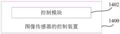
图14是本申请实施例的图像传感器的控制装置的示意框图;FIG14 is a schematic block diagram of a control device for an image sensor according to an embodiment of the present application;
图15是本申请实施例的电子设备的示意框图之一;FIG15 is a schematic block diagram of an electronic device according to an embodiment of the present application;
图16是本申请实施例的电子设备的示意框图之二。FIG. 16 is a second schematic block diagram of the electronic device according to an embodiment of the present application.
具体实施方式DETAILED DESCRIPTION
下面将结合本申请实施例中的附图,对本申请实施例中的技术方案进行清楚地描述,显然,所描述的实施例是本申请一部分实施例,而不是全部的实施例。基于本申请中的实施例,本领域普通技术人员获得的所有其他实施例,都属于本申请保护的范围。The following will be combined with the drawings in the embodiments of the present application to clearly describe the technical solutions in the embodiments of the present application. Obviously, the described embodiments are part of the embodiments of the present application, rather than all the embodiments. All other embodiments obtained by ordinary technicians in this field based on the embodiments in the present application belong to the scope of protection of this application.
本申请的说明书和权利要求书中的术语“第一”、“第二”等是用于区别类似的对象,而不用于描述特定的顺序或先后次序。应该理解这样使用的数据在适当情况下可以互换,以便本申请的实施例能够以除了在这里图示或描述的那些以外的顺序实施。此外,说明书以及权利要求中“和/或”表示所连接对象的至少其中之一,字符“/”,一般表示前后关联对象是一种“或”的关系。The terms "first", "second", etc. in the specification and claims of the present application are used to distinguish similar objects, and are not used to describe a specific order or precedence. It should be understood that the data used in this way can be interchanged under appropriate circumstances, so that the embodiments of the present application can be implemented in an order other than those illustrated or described here. In addition, the "and/or" in the specification and claims represents at least one of the connected objects, and the character "/" generally represents that the objects associated with each other are in an "or" relationship.
采用RGBW3.0的CIS的像素阵列(Pixel Array)是由像素团构成的。如图1所示,每一个像素团100拥有5个像素(Pixel),其中4个有色像素(即彩色像素),包括红色像素102、蓝色像素104和两个绿色像素106,均为“L”形状,而无色透明的白色像素108则仍为正方形,白色像素108位于像素团100的正中心,由4个“L”型的有色像素包裹环绕。在每一个有色像素的彩色滤光片下为感光元件,例如光电二极管,其作用为将彩色滤光片滤出的光线转换为用于后端处理的电学信号,例如电流、电压、电势能等。The pixel array of CIS using RGBW3.0 is composed of pixel clusters. As shown in FIG1 , each
而在现代的CIS制造工艺中,异形像素(即“L”型)由于其工艺和良率问题,目前仍然无法大规模应用在消费类CIS产品中。为了成功实践,RGBW3.0中的“L”型有色像素被拆分为多个矩形像素。如图2和图3所示,为两种方案。如图2所示,在方案1中,红区域202、蓝区域204、绿色区域206均由3个像素构成。而中间的白色区域208则由4个像素构成,每个像素的大小均一致。如图3所示,在方案2中,每个有色区域则由5个像素构成,而中心的白色区域208则由16个像素构成。不论上述何种方法,绿色像素,红色像素,蓝色像素的个数比值不变,始终为2:1:1。然而由于白色像素的个数变化,使得白色区域在像素团区域的占比改变,方法1中白色像素与有色像素的比值为1:3,方法2中白色像素与有色像素的比值为4:5。In modern CIS manufacturing processes, irregular pixels (i.e., "L"-shaped) are still not widely used in consumer CIS products due to their process and yield issues. In order to successfully implement, the "L"-shaped colored pixels in RGBW3.0 are split into multiple rectangular pixels. As shown in Figures 2 and 3, there are two solutions. As shown in Figure 2, in
采用RGBW3.0的CIS像素电路阵列架构如图4所示,每一行像素均共享一组像素控制信号,像素控制信号包括:像素重置信号


对于每一个像素,都包含了一个像素电路。如图4所示,像素电路404包括4晶体管有源像素感应(Active Pixel Sensor,APS)电路,其中感光的光电二极管(Photodiode,PD)将光线转换成电子后通过电荷转移晶体管(由

采用RGBW3.0 CFA后,由于其与拜耳RGB以及柯达RGBW等传统CFA形式相比,结构发生了较大改变,因此无法适用传统的像素阵列对应的像素信号处理电路。而本申请提供的图像传感器和电子设备即可解决上述问题。After adopting RGBW3.0 CFA, the structure has changed significantly compared with traditional CFA forms such as Bayer RGB and Kodak RGBW, so it cannot be used for pixel signal processing circuits corresponding to traditional pixel arrays. The image sensor and electronic device provided by this application can solve the above problems.
下面结合附图,通过具体的实施例及其应用场景对本申请实施例提供的图像传感器、控制方法、控制装置、电子设备和存储介质进行详细地说明。The image sensor, control method, control device, electronic device and storage medium provided in the embodiments of the present application are described in detail below with reference to the accompanying drawings through specific embodiments and their application scenarios.
本申请实施例提供了一种图像传感器,该图像传感器包括:An embodiment of the present application provides an image sensor, the image sensor comprising:
像素电路阵列,像素电路阵列包括多个像素团电路,每个像素团电路包括一个白色像素电路和至少两个彩色像素电路,至少两个彩色像素电路围绕白色像素电路设置,像素电路阵列包括至少两行像素电路行和至少两列像素电路列,至少两个像素电路行共用一个控制信号线,至少两个像素电路列共用一个输出信号线,其中,像素电路行包括白色像素电路或彩色像素电路,像素电路列包括白色像素电路或彩色像素电路;A pixel circuit array, wherein the pixel circuit array includes a plurality of pixel group circuits, each pixel group circuit includes a white pixel circuit and at least two color pixel circuits, the at least two color pixel circuits are arranged around the white pixel circuit, the pixel circuit array includes at least two rows of pixel circuits and at least two columns of pixel circuits, at least two rows of pixel circuits share a control signal line, and at least two columns of pixel circuits share an output signal line, wherein the pixel circuit rows include white pixel circuits or color pixel circuits, and the pixel circuit columns include white pixel circuits or color pixel circuits;
像素信号处理模块,像素信号处理模块与输出信号线相连接。The pixel signal processing module is connected to the output signal line.
在该实施例中,对于“L”型像素结构的方案,像素层的CFA采用了图1所示的布局,每个像素团包括4个彩色像素和1个白色像素,其中4个彩色像素包括红色像素(R)、蓝色像素(B)和两个绿色像素(G),均为“L”形状,而无色透明的白色像素(W)则为正方形,白色像素位于像素团的正中心,由4个“L”型的彩色像素包裹环绕。In this embodiment, for the "L" type pixel structure, the CFA of the pixel layer adopts the layout shown in Figure 1, and each pixel cluster includes 4 color pixels and 1 white pixel, wherein the 4 color pixels include a red pixel (R), a blue pixel (B) and two green pixels (G), all of which are "L" shaped, and the colorless and transparent white pixel (W) is a square. The white pixel is located in the center of the pixel cluster and is surrounded by 4 "L" shaped color pixels.
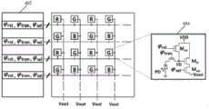
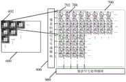
像素阵列600以及像素阵列600对应的像素电路阵列700的电路结构,如图5所示,像素电路阵列700由多个像素团电路702构成,一个像素团电路702由多个像素电路704构成(像素阵列600中的一个像素团602对应一个像素团电路604,像素阵列600中的一个像素对应一个像素电路704),每一行像素电路均由像素控制信号生成模块800进行控制。The circuit structure of the
像素电路行中包括白色像素电路或彩色像素电路,且像素电路列中包括白色像素电路或彩色像素电路,相当于,像素电路阵列的每个像素电路行共用一个控制信号线路,像素电路阵列的每个像素电路列共用一个输出信号线路,具体包括:每一行的彩色像素电路共用一个像素控制信号(也即控制信号线路),每一行的白色像素电路共用一个像素控制信号;每一列的彩色像素电路共用一个输出信号线,每一列的白色像素电路共用一个输出信号线。每一行白色像素电路共用的像素控制信号与每一行彩色像素电路共用的像素控制信号相互独立,彩色像素电路的输出信号线与白色像素电路的输出信号线相互独立。每一列彩色像素电路的输出电压信号为Vout,每一列白色像素电路输出的电压信号为Vout_w,信号传输线路将每列的输出信号(Vout和Vout_w)传输至像素信号处理模块900,由像素信号处理模块900进行处理。The pixel circuit row includes a white pixel circuit or a color pixel circuit, and the pixel circuit column includes a white pixel circuit or a color pixel circuit, which is equivalent to that each pixel circuit row of the pixel circuit array shares a control signal circuit, and each pixel circuit column of the pixel circuit array shares an output signal circuit, specifically including: the color pixel circuits of each row share a pixel control signal (that is, a control signal circuit), and the white pixel circuits of each row share a pixel control signal; the color pixel circuits of each column share an output signal line, and the white pixel circuits of each column share an output signal line. The pixel control signal shared by each row of white pixel circuits is independent of the pixel control signal shared by each row of color pixel circuits, and the output signal line of the color pixel circuit is independent of the output signal line of the white pixel circuit. The output voltage signal of each column of color pixel circuits is Vout , and the voltage signal output by each column of white pixel circuits is Vout_w . The signal transmission line transmits the output signal (Vout and Vout_w ) of each column to the pixel
本申请实施例提供了一种RGBW的像素电路阵列架构,相对于传统的像素电路阵列,实现了对像素电路阵列的重新布局。一方面,此像素电路阵列架构适用于CFA类型(例如,RGBW3.0 CFA),解决了CFA无法使用传统的像素电路阵列的问题,为CFA在CIS上的广泛应用提供基础;另一方面,实现了彩色像素与白色像素之间信号的独立处理,在适配采用CFA像素结构的同时,有效地避免了彩色像素与白色像素间信号的串扰,提高了图像传感器的灵敏度。The embodiment of the present application provides an RGBW pixel circuit array architecture, which realizes the rearrangement of the pixel circuit array relative to the traditional pixel circuit array. On the one hand, this pixel circuit array architecture is suitable for CFA type (for example, RGBW3.0 CFA), which solves the problem that CFA cannot use the traditional pixel circuit array, and provides a basis for the wide application of CFA on CIS; on the other hand, it realizes the independent processing of signals between color pixels and white pixels, and effectively avoids the crosstalk of signals between color pixels and white pixels while adapting to the CFA pixel structure, thereby improving the sensitivity of the image sensor.
进一步地,在本申请的一个实施例中,像素信号处理模块包括:多个选择模块,选择模块与第一输出信号线、第二输出信号线连接,其中第一输出信号线为白色像素电路列对应的输出信号线,第二输出信号线为与白色像素电路列相邻的一个彩色像素电路列对应的输出信号线,白色像素电路列为包括白色像素电路的像素电路列,彩色像素电路列为包括彩色像素电路的像素电路列;第一处理模块,第一处理模块包括:多个第一子处理模块,第一子处理模块与选择模块连接;以及多个第二子处理模块,第二子处理模块与第三输出信号线连接,第三输出信号线为与白色像素电路列相邻的另一个彩色像素电路列对应的输出信号线;第一处理缓存模块,与第一处理模块连接。Further, in one embodiment of the present application, the pixel signal processing module includes: a plurality of selection modules, the selection modules are connected to a first output signal line and a second output signal line, wherein the first output signal line is an output signal line corresponding to a white pixel circuit column, and the second output signal line is an output signal line corresponding to a color pixel circuit column adjacent to the white pixel circuit column, the white pixel circuit column is a pixel circuit column including white pixel circuits, and the color pixel circuit column is a pixel circuit column including color pixel circuits; a first processing module, the first processing module includes: a plurality of first sub-processing modules, the first sub-processing module is connected to the selection module; and a plurality of second sub-processing modules, the second sub-processing module is connected to a third output signal line, and the third output signal line is an output signal line corresponding to another color pixel circuit column adjacent to the white pixel circuit column; a first processing cache module, connected to the first processing module.
其中,选择模块将第一输出信号线的第一输出信号或第二输出信号线的第二输出信号传输至第一子处理模块,第一子处理模块对第一输出信号或第二输出信号进行放大处理,以及对放大处理后的第一输出信号或第二输出信号进行模数转换处理;第二子处理模块用于对第三输出信号线的第三输出信号进行放大处理,以及对放大处理后的第三输出信号进行模数转换处理。第一处理缓存模块用于对第一输出信号、第二输出信号和第三输出信号进行存储,并对存储的第一输出信号、第二输出信号和第三输出信号进行图像处理,以提高第一输出信号、第二输出信号和第三输出信号的信号质量,图像处理具体包括线性纠正、坏点去除、内插、白平衡、自动曝光控制等后期处理。Among them, the selection module transmits the first output signal of the first output signal line or the second output signal of the second output signal line to the first sub-processing module, the first sub-processing module amplifies the first output signal or the second output signal, and performs analog-to-digital conversion on the amplified first output signal or the second output signal; the second sub-processing module is used to amplify the third output signal of the third output signal line, and perform analog-to-digital conversion on the amplified third output signal. The first processing cache module is used to store the first output signal, the second output signal and the third output signal, and perform image processing on the stored first output signal, the second output signal and the third output signal to improve the signal quality of the first output signal, the second output signal and the third output signal, and the image processing specifically includes post-processing such as linear correction, bad pixel removal, interpolation, white balance, and automatic exposure control.
在该实施例中,像素信号处理模块包括多个选择模块、第一处理模块以及第一处理缓存模块,第一处理模块包括多个第一子处理模块和多个第二子处理模块。白色像素电路列对应的输出信号线(即第一输出信号线)的输出信号和与其相邻的一个彩色像素电路列对应的输出信号线(即第二输出信号线)的输出信号,通过一个选择模块复用同一个第一子处理模块。而与第一输出信号线相邻的另一个彩色像素电路列对应的输出信号线(即第三输出信号线)的输出信号使用第二子处理模块。In this embodiment, the pixel signal processing module includes a plurality of selection modules, a first processing module and a first processing buffer module, and the first processing module includes a plurality of first sub-processing modules and a plurality of second sub-processing modules. The output signal of the output signal line corresponding to the white pixel circuit column (i.e., the first output signal line) and the output signal of the output signal line corresponding to a color pixel circuit column adjacent thereto (i.e., the second output signal line) are multiplexed in the same first sub-processing module through a selection module. The output signal of the output signal line corresponding to another color pixel circuit column adjacent to the first output signal line (i.e., the third output signal line) uses the second sub-processing module.
第一处理缓存模块与所有的第一子处理模块、所有的第二子处理模块连接,用于对进行放大处理和模数转换处理后的第一输出信号、第二输出信号和第三输出信号依次进行存储和图像处理。The first processing buffer module is connected to all the first sub-processing modules and all the second sub-processing modules, and is used to sequentially store and image-process the first output signal, the second output signal and the third output signal after amplification processing and analog-to-digital conversion processing.
示例性地,如图6所示,像素信号处理模块900包括模拟数据选择器(Analog DataMultiplexer,MUX)902、第一子处理模块904、第二子处理模块906以及第一处理缓存模块908。每一列彩色像素电路7042的输出信号为Vout、每一列白色像素电路7044的输出信号为Vout_w,一个输出信号Vout和一个输出信号Vout_w通过一个MUX 902后,复用一个第一子处理模块904,其中,MUX即为上述选择模块,第一子处理模块904包括一个可调增益放大器(Programmable Gain Amplifier,PGA)电路9042和一个模数转换器(Analog-to-DigitalConvertor,ADC)电路9044,第二子处理模块906包括一个PGA电路9062和一个ADC电路9064。PGA电路用于对信号进行放大处理,其输出的信号VPGA再输入至ADC电路,ADC电路用于对信号VPGA进行模数转换处理。第一处理缓存模块908即为ISP和图像缓存器,用于对信号进行存储和图像处理。Exemplarily, as shown in FIG6 , the pixel
需要说明的是,如图6所示,MUX902的两个输入信号分别为一列像素团电路中的一个白色像素电路列的输出信号Vout_w,以及该列像素团电路中的任一个彩色像素电路列的输出信号Vout。It should be noted that, as shown in FIG. 6 , the two input signals of
在按照逐行扫描的方式读取像素电路的信号的情况下,首先读取第一行像素,例如读取彩色像素R的信号和彩色像素G的信号,彩色像素R的信号传输至MUX 902中,再传输至PGA电路、ADC电路中进行处理,彩色像素G的信号直接传输至PGA电路、ADC电路中进行处理。然后读取第二行像素,例如读取白色像素W的信号,白色像素W的信号传输至MUX902中,再传输至PGA电路、ADC电路,且与彩色像素R的信号共用的相同的PGA电路、ADC电路。由于第一行像素和第二行像素不同时读取,所以不会出现PGA电路、ADC电路的处理冲突。When the signal of the pixel circuit is read in a row-by-row scanning manner, the first row of pixels is read first, for example, the signal of the color pixel R and the signal of the color pixel G are read, the signal of the color pixel R is transmitted to MUX 902, and then transmitted to the PGA circuit and the ADC circuit for processing, and the signal of the color pixel G is directly transmitted to the PGA circuit and the ADC circuit for processing. Then the second row of pixels is read, for example, the signal of the white pixel W is read, the signal of the white pixel W is transmitted to MUX 902, and then transmitted to the PGA circuit and the ADC circuit, and the same PGA circuit and ADC circuit are shared with the signal of the color pixel R. Since the first row of pixels and the second row of pixels are not read at the same time, there will be no processing conflict between the PGA circuit and the ADC circuit.
本申请的实施例中,由于白色像素与彩色像素的数量不同且在不同横行,因此白色像素的信号处理链路与彩色像素处理链路有部分子模块可以复用,从而节省空间和能耗。In the embodiment of the present application, since the number of white pixels and the color pixels are different and in different rows, some submodules of the white pixel signal processing link and the color pixel processing link can be reused, thereby saving space and energy consumption.
进一步地,在本申请的一个实施例中,第一处理缓存模块包括:多个第一分用模块,第一分用模块与第一子处理模块连接;多个第一缓存模块,第一缓存模块与第一分用模块连接;多个第二缓存模块,第二缓存模块与第一分用模块连接或者第二缓存模块与第二子处理模块连接;第一图像处理模块,与第一缓存模块和第二缓存模块连接。Further, in one embodiment of the present application, the first processing cache module includes: multiple first de-sharing modules, the first de-sharing module is connected to the first sub-processing module; multiple first cache modules, the first cache module is connected to the first de-sharing module; multiple second cache modules, the second cache module is connected to the first de-sharing module or the second cache module is connected to the second sub-processing module; a first image processing module, connected to the first cache module and the second cache module.
其中,第一缓存模块,用于对第一输出信号进行存储,第二缓存模块在与第一分用模块连接的情况下,用于对第二输出信号进行存储,第二缓存模块在与第二子处理模块连接的情况下,用于对第三输出信号进行存储,第一图像处理模块,用于对第一输出信号、第二输出信号和第三输出信号进行图像处理。Among them, the first cache module is used to store the first output signal, the second cache module is used to store the second output signal when connected to the first sharing module, the second cache module is used to store the third output signal when connected to the second sub-processing module, and the first image processing module is used to perform image processing on the first output signal, the second output signal and the third output signal.
在该实施例中,第一处理缓存模块包括多个第一分用模块、多个第一缓存模块、多个第二缓存模块以及第一图像处理模块。第一分用模块用于将第一子处理模块输出的第一输出信号和第二输出信号分别传输至不同的缓存模块。具体地,第一输出信号传输至第一缓存模块,第二输出信号传输至第二缓存模块,第三输出信号传输至第二缓存模块,也就是说,第一缓存模块中存储白色像素电路列的输出信号,第二缓存模块中存储彩色像素电路列的输出信号。In this embodiment, the first processing cache module includes a plurality of first demultiplexing modules, a plurality of first cache modules, a plurality of second cache modules and a first image processing module. The first demultiplexing module is used to transmit the first output signal and the second output signal output by the first sub-processing module to different cache modules respectively. Specifically, the first output signal is transmitted to the first cache module, the second output signal is transmitted to the second cache module, and the third output signal is transmitted to the second cache module, that is, the output signal of the white pixel circuit column is stored in the first cache module, and the output signal of the color pixel circuit column is stored in the second cache module.
第一图像处理模块再对第一缓存模块和第二缓存模块内存储的信号进行图像处理。The first image processing module then performs image processing on the signals stored in the first buffer module and the second buffer module.
需要说明的是,多个第一分用模块的数量与选择模块的数量相等。It should be noted that the number of the plurality of first demultiplexing modules is equal to the number of the selection modules.
示例性地,如图6所示,在进入第一处理缓存模块908后,通过第一处理缓存模块908的数字数据分用器(Digital Data Demultiplexer,DEMUX)9082将第一输出信号和第二输出信号存储至不同的缓存模块(Buffer和Buffer_W),DEMUX即为上述第一分用模块。具体地,第二输出信号和第三输出信号(即彩色像素列的输出信号)缓存在Buffer,而第一输出信号(即白色像素列的输出信号)缓存在Buffer_W。缓存后的信号进而进入ISP 9084进行数字图像处理相关的步骤。Exemplarily, as shown in FIG6 , after entering the first
通过上述方式,对彩色像素列的输出信号和白色像素列的输出信号进行了独立的缓存,第一图像处理模块可以任意地点选彩色像素列的输出信号或白色像素列的输出信号进行后期处理,极大的丰富了图像信号处理种类。Through the above method, the output signals of the color pixel columns and the output signals of the white pixel columns are cached independently, and the first image processing module can arbitrarily select the output signals of the color pixel columns or the output signals of the white pixel columns for post-processing, which greatly enriches the types of image signal processing.
需要说明的是,DEMUX 9082的电路结构如图8所示,DEMUX 9082由
常见的缓存模块有动态随机存取存储器(Dynamic Random AccessMemory,DRAM)、静态随机存取存储器(Static Random Access Memory,SRAM)等。Common cache modules include dynamic random access memory (DRAM), static random access memory (SRAM), etc.
图6中数据分用器也可放在ADC前,此时数据分用器则必须使用模拟数据分用器而非数字数据分用器。The data demultiplexer in FIG6 may also be placed before the ADC. In this case, the data demultiplexer must be an analog data demultiplexer rather than a digital data demultiplexer.
进一步地,在本申请的一个实施例中,像素信号处理模块还包括:多个第一采样模块,第一采样模块与输出信号线的输出端相连接。Furthermore, in one embodiment of the present application, the pixel signal processing module further includes: a plurality of first sampling modules, and the first sampling modules are connected to the output end of the output signal line.
第一采样模块用于对输出信号线的输出信号进行消噪音处理。The first sampling module is used to perform noise elimination processing on the output signal of the output signal line.
在该实施例中,像素信号处理模块还包括多个第一采样模块,第一采样模块的一端与输出信号线的输出端相连接,第一采样模块的另一端与选择模块或第二子处理模块相连接,第一采样模块用于对输出信号线的输出信号进行消噪音处理。In this embodiment, the pixel signal processing module also includes multiple first sampling modules, one end of the first sampling module is connected to the output end of the output signal line, and the other end of the first sampling module is connected to the selection module or the second sub-processing module. The first sampling module is used to perform noise elimination on the output signal of the output signal line.
示例性地,如图6所示,每一列彩色像素电路的输出信号为Vout、每一列白色像素电路的输出信号为Vout_w,输出信号Vout和输出信号Vout_w均通过独立的相关双采样(Corrolated Double Sampling,CDS)电路910(即第一采样模块)进行消噪音处理。具体地,通过两次采样(采样信号存储在电容C1与电容C2),使用运算放大器ACDS进行信号减法得到两次采样信号的差值,即VCDS信号。CDS电路910输出的VCDS信号会输入至PGA电路进行可调信号放大操作。Exemplarily, as shown in FIG6 , the output signal of each column of color pixel circuits is Vout , and the output signal of each column of white pixel circuits is Vout_w . The output signal Vout and the output signal Vout_w are both subjected to noise elimination processing by an independent Corrolated Double Sampling (CDS) circuit 910 (i.e., the first sampling module). Specifically, after two samplings (the sampling signals are stored in capacitors C1 and C2 ), an operational amplifier ACDS is used to perform signal subtraction to obtain the difference between the two sampling signals, i.e., the VCDS signal. The VCDS signal output by the
如图7所示,MUX包括开启S1、开关S2以及运算放大器,MUX由
通过上述方式,实现对彩色像素电路列的输出信号和白色像素电路列的输出信号进行消噪音处理,提高信号的准确性。By means of the above method, noise elimination processing is performed on the output signals of the color pixel circuit column and the output signals of the white pixel circuit column, thereby improving the accuracy of the signals.
需要说明的是,如图6所示,在像素信号处理模块900中每一条像素信号处理链路上的子模块均需要由信号处理&控制信号模块912提供时序与控制信号。当像素信号走完所有链路上子模块且缓存至Buffer或Buffer_W上后,信号将进入ISP 9084进行数字图像处理相关的步骤。处理完成后由I/O 914输出最后的图像信号至CIS芯片外。It should be noted that, as shown in FIG6 , each submodule on a pixel signal processing link in the pixel
进一步地,在本申请的一个实施例中,在白色像素电路包括多个子白色像素电路、彩色像素电路包括多个子彩色像素电路的情况下,像素电路行包括子彩色像素电路,或包括子白色像素电路和子彩色像素电路;像素电路列包括子彩色像素电路,或包括子白色像素电路和子彩色像素电路。Further, in one embodiment of the present application, when the white pixel circuit includes multiple sub-white pixel circuits and the color pixel circuit includes multiple sub-color pixel circuits, the pixel circuit row includes a sub-color pixel circuit, or includes a sub-white pixel circuit and a sub-color pixel circuit; the pixel circuit column includes a sub-color pixel circuit, or includes a sub-white pixel circuit and a sub-color pixel circuit.
在该实施例中,对于将白色像素拆分为多个矩形子白色像素、将彩色像素拆分为多个矩形子彩色像素的合成像素方案(如图2和图3所示)。以如图2中所示的结构为例,像素阵列600的每个像素团602中含有16个子像素,因此如图9所示,像素电路阵列700的每个像素团电路702中含有16个子像素电路706,具体为4个子白色像素电路和12个子彩色像素电路。每一行子像素电路均由像素控制信号生成模块800进行控制,每一列子像素电路的输出信号传输至像素信号处理模块900,由像素信号处理模块900进行处理。In this embodiment, for a synthetic pixel scheme in which a white pixel is split into a plurality of rectangular sub-white pixels and a color pixel is split into a plurality of rectangular sub-color pixels (as shown in FIG. 2 and FIG. 3 ), taking the structure shown in FIG. 2 as an example, each
像素电路阵列中,每一行中的子像素电路包括两种情况,一种为每一行中仅包括子彩色像素电路,另一种为每一行中包括子白色像素电路和子彩色像素电路;每一列中的子像素电路包括两种情况,一种为每一列中仅包括子彩色像素电路,另一种为每一列中包括子白色像素电路和子彩色像素电路。In the pixel circuit array, the sub-pixel circuits in each row include two cases, one is that each row includes only sub-color pixel circuits, and the other is that each row includes sub-white pixel circuits and sub-color pixel circuits; the sub-pixel circuits in each column include two cases, one is that each column includes only sub-color pixel circuits, and the other is that each column includes sub-white pixel circuits and sub-color pixel circuits.
每一行的所有子像素电路(不论是子彩色像素电路还是子白色像素电路)均由像素控制信号生成模块进行控制,也即,每一行的所有子像素电路共用一个像素控制信号(也即控制信号线)。每一列的所有子像素电路(不论是子彩色像素电路还是子白色像素电路)输出的信号共用一条信号传输线路(也即输出信号线)至像素信号处理模块。All sub-pixel circuits in each row (whether they are sub-color pixel circuits or sub-white pixel circuits) are controlled by the pixel control signal generation module, that is, all sub-pixel circuits in each row share a pixel control signal (that is, a control signal line). The signals output by all sub-pixel circuits in each column (whether they are sub-color pixel circuits or sub-white pixel circuits) share a signal transmission line (that is, an output signal line) to the pixel signal processing module.
本申请实施例提供了一种RGBW的像素电路阵列架构,一方面,此像素电路阵列架构适用于CFA类型(例如,RGBW3.0 CFA)的合成像素方案,解决了CFA的合成像素方案无法使用传统的像素电路阵列的问题,为CFA在CIS上的广泛应用提供基础;另一方面,像素电路阵列中每一个像素电路均可进行信号处理与读出,在适配采用CFA像素结构的同时,有效地避免了像素间信号的串扰。The embodiment of the present application provides an RGBW pixel circuit array architecture. On the one hand, this pixel circuit array architecture is suitable for a synthetic pixel solution of the CFA type (for example, RGBW3.0 CFA), which solves the problem that the synthetic pixel solution of CFA cannot use a traditional pixel circuit array, and provides a basis for the widespread application of CFA on CIS; on the other hand, each pixel circuit in the pixel circuit array can perform signal processing and readout, which effectively avoids crosstalk of signals between pixels while adapting to the CFA pixel structure.
进一步地,在本申请的一个实施例中,像素信号处理模块包括:多个第二处理模块,第二处理模块与输出信号线连接;第二处理缓存模块,第二处理缓存模块包括:多个第二分用模块,第二分用模块与第一目标处理模块连接,其中第一目标处理模块为与第一目标像素电路列对应的输出信号线相连接的第二处理模块,第一目标像素电路列为包括子白色像素电路和子彩色像素电路的像素电路列;多个第三缓存模块,第三缓存模块与第二分用模块连接;多个第四缓存模块,第四缓存模块与第二分用模块连接,或第四缓存模块与第二目标处理模块连接,第二目标处理模块为与第二目标像素电路列对应的输出信号线相连接的第二处理模块,第二目标像素电路列为包括子彩色像素电路的像素电路列;以及第二图像处理模块,与第三缓存模块和第四缓存模块连接。Further, in one embodiment of the present application, the pixel signal processing module includes: a plurality of second processing modules, the second processing modules are connected to the output signal line; a second processing cache module, the second processing cache module includes: a plurality of second de-using modules, the second de-using module is connected to the first target processing module, wherein the first target processing module is a second processing module connected to the output signal line corresponding to the first target pixel circuit column, and the first target pixel circuit column is a pixel circuit column including a sub-white pixel circuit and a sub-color pixel circuit; a plurality of third cache modules, the third cache module is connected to the second de-using module; a plurality of fourth cache modules, the fourth cache module is connected to the second de-using module, or the fourth cache module is connected to the second target processing module, the second target processing module is a second processing module connected to the output signal line corresponding to the second target pixel circuit column, and the second target pixel circuit column is a pixel circuit column including a sub-color pixel circuit; and a second image processing module, connected to the third cache module and the fourth cache module.
其中,第二处理模块,用于对输出信号线的输出信号进行放大处理,并对进行放大处理后的输出信号进行模数转换处理;第三缓存模块,用于对第四输出信号进行存储,第四输出信号为第一目标像素电路列对应的输出信号线输出的子白色像素电路的信号;第四缓存模块在与第二分用模块连接的情况下,用于对第五输出信号进行存储,第五输出信号为第一目标像素电路列对应的输出信号线输出的子彩色像素电路的信号,第四缓存模块在与第二目标处理模块连接的情况下,用于对第二目标处理模块的第六输出信号进行存储;第二图像处理模块,用于对第四输出信号、第五输出信号和第六输出信号进行图像处理,以提高第四输出信号、第五输出信号和第六输出信号的信号质量,图像处理具体包括线性纠正、坏点去除、内插、白平衡、自动曝光控制等后期处理。Among them, the second processing module is used to amplify the output signal of the output signal line and perform analog-to-digital conversion on the amplified output signal; the third cache module is used to store the fourth output signal, which is the signal of the sub-white pixel circuit output by the output signal line corresponding to the first target pixel circuit column; the fourth cache module is used to store the fifth output signal when connected to the second de-sharing module, which is the signal of the sub-color pixel circuit output by the output signal line corresponding to the first target pixel circuit column; the fourth cache module is used to store the sixth output signal of the second target processing module when connected to the second target processing module; the second image processing module is used to perform image processing on the fourth output signal, the fifth output signal and the sixth output signal to improve the signal quality of the fourth output signal, the fifth output signal and the sixth output signal, and the image processing specifically includes post-processing such as linear correction, bad pixel removal, interpolation, white balance, and automatic exposure control.
在该实施例中,对于合成像素方案,像素信号处理模块包括多个第二处理模块和一个第二处理缓存模块,第二处理缓存模块包括多个第二分用模块、多个第三缓存模块、多个第四缓存模块和一个第二图像处理模块。第二处理模块用于对输出信号线的输出信号进行放大处理和模数转换处理,第二分用模块将进行了放大处理和模数转换处理后的第一目标像素电路列的输出信号分别传输至不同的缓存模块(即第三缓存模块和第四缓存模块)中进行存储。具体地,第一目标像素电路列的输出信号包括子白色像素电路的信号(即第四输出信号)和子彩像素电路的信号(即第五输出信号),利用第二分用模块将第四输出信号传输至第三缓存模块进行存储,利用第二分用模块将第五输出信号传输至第四缓存模块进行存储。In this embodiment, for the synthetic pixel scheme, the pixel signal processing module includes a plurality of second processing modules and a second processing buffer module, and the second processing buffer module includes a plurality of second demultiplexing modules, a plurality of third buffer modules, a plurality of fourth buffer modules and a second image processing module. The second processing module is used to amplify and perform analog-to-digital conversion on the output signal of the output signal line, and the second demultiplexing module transmits the output signal of the first target pixel circuit column after the amplification and analog-to-digital conversion to different buffer modules (i.e., the third buffer module and the fourth buffer module) for storage. Specifically, the output signal of the first target pixel circuit column includes the signal of the sub-white pixel circuit (i.e., the fourth output signal) and the signal of the sub-color pixel circuit (i.e., the fifth output signal), and the fourth output signal is transmitted to the third buffer module for storage by the second demultiplexing module, and the fifth output signal is transmitted to the fourth buffer module for storage by the second demultiplexing module.
另外,第二目标像素电路列的输出信号仅包括子彩色像素电路的信号(即第六输出信号),则将第二目标像素电路列的输出信号在利用第二目标处理模块进行放大处理和模数转换处理后,直接传输至第四缓存模块进行存储。In addition, the output signal of the second target pixel circuit column only includes the signal of the sub-color pixel circuit (i.e., the sixth output signal). The output signal of the second target pixel circuit column is directly transmitted to the fourth cache module for storage after being amplified and analog-to-digital converted by the second target processing module.
第二图像处理模块再对第三缓存模块和第四缓存模块内存储的信号进行图像处理。The second image processing module then performs image processing on the signals stored in the third buffer module and the fourth buffer module.
其中,第一目标处理模块和第二目标处理模块均包括一个PGA电路和一个ADC电路。PGA电路用于对信号进行放大处理,其输出的信号VPGA或信号VPGA/W再输入至ADC电路,ADC电路用于对信号VPGA或信号VPGA/W进行模数转换处理。The first target processing module and the second target processing module each include a PGA circuit and an ADC circuit. The PGA circuit is used to amplify the signal, and the output signal VPGA or signal VPGA/W is then input to the ADC circuit, and the ADC circuit is used to perform analog-to-digital conversion on the signal VPGA or signal VPGA/W .
示例性地,如图10所示,像素信号处理模块900包括第一目标处理模块916、第二目标处理模块918以及第二处理缓存模块920。每一个子彩色像素电路列的输出信号为Vout、每一个包括子白色像素电路和子彩色像素电路的像素电路列的输出信号为Vout/w,输出信号Vout通过第二目标处理模块918,输出信号Vout/w通过第一目标处理模块916,进入ISP和图像缓存器(即第二处理缓存模块920)。第一目标处理模块916包括一个PGA电路9162和一个ADC电路9164,第二目标处理模块918包括一个PGA电路9182和一个ADC电路9184。Exemplarily, as shown in FIG10 , the pixel
由于在一个像素团中,子白色像素只存在于中间两列,因此在有子白色像素存在的列链路上设置一个DEMUX 9202,在输出信号Vout/w通过DEMUX9202后,将子彩色像素信息(即上述第五输出信号)与子白色像素信息(即上述第四输出信号)分别缓存至对不同的缓存模块(Buffer或Buffer_W)。具体地,第五输出信号缓存在Buffer,而第四输出信号缓存在Buffer_W。另外,仅包括子彩色像素电路的像素电路列的输出信号Vout(即上述第六输出信号)缓存在Buffer。Since in a pixel cluster, sub-white pixels only exist in the middle two columns, a
在按照逐行扫描的方式读取像素电路的信号的情况下,首先读取第一行像素,例如读取子彩色像素R1、R2、G1、G2的信号,子彩色像素R1、G2的信号传输至对应的PGA电路、ADC电路后,再存储至对应的Buffer,子彩色像素R2、G1的信号传输至对应的PGA电路、ADC电路后,被DEMUX分配至对应的Buffer中进行存储。然后读取第二行像素,例如读取子彩色像素R3、G3的信号以及子白色像素W1、W2的信号,子彩色像素R3、G3的信号传输至对应的PGA电路、ADC电路后,再存储至对应的Buffer,子白色像素W1、W2的信号传输至对应的PGA电路、ADC电路后,被DEMUX分配至对应的Buffer_W中进行存储。When the signals of the pixel circuit are read in a row-by-row scanning manner, the first row of pixels is read first, for example, the signals of the sub-color pixels R1 , R2 , G1 , and G2 are read. After the signals of the sub-color pixels R1 , G2 are transmitted to the corresponding PGA circuit and ADC circuit, they are stored in the corresponding Buffer. After the signals of the sub-color pixels R2 , G1 are transmitted to the corresponding PGA circuit and ADC circuit, they are allocated by DEMUX to the corresponding Buffer for storage. Then the second row of pixels is read, for example, the signals of the sub-color pixels R3 , G3 and the signals of the sub-white pixels W1 , W2 are read. After the signals of the sub-color pixels R3 , G3 are transmitted to the corresponding PGA circuit and ADC circuit, they are stored in the corresponding Buffer. After the signals of the sub-white pixels W1 , W2 are transmitted to the corresponding PGA circuit and ADC circuit, they are allocated by DEMUX to the corresponding Buffer_W for storage.
通过上述方式,像素信号处理模块适配采用合成像素方案的像素阵列,通过使用不同的缓存模块将子彩色像素电路的信号与子白色像素电路的信号进行独立缓存,避免了信号之间的混乱与杂揉,为ISP进行后期处理提供了方便。Through the above method, the pixel signal processing module adapts to the pixel array using the synthetic pixel solution. By using different cache modules to independently cache the signals of the sub-color pixel circuit and the sub-white pixel circuit, confusion and mixing between the signals are avoided, which provides convenience for ISP to perform post-processing.
需要说明的是,常见的缓存模块有DRAM、SRAM等。DEMUX的电路结构如图8所示。图10中数据分用器也可放在ADC前,此时数据分用器则必须使用模拟数据分用器而非数字数据分用器。It should be noted that common cache modules include DRAM, SRAM, etc. The circuit structure of DEMUX is shown in Figure 8. The data demultiplexer in Figure 10 can also be placed before the ADC. In this case, the data demultiplexer must use an analog data demultiplexer instead of a digital data demultiplexer.
进一步地,在本申请的一个实施例中,第二处理缓存模块还包括:多个信号合成模块,信号合成模块与第二图像处理模块、第一目标缓存模块和第二目标缓存模块相连接,第一目标缓存模块和第二目标缓存模块为分别存储目标像素团电路中相邻行的两个子白色像素电路的信号的第三缓存模块。Furthermore, in one embodiment of the present application, the second processing cache module also includes: multiple signal synthesis modules, the signal synthesis module is connected to the second image processing module, the first target cache module and the second target cache module, the first target cache module and the second target cache module are third cache modules that respectively store signals of two sub-white pixel circuits in adjacent rows in the target pixel group circuit.
其中,信号合成模块用于将第一目标缓存模块的输出信号和第二目标缓存模块的输出信号进行融合,也即增强第一目标缓存模块的输出信号和第二目标缓存模块的输出信号。The signal synthesis module is used to fuse the output signal of the first target buffer module and the output signal of the second target buffer module, that is, to enhance the output signal of the first target buffer module and the output signal of the second target buffer module.
在该实施例中,由于合成像素方案,可能需要进行同色像素信号融合的情况,子彩色像素的同色像素合成一般发生在像素阵列中,而子白色像素的信号合成则在像素阵列中较难实现。In this embodiment, due to the synthetic pixel scheme, same-color pixel signal fusion may be required. The same-color pixel synthesis of sub-color pixels generally occurs in the pixel array, while the signal synthesis of sub-white pixels is more difficult to achieve in the pixel array.
对此,本申请实施例提供了子白色像素的信号融合方案,在采用了子彩色像素信号融合的情况下,利用信号合成模块使对应的子白色像素信号进行信号融合。具体地,第二处理缓存模块包括多个信号合成模块,信号合成模块用于目标像素团电路中相邻行的两个子白色像素电路的信号,而相邻行的两个子白色像素电路的信号是分别存储在第一目标缓存模块和第二目标缓存模块中的信号,目标像素团电路为像素电路阵列中的任一个像素团电路。In this regard, the embodiment of the present application provides a signal fusion solution for sub-white pixels. When sub-color pixel signal fusion is adopted, a signal synthesis module is used to perform signal fusion on the corresponding sub-white pixel signals. Specifically, the second processing cache module includes a plurality of signal synthesis modules, and the signal synthesis module is used for the signals of two sub-white pixel circuits in adjacent rows in the target pixel group circuit, and the signals of the two sub-white pixel circuits in adjacent rows are signals stored in the first target cache module and the second target cache module respectively, and the target pixel group circuit is any pixel group circuit in the pixel circuit array.
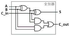
示例性地,如图10所示,在两个相邻的Buffer_W的输出端设置一个加法器9206(即上述信号合成模块),即可轻易地实现子白色像素(例如,子白色像素W1和子白色像素W2,或者子白色像素W3和子白色像素W4)的信号融合。需要说明的是,如图10所示,由于加法器9206是在ADC后,因此是进行数字信号合成。Exemplarily, as shown in FIG10 , an adder 9206 (i.e., the above-mentioned signal synthesis module) is provided at the output end of two adjacent Buffer_W, so that the signal fusion of the sub-white pixels (e.g., the sub-white pixel W1 and the sub-white pixel W2 , or the sub-white pixel W3 and the sub-white pixel W4 ) can be easily realized. It should be noted that, as shown in FIG10 , since the
加法器的电路结构如图11所示,加法器有多个全加器构成,全加器的的电路结构如图12所示。N位二进制数字信号A1、A2、……、AN与N位二进制数字信号B1、B2、……、BN在通过加法器后将分别生成N位二进制数字信号S1、S2、……、SN。C1、C2、……、CN为加法中的进位。The circuit structure of the adder is shown in FIG11 . The adder is composed of a plurality of full adders, and the circuit structure of the full adder is shown in FIG12 . N-bit binary digital signals A1 , A2 , …,AN and N-bit binary digital signals B1 , B2 , …,BN will generate N-bit binary digital signals S1 , S2 , …,SN respectively after passing through the adder. C1 , C2 , …,CN are the carries in the addition.
通过上述方式,实现相邻的两个子白色像素信号的融合,为ISP进行后期处理提供了方便。Through the above method, the fusion of two adjacent sub-white pixel signals is achieved, which provides convenience for ISP to perform post-processing.
进一步地,在本申请的一个实施例中,像素信号处理模块还包括:多个第二采样模块,第二采样模块连接于第二处理模块与输出信号线之间。其中,第二采样模块用于对输出信号线的输出信号进行消噪音处理。Furthermore, in one embodiment of the present application, the pixel signal processing module further includes: a plurality of second sampling modules, the second sampling modules being connected between the second processing module and the output signal line, wherein the second sampling modules are used to perform noise elimination processing on the output signal of the output signal line.
在该实施例中,像素信号处理模块还包括多个第二采样模块,第二采样模块的一端与输出信号线的输出端相连接,第二采样模块的另一端与第二处理模块相连接,第二采样模块用于对输出信号线的输出信号进行消噪音处理。In this embodiment, the pixel signal processing module also includes multiple second sampling modules, one end of the second sampling module is connected to the output end of the output signal line, and the other end of the second sampling module is connected to the second processing module. The second sampling module is used to perform noise elimination on the output signal of the output signal line.
示例性地,如图10所示,每一个仅包括子彩色像素电路的像素电路列的输出信号为Vout、每一个包括子彩色像素电路和子白色像素电路的像素电路列的输出信号为Vout/w,输出信号Vout和输出信号Vout/w均通过独立的CDS 922(即第二采样模块)进行消噪音处理。Exemplarily, as shown in FIG10 , the output signal of each pixel circuit column including only sub-color pixel circuits is Vout , and the output signal of each pixel circuit column including sub-color pixel circuits and sub-white pixel circuits is Vout/w , and both the output signal Vout and the output signal Vout/w are subjected to noise elimination processing by an independent CDS 922 (i.e., the second sampling module).
通过上述方式,实现对输出信号线的输出信号进行消噪音处理,提高信号的准确性。Through the above method, the output signal of the output signal line is de-noised, thereby improving the accuracy of the signal.
需要说明的是,如图10所示,在像素信号处理模块中每一条像素信号处理链路上的子模块均需要由信号处理&控制信号模块912提供时序与控制信号。当像素信号走完所有链路上子模块且缓存至Buffer或Buffer_W上后,信号将进入ISP 9204进行数字图像处理相关的步骤。处理完成后由I/O914输出最后的图像信号至CIS芯片外。It should be noted that, as shown in FIG10 , each submodule on a pixel signal processing link in the pixel signal processing module needs to be provided with timing and control signals by the signal processing &
本申请实施例提供了一种电子设备,该电子设备包括如上述实施例的图像传感器。An embodiment of the present application provides an electronic device, which includes an image sensor as described in the above embodiment.
在该实施例中,图像传感器的像素电路阵列由多个像素团电路构成。像素电路阵列的每个像素电路行共用一个控制信号线路,像素电路阵列的每个像素电路列共用一个输出信号线路,具体包括:每一行的彩色像素电路共用一个控制信号线,每一行的白色像素电路共用一个像素控制信号;每一列的彩色像素电路共用一个输出信号线,每一列的白色像素电路共用一个输出信号线。每一行白色像素电路共用的像素控制信号与每一行彩色像素电路共用的像素控制信号相互独立,彩色像素电路的输出信号线与白色像素电路的输出信号线相互独立。In this embodiment, the pixel circuit array of the image sensor is composed of a plurality of pixel group circuits. Each pixel circuit row of the pixel circuit array shares a control signal line, and each pixel circuit column of the pixel circuit array shares an output signal line, specifically including: each row of color pixel circuits shares a control signal line, and each row of white pixel circuits shares a pixel control signal; each column of color pixel circuits shares an output signal line, and each column of white pixel circuits shares an output signal line. The pixel control signal shared by each row of white pixel circuits is independent of the pixel control signal shared by each row of color pixel circuits, and the output signal line of the color pixel circuit is independent of the output signal line of the white pixel circuit.
本申请实施例提供了一种RGBW的像素电路阵列架构,相对于传统的像素电路阵列,实现了对像素电路阵列的重新布局。一方面,此像素电路阵列架构适用于CFA类型(例如,RGBW3.0 CFA),解决了CFA无法使用传统的像素电路阵列的问题,为CFA在CIS上的广泛应用提供基础;另一方面,实现了彩色像素与白色像素之间信号的独立处理,在适配采用CFA像素结构的同时,有效地避免了彩色像素与白色像素间信号的串扰,提高了图像传感器的灵敏度。The embodiment of the present application provides an RGBW pixel circuit array architecture, which realizes the rearrangement of the pixel circuit array relative to the traditional pixel circuit array. On the one hand, this pixel circuit array architecture is suitable for CFA type (for example, RGBW3.0 CFA), which solves the problem that CFA cannot use the traditional pixel circuit array, and provides a basis for the wide application of CFA on CIS; on the other hand, it realizes the independent processing of signals between color pixels and white pixels, and effectively avoids the crosstalk of signals between color pixels and white pixels while adapting to the CFA pixel structure, thereby improving the sensitivity of the image sensor.
该电子设备可以是移动电子设备,也可以为非移动电子设备。示例性的,移动电子设备可以为手机、平板电脑、笔记本电脑、掌上电脑、车载电子设备、可穿戴设备、超级移动个人计算机(Ultra-Mobile Personal Computer,UMPC)、上网本或者个人数字助理(Personal Digital Assistant,PDA)等,非移动电子设备可以为服务器、网络附属存储器(Network Attached Storage,NAS)、个人计算机(Personal Computer,PC)、电视机(Television,TV)、柜员机或者自助机等,本申请实施例不作具体限定。The electronic device may be a mobile electronic device or a non-mobile electronic device. For example, the mobile electronic device may be a mobile phone, a tablet computer, a laptop computer, a PDA, an in-vehicle electronic device, a wearable device, an ultra-mobile personal computer (UMPC), a netbook, or a personal digital assistant (PDA), etc., and the non-mobile electronic device may be a server, a network attached storage (NAS), a personal computer (PC), a television (TV), a teller machine, or a self-service machine, etc., which is not specifically limited in the embodiments of the present application.
本申请实施例中的电子设备可以为具有操作系统的装置。该操作系统可以为安卓(Android)操作系统,可以为ios操作系统,还可以为其他可能的操作系统,本申请实施例不作具体限定。The electronic device in the embodiment of the present application may be a device having an operating system. The operating system may be an Android operating system, an iOS operating system, or other possible operating systems, which are not specifically limited in the embodiment of the present application.
本申请实施例提供一种图像传感器的控制方法,图像传感器包括像素电路阵列和像素信号处理模块,像素电路阵列包括多个像素团电路,每个像素团电路包括一个白色像素电路和多个彩色像素电路,多个彩色像素电路围绕白色像素电路设置,像素电路阵列的每个像素电路行共用一个控制信号线,像素电路阵列的每个像素电路列共用一个输出信号线,像素信号处理模块与输出信号线相连接;在像素电路行包括白色像素电路或彩色像素电路,像素电路列包括白色像素电路或彩色像素电路的情况下,像素信号处理模块包括选择模块、第一子处理模块、第二子处理模块以及第一处理缓存模块;如图13所示,控制方法包括:The embodiment of the present application provides a control method of an image sensor, wherein the image sensor includes a pixel circuit array and a pixel signal processing module, wherein the pixel circuit array includes a plurality of pixel group circuits, each pixel group circuit includes a white pixel circuit and a plurality of color pixel circuits, the plurality of color pixel circuits are arranged around the white pixel circuit, each pixel circuit row of the pixel circuit array shares a control signal line, each pixel circuit column of the pixel circuit array shares an output signal line, and the pixel signal processing module is connected to the output signal line; in the case where the pixel circuit row includes a white pixel circuit or a color pixel circuit, and the pixel circuit column includes a white pixel circuit or a color pixel circuit, the pixel signal processing module includes a selection module, a first sub-processing module, a second sub-processing module, and a first processing buffer module; as shown in FIG13 , the control method includes:
步骤1302,控制选择模块将第一目标信号传输至第一子处理模块;
步骤1304,控制第一子处理模块对第一目标信号进行放大及模数转换处理,并控制第二子处理模块对第三输出信号线的第三输出信号进行放大处理,以及对放大处理后的第三输出信号进行模数转换处理;
步骤1306,控制第一处理缓存模块对第一目标信号和第三输出信号进行存储,以及对第一目标信号和第三输出信号进行图像处理。Step 1306: Control the first processing buffer module to store the first target signal and the third output signal, and perform image processing on the first target signal and the third output signal.
其中,第一目标信号包括第一输出信号线的第一输出信号或第二输出信号线的第二输出信号,第一输出信号线为白色像素电路列对应的输出信号线,第二输出信号线为与白色像素电路列相邻的一个彩色像素电路列对应的输出信号线,第三输出信号线为与白色像素电路列相邻的另一个彩色像素电路列对应的输出信号线,白色像素电路列为包括白色像素电路的像素电路列,彩色像素电路列为包括彩色像素电路的像素电路列。Among them, the first target signal includes the first output signal of the first output signal line or the second output signal of the second output signal line, the first output signal line is an output signal line corresponding to the white pixel circuit column, the second output signal line is an output signal line corresponding to a color pixel circuit column adjacent to the white pixel circuit column, the third output signal line is an output signal line corresponding to another color pixel circuit column adjacent to the white pixel circuit column, the white pixel circuit column is a pixel circuit column including white pixel circuits, and the color pixel circuit column is a pixel circuit column including color pixel circuits.
在该实施例中,像素信号处理模块包括多个选择模块、第一处理模块以及第一处理缓存模块,第一处理模块包括多个第一子处理模块和多个第二子处理模块。白色像素电路列对应的输出信号线(即第一输出信号线)的输出信号和与其相邻的一个彩色像素电路列对应的输出信号线(即第二输出信号线)的输出信号,通过一个选择模块复用同一个第一子处理模块。而与第一输出信号线相邻的另一个彩色像素电路列对应的输出信号线(即第三输出信号线)的输出信号使用第二子处理模块。In this embodiment, the pixel signal processing module includes a plurality of selection modules, a first processing module and a first processing buffer module, and the first processing module includes a plurality of first sub-processing modules and a plurality of second sub-processing modules. The output signal of the output signal line corresponding to the white pixel circuit column (i.e., the first output signal line) and the output signal of the output signal line corresponding to a color pixel circuit column adjacent thereto (i.e., the second output signal line) are multiplexed in the same first sub-processing module through a selection module. The output signal of the output signal line corresponding to another color pixel circuit column adjacent to the first output signal line (i.e., the third output signal line) uses the second sub-processing module.
第一处理缓存模块与所有的第一子处理模块、所有的第二子处理模块连接,用于对进行了放大处理和模数转换处理后的第一输出信号、第二输出信号和第三输出信号依次进行存储和图像处理,其中,图像处理具体包括线性纠正、坏点去除、内插、白平衡、自动曝光控制等后期处理。The first processing cache module is connected to all the first sub-processing modules and all the second sub-processing modules, and is used to sequentially store and process the first output signal, the second output signal, and the third output signal after amplification and analog-to-digital conversion, wherein the image processing specifically includes post-processing such as linear correction, bad pixel removal, interpolation, white balance, and automatic exposure control.
本申请的实施例中,由于白色像素与彩色像素的数量不同且在不同横行,因此白色像素的信号处理链路与彩色像素处理链路有部分子模块可以复用,从而节省空间和能耗。In the embodiment of the present application, since the number of white pixels and the color pixels are different and in different rows, some submodules of the white pixel signal processing link and the color pixel processing link can be reused, thereby saving space and energy consumption.
进一步地,在本申请的一个实施例中,第一处理缓存模块包括第一分用模块、第一缓存模块、第二缓存模块以及第一图像处理模块;控制第一处理缓存模块对第一目标信号和第三输出信号依次进行存储处理和图像处理,包括:控制第一分用模块将第一输出信号存储至第一缓存模块,以及将第二输出信号存储至第二缓存模块;控制第二缓存模块对第三输出信号进行存储;控制第一图像处理模块对第一缓存模块存储的第一输出信号进行图像处理,以提高第一输出信号的信号质量,以及对第二缓存模块存储的第二输出信号和第三输出信号进行图像处理,以提高第二输出信号和第三输出信号的信号质量。Further, in one embodiment of the present application, the first processing cache module includes a first de-multiplexing module, a first cache module, a second cache module and a first image processing module; the first processing cache module is controlled to perform storage processing and image processing on the first target signal and the third output signal in sequence, including: controlling the first de-multiplexing module to store the first output signal to the first cache module, and storing the second output signal to the second cache module; controlling the second cache module to store the third output signal; controlling the first image processing module to perform image processing on the first output signal stored in the first cache module to improve the signal quality of the first output signal, and performing image processing on the second output signal and the third output signal stored in the second cache module to improve the signal quality of the second output signal and the third output signal.
在该实施例中,第一处理缓存模块包括多个第一分用模块、多个第一缓存模块、多个第二缓存模块以及第一图像处理模块。第一分用模块用于将第一子处理模块输出的第一输出信号和第二输出信号分别传输至不同的缓存模块。具体地,第一输出信号传输至第一缓存模块,第二输出信号传输至第二缓存模块,第三输出信号传输至第二缓存模块,也就是说,第一缓存模块中存储白色像素电路列的输出信号,第二缓存模块中存储彩色像素电路列的输出信号。In this embodiment, the first processing cache module includes a plurality of first demultiplexing modules, a plurality of first cache modules, a plurality of second cache modules and a first image processing module. The first demultiplexing module is used to transmit the first output signal and the second output signal output by the first sub-processing module to different cache modules respectively. Specifically, the first output signal is transmitted to the first cache module, the second output signal is transmitted to the second cache module, and the third output signal is transmitted to the second cache module, that is, the output signal of the white pixel circuit column is stored in the first cache module, and the output signal of the color pixel circuit column is stored in the second cache module.
第一图像处理模块再对第一缓存模块和第二缓存模块内存储的信号进行图像处理,其中图像处理具体包括线性纠正、坏点去除、内插、白平衡、自动曝光控制等后期处理。The first image processing module then performs image processing on the signals stored in the first buffer module and the second buffer module, wherein the image processing specifically includes post-processing such as linear correction, bad pixel removal, interpolation, white balance, and automatic exposure control.
通过上述方式,对彩色像素列的输出信号和白色像素列的输出信号进行了独立的缓存,第一图像处理模块可以任意地点选彩色像素列的输出信号或白色像素列的输出信号进行后期处理,极大的丰富了图像信号处理种类。Through the above method, the output signals of the color pixel columns and the output signals of the white pixel columns are cached independently, and the first image processing module can arbitrarily select the output signals of the color pixel columns or the output signals of the white pixel columns for post-processing, which greatly enriches the types of image signal processing.
进一步地,在本申请的一个实施例中,在白色像素电路包括多个子白色像素电路、彩色像素电路包括多个子彩色像素电路的情况下,像素电路行包括子彩色像素电路,或包括子白色像素电路和子彩色像素电路,像素电路列包括子彩色像素电路,或包括子白色像素电路和子彩色像素电路,像素信号处理模块包括第二处理模块和第二处理缓存模块,第二处理缓存模块包括第二分用模块、第三缓存模块、第四缓存模块以及第二图像处理模块;该控制方法还包括:控制第二处理模块对输出信号线的输出信号进行放大处理,以及对放大处理后的输出信号线的输出信号进行模数转换处理;控制第二分用模块将第四输出信号存储至第三缓存模块,以及将第五输出信号存储至第四缓存模块;控制第四缓存模块对第二目标处理模块的第六输出信号进行存储;控制第二图像处理模块对第三缓存模块存储的第四输出信号进行图像处理,以提高第四输出信号的信号质量,以及对第四缓存模块存储的第五输出信号和第六输出信号进行图像处理,以提高第五输出信号和第六输出信号的信号质量;其中,第四输出信号为第一目标像素电路列对应的输出信号线输出的子白色像素电路的信号,第一目标像素电路列为包括子白色像素电路和子彩色像素电路的像素电路列,第五输出信号为第一目标像素电路列对应的输出信号线输出的子彩色像素电路的信号,第二目标处理模块为与第二目标像素电路列对应的输出信号线相连接的第二处理模块,第二目标像素电路列为包括子彩色像素电路的像素电路列。Further, in one embodiment of the present application, when the white pixel circuit includes a plurality of sub-white pixel circuits and the color pixel circuit includes a plurality of sub-color pixel circuits, the pixel circuit row includes a sub-color pixel circuit, or includes a sub-white pixel circuit and a sub-color pixel circuit, the pixel circuit column includes a sub-color pixel circuit, or includes a sub-white pixel circuit and a sub-color pixel circuit, the pixel signal processing module includes a second processing module and a second processing cache module, the second processing cache module includes a second demultiplexing module, a third cache module, a fourth cache module and a second image processing module; the control method further includes: controlling the second processing module to amplify the output signal of the output signal line, and performing analog-to-digital conversion on the output signal of the output signal line after the amplification; controlling the second demultiplexing module to store the fourth output signal in the third cache module, and storing the fifth output signal in the fourth cache module; controlling the fourth The cache module stores the sixth output signal of the second target processing module; controls the second image processing module to perform image processing on the fourth output signal stored in the third cache module to improve the signal quality of the fourth output signal, and performs image processing on the fifth output signal and the sixth output signal stored in the fourth cache module to improve the signal quality of the fifth output signal and the sixth output signal; wherein the fourth output signal is a signal of a sub-white pixel circuit output by an output signal line corresponding to a first target pixel circuit column, the first target pixel circuit column is a pixel circuit column including a sub-white pixel circuit and a sub-color pixel circuit, the fifth output signal is a signal of a sub-color pixel circuit output by an output signal line corresponding to the first target pixel circuit column, the second target processing module is a second processing module connected to the output signal line corresponding to the second target pixel circuit column, and the second target pixel circuit column is a pixel circuit column including a sub-color pixel circuit.
在该实施例中,对于合成像素方案,像素信号处理模块包括多个第二处理模块和一个第二处理缓存模块,第二处理缓存模块包括多个第二分用模块、多个第三缓存模块、多个第四缓存模块和一个第二图像处理模块。第二处理模块用于对输出信号线的输出信号进行放大处理和模数转换处理,第二分用模块将进行了放大处理和模数转换处理后的第一目标像素电路列的输出信号分别传输至不同的缓存模块(即第三缓存模块和第四缓存模块)中进行存储。具体地,第一目标像素电路列的输出信号包括子白色像素电路的信号(即第四输出信号)和子彩像素电路的信号(即第五输出信号),利用第二分用模块将第四输出信号传输至第三缓存模块进行存储,利用第二分用模块将第五输出信号传输至第四缓存模块进行存储。In this embodiment, for the synthetic pixel scheme, the pixel signal processing module includes a plurality of second processing modules and a second processing buffer module, and the second processing buffer module includes a plurality of second demultiplexing modules, a plurality of third buffer modules, a plurality of fourth buffer modules and a second image processing module. The second processing module is used to amplify and perform analog-to-digital conversion on the output signal of the output signal line, and the second demultiplexing module transmits the output signal of the first target pixel circuit column after the amplification and analog-to-digital conversion to different buffer modules (i.e., the third buffer module and the fourth buffer module) for storage. Specifically, the output signal of the first target pixel circuit column includes the signal of the sub-white pixel circuit (i.e., the fourth output signal) and the signal of the sub-color pixel circuit (i.e., the fifth output signal), and the fourth output signal is transmitted to the third buffer module for storage by the second demultiplexing module, and the fifth output signal is transmitted to the fourth buffer module for storage by the second demultiplexing module.
另外,第二目标像素电路列的输出信号仅包括子彩色像素电路的信号(即第六输出信号),则将第二目标像素电路列的输出信号在利用第二目标处理模块进行放大处理和模数转换处理后,直接传输至第四缓存模块进行存储。In addition, the output signal of the second target pixel circuit column only includes the signal of the sub-color pixel circuit (i.e., the sixth output signal). The output signal of the second target pixel circuit column is directly transmitted to the fourth cache module for storage after being amplified and analog-to-digital converted by the second target processing module.
第二图像处理模块再对第三缓存模块和第四缓存模块内存储的信号进行图像处理,其中图像处理具体包括线性纠正、坏点去除、内插、白平衡、自动曝光控制等后期处理。The second image processing module then performs image processing on the signals stored in the third buffer module and the fourth buffer module, wherein the image processing specifically includes post-processing such as linear correction, bad pixel removal, interpolation, white balance, and automatic exposure control.
通过上述方式,像素信号处理模块适配采用合成像素方案的像素阵列,通过使用不同的缓存模块将子彩色像素电路的信号与子白色像素电路的信号进行独立缓存,避免了信号之间的混乱与杂揉,为ISP进行后期处理提供了方便。Through the above method, the pixel signal processing module adapts to the pixel array using the synthetic pixel solution. By using different cache modules to independently cache the signals of the sub-color pixel circuit and the sub-white pixel circuit, confusion and mixing between the signals are avoided, which provides convenience for ISP to perform post-processing.
进一步地,在本申请的一个实施例中,第二处理缓存模块还包括信号合成模块;该控制方法还包括:控制信号合成模块将第一目标缓存模块的输出信号与第二目标缓存模块的输出信号进行融合,第一目标缓存模块和第二目标缓存模块为分别存储目标像素团电路中相邻行的两个子白色像素电路的信号的第三缓存模块。Furthermore, in one embodiment of the present application, the second processing cache module also includes a signal synthesis module; the control method also includes: controlling the signal synthesis module to merge the output signal of the first target cache module with the output signal of the second target cache module, the first target cache module and the second target cache module are third cache modules that respectively store signals of two sub-white pixel circuits in adjacent rows in the target pixel group circuit.
在该实施例中,由于合成像素方案,可能需要进行同色像素信号融合的情况,子彩色像素的同色像素合成一般发生在像素阵列中,而子白色像素的信号合成则在像素阵列中较难实现。In this embodiment, due to the synthetic pixel scheme, same-color pixel signal fusion may be required. The same-color pixel synthesis of sub-color pixels generally occurs in the pixel array, while the signal synthesis of sub-white pixels is more difficult to achieve in the pixel array.
对此,本申请实施例提供了子白色像素的信号融合方案,在采用了子彩色像素信号融合的情况下,利用信号合成模块使对应的子白色像素信号进行信号融合。具体地,第二处理缓存模块包括多个信号合成模块,信号合成模块用于目标像素团电路中相邻行的两个子白色像素电路的信号,而相邻行的两个子白色像素电路的信号是分别存储在第一目标缓存模块和第二目标缓存模块中的信号,目标像素团电路为像素电路阵列中的任一个像素团电路。In this regard, the embodiment of the present application provides a signal fusion solution for sub-white pixels. When sub-color pixel signal fusion is adopted, a signal synthesis module is used to perform signal fusion on the corresponding sub-white pixel signals. Specifically, the second processing cache module includes a plurality of signal synthesis modules, and the signal synthesis module is used for the signals of two sub-white pixel circuits in adjacent rows in the target pixel group circuit, and the signals of the two sub-white pixel circuits in adjacent rows are signals stored in the first target cache module and the second target cache module respectively, and the target pixel group circuit is any pixel group circuit in the pixel circuit array.
通过上述方式,实现相邻的两个子白色像素信号的融合,为ISP进行后期处理提供了方便。Through the above method, the fusion of two adjacent sub-white pixel signals is achieved, which provides convenience for ISP to perform post-processing.
进一步地,在本申请的一个实施例中,该控制方法还包括:控制第二图像处理模块将信号合成模块的输出信号与第二目标信号进行融合,以增强第二目标信号,第二目标信号为目标像素团电路中的子彩色像素电路的信号。Furthermore, in one embodiment of the present application, the control method also includes: controlling the second image processing module to fuse the output signal of the signal synthesis module with the second target signal to enhance the second target signal, where the second target signal is the signal of the sub-color pixel circuit in the target pixel group circuit.
在该实施例中,在子彩色像素信号相互进行了信号融合,以及子白色像素信号也相互进行了信号整合的情况下,使在同一个像素团中的融成后的子白色像素信号与融成后的子彩色像素信号配对,也就是说,利用第二图像处理模块实现同一个像素团中的子白色像素信号与子彩色像素信号的信号融合,以增强子彩色像素的感光程度。In this embodiment, when the sub-color pixel signals are mutually fused and the sub-white pixel signals are mutually integrated, the fused sub-white pixel signal and the fused sub-color pixel signal in the same pixel group are paired, that is, the second image processing module is used to realize the signal fusion of the sub-white pixel signal and the sub-color pixel signal in the same pixel group to enhance the photosensitivity of the sub-color pixels.
通过上述方式,为ISP进行后期处理提供了方便,同时也极大的丰富了图像信号处理种类。Through the above method, it provides convenience for ISP to perform post-processing, and also greatly enriches the types of image signal processing.
需要说明的是,本申请实施例提供的图像传感器的控制方法,执行主体可以为图像传感器的控制装置,或者,该图像传感器的控制装置中的用于执行图像传感器的控制方法的控制模块。本申请实施例中以图像传感器的控制装置执行图像传感器的控制方法为例,说明本申请实施例提供的图像传感器的控制装置。It should be noted that the control method of the image sensor provided in the embodiment of the present application can be executed by a control device of the image sensor, or a control module in the control device of the image sensor for executing the control method of the image sensor. In the embodiment of the present application, the control device of the image sensor provided in the embodiment of the present application is taken as an example to illustrate the control method of the image sensor executed by the control device of the image sensor.
本申请实施例提供一种图像传感器的控制装置,图像传感器包括像素电路阵列和像素信号处理模块,像素电路阵列包括多个像素团电路,每个像素团电路包括一个白色像素电路和多个彩色像素电路,多个彩色像素电路围绕白色像素电路设置,像素电路阵列的每个像素电路行共用一个控制信号线,像素电路阵列的每个像素电路列共用一个输出信号线,像素信号处理模块与输出信号线相连接;在像素电路行包括白色像素电路或彩色像素电路,像素电路列包括白色像素电路或彩色像素电路的情况下,像素信号处理模块包括选择模块、第一子处理模块、第二子处理模块以及第一处理缓存模块;如图14所示,该控制装置包括控制模块1402,该控制模块1402用于:The embodiment of the present application provides a control device for an image sensor, the image sensor comprising a pixel circuit array and a pixel signal processing module, the pixel circuit array comprising a plurality of pixel group circuits, each pixel group circuit comprising a white pixel circuit and a plurality of color pixel circuits, the plurality of color pixel circuits being arranged around the white pixel circuit, each pixel circuit row of the pixel circuit array sharing a control signal line, each pixel circuit column of the pixel circuit array sharing an output signal line, the pixel signal processing module being connected to the output signal line; in the case where the pixel circuit row comprises a white pixel circuit or a color pixel circuit, and the pixel circuit column comprises a white pixel circuit or a color pixel circuit, the pixel signal processing module comprises a selection module, a first sub-processing module, a second sub-processing module and a first processing buffer module; as shown in FIG. 14 , the control device comprises a
控制选择模块将第一目标信号传输至第一子处理模块;Controlling the selection module to transmit the first target signal to the first sub-processing module;
控制第一子处理模块对第一目标信号进行放大及模数转换处理,并控制第二子处理模块对第三输出信号线的第三输出信号进行放大处理,以及对放大处理后的第三输出信号进行模数转换处理;Controlling the first sub-processing module to amplify and perform analog-to-digital conversion on the first target signal, and controlling the second sub-processing module to amplify the third output signal of the third output signal line, and perform analog-to-digital conversion on the amplified third output signal;
控制第一处理缓存模块对第一目标信号和第三输出信号进行存储,以及对第一目标信号和第三输出信号进行图像处理;Controlling the first processing buffer module to store the first target signal and the third output signal, and performing image processing on the first target signal and the third output signal;
其中,第一目标信号包括第一输出信号线的第一输出信号或第二输出信号线的第二输出信号,第一输出信号线为白色像素电路列对应的输出信号线,第二输出信号线为与白色像素电路列相邻的一个彩色像素电路列对应的输出信号线,第三输出信号线为与白色像素电路列相邻的另一个彩色像素电路列对应的输出信号线,白色像素电路列为包括白色像素电路的像素电路列,彩色像素电路列为包括彩色像素电路的像素电路列。Among them, the first target signal includes the first output signal of the first output signal line or the second output signal of the second output signal line, the first output signal line is an output signal line corresponding to the white pixel circuit column, the second output signal line is an output signal line corresponding to a color pixel circuit column adjacent to the white pixel circuit column, the third output signal line is an output signal line corresponding to another color pixel circuit column adjacent to the white pixel circuit column, the white pixel circuit column is a pixel circuit column including white pixel circuits, and the color pixel circuit column is a pixel circuit column including color pixel circuits.
在该实施例中,像素信号处理模块包括多个选择模块、第一处理模块以及第一处理缓存模块,第一处理模块包括多个第一子处理模块和多个第二子处理模块。白色像素电路列对应的输出信号线(即第一输出信号线)的输出信号和与其相邻的一个彩色像素电路列对应的输出信号线(即第二输出信号线)的输出信号,通过一个选择模块复用同一个第一子处理模块。而与第一输出信号线相邻的另一个彩色像素电路列对应的输出信号线(即第三输出信号线)的输出信号使用第二子处理模块。In this embodiment, the pixel signal processing module includes a plurality of selection modules, a first processing module and a first processing buffer module, and the first processing module includes a plurality of first sub-processing modules and a plurality of second sub-processing modules. The output signal of the output signal line corresponding to the white pixel circuit column (i.e., the first output signal line) and the output signal of the output signal line corresponding to a color pixel circuit column adjacent thereto (i.e., the second output signal line) are multiplexed in the same first sub-processing module through a selection module. The output signal of the output signal line corresponding to another color pixel circuit column adjacent to the first output signal line (i.e., the third output signal line) uses the second sub-processing module.
第一处理缓存模块与所有的第一子处理模块、所有的第二子处理模块连接,用于对进行了放大处理和模数转换处理后的第一输出信号、第二输出信号和第三输出信号依次进行存储和图像处理,其中,图像处理具体包括线性纠正、坏点去除、内插、白平衡、自动曝光控制等后期处理。The first processing cache module is connected to all the first sub-processing modules and all the second sub-processing modules, and is used to sequentially store and process the first output signal, the second output signal, and the third output signal after amplification and analog-to-digital conversion, wherein the image processing specifically includes post-processing such as linear correction, bad pixel removal, interpolation, white balance, and automatic exposure control.
本申请的实施例中,由于白色像素与彩色像素的数量不同且在不同横行,因此白色像素的信号处理链路与彩色像素处理链路有部分子模块可以复用,从而节省空间和能耗。In the embodiment of the present application, since the number of white pixels and the color pixels are different and in different rows, some submodules of the white pixel signal processing link and the color pixel processing link can be reused, thereby saving space and energy consumption.
进一步地,在本申请的一个实施例中,第一处理缓存模块包括第一分用模块、第一缓存模块、第二缓存模块以及第一图像处理模块;控制模块1402,还用于:控制第一分用模块将第一输出信号存储至第一缓存模块,以及将第二输出信号存储至第二缓存模块;控制第二缓存模块对第三输出信号进行存储;控制第一图像处理模块对第一缓存模块存储的第一输出信号进行图像处理,以提高第一输出信号的信号质量,以及对第二缓存模块存储的第二输出信号和第三输出信号进行图像处理,以提高第二输出信号和第三输出信号的信号质量。Furthermore, in one embodiment of the present application, the first processing cache module includes a first de-multiplexing module, a first cache module, a second cache module and a first image processing module; the
进一步地,在本申请的一个实施例中,在白色像素电路包括多个子白色像素电路、彩色像素电路包括多个子彩色像素电路的情况下,像素电路行包括子彩色像素电路,或包括子白色像素电路和子彩色像素电路,像素电路列包括子彩色像素电路,或包括子白色像素电路和子彩色像素电路,像素信号处理模块包括第二处理模块和第二处理缓存模块,第二处理缓存模块包括第二分用模块、第三缓存模块、第四缓存模块以及第二图像处理模块;控制模块1402,还用于:控制第二处理模块对输出信号线的输出信号进行放大处理,以及对放大处理后的输出信号线的输出信号进行模数转换处理;控制第二分用模块将第四输出信号存储至第三缓存模块,以及将第五输出信号存储至第四缓存模块;控制第四缓存模块对第二目标处理模块的第六输出信号进行存储;控制第二图像处理模块对第三缓存模块存储的第四输出信号进行图像处理,以提高第四输出信号的信号质量,以及对第四缓存模块存储的第五输出信号和第六输出信号进行图像处理,以提高第五输出信号和第六输出信号的信号质量;其中,第四输出信号为第一目标像素电路列对应的输出信号线输出的子白色像素电路的信号,第一目标像素电路列为包括子白色像素电路和子彩色像素电路的像素电路列,第五输出信号为第一目标像素电路列对应的输出信号线输出的子彩色像素电路的信号,第二目标处理模块为与第二目标像素电路列对应的输出信号线相连接的第二处理模块,第二目标像素电路列为包括子彩色像素电路的像素电路列。Further, in one embodiment of the present application, when the white pixel circuit includes a plurality of sub-white pixel circuits and the color pixel circuit includes a plurality of sub-color pixel circuits, the pixel circuit row includes a sub-color pixel circuit, or includes a sub-white pixel circuit and a sub-color pixel circuit, the pixel circuit column includes a sub-color pixel circuit, or includes a sub-white pixel circuit and a sub-color pixel circuit, the pixel signal processing module includes a second processing module and a second processing cache module, the second processing cache module includes a second de-multiplexing module, a third cache module, a fourth cache module and a second image processing module; the control module 1402 is further used to: control the second processing module to amplify the output signal of the output signal line, and perform analog-to-digital conversion on the output signal of the amplified output signal line; control the second de-multiplexing module to store the fourth output signal in the third cache module, and store the fifth output signal in the fourth cache module; control The fourth cache module stores the sixth output signal of the second target processing module; controls the second image processing module to perform image processing on the fourth output signal stored in the third cache module to improve the signal quality of the fourth output signal, and performs image processing on the fifth output signal and the sixth output signal stored in the fourth cache module to improve the signal quality of the fifth output signal and the sixth output signal; wherein the fourth output signal is a signal of a sub-white pixel circuit output by an output signal line corresponding to a first target pixel circuit column, the first target pixel circuit column is a pixel circuit column including a sub-white pixel circuit and a sub-color pixel circuit, the fifth output signal is a signal of a sub-color pixel circuit output by an output signal line corresponding to the first target pixel circuit column, the second target processing module is a second processing module connected to the output signal line corresponding to the second target pixel circuit column, and the second target pixel circuit column is a pixel circuit column including a sub-color pixel circuit.
进一步地,在本申请的一个实施例中,第二处理缓存模块还包括信号合成模块;控制模块1402,还用于控制信号合成模块将第一目标缓存模块的输出信号与第二目标缓存模块的输出信号进行融合,第一目标缓存模块和第二目标缓存模块为分别存储目标像素团电路中相邻行的两个子白色像素电路的信号的第三缓存模块。Furthermore, in one embodiment of the present application, the second processing cache module also includes a signal synthesis module; the
进一步地,在本申请的一个实施例中,控制模块1402,还用于控制第二图像处理模块将信号合成模块的输出信号与第二目标信号进行融合,以增强第二目标信号,第二目标信号为目标像素团电路中的子彩色像素电路的信号。Furthermore, in one embodiment of the present application, the
本申请实施例中的图像传感器的控制装置1400可以是装置,也可以是终端中的部件、集成电路或芯片。该装置可以是移动电子设备,也可以为非移动电子设备。示例性的,移动电子设备可以为手机、平板电脑、笔记本电脑、掌上电脑、车载电子设备、可穿戴设备、超级移动个人计算机(Ultra-MobilePersonal Computer,UMPC)、上网本或者个人数字助理(Personal DigitalAssistant,PDA)等,非移动电子设备可以为服务器、网络附属存储器(NetworkAttached Storage,NAS)、个人计算机(Personal Computer,PC)、电视机(Television,TV)、柜员机或者自助机等,本申请实施例不作具体限定。The
本申请实施例中的图像传感器的控制装置1400可以为具有操作系统的装置。该操作系统可以为安卓(Android)操作系统,可以为ios操作系统,还可以为其他可能的操作系统,本申请实施例不作具体限定。The image
本申请实施例提供的图像传感器的控制装置1400能够实现图13的方法实施例中实现的各个过程,为避免重复,这里不再赘述。The image
可选的,如图15所示,本申请实施例还提供一种电子设备1500,包括处理器1502,存储器1504,存储在存储器1504上并可在处理器1502上运行的程序或指令,该程序或指令被处理器1502执行时实现上述像素阵列的控制方法实施例的各个过程,且能达到相同的技术效果,为避免重复,这里不再赘述。Optionally, as shown in FIG15 , an embodiment of the present application further provides an
需要注意的是,本申请实施例中的电子设备包括上述的移动电子设备和非移动电子设备。It should be noted that the electronic devices in the embodiments of the present application include the above-mentioned mobile electronic devices and non-mobile electronic devices.
图16为实现本申请实施例的一种电子设备的硬件结构示意图。FIG16 is a schematic diagram of the hardware structure of an electronic device implementing an embodiment of the present application.
该电子设备1600包括但不限于:射频单元1602、网络模块1604、音频输出单元1606、输入单元1608、传感器1610、显示单元1612、用户输入单元1614、接口单元1616、存储器1618、以及处理器1620等部件。The
本领域技术人员可以理解,电子设备1600还可以包括给各个部件供电的电源(比如电池),电源可以通过电源管理系统与处理器1620逻辑相连,从而通过电源管理系统实现管理充电、放电、以及功耗管理等功能。图16中示出的电子设备结构并不构成对电子设备的限定,电子设备可以包括比图示更多或更少的部件,或者组合某些部件,或者不同的部件布置,在此不再赘述。Those skilled in the art will appreciate that the
其中,电子设备1600的传感器1610包括图像传感器,图像传感器包括像素电路阵列和像素信号处理模块,像素电路阵列包括多个像素团电路,每个像素团电路包括一个白色像素电路和多个彩色像素电路,多个彩色像素电路围绕白色像素电路设置,像素电路阵列的每个像素电路行共用一个控制信号线,像素电路阵列的每个像素电路列共用一个输出信号线,像素信号处理模块与输出信号线相连接;在像素电路行包括白色像素电路或彩色像素电路,像素电路列包括白色像素电路或彩色像素电路的情况下,像素信号处理模块包括选择模块、第一子处理模块、第二子处理模块以及第一处理缓存模块。处理器1620用于:Among them, the
控制选择模块将第一目标信号传输至第一子处理模块;Controlling the selection module to transmit the first target signal to the first sub-processing module;
控制第一子处理模块对第一目标信号进行放大及模数转换处理,并控制第二子处理模块对第三输出信号线的第三输出信号进行放大处理,以及对放大处理后的第三输出信号进行模数转换处理;Controlling the first sub-processing module to amplify and perform analog-to-digital conversion on the first target signal, and controlling the second sub-processing module to amplify the third output signal of the third output signal line, and perform analog-to-digital conversion on the amplified third output signal;
控制第一处理缓存模块对第一目标信号和第三输出信号进行存储,以及对第一目标信号和第三输出信号进行图像处理;Controlling the first processing buffer module to store the first target signal and the third output signal, and performing image processing on the first target signal and the third output signal;
其中,第一目标信号包括第一输出信号线的第一输出信号或第二输出信号线的第二输出信号,第一输出信号线为白色像素电路列对应的输出信号线,第二输出信号线为与白色像素电路列相邻的一个彩色像素电路列对应的输出信号线,第三输出信号线为与白色像素电路列相邻的另一个彩色像素电路列对应的输出信号线,白色像素电路列为包括白色像素电路的像素电路列,彩色像素电路列为包括彩色像素电路的像素电路列。Among them, the first target signal includes the first output signal of the first output signal line or the second output signal of the second output signal line, the first output signal line is an output signal line corresponding to the white pixel circuit column, the second output signal line is an output signal line corresponding to a color pixel circuit column adjacent to the white pixel circuit column, the third output signal line is an output signal line corresponding to another color pixel circuit column adjacent to the white pixel circuit column, the white pixel circuit column is a pixel circuit column including white pixel circuits, and the color pixel circuit column is a pixel circuit column including color pixel circuits.
在该实施例中,像素信号处理模块包括多个选择模块、第一处理模块以及第一处理缓存模块,第一处理模块包括多个第一子处理模块和多个第二子处理模块。白色像素电路列对应的输出信号线(即第一输出信号线)的输出信号和与其相邻的一个彩色像素电路列对应的输出信号线(即第二输出信号线)的输出信号,通过一个选择模块复用同一个第一子处理模块。而与第一输出信号线相邻的另一个彩色像素电路列对应的输出信号线(即第三输出信号线)的输出信号使用第二子处理模块。In this embodiment, the pixel signal processing module includes a plurality of selection modules, a first processing module and a first processing buffer module, and the first processing module includes a plurality of first sub-processing modules and a plurality of second sub-processing modules. The output signal of the output signal line corresponding to the white pixel circuit column (i.e., the first output signal line) and the output signal of the output signal line corresponding to a color pixel circuit column adjacent thereto (i.e., the second output signal line) are multiplexed in the same first sub-processing module through a selection module. The output signal of the output signal line corresponding to another color pixel circuit column adjacent to the first output signal line (i.e., the third output signal line) uses the second sub-processing module.
第一处理缓存模块与所有的第一子处理模块、所有的第二子处理模块连接,用于对进行了放大处理和模数转换处理后的第一输出信号、第二输出信号和第三输出信号依次进行存储和图像处理,其中,图像处理具体包括线性纠正、坏点去除、内插、白平衡、自动曝光控制等后期处理。The first processing cache module is connected to all the first sub-processing modules and all the second sub-processing modules, and is used to sequentially store and process the first output signal, the second output signal, and the third output signal after amplification and analog-to-digital conversion, wherein the image processing specifically includes post-processing such as linear correction, bad pixel removal, interpolation, white balance, and automatic exposure control.
本申请的实施例中,由于白色像素与彩色像素的数量不同且在不同横行,因此白色像素的信号处理链路与彩色像素处理链路有部分子模块可以复用,从而节省空间和能耗。In the embodiment of the present application, since the number of white pixels and the color pixels are different and in different rows, some submodules of the white pixel signal processing link and the color pixel processing link can be reused, thereby saving space and energy consumption.
进一步地,在本申请的一个实施例中,第一处理缓存模块包括第一分用模块、第一缓存模块、第二缓存模块以及第一图像处理模块;处理器1620,还用于:控制第一分用模块将第一输出信号存储至第一缓存模块,以及将第二输出信号存储至第二缓存模块;控制第二缓存模块对第三输出信号进行存储;控制第一图像处理模块对第一缓存模块存储的第一输出信号进行图像处理,以提高第一输出信号的信号质量,以及对第二缓存模块存储的第二输出信号和第三输出信号进行图像处理,以提高第二输出信号和第三输出信号的信号质量。Furthermore, in one embodiment of the present application, the first processing cache module includes a first de-multiplexing module, a first cache module, a second cache module and a first image processing module; the
进一步地,在本申请的一个实施例中,在白色像素电路包括多个子白色像素电路、彩色像素电路包括多个子彩色像素电路的情况下,像素电路行包括子彩色像素电路,或包括子白色像素电路和子彩色像素电路,像素电路列包括子彩色像素电路,或包括子白色像素电路和子彩色像素电路,像素信号处理模块包括第二处理模块和第二处理缓存模块,第二处理缓存模块包括第二分用模块、第三缓存模块、第四缓存模块以及第二图像处理模块;处理器1620,还用于:控制第二处理模块对输出信号线的输出信号进行放大处理,以及对放大处理后的输出信号线的输出信号进行模数转换处理;控制第二分用模块将第四输出信号存储至第三缓存模块,以及将第五输出信号存储至第四缓存模块;控制第四缓存模块对第二目标处理模块的第六输出信号进行存储;控制第二图像处理模块对第三缓存模块存储的第四输出信号进行图像处理,以提高第四输出信号的信号质量,以及对第四缓存模块存储的第五输出信号和第六输出信号进行图像处理,以提高第五输出信号和第六输出信号的信号质量;其中,第四输出信号为第一目标像素电路列对应的输出信号线输出的子白色像素电路的信号,第一目标像素电路列为包括子白色像素电路和子彩色像素电路的像素电路列,第五输出信号为第一目标像素电路列对应的输出信号线输出的子彩色像素电路的信号,第二目标处理模块为与第二目标像素电路列对应的输出信号线相连接的第二处理模块,第二目标像素电路列为包括子彩色像素电路的像素电路列。Further, in one embodiment of the present application, when the white pixel circuit includes a plurality of sub-white pixel circuits and the color pixel circuit includes a plurality of sub-color pixel circuits, the pixel circuit row includes a sub-color pixel circuit, or includes a sub-white pixel circuit and a sub-color pixel circuit, the pixel circuit column includes a sub-color pixel circuit, or includes a sub-white pixel circuit and a sub-color pixel circuit, the pixel signal processing module includes a second processing module and a second processing cache module, the second processing cache module includes a second de-multiplexing module, a third cache module, a fourth cache module and a second image processing module; the processor 1620 is further used to: control the second processing module to amplify the output signal of the output signal line, and perform analog-to-digital conversion on the output signal of the amplified output signal line; control the second de-multiplexing module to store the fourth output signal in the third cache module, and store the fifth output signal in the fourth cache module; control The fourth cache module stores the sixth output signal of the second target processing module; controls the second image processing module to perform image processing on the fourth output signal stored in the third cache module to improve the signal quality of the fourth output signal, and performs image processing on the fifth output signal and the sixth output signal stored in the fourth cache module to improve the signal quality of the fifth output signal and the sixth output signal; wherein the fourth output signal is a signal of a sub-white pixel circuit output by an output signal line corresponding to a first target pixel circuit column, the first target pixel circuit column is a pixel circuit column including a sub-white pixel circuit and a sub-color pixel circuit, the fifth output signal is a signal of a sub-color pixel circuit output by an output signal line corresponding to the first target pixel circuit column, the second target processing module is a second processing module connected to the output signal line corresponding to the second target pixel circuit column, and the second target pixel circuit column is a pixel circuit column including a sub-color pixel circuit.
进一步地,在本申请的一个实施例中,第二处理缓存模块还包括信号合成模块;处理器1620,还用于控制信号合成模块将第一目标缓存模块的输出信号和第二目标缓存模块的输出信号进行融合,第一目标缓存模块和第二目标缓存模块为分别存储目标像素团电路中相邻行的两个子白色像素电路的信号的第三缓存模块。Furthermore, in one embodiment of the present application, the second processing cache module also includes a signal synthesis module; the
进一步地,在本申请的一个实施例中,处理器1620,还用于控制第二图像处理模块将信号合成模块的输出信号与第二目标信号进行融合,以增强第二目标信号,第二目标信号为目标像素团电路中的子彩色像素电路的信号。Furthermore, in one embodiment of the present application, the
应理解的是,本申请实施例中,射频单元1602可用于收发信息或收发通话过程中的信号,具体的,接收基站的下行数据或向基站发送上行数据。射频单元1602包括但不限于天线、至少一个放大器、收发信机、耦合器、低噪声放大器、双工器等。It should be understood that in the embodiment of the present application, the
网络模块1604为用户提供了无线的宽带互联网访问,如帮助用户收发电子邮件、浏览网页和访问流式媒体等。The
音频输出单元1606可以将射频单元1602或网络模块1604接收的或者在存储器1618中存储的音频数据转换成音频信号并且输出为声音。而且,音频输出单元1606还可以提供与电子设备1600执行的特定功能相关的音频输出(例如,呼叫信号接收声音、消息接收声音等等)。音频输出单元1606包括扬声器、蜂鸣器以及受话器等。The
输入单元1608用于接收音频或视频信号。输入单元1608可以包括图形处理器(Graphics Processing Unit,GPU)16082和麦克风16084,图形处理器16082对在视频捕获模式或图像捕获模式中由图像捕获装置(如摄像头)获得的静态图片或视频的图像数据进行处理。处理后的图像帧可以显示在显示单元1612上,或者存储在存储器1618(或其它存储介质)中,或者经由射频单元1602或网络模块1604发送。麦克风16084可以接收声音,并且能够将声音处理为音频数据,处理后的音频数据可以在电话通话模式的情况下转换为可经由射频单元1602发送到移动通信基站的格式输出。The
电子设备1600还包括至少一种传感器1610,比如指纹传感器、压力传感器、虹膜传感器、分子传感器、陀螺仪、气压计、湿度计、温度计、红外线传感器、光传感器、运动传感器以及其他传感器。The
显示单元1612用于显示由用户输入的信息或提供给用户的信息。显示单元1612可包括显示面板16122,可以采用液晶显示器、有机发光二极管等形式来配置显示面板16122。The
用户输入单元1614可用于接收输入的数字或字符信息,以及产生与电子设备的用户设置以及功能控制有关的键信号输入。具体地,用户输入单元1614包括触控面板16142以及其他输入设备16144。触控面板16142也称为触摸屏,可收集用户在其上或附近的触摸操作。触控面板16142可包括触摸检测装置和触摸控制器两个部分。其中,触摸检测装置检测用户的触摸方位,并检测触摸操作带来的信号,将信号传送给触摸控制器;触摸控制器从触摸检测装置上接收触摸信息,并将它转换成触点坐标,再送给处理器1620,接收处理器1620发来的命令并加以执行。其他输入设备16144可以包括但不限于物理键盘、功能键(比如音量控制按键、开关按键等)、轨迹球、鼠标、操作杆,在此不再赘述。The
进一步的,触控面板16142可覆盖在显示面板16122上,当触控面板16142检测到在其上或附近的触摸操作后,传送给处理器1620以确定触摸事件的类型,随后处理器1620根据触摸事件的类型在显示面板16122上提供相应的视觉输出。触控面板16142与显示面板16122可作为两个独立的部件,也可以集成为一个部件。Furthermore, the
接口单元1616为外部装置与电子设备1600连接的接口。例如,外部装置可以包括有线或无线头戴式耳机端口、外部电源(或电池充电器)端口、有线或无线数据端口、存储卡端口、用于连接具有识别模块的装置的端口、音频输入/输出(I/O)端口、视频I/O端口、耳机端口等等。接口单元1616可以用于接收来自外部装置的输入(例如,数据信息、电力等等)并且将接收到的输入传输到电子设备1600内的一个或多个元件或者可以用于在电子设备1600和外部装置之间传输数据。The
存储器1618可用于存储软件程序以及各种数据。存储器1618可主要包括存储程序区和存储数据区,其中,存储程序区可存储操作系统、至少一个功能所需的应用程序(比如声音播放功能、图像播放功能等)等;存储数据区可存储根据移动终端的使用所创建的数据(比如音频数据、电话本等)等。此外,存储器1618可以包括高速随机存取存储器,还可以包括非易失性存储器,例如至少一个磁盘存储器件、闪存器件、或其他易失性固态存储器件。The
处理器1620通过运行或执行存储在存储器1618内的软件程序和/或模块,以及调用存储在存储器1618内的数据,执行电子设备1600的各种功能和处理数据,从而对电子设备1600进行整体监控。处理器1620可包括一个或多个处理单元;优选的,处理器1620可集成应用处理器和调制解调处理器,其中,应用处理器主要处理操作系统、用户界面和应用程序等,调制解调处理器主要处理无线通信。The
需要说明的是,在本文中,术语“包括”、“包含”或者其任何其他变体意在涵盖非排他性的包含,从而使得包括一系列要素的过程、方法、物品或者装置不仅包括那些要素,而且还包括没有明确列出的其他要素,或者是还包括为这种过程、方法、物品或者装置所固有的要素。在没有更多限制的情况下,由语句“包括一个……”限定的要素,并不排除在包括该要素的过程、方法、物品或者装置中还存在另外的相同要素。此外,需要指出的是,本申请实施方式中的方法和装置的范围不限按示出或讨论的顺序来执行功能,还可包括根据所涉及的功能按基本同时的方式或按相反的顺序来执行功能,例如,可以按不同于所描述的次序来执行所描述的方法,并且还可以添加、省去、或组合各种步骤。另外,参照某些示例所描述的特征可在其他示例中被组合。It should be noted that, in this article, the terms "comprise", "include" or any other variants thereof are intended to cover non-exclusive inclusion, so that a process, method, article or device including a series of elements includes not only those elements, but also other elements not explicitly listed, or also includes elements inherent to such process, method, article or device. In the absence of further restrictions, an element defined by the sentence "comprises one..." does not exclude the presence of other identical elements in the process, method, article or device including the element. In addition, it should be noted that the scope of the method and device in the embodiment of the present application is not limited to performing functions in the order shown or discussed, and may also include performing functions in a substantially simultaneous manner or in reverse order according to the functions involved, for example, the described method may be performed in an order different from that described, and various steps may also be added, omitted, or combined. In addition, the features described with reference to certain examples may be combined in other examples.
通过以上的实施方式的描述,本领域的技术人员可以清楚地了解到上述实施例方法可借助软件加必需的通用硬件平台的方式来实现,当然也可以通过硬件,但很多情况下前者是更佳的实施方式。基于这样的理解,本申请的技术方案本质上或者说对现有技术做出贡献的部分可以以计算机软件产品的形式体现出来,该计算机软件产品存储在一个存储介质(如ROM/RAM、磁碟、光盘)中,包括若干指令用以使得一台终端(可以是手机,计算机,服务器,或者网络设备等)执行本申请各个实施例所述的方法。Through the description of the above implementation methods, those skilled in the art can clearly understand that the above-mentioned embodiment methods can be implemented by means of software plus a necessary general hardware platform, and of course by hardware, but in many cases the former is a better implementation method. Based on such an understanding, the technical solution of the present application, or the part that contributes to the prior art, can be embodied in the form of a computer software product, which is stored in a storage medium (such as ROM/RAM, a disk, or an optical disk), and includes a number of instructions for a terminal (which can be a mobile phone, a computer, a server, or a network device, etc.) to execute the methods described in each embodiment of the present application.
上面结合附图对本申请的实施例进行了描述,但是本申请并不局限于上述的具体实施方式,上述的具体实施方式仅仅是示意性的,而不是限制性的,本领域的普通技术人员在本申请的启示下,在不脱离本申请宗旨和权利要求所保护的范围情况下,还可做出很多形式,均属于本申请的保护之内。The embodiments of the present application are described above in conjunction with the accompanying drawings, but the present application is not limited to the above-mentioned specific implementation methods. The above-mentioned specific implementation methods are merely illustrative and not restrictive. Under the guidance of the present application, ordinary technicians in this field can also make many forms without departing from the scope of protection of the purpose of the present application and the claims, all of which are within the protection of the present application.
Claims (16)
Translated fromChinesePriority Applications (5)
| Application Number | Priority Date | Filing Date | Title |
|---|---|---|---|
| CN202110984568.1ACN113676652B (en) | 2021-08-25 | 2021-08-25 | Image sensor, control method, control device, electronic apparatus, and storage medium |
| JP2024513107AJP2024532890A (en) | 2021-08-25 | 2022-08-25 | Image sensor, control method, control device, electronic device and storage medium |
| PCT/CN2022/114701WO2023025229A1 (en) | 2021-08-25 | 2022-08-25 | Image sensor, control method, control apparatus, electronic device, and storage medium |
| EP22860575.4AEP4395297A4 (en) | 2021-08-25 | 2022-08-25 | IMAGE SENSOR, CONTROL METHOD, CONTROL DEVICE, ELECTRONIC DEVICE AND STORAGE MEDIUM |
| US18/586,105US20240196103A1 (en) | 2021-08-25 | 2024-02-23 | Image Sensor, Control Method, Control Apparatus, Electronic Device, and Storage Medium |
Applications Claiming Priority (1)
| Application Number | Priority Date | Filing Date | Title |
|---|---|---|---|
| CN202110984568.1ACN113676652B (en) | 2021-08-25 | 2021-08-25 | Image sensor, control method, control device, electronic apparatus, and storage medium |
Publications (2)
| Publication Number | Publication Date |
|---|---|
| CN113676652A CN113676652A (en) | 2021-11-19 |
| CN113676652Btrue CN113676652B (en) | 2023-05-26 |
Family
ID=78546410
Family Applications (1)
| Application Number | Title | Priority Date | Filing Date |
|---|---|---|---|
| CN202110984568.1AActiveCN113676652B (en) | 2021-08-25 | 2021-08-25 | Image sensor, control method, control device, electronic apparatus, and storage medium |
Country Status (5)
| Country | Link |
|---|---|
| US (1) | US20240196103A1 (en) |
| EP (1) | EP4395297A4 (en) |
| JP (1) | JP2024532890A (en) |
| CN (1) | CN113676652B (en) |
| WO (1) | WO2023025229A1 (en) |
Families Citing this family (2)
| Publication number | Priority date | Publication date | Assignee | Title |
|---|---|---|---|---|
| CN113676652B (en)* | 2021-08-25 | 2023-05-26 | 维沃移动通信有限公司 | Image sensor, control method, control device, electronic apparatus, and storage medium |
| CN113676651B (en)* | 2021-08-25 | 2023-05-26 | 维沃移动通信有限公司 | Image sensor, control method, control device, electronic apparatus, and storage medium |
Citations (1)
| Publication number | Priority date | Publication date | Assignee | Title |
|---|---|---|---|---|
| CN110913152A (en)* | 2019-11-25 | 2020-03-24 | Oppo广东移动通信有限公司 | Image sensor, camera assembly and mobile terminal |
Family Cites Families (28)
| Publication number | Priority date | Publication date | Assignee | Title |
|---|---|---|---|---|
| EP1176807A1 (en)* | 2000-07-24 | 2002-01-30 | Agilent Technologies, Inc. (a Delaware corporation) | Skewed pixel pattern sub-sampling for image sensor |
| JP4078132B2 (en)* | 2002-06-28 | 2008-04-23 | キヤノン株式会社 | Image processing apparatus and method |
| JP3961975B2 (en)* | 2003-03-20 | 2007-08-22 | 富士フイルム株式会社 | Signal processing apparatus and digital camera |
| US7777790B2 (en)* | 2005-01-27 | 2010-08-17 | Technion Research & Development Foundation Ltd. | Acquisition of image sequences with enhanced resolution |
| GB2425229B (en)* | 2005-04-14 | 2008-04-09 | Micron Technology Inc | Generation and storage of column offsets for a column parallel image sensor |
| US7830437B2 (en)* | 2005-05-11 | 2010-11-09 | Aptina Imaging Corp. | High fill factor multi-way shared pixel |
| JP2008294913A (en)* | 2007-05-28 | 2008-12-04 | Panasonic Corp | Solid-state imaging device and driving method thereof |
| US7746400B2 (en)* | 2007-07-31 | 2010-06-29 | Aptina Imaging Corporation | Method, apparatus, and system providing multi-column shared readout for imagers |
| US7745779B2 (en)* | 2008-02-08 | 2010-06-29 | Aptina Imaging Corporation | Color pixel arrays having common color filters for multiple adjacent pixels for use in CMOS imagers |
| WO2011078999A1 (en)* | 2009-12-24 | 2011-06-30 | Imagerlabs Inc. | Adjustable cmos sensor array |
| EP2733944B1 (en)* | 2011-07-13 | 2016-08-03 | FUJIFILM Corporation | Image pickup apparatus and signal value correction method |
| JP2013186294A (en)* | 2012-03-08 | 2013-09-19 | Japan Display West Co Ltd | Display device and electronic apparatus |
| TWI527450B (en)* | 2012-05-01 | 2016-03-21 | Sony Corp | Image sensor, and image sensor control method |
| JP5927068B2 (en)* | 2012-07-06 | 2016-05-25 | 富士フイルム株式会社 | Color image sensor |
| KR102210513B1 (en)* | 2014-12-11 | 2021-02-02 | 삼성전자주식회사 | Image sensor for performing coupling-free readout, and device having the same |
| AU2016264606B2 (en)* | 2015-05-19 | 2020-09-03 | Magic Leap, Inc. | Semi-global shutter imager |
| JP6608185B2 (en)* | 2015-06-18 | 2019-11-20 | キヤノン株式会社 | Multilayer image sensor and imaging apparatus |
| CN105430362B (en)* | 2015-12-18 | 2017-09-19 | 广东欧珀移动通信有限公司 | Imaging method, imaging device and electronic device |
| CN105578066B (en)* | 2015-12-18 | 2018-01-19 | 广东欧珀移动通信有限公司 | Imaging method, imaging device and electronic installation |
| JP6953297B2 (en)* | 2017-12-08 | 2021-10-27 | キヤノン株式会社 | Imaging device and imaging system |
| CN108305883A (en)* | 2018-01-30 | 2018-07-20 | 德淮半导体有限公司 | Imaging sensor |
| CN108462841A (en)* | 2018-03-21 | 2018-08-28 | 上海晔芯电子科技有限公司 | Pel array and imaging sensor |
| CN109257548B (en)* | 2018-08-10 | 2021-01-29 | 上海集成电路研发中心有限公司 | CMOS image sensor and image output method |
| JP7488195B2 (en)* | 2019-01-25 | 2024-05-21 | ソニーセミコンダクタソリューションズ株式会社 | Imaging device and electronic device |
| CN212752379U (en)* | 2020-05-15 | 2021-03-19 | 深圳市汇顶科技股份有限公司 | Image sensor and electronic device |
| CN112822466A (en)* | 2020-12-28 | 2021-05-18 | 维沃移动通信有限公司 | Image sensor, camera module and electronic equipment |
| CN113676652B (en)* | 2021-08-25 | 2023-05-26 | 维沃移动通信有限公司 | Image sensor, control method, control device, electronic apparatus, and storage medium |
| CN113676651B (en)* | 2021-08-25 | 2023-05-26 | 维沃移动通信有限公司 | Image sensor, control method, control device, electronic apparatus, and storage medium |
- 2021
- 2021-08-25CNCN202110984568.1Apatent/CN113676652B/enactiveActive
- 2022
- 2022-08-25WOPCT/CN2022/114701patent/WO2023025229A1/ennot_activeCeased
- 2022-08-25JPJP2024513107Apatent/JP2024532890A/enactivePending
- 2022-08-25EPEP22860575.4Apatent/EP4395297A4/enactivePending
- 2024
- 2024-02-23USUS18/586,105patent/US20240196103A1/enactivePending
Patent Citations (1)
| Publication number | Priority date | Publication date | Assignee | Title |
|---|---|---|---|---|
| CN110913152A (en)* | 2019-11-25 | 2020-03-24 | Oppo广东移动通信有限公司 | Image sensor, camera assembly and mobile terminal |
Non-Patent Citations (1)
| Title |
|---|
| 基于四元数理论的彩色图像脉冲噪声开关滤波;耿鑫;《北京航空航天大学学报》;全文* |
Also Published As
| Publication number | Publication date |
|---|---|
| JP2024532890A (en) | 2024-09-10 |
| EP4395297A1 (en) | 2024-07-03 |
| US20240196103A1 (en) | 2024-06-13 |
| CN113676652A (en) | 2021-11-19 |
| EP4395297A4 (en) | 2024-11-27 |
| WO2023025229A1 (en) | 2023-03-02 |
Similar Documents
| Publication | Publication Date | Title |
|---|---|---|
| CN113674685B (en) | Pixel array control method and device, electronic equipment and readable storage medium | |
| TWI442555B (en) | Active pixel sensor with two wafers | |
| US20240196103A1 (en) | Image Sensor, Control Method, Control Apparatus, Electronic Device, and Storage Medium | |
| CN106464819B (en) | Signal processing device, control method, image sensing device, and electronic apparatus | |
| US9426396B2 (en) | Image sensor, image capturing apparatus, and cellular phone for reduced power consumption when performing thinning readout | |
| JP7645176B2 (en) | Image sensor and mobile terminal | |
| US10271001B2 (en) | Stacked-type solid state image sensor with a reference signal generator having output signal level changes with time and image capturing apparatus including the image sensor | |
| CN113727079B (en) | Image signal processing method and device and electronic equipment | |
| US20150029373A1 (en) | Image sensor, control method, and electronic apparatus | |
| JP2011211455A (en) | Solid-state imaging device and imaging device | |
| JP7580731B2 (en) | Image sensor, image output method and use thereof | |
| US20240187756A1 (en) | Image sensor, control method, control apparatus, electronic device, and storage medium | |
| JP2013138327A (en) | Solid-state imaging device | |
| CN111447380A (en) | Control method, camera assembly and mobile terminal | |
| KR20160136272A (en) | Image capturing element, control method, and image capturing device | |
| WO2024046196A1 (en) | Image sensor and electronic device | |
| CN108769499A (en) | A kind of sensitive chip, camera module and electronic equipment | |
| WO2024140873A1 (en) | Image sensor, sensor architecture, camera module and electronic device | |
| CN116801123A (en) | Image sensor, image processing device and intelligent terminal | |
| CN118233774A (en) | Image processing apparatus and method of operating the same | |
| CN108769500A (en) | A kind of sensitive chip, camera module and electronic equipment | |
| CN208509089U (en) | A kind of imaging sensor, camera module and electronic equipment | |
| CN222531777U (en) | Pixel fusion circuit, global image sensor device and intelligent terminal | |
| US9445061B2 (en) | Image sensors with pixel array sub-sampling capabilities | |
| CN108900789A (en) | A kind of imaging sensor, camera module and electronic equipment |
Legal Events
| Date | Code | Title | Description |
|---|---|---|---|
| PB01 | Publication | ||
| PB01 | Publication | ||
| SE01 | Entry into force of request for substantive examination | ||
| SE01 | Entry into force of request for substantive examination | ||
| GR01 | Patent grant | ||
| GR01 | Patent grant |