CN113571619B - Display panel, display device and preparation method of display panel - Google Patents
Display panel, display device and preparation method of display panelDownload PDFInfo
- Publication number
- CN113571619B CN113571619BCN202110743725.XACN202110743725ACN113571619BCN 113571619 BCN113571619 BCN 113571619BCN 202110743725 ACN202110743725 ACN 202110743725ACN 113571619 BCN113571619 BCN 113571619B
- Authority
- CN
- China
- Prior art keywords
- contact electrode
- display panel
- light
- emitting element
- auxiliary insulating
- Prior art date
- Legal status (The legal status is an assumption and is not a legal conclusion. Google has not performed a legal analysis and makes no representation as to the accuracy of the status listed.)
- Active
Links
- 238000002360preparation methodMethods0.000titleabstractdescription10
- 239000002184metalSubstances0.000claimsabstractdescription120
- 239000000758substrateSubstances0.000claimsabstractdescription93
- 239000004065semiconductorSubstances0.000claimsdescription45
- 238000004519manufacturing processMethods0.000claimsdescription18
- 238000000034methodMethods0.000claimsdescription14
- 239000000463materialSubstances0.000claimsdescription11
- 238000000059patterningMethods0.000claimsdescription10
- 238000000151depositionMethods0.000claimsdescription6
- 238000009413insulationMethods0.000claims3
- 238000010586diagramMethods0.000description14
- 238000005530etchingMethods0.000description4
- 239000010409thin filmSubstances0.000description4
- 101100232347Mus musculus Il11ra1 geneProteins0.000description3
- 230000000694effectsEffects0.000description3
- 201000001366familial temporal lobe epilepsy 2Diseases0.000description3
- 239000007769metal materialSubstances0.000description3
- 230000009286beneficial effectEffects0.000description2
- 229920002120photoresistant polymerPolymers0.000description2
- XUIMIQQOPSSXEZ-UHFFFAOYSA-NSiliconChemical compound[Si]XUIMIQQOPSSXEZ-UHFFFAOYSA-N0.000description1
- 230000015572biosynthetic processEffects0.000description1
- 238000000605extractionMethods0.000description1
- 230000006872improvementEffects0.000description1
- 229910010272inorganic materialInorganic materials0.000description1
- 239000011147inorganic materialSubstances0.000description1
- 238000009434installationMethods0.000description1
- 239000011810insulating materialSubstances0.000description1
- 238000012986modificationMethods0.000description1
- 230000004048modificationEffects0.000description1
- 229910052594sapphireInorganic materials0.000description1
- 239000010980sapphireSubstances0.000description1
- 229910052710siliconInorganic materials0.000description1
- 239000010703siliconSubstances0.000description1
Images


Classifications
- H—ELECTRICITY
- H10—SEMICONDUCTOR DEVICES; ELECTRIC SOLID-STATE DEVICES NOT OTHERWISE PROVIDED FOR
- H10H—INORGANIC LIGHT-EMITTING SEMICONDUCTOR DEVICES HAVING POTENTIAL BARRIERS
- H10H20/00—Individual inorganic light-emitting semiconductor devices having potential barriers, e.g. light-emitting diodes [LED]
- H10H20/80—Constructional details
- H10H20/83—Electrodes
- H10H20/831—Electrodes characterised by their shape
- H—ELECTRICITY
- H10—SEMICONDUCTOR DEVICES; ELECTRIC SOLID-STATE DEVICES NOT OTHERWISE PROVIDED FOR
- H10H—INORGANIC LIGHT-EMITTING SEMICONDUCTOR DEVICES HAVING POTENTIAL BARRIERS
- H10H20/00—Individual inorganic light-emitting semiconductor devices having potential barriers, e.g. light-emitting diodes [LED]
- H10H20/80—Constructional details
- H10H20/84—Coatings, e.g. passivation layers or antireflective coatings
- H—ELECTRICITY
- H10—SEMICONDUCTOR DEVICES; ELECTRIC SOLID-STATE DEVICES NOT OTHERWISE PROVIDED FOR
- H10H—INORGANIC LIGHT-EMITTING SEMICONDUCTOR DEVICES HAVING POTENTIAL BARRIERS
- H10H20/00—Individual inorganic light-emitting semiconductor devices having potential barriers, e.g. light-emitting diodes [LED]
- H10H20/80—Constructional details
- H10H20/85—Packages
- H10H20/857—Interconnections, e.g. lead-frames, bond wires or solder balls
- H—ELECTRICITY
- H10—SEMICONDUCTOR DEVICES; ELECTRIC SOLID-STATE DEVICES NOT OTHERWISE PROVIDED FOR
- H10H—INORGANIC LIGHT-EMITTING SEMICONDUCTOR DEVICES HAVING POTENTIAL BARRIERS
- H10H29/00—Integrated devices, or assemblies of multiple devices, comprising at least one light-emitting semiconductor element covered by group H10H20/00
- H10H29/10—Integrated devices comprising at least one light-emitting semiconductor component covered by group H10H20/00
- H10H29/14—Integrated devices comprising at least one light-emitting semiconductor component covered by group H10H20/00 comprising multiple light-emitting semiconductor components
- H10H29/142—Two-dimensional arrangements, e.g. asymmetric LED layout
- H—ELECTRICITY
- H10—SEMICONDUCTOR DEVICES; ELECTRIC SOLID-STATE DEVICES NOT OTHERWISE PROVIDED FOR
- H10H—INORGANIC LIGHT-EMITTING SEMICONDUCTOR DEVICES HAVING POTENTIAL BARRIERS
- H10H20/00—Individual inorganic light-emitting semiconductor devices having potential barriers, e.g. light-emitting diodes [LED]
- H10H20/01—Manufacture or treatment
- H10H20/032—Manufacture or treatment of electrodes
- H—ELECTRICITY
- H10—SEMICONDUCTOR DEVICES; ELECTRIC SOLID-STATE DEVICES NOT OTHERWISE PROVIDED FOR
- H10H—INORGANIC LIGHT-EMITTING SEMICONDUCTOR DEVICES HAVING POTENTIAL BARRIERS
- H10H20/00—Individual inorganic light-emitting semiconductor devices having potential barriers, e.g. light-emitting diodes [LED]
- H10H20/01—Manufacture or treatment
- H10H20/034—Manufacture or treatment of coatings
- H—ELECTRICITY
- H10—SEMICONDUCTOR DEVICES; ELECTRIC SOLID-STATE DEVICES NOT OTHERWISE PROVIDED FOR
- H10H—INORGANIC LIGHT-EMITTING SEMICONDUCTOR DEVICES HAVING POTENTIAL BARRIERS
- H10H20/00—Individual inorganic light-emitting semiconductor devices having potential barriers, e.g. light-emitting diodes [LED]
- H10H20/01—Manufacture or treatment
- H10H20/036—Manufacture or treatment of packages
- H10H20/0364—Manufacture or treatment of packages of interconnections
Landscapes
- Electroluminescent Light Sources (AREA)
Abstract
Description
Translated fromChinese技术领域technical field
本发明涉及显示技术领域,尤其涉及一种显示面板、显示装置及显示面板的制备方法。The present invention relates to the field of display technology, in particular to a display panel, a display device and a method for preparing the display panel.
背景技术Background technique
随着显示技术的不断发展,人们对显示装置的使用寿命及显示效果的要求越来越高。微发光二极管(Micro Light Emitting Diode Display,Micro LED)显示器的发光器件由无机材料构成,相比于有机发光二极管(Organic Light-Emitting Diode;OLED)显示器具有亮度高、寿命长等优点。因此,Micro LED显示器正逐渐成为当前显示装置的主流显示器。With the continuous development of display technology, people have higher and higher requirements on the service life and display effect of display devices. The light-emitting device of the Micro Light Emitting Diode Display (Micro LED) display is composed of inorganic materials. Compared with the Organic Light Emitting Diode (OLED) display, it has the advantages of high brightness and long life. Therefore, Micro LED displays are gradually becoming the mainstream displays of current display devices.
Micro LED显示器是通过在蓝宝石或者硅基板或其它基板上形成的 Micro LED器件,然后通过转移的方法将Micro LED器件转移至薄膜晶体管(Thin Film Transistor,TFT)阵列基板上,使得TFT阵列基板能够驱动Micro LED器件发光。在转移Micro LED器件之后,后续制成中容易出现金属残留导致Micro LED器件被短路而影响Micro LED显示器的良率。The Micro LED display is to form the Micro LED device on the sapphire or silicon substrate or other substrates, and then transfer the Micro LED device to the thin film transistor (Thin Film Transistor, TFT) array substrate through the transfer method, so that the TFT array substrate can drive Micro LED devices emit light. After the Micro LED device is transferred, metal residues are likely to appear in the subsequent manufacturing process, causing the Micro LED device to be short-circuited and affecting the yield of the Micro LED display.
发明内容Contents of the invention
本发明实施例提供一种显示面板、显示装置及显示面板的制备方法,旨在提高显示面板的良率。Embodiments of the present invention provide a display panel, a display device, and a method for manufacturing the display panel, aiming at improving the yield of the display panel.
本发明实施例提供了一种显示面板,显示面板包括:基板;发光元件,设置于基板,发光元件包括在第一方向上相对设置的第一连接端和第二连接端,发光元件的侧壁与基板的外表面之间存在夹角区域;电极元件,设置于基板,电极元件包括第一接触电极和第二接触电极,第一接触电极连接于第一连接端,第二接触电极连接于第二连接端;辅助绝缘部,至少部分辅助绝缘部位于第一接触电极和第二接触电极之间并设置于夹角区域。An embodiment of the present invention provides a display panel. The display panel includes: a substrate; a light-emitting element disposed on the substrate. The light-emitting element includes a first connection end and a second connection end oppositely arranged in a first direction; There is an angled area between the outer surface of the substrate; the electrode element is arranged on the substrate, and the electrode element includes a first contact electrode and a second contact electrode, the first contact electrode is connected to the first connection end, and the second contact electrode is connected to the second contact electrode. Two connection ends; an auxiliary insulating part, at least part of the auxiliary insulating part is located between the first contact electrode and the second contact electrode and is arranged in the angled area.
本发明实施例又提供了一种显示装置,包括上述任一第一方面实施例的显示面板。An embodiment of the present invention further provides a display device, including the display panel of any one of the foregoing embodiments of the first aspect.
本发明实施例还提供了一种显示面板的制备方法,包括:The embodiment of the present invention also provides a method for manufacturing a display panel, including:
提供一种基板;providing a substrate;
在基板上布设发光元件,发光元件包括在第一方向上相对设置的第一连接端和第二连接端,发光元件的侧壁与基板表面之间存在夹角区域;Arranging a light-emitting element on the substrate, the light-emitting element includes a first connection end and a second connection end oppositely arranged in the first direction, and an angled area exists between the side wall of the light-emitting element and the surface of the substrate;
在发光元件上制备绝缘层,对绝缘层进行图案化处理形成辅助绝缘部,至少部分辅助绝缘部位于第一连接端和第二连接端之间并设置于夹角区域;An insulating layer is prepared on the light-emitting element, and the insulating layer is patterned to form an auxiliary insulating part, at least part of the auxiliary insulating part is located between the first connection end and the second connection end and is arranged in the angle region;
沉积金属层并对金属层图案化处理形成第一电极和第二电极,第一电极连接于第一连接端,第二电极连接于第二连接端。Depositing a metal layer and patterning the metal layer to form a first electrode and a second electrode, the first electrode is connected to the first connection end, and the second electrode is connected to the second connection end.
在本发明实施例提供的显示面板中,显示面板包括基板、设置于基板的发光元件、电极元件和辅助绝缘部。电极元件包括第一接触电极和第二接触电极,第一接触电极和第二接触电极分别连接于发光元件的第一连接端和第二连接端,使得电极元件能够驱动发光元件发光,实现显示面板的显示。发光元件和基板表面之间会形成夹角区域,该夹角区域极易形成金属残留。辅助绝缘部位于夹角区域,能够改善制备第一接触电极和第二接触电极时在夹角区域形成的金属残留。辅助绝缘部位于第一接触电极和第二接触电极之间,能够改善第一接触电极和第二接触电极之间的金属残留,改善由于金属残留导致的第一接触电极和第二接触电极相互连接形成的短路,能够有效提高显示面板的良率。In the display panel provided by the embodiment of the present invention, the display panel includes a substrate, a light emitting element disposed on the substrate, an electrode element and an auxiliary insulating part. The electrode element includes a first contact electrode and a second contact electrode, and the first contact electrode and the second contact electrode are respectively connected to the first connection end and the second connection end of the light-emitting element, so that the electrode element can drive the light-emitting element to emit light, realizing a display panel display. An angled area is formed between the light-emitting element and the surface of the substrate, and metal residues are easily formed in the angled area. The auxiliary insulating part is located in the angled area, which can improve the metal residue formed in the angled area when the first contact electrode and the second contact electrode are prepared. The auxiliary insulating part is located between the first contact electrode and the second contact electrode, which can improve the metal residue between the first contact electrode and the second contact electrode, and improve the interconnection between the first contact electrode and the second contact electrode caused by metal residue The formed short circuit can effectively improve the yield rate of the display panel.
附图说明Description of drawings
通过阅读以下参照附图对非限制性实施例所作的详细描述,本发明的其它特征、目的和优点将会变得更明显,其中,相同或相似的附图标记表示相同或相似的特征。Other characteristics, objects and advantages of the present invention will become more apparent by reading the following detailed description of non-limiting embodiments with reference to the accompanying drawings, wherein the same or similar reference numerals represent the same or similar features.
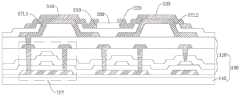
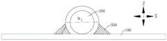
图1是本发明实施例提供的一种显示面板的结构示意图;FIG. 1 is a schematic structural diagram of a display panel provided by an embodiment of the present invention;
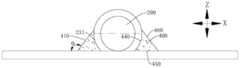
图2是图1中A-A处的局部剖视图;Fig. 2 is a partial cross-sectional view at A-A place in Fig. 1;
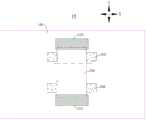
图3是图1中D-D处的局部剖视图;Fig. 3 is a partial sectional view at D-D place among Fig. 1;
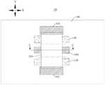
图4是本发明另一实施例提供的一种显示面板的结构示意图;Fig. 4 is a schematic structural diagram of a display panel provided by another embodiment of the present invention;
图5是图4中B-B处的局部剖视图Fig. 5 is a partial cross-sectional view at B-B in Fig. 4
图6是本发明又一实施例提供的一种显示面板的结构示意图;Fig. 6 is a schematic structural diagram of a display panel provided by another embodiment of the present invention;
图7是本发明还一实施例提供的一种显示面板的结构示意图;Fig. 7 is a schematic structural diagram of a display panel provided by another embodiment of the present invention;
图8是图7中C-C处的局部剖视图;Fig. 8 is a partial sectional view at C-C place among Fig. 7;
图9是本发明再一实施例提供的一种显示面板的结构示意图;FIG. 9 is a schematic structural diagram of a display panel provided by yet another embodiment of the present invention;
图10是本发明再一实施例提供的一种显示面板的结构示意图;Fig. 10 is a schematic structural diagram of a display panel provided by yet another embodiment of the present invention;
图11是本发明再一实施例提供的一种显示面板的结构示意图;Fig. 11 is a schematic structural diagram of a display panel provided by yet another embodiment of the present invention;
图12是本发明实施例提供的一种显示面板的制备方法的流程示意图。FIG. 12 is a schematic flowchart of a method for manufacturing a display panel provided by an embodiment of the present invention.
附图标记说明:Explanation of reference signs:
10、显示面板;10. Display panel;
100、基板;100. Substrate;
200、发光元件;210、第一连接端;220、第二连接端;230、侧壁; 231、第一部分侧壁;200, light-emitting element; 210, first connection end; 220, second connection end; 230, side wall; 231, first part side wall;
300、电极元件;310、第一接触电极;320、第二接触电极;300, electrode element; 310, first contact electrode; 320, second contact electrode;
400、辅助绝缘部;410、第一表面;420、第一绝缘部;430、第二绝缘部;440、邻接边;450、第一线性边;460、第二线性边;400, auxiliary insulating portion; 410, first surface; 420, first insulating portion; 430, second insulating portion; 440, adjacent edge; 450, first linear edge; 460, second linear edge;
500、金属覆盖部;500. Metal covering part;
a、外夹角;Q、夹角区域;NA1、第一半导体区域;NA2、第二半导体区域;AA、发光区域;Y、第一方向;X、第二方向;Z、厚度方向。a, outer angle; Q, angle area; NA1, first semiconductor region; NA2, second semiconductor region; AA, light emitting region; Y, first direction; X, second direction; Z, thickness direction.
具体实施方式Detailed ways
下面将详细描述本发明的各个方面的特征和示例性实施例。在下面的详细描述中,提出了许多具体细节,以便提供对本发明的全面理解。但是,对于本领域技术人员来说很明显的是,本发明可以在不需要这些具体细节中的一些细节的情况下实施。下面对实施例的描述仅仅是为了通过示出本发明的示例来提供对本发明的更好的理解。在附图和下面的描述中,至少部分的公知结构和技术没有被示出,以便避免对本发明造成不必要的模糊;并且,为了清晰,可能夸大了部分结构的尺寸。此外,下文中所描述的特征、结构或特性可以以任何合适的方式结合在一个或更多实施例中。Features and exemplary embodiments of various aspects of the invention will be described in detail below. In the following detailed description, numerous specific details are set forth in order to provide a thorough understanding of the present invention. It will be apparent, however, to one skilled in the art that the present invention may be practiced without some of these specific details. The following description of the embodiments is only to provide a better understanding of the present invention by showing examples of the present invention. In the drawings and the following description, at least some well-known structures and techniques have not been shown in order to avoid unnecessarily obscuring the present invention; and, for clarity, the dimensions of some structures may have been exaggerated. Furthermore, the features, structures, or characteristics described hereinafter may be combined in any suitable manner in one or more embodiments.
在本发明的描述中,需要说明的是,除非另有说明,“多个”的含义是两个以上;术语“上”、“下”、“左”、“右”、“内”、“外”等指示的方位或位置关系仅是为了便于描述本发明和简化描述,而不是指示或暗示所指的装置或元件必须具有特定的方位、以特定的方位构造和操作,因此不能理解为对本发明的限制。此外,术语“第一”、“第二”等仅用于描述目的,而不能理解为指示或暗示相对重要性。In the description of the present invention, it should be noted that unless otherwise specified, the meaning of "plurality" is more than two; the terms "upper", "lower", "left", "right", "inner", " The orientation or positional relationship indicated by "outside" and so on are only for the convenience of describing the present invention and simplifying the description, and do not indicate or imply that the referred device or element must have a specific orientation, be constructed and operated in a specific orientation, and therefore cannot be construed as a reference to this invention. Invention Limitations. In addition, the terms "first", "second", etc. are used for descriptive purposes only, and should not be construed as indicating or implying relative importance.
下述描述中出现的方位词均为图中示出的方向,并不是对本发明的实施例的具体结构进行限定。在本发明的描述中,还需要说明的是,除非另有明确的规定和限定,术语“安装”、“连接”应做广义理解,例如,可以是固定连接,也可以是可拆卸连接,或一体地连接;可以是直接相连,也可以间接相连。对于本领域的普通技术人员而言,可视具体情况理解上述术语在本发明中的具体含义。The orientation words appearing in the following description are all directions shown in the figure, and do not limit the specific structure of the embodiment of the present invention. In the description of the present invention, it should also be noted that, unless otherwise specified and limited, the terms "installation" and "connection" should be understood in a broad sense, for example, it can be a fixed connection or a detachable connection, or Connected integrally; either directly or indirectly. For those skilled in the art, the specific meanings of the above terms in the present invention can be understood according to specific situations.
为了更好地理解本发明,下面结合图1至图12对本发明实施例的显示面板、显示装置及显示面板的制备方法进行详细描述。In order to better understand the present invention, the display panel, the display device and the manufacturing method of the display panel according to the embodiment of the present invention will be described in detail below with reference to FIG. 1 to FIG. 12 .
请参阅图1和图2,图1为本发明第一方面实施例提供的一种显示面板的结构示意图。图2是图1中A-A处的局部剖视图。Please refer to FIG. 1 and FIG. 2 . FIG. 1 is a schematic structural diagram of a display panel provided by an embodiment of the first aspect of the present invention. Fig. 2 is a partial sectional view at A-A in Fig. 1 .
如图1和图2所示,显示面板10包括基板100和设置于基板100的发光元件200,发光元件200包括在第一方向(图1中的Y方向)上相对设置的第一连接端210和第二连接端220,发光元件200的侧壁230与基板 100的外表面之间存在夹角区域Q。发光元件200例如为nano-LED器件。在其他实施例中,发光元件200还可以为Micro LED器件、mini LED器件等。As shown in FIGS. 1 and 2 , the
请参阅图3,图3是图1中D-D处的剖视图。图3和图2的不同之处在于更具体的展示了基板100的部分层结构。Please refer to FIG. 3 . FIG. 3 is a cross-sectional view at D-D in FIG. 1 . The difference between FIG. 3 and FIG. 2 is that the partial layer structure of the
可选的,基板100包括衬底110和设置于衬底的驱动器件层120,驱动器件层120例如包括薄膜晶体管(Thin Film Transistor,TFT)器件,以通过TFT器件驱动发光元件200发光。Optionally, the
可选的,显示面板10还包括第一电极ETL1、第二电极ETL2、第一接触电极310和第二接触电极320,第一电极ETL1、第二电极ETL2与第一接触电极310、第二接触电极320之间设置有绝缘层。第一接触电极 310和第一连接端210相互连接,第二接触电极320与第二连接端220相互连接。第一接触电极310可以设置在第一电极ETL1上,以与第一电极 ETL1接触。第一接触电极310可以在第一电极ETL1的未被绝缘层覆盖的一个区域上与第一电极ETL1接触。第一接触电极310可以位于至少一个发光元件200的一个端部上。例如,与第一电极ETL1相邻的多个发光元件200可以在相应的发光元件200的一个端部处与第一电极ETL1接触。即,第一接触电极310可以覆盖发光元件200的第一连接端210和第一电极ETL1的与其对应的至少一个区域。因此,发光元件200的第一连接端 210可以通过第一接触电极310电连接到第一电极ETL1。同理,发光元件 200的第二连接端220可以通过第二接触电极320电连接到第二电极 ETL2。Optionally, the
发光元件200通常为立体结构件,例如发光元件200为棱柱状或圆柱状,立体结构的发光元件200和基板100之间会形成段差。在将nano-LED 器件转移至基板100之后,至少还需要制备第一接触电极310和第二接触电极320等金属层以驱动发光元件200发光。由于立体结构的发光元件 200和基板100之间会形成段差,后续制成中容易出现金属残留导致nano- LED器件被短路而影响nano-LED显示器的良率。如图2所示,本发明实施例体发光元件200为圆柱状进行举例说明,在其他实施例中,发光元件 200还可以呈棱柱状或其他立体形状。The
当发光元件200呈圆柱状时,发光元件200具有与基板100所在平面平行、且经过中心轴线的最大横截面(即图2中直线M所在的截面)。发光元件200设置于基板100时,发光元件200的中心轴线和基板100所在平面平行设置。这就导致发光元件200的侧壁230和基板100表面之间会形成上述的夹角区域Q,且发光元件200的最大横截面会遮挡部分夹角区域Q。在后续制备第一接触电极310和第二接触电极320的光刻胶工艺中,夹角区域Q内容易形成光刻胶残留,进而导致刻蚀残留,形成金属残留,导致第一接触电极310和第二接触电极320相互连接形成短路影响显示面板10的良率。When the light-emitting
可选的,当发光元件200为圆柱形时,侧壁230在第二方向(图1中的X方向)上的两端均与基板100表面之间形成夹角区域Q,第二方向X 与第一方向Y相交。如图2所示,夹角区域Q由基板100上不与发光元件 200接触的表面与发光元件200的侧壁230相交形成。Optionally, when the light-emitting
请一并参阅图1至图5,图4为本发明第一方面另一实施例提供的一种显示面板10的结构示意图。图5是图4中B-B处的局部剖视图。Please refer to FIG. 1 to FIG. 5 together. FIG. 4 is a schematic structural diagram of a
如图4和图5所示,显示面板10还包括:电极元件300,设置于基板 100,电极元件300包括上述的第一接触电极310和第二接触电极320,第一接触电极310连接于第一连接端210,第二接触电极320连接于第二连接端220;辅助绝缘部400,至少部分辅助绝缘部400位于第一接触电极 310和第二接触电极320之间并设置于夹角区域Q。即至少部分辅助绝缘部400位于第一接触电极310在第一方向Y上朝向第二接触电极320的一侧。As shown in Figure 4 and Figure 5, the
在本发明实施例提供的显示面板10中,显示面板10包括基板100、设置于基板100的发光元件200、电极元件300和辅助绝缘部400。电极元件300包括第一接触电极310和第二接触电极320,第一接触电极310 和第二接触电极320分别连接于发光元件200的第一连接端210和第二连接端220,使得电极元件300能够驱动发光元件200发光,实现显示面板 10的显示。In the
如上所述,发光元件200和基板100表面之间会形成夹角区域Q,该夹角区域Q极易形成金属残留。辅助绝缘部400位于夹角区域Q,即辅助绝缘部400能够填充至少部分夹角区域Q,辅助绝缘部400占据部分夹角区域Q的空间,因而能够改善制备第一接触电极310和第二接触电极320 时在夹角区域Q形成的金属残留。辅助绝缘部400位于第一接触电极310 和第二接触电极320之间,能够改善第一接触电极310和第二接触电极 320之间的金属残留,改善由于金属残留导致的第一接触电极310和第二接触电极320相互连接形成的短路,能够有效提高显示面板10的良率。As mentioned above, an angle region Q is formed between the light emitting
可选的,当对应于同一发光元件200具有两个夹角区域Q时,各夹角区域Q内均设置有至少部分辅助绝缘部400。Optionally, when there are two included angle regions Q corresponding to the same
辅助绝缘部400的制备方式有多种,可选的,可以在设置发光元件 200以后继续制备形成绝缘层,对绝缘层进行图案化处理形成辅助绝缘部 400。并在形成辅助绝缘部400后制备第一接触电极310和第二接触电极 320,使得辅助绝缘部400能够先于金属残留占据夹角区域Q,更好的改善夹角区域Q形成的金属残留。There are many ways to prepare the auxiliary insulating
辅助绝缘部400的尺寸设置方式有多种,在一些可选的实施例中,请继续参阅图4和图5,沿第一方向Y,辅助绝缘部400的尺寸大于发光元件200的尺寸,且第一连接端210和第二连接端220由辅助绝缘部400露出,至少部分电极元件300位于辅助绝缘部400背离基板100的一侧。There are many ways to set the size of the auxiliary insulating
在这些可选的实施例中,辅助绝缘部400的尺寸较大,辅助绝缘部 400能够延伸至第一连接端210背离第二连接端220的一侧,且辅助绝缘部400也能够延伸至第二连接端220背离第一连接端210的一侧。使得夹角区域Q在第一方向Y上的不同部位均能够被辅助绝缘部400填充,更好地改善金属残留问题。In these optional embodiments, the size of the auxiliary insulating
为了令第一连接端210和第二连接端220由辅助绝缘部400露出,在一些可选的实施例中,沿显示面板10的厚度方向(图5中的Z方向),辅助绝缘部400的最大延伸厚度小于发光元件200的最大延伸厚度。在这些可选的实施例中,当在发光元件200上沉积形成辅助绝缘部400时,由于辅助绝缘部400的厚度较小,使得辅助绝缘部400不会完全覆盖第一连接端210和第二连接端220。之后沉积形成第一接触电极310和第二接触电极320时,第一接触电极310可以直接与第一连接端210相互接触连接,第二接触电极320也能够与第二连接端220相互接触连接。In order to expose the first connecting
在其他实施例中,辅助绝缘部400的最大延伸厚度也可以大于或等于发光元件200的最大厚度。在沉积形成辅助绝缘部400以后,对辅助绝缘部400进行图案化处理形成过孔,使得第一连接端210和第二连接端220 可以由过孔露出。之后沉积形成第一接触电极310和第二接触电极320 时,第一接触电极310可以通过过孔与第一连接端210相互接触连接,第二接触电极320也可以通过过孔与第二连接端220相互接触连接。In other embodiments, the maximum extended thickness of the auxiliary insulating
在一些可选的实施例中,如图4和图5所示,辅助绝缘部400具有连接在侧壁230和基板100表面之间且不与基板100表面和侧壁230面接触的第一表面410,侧壁230具有连接于外表面和基板100表面之间的且与辅助绝缘部400接触的第一部分侧壁231,第一表面410和基板100表面之间的外夹角a大于第一部分侧壁231与基板100表面之间的夹角。In some optional embodiments, as shown in FIG. 4 and FIG. 5 , the auxiliary insulating
需要说明的是,第一表面410和基板100表面之间的外夹角a是指:在发光元件200在第二方向X上的同侧,基板100表面包括不被辅助绝缘部400覆盖的第三表面,第三表面与第一表面410的部分边界相交,第三表面与第一表面410之间的夹角为第一表面410和基板100表面之间的外夹角a。侧壁230通过第一部分侧壁231与辅助绝缘部400面面接触。It should be noted that the outer angle a between the
在这些可选的实施例中,第一表面410和基板100表面之间的外夹角 a大于第一部分侧壁231与基板100表面之间的夹角,即外夹角a的取值较大。第一表面410与基板100表面之间形成的斜坡相比于第一部分侧壁 231与基板100表面形成的斜坡的坡度更缓,第一表面410和基板100表面的夹角处更不易形成金属残留。因此能够更好的改善第一接触电极310 和第二接触电极320之间的金属残留,改善由于金属残留导致的第一接触电极310和第二接触电极320相互连接形成的短路,能够有效提高显示面板10的良率。In these optional embodiments, the outer angle a between the
可选的,辅助绝缘部400的最大厚度大于或等于发光元件200的最大横截面至基板100表面的距离。当辅助绝缘部400的最大厚度大于或等于最大横截面至基板100表面的距离时,保证辅助绝缘部400能够填充最大横截面和基板100表面之间的间隙,不会形成内间隙,能够更好的改善金属残留。Optionally, the maximum thickness of the auxiliary insulating
例如,第一表面410具有不与发光元件200接触的自由端,且第一表面410通过该自由端与基板100表面接触。发光元件200在基板100的正投影不与该自由端交叠,即该自由端不被发光元件200覆盖。在基板100 至发光元件200的方向上,第一表面410由基板100表面沿靠近发光元件 200的方向倾斜,即第一表面410由自由端沿靠近发光元件的方向倾斜,使得第一表面410和基板100表面之间形成的夹角不会被最大横截面覆盖。即第一表面410和基板100表面之间形成的夹角位于发光元件200在第二方向X上的一侧,不易形成刻蚀残留。For example, the
请参阅图6,图6是本发明第一方面又一实施例提供的一种显示面板 10的结构示意图。Please refer to FIG. 6. FIG. 6 is a schematic structural diagram of a
在又一些可选的实施例中,如图6所示,沿第一方向Y,辅助绝缘部 400的尺寸小于或等于发光元件200的尺寸,且辅助绝缘部400位于第一接触电极310和第二接触电极320之间。In still some optional embodiments, as shown in FIG. 6, along the first direction Y, the size of the auxiliary insulating
在这些可选的实施例中,辅助绝缘部400的尺寸较小,且辅助绝缘部 400位于第一接触电极310和第二接触电极320之间,令辅助绝缘部400 与第一接触电极310和/或第二接触电极320间隔设置,即辅助绝缘部400 与第一接触电极310和/或第二接触电极320之间形成位于夹角区域Q的间隙。该间隙对应的夹角区域Q内可能形成金属残留,但是由于辅助绝缘部 400与基板100表面之间存在段差,使得辅助绝缘部400能够截断辅助绝缘部400与第一接触电极310和/或第二接触电极320之间的间隙内的金属残留。因此不易在第一接触电极310和第二接触电极320之间形成连续的金属残留,能够改善由于金属残留导致的第一接触电极310和第二接触电极320相互连接形成的短路,有效提高显示面板10的良率。In these optional embodiments, the size of the auxiliary insulating
可选的,请继续参阅图5,沿厚度方向Z,电极元件300的最大延伸厚度小于辅助绝缘部400的最大延伸厚度。即第一接触电极310和第二接触电极320的最大延伸厚度小于辅助绝缘部400的最大延伸厚度。Optionally, please continue to refer to FIG. 5 , along the thickness direction Z, the maximum extended thickness of the
在这些可选的实施例中,当第一接触电极310和辅助绝缘部400之间具有金属残留时,由于辅助绝缘部400的厚度较大,能够保证该金属残留的厚度小于辅助绝缘部400的厚度。位于辅助绝缘部400两侧的金属残留不会经由辅助绝缘部400的第一表面410相互连通,能够进一步改善由于金属残留导致的第一接触电极310和第二接触电极320相互连接形成的短路,有效提高显示面板10的良率。In these optional embodiments, when there is metal residue between the
请继续参阅图1,发光元件200包括在第一方向Y上分布的第一半导体区域NA1、第二半导体区域NA2及位于第一半导体区域NA1和第二半导体区域NA2之间的发光区域AA。第一半导体区域NA1和第二半导体区域NA2用于设置半导体材料,发光区域AA用于发光。第一半导体区域 NA1通过第一连接端210和第一接触电极310连接,第二半导体区域NA2 通过第二连接端220和第二接触电极320连接。Please continue to refer to FIG. 1 , the
第一连接端210例如可以设置金属层,以使第一半导体区域NA1内的半导体材料通过金属层与第一接触电极310相互连接。或者半导体材料由第一半导体区域NA1延伸至第一连接端210,半导体材料直接与第一接触电极310连接。同样的,第二连接端220例如可以设置金属层,以使第二半导体区域NA2内的半导体材料通过金属层与第二接触电极320相互连接。或者半导体材料由第二半导体区域NA2延伸至第二连接端220,半导体材料直接与第一接触电极310连接。For example, a metal layer may be provided on the
当辅助绝缘部400的尺寸小于发光元件200的尺寸时,辅助绝缘部 400的设置位置有多种。例如,如图6所示,辅助绝缘部400和发光区域 AA错位设置。使得辅助绝缘部400不会遮挡发光区域AA,因此即使设置辅助绝缘部400也不会影响显示面板10的发光效果。When the size of the auxiliary insulating
请参阅图7和图8,图7是本发明第一方面还一实施例提供的一种显示面板10的结构示意图。图8是图7中C-C处的局部剖视图。Please refer to FIG. 7 and FIG. 8 . FIG. 7 is a schematic structural diagram of a
在一些可选的实施例中,显示面板10还包括:金属覆盖部500,至少部分金属覆盖部500位于发光区域AA内的夹角区域Q内。即至少部分金属覆盖部500位于发光区域AA内侧壁230和基板100表面形成的夹角区域Q内,金属覆盖部500对应位于发光区域AA。金属覆盖部500包括金属材料,金属材料能够反射发光区域AA的光线,因而能够提高出光量,提高显示面板10的出光率。In some optional embodiments, the
可选的,请继续参阅图8,沿显示面板10的厚度方向Z,金属覆盖部 500的最大延伸尺寸小于或等于发光元件200最大延伸尺寸的一半。例如当发光元件200呈圆柱形时,金属覆盖部500位于发光元件200的最大横截面之下,能够避免金属覆盖部500覆盖发光区域AA,影响显示面板10 的出光效率。Optionally, please continue to refer to FIG. 8 , along the thickness direction Z of the
当显示面板10既包括金属覆盖部500,也包括辅助绝缘部400时,金属覆盖部500和辅助绝缘部400的相对位置设置方式有多种。When the
在一些可选的实施例中,请继续参阅图7,辅助绝缘部400包括第一绝缘部420和第二绝缘部430,第一绝缘部420对应于第一半导体区域 NA1设置,第二绝缘部430对应于第二半导体区域NA2设置;金属覆盖部500位于第一绝缘部420和第二绝缘部430之间。In some optional embodiments, please continue to refer to FIG. 7, the auxiliary insulating
在这些可选的实施例中,金属覆盖部500在第一方向Y的两侧分别设置有第一绝缘部420和第二绝缘部430。第一绝缘部420能够截断第一接触电极310和金属覆盖部500之间的金属残留,第二绝缘部430能够截断第二接触电极320和金属覆盖部500之间的金属残留,进而改善第一接触电极310和第二接触电极320之间的金属残留,能够改善由于金属残留导致的第一接触电极310和第二接触电极320相互连接形成的短路,有效提高显示面板10的良率。In these optional embodiments, the
请参阅图9,图9是本发明第一方面再一实施例提供的一种显示面板 10的结构示意图。Please refer to FIG. 9. FIG. 9 is a schematic structural diagram of a
在另一些可选的实施例中,辅助绝缘部400和金属覆盖部500一一对应设置,即对应于同一发光元件200,辅助绝缘部400和金属覆盖部500 的个数均为一个。辅助绝缘部400位于金属覆盖部500在第一方向Y上的一侧。例如辅助绝缘部400可以设置于金属覆盖部500和第一接触电极 310之间,或者辅助绝缘部400可以设置于金属覆盖部500和第二接触电极320之间。辅助绝缘部400的设置个数较少,能够改善由于设置辅助绝缘部400对显示面板10出光的影响。In some other optional embodiments, the auxiliary insulating
可选的,如图9所示,当辅助绝缘部400设置于金属覆盖部500和第一接触电极310之间时,金属覆盖部500和第二接触电极320同层同材料设置,且金属覆盖部500和第二接触电极320相互连接。使得金属覆盖部 500和电极元件300能够在同一工艺步骤中制备成型,且能够降低对金属层的刻蚀要求。使得金属覆盖部500可以由制备第二接触电极320时形成的金属残留形成,能够简化显示面板10的制备工艺,提高显示面板10的制备效率。Optionally, as shown in FIG. 9, when the auxiliary insulating
可选的,请参阅图10和图11,图10是本发明第一方面再一实施例提供的一种显示面板10的结构示意图,图11是与图10不同的本发明第一方面再一实施例提供的一种显示面板10的结构示意图。如图10和图11所示,当辅助绝缘部400设置于金属覆盖部500和第二接触电极320之间时,金属覆盖部500和第一接触电极310同层同材料设置,且金属覆盖部 500和第一接触电极310相互连接。使得金属覆盖部500和电极元件300 能够在同一工艺步骤中制备成型,且能够降低对金属层的刻蚀要求。使得金属覆盖部500可以由制备第一接触电极310时形成的金属残留形成,能够简化显示面板10的制备工艺,提高显示面板10的制备效率。Optionally, please refer to Fig. 10 and Fig. 11. Fig. 10 is a schematic structural diagram of a
在一些可选的实施例中,沿显示面板10的厚度方向Z,辅助绝缘部 400的最大延伸厚度小于发光元件200的最大延伸厚度。通常,第一表面 410与发光元件200的侧壁230接触的一端与基板100表面之间的间距最大,第一表面410与发光元件200侧壁230接触的一端与基板100表面之间的间距为辅助绝缘部400的最大延伸厚度。In some optional embodiments, along the thickness direction Z of the
在这些可选的实施例中,当辅助绝缘部400的最大延伸厚度小于发光元件200的最大延伸厚度,能够避免在辅助绝缘部400的制备过程中绝缘材料完全覆盖第一连接端210和第二连接端220,影响后续第一连接端 210和第一接触电极310的连接良率、及第二连接端220和第二接触电极 320之间的连接良率。In these optional embodiments, when the maximum extended thickness of the auxiliary insulating
可选的,辅助绝缘部400的最大延伸厚度大于或等于1μm。能够改善由于辅助绝缘部400厚度不足导致金属残留能够连接第一接触电极310 和第二接触电极320形成短路。Optionally, the maximum extended thickness of the auxiliary insulating
在一些可选的实施例中,请继续参阅图5,位于第一接触电极310和第二接触电极320之间的辅助绝缘部400沿垂直于第一方向Y的截面呈类三角形,类三角形包括邻接边440、第一线性边450和第二线性边460,邻接边440与发光元件200侧壁230相邻,第一线性边450与基板100相邻,第一线性边450与第二线性边460之间的夹角小于或等于70°。第二线性边460是由第一表面410的横截面形成的边。In some optional embodiments, please continue to refer to FIG. 5 , the auxiliary insulating
当第一线性边450与第二线性边460之间的夹角小于或等于70°时,外夹角a大于或等于180°-70°,即外夹角a大于或等于110°,能够保证第一表面410相对基板100表面形成的坡度较缓,改善第一表面410和基板100表面夹角处的金属残留。When the angle between the first
本发明第二方面的实施例还提供一种显示装置,包括上述任一第一方面实施例的显示面板10。由于本发明第二方面实施例提供的显示装置包括上述第一方面任一实施例的显示面板10,因此本发明第二方面实施例提供的显示装置具有上述第一方面任一实施例的显示面板10具有的有益效果,在此不再赘述。The embodiment of the second aspect of the present invention further provides a display device, including the
本发明实施例中的显示装置包括但不限于手机、个人数字助理 (PersonalDigital Assistant,简称:PDA)、平板电脑、电子书、电视机、门禁、智能固定电话、控制台等具有显示功能的设备。The display devices in the embodiments of the present invention include but are not limited to mobile phones, personal digital assistants (Personal Digital Assistant, PDA for short), tablet computers, e-books, televisions, access control, smart fixed phones, consoles and other devices with display functions.
请参阅图12,图12是本发明第三方面实施例提供的一种显示面板10 的制备方法的流程示意图。Please refer to FIG. 12. FIG. 12 is a schematic flow chart of a method for manufacturing a
如图12所示,本发明第三方面的实施还提供一种显示面板10的制备方法,显示面板10可以为上述任一第一方面实施例的显示面板10。制备方法包括:As shown in FIG. 12 , the implementation of the third aspect of the present invention also provides a method for manufacturing a
步骤S01:提供一种基板100。Step S01 : providing a
步骤S02:在基板100上布设发光元件200,发光元件200包括在第一方向Y上相对设置的第一连接端210和第二连接端220,发光元件200 的侧壁230与基板100表面之间存在夹角区域Q。Step S02: Arranging the light-emitting
步骤S03:在发光元件200上制备绝缘层,对绝缘层进行图案化处理形成辅助绝缘部400,至少部分辅助绝缘部400位于第一连接端210和第二连接端220之间并设置于夹角区域Q。Step S03: Prepare an insulating layer on the light-emitting
步骤S04:沉积金属层并对金属层图案化处理形成第一接触电极310 和第二接触电极320,第一接触电极310连接于第一连接端210,第二接触电极320连接于第二连接端220。Step S04: Depositing a metal layer and patterning the metal layer to form a
在本发明实施例提供的显示面板10的制备方法中,首先通过步骤S02 将发光元件200布设于基板100上。由于发光元件200为立体结构件,发光元件200的侧壁230与基板100表面之间会形成夹角区域Q,该夹角区域Q极易形成金属残留。然后通过步骤S03在发光元件200上制备辅助绝缘部400,辅助绝缘部400先于金属残留位于夹角区域Q内,辅助绝缘部400位于第一连接端210和第二连接端220之间,能够改善第一连接端210 和第二连接端220的金属残留。最后通过步骤S04沉积金属层,此时由于夹角区域Q内已经存在辅助绝缘部400,因此能够改善夹角区域Q内的金属残留,改善由于金属残留导致的第一接触电极310和第二接触电极320 相互连接形成的短路,能够有效提高显示面板10的良率。In the manufacturing method of the
可选的,如上所述,当沿第一方向Y,辅助绝缘部400的尺寸大于发光元件200的尺寸,且辅助绝缘部400的最大延伸厚度大于发光元件200 的最大厚度时,在步骤S03中对绝缘层进行图案化处理时,还在辅助绝缘部400上形成两个过孔,使得第一连接端210和第二连接端220均能够由过孔露出。以保证在步骤S04中沉积金属层时,金属材料可以经由过孔与第一连接端210和第二连接端220接触连接。Optionally, as described above, when along the first direction Y, the size of the auxiliary insulating
可选的,如上所述,当辅助绝缘部400和发光区域AA错位设置时,在步骤S03中,辅助绝缘部400对应位于第一半导体区域NA1和/或第二半导体区域NA2,即辅助绝缘部400和发光区域AA错位设置。Optionally, as described above, when the auxiliary insulating
在一些可选的实施例中,在步骤S04中对金属层进行图案化处理时,对金属层进行图案化处理还形成金属覆盖部500,至少部分金属覆盖部 500位于发光区域AA内的夹角区域Q内。金属覆盖部500的有益效果如上所述,不再赘述。金属覆盖部500和第一接触电极310、第二接触电极 320在同一工艺步骤S04中形成,在提高显示面板10出光效果的同时,还能够简化显示面板10的制备方法,提高显示面板10的制备效率。In some optional embodiments, when the metal layer is patterned in step S04, the metal layer is patterned to form a
在一些可选的实施例中,在步骤S03中形成的辅助绝缘部400位于第一半导体区域NA1,第一半导体区域NA1和第一接触电极310相邻。那么在步骤S04中:对金属层进行图案化处理还形成金属覆盖部500,金属覆盖部500由第二接触电极320延伸至发光区域AA。即金属覆盖部500 由制备第二接触电极320的金属残留形成,能够进一步简化显示面板10 的制备方法。In some optional embodiments, the auxiliary insulating
在另一些可选的实施例中,在步骤S03中形成的辅助绝缘部400位于第二半导体区域NA2,第二半导体区域NA2和第二接触电极320相邻。那么在步骤S04中:对金属层进行图案化处理还形成金属覆盖部500,金属覆盖部500由第一接触电极310延伸至发光区域AA。即金属覆盖部500 由制备第一接触电极310的金属残留形成,能够进一步简化显示面板10 的制备方法。In other optional embodiments, the auxiliary insulating
虽然已经参考优选实施例对本申请进行了描述,但在不脱离本申请的范围的情况下,可以对其进行各种改进并且可以用等效物替换其中的部件。尤其是,只要不存在结构冲突,各个实施例中所提到的各项技术特征均可以任意方式组合起来。本申请并不局限于文中公开的特定实施例,而是包括落入权利要求的范围内的所有技术方案。While the application has been described with reference to a preferred embodiment, various modifications may be made and equivalents may be substituted for elements thereof without departing from the scope of the application. In particular, as long as there is no structural conflict, the technical features mentioned in the various embodiments can be combined in any manner. The present application is not limited to the specific embodiments disclosed herein, but includes all technical solutions falling within the scope of the claims.
Claims (19)
Priority Applications (1)
| Application Number | Priority Date | Filing Date | Title |
|---|---|---|---|
| CN202110743725.XACN113571619B (en) | 2021-06-30 | 2021-06-30 | Display panel, display device and preparation method of display panel |
Applications Claiming Priority (1)
| Application Number | Priority Date | Filing Date | Title |
|---|---|---|---|
| CN202110743725.XACN113571619B (en) | 2021-06-30 | 2021-06-30 | Display panel, display device and preparation method of display panel |
Publications (2)
| Publication Number | Publication Date |
|---|---|
| CN113571619A CN113571619A (en) | 2021-10-29 |
| CN113571619Btrue CN113571619B (en) | 2023-04-07 |
Family
ID=78163375
Family Applications (1)
| Application Number | Title | Priority Date | Filing Date |
|---|---|---|---|
| CN202110743725.XAActiveCN113571619B (en) | 2021-06-30 | 2021-06-30 | Display panel, display device and preparation method of display panel |
Country Status (1)
| Country | Link |
|---|---|
| CN (1) | CN113571619B (en) |
Citations (4)
| Publication number | Priority date | Publication date | Assignee | Title |
|---|---|---|---|---|
| JP2012094885A (en)* | 2011-12-09 | 2012-05-17 | Sharp Corp | Light emitting device, back light, lighting apparatus, and display device |
| KR101768956B1 (en)* | 2016-07-29 | 2017-08-18 | 엘지디스플레이 주식회사 | Organic Light Emitting Diode Device AND Method for Manufacturing thereof |
| CN108206228A (en)* | 2016-12-19 | 2018-06-26 | 三星显示有限公司 | Light emitting device and method of manufacturing light emitting device |
| KR20200063411A (en)* | 2018-11-27 | 2020-06-05 | 삼성디스플레이 주식회사 | Light emitting element, method of manufacturing the same and the display device comprising the light emitting element |
Family Cites Families (3)
| Publication number | Priority date | Publication date | Assignee | Title |
|---|---|---|---|---|
| KR102608419B1 (en)* | 2016-07-12 | 2023-12-01 | 삼성디스플레이 주식회사 | Display Apparatus and Method for manufacturing the same |
| KR102606922B1 (en)* | 2018-07-06 | 2023-11-27 | 삼성디스플레이 주식회사 | Display device and Method of manufacturing the same |
| KR102559097B1 (en)* | 2018-07-27 | 2023-07-26 | 삼성디스플레이 주식회사 | Light emitting device, fabricating method thereof, and display device including the same |
- 2021
- 2021-06-30CNCN202110743725.XApatent/CN113571619B/enactiveActive
Patent Citations (4)
| Publication number | Priority date | Publication date | Assignee | Title |
|---|---|---|---|---|
| JP2012094885A (en)* | 2011-12-09 | 2012-05-17 | Sharp Corp | Light emitting device, back light, lighting apparatus, and display device |
| KR101768956B1 (en)* | 2016-07-29 | 2017-08-18 | 엘지디스플레이 주식회사 | Organic Light Emitting Diode Device AND Method for Manufacturing thereof |
| CN108206228A (en)* | 2016-12-19 | 2018-06-26 | 三星显示有限公司 | Light emitting device and method of manufacturing light emitting device |
| KR20200063411A (en)* | 2018-11-27 | 2020-06-05 | 삼성디스플레이 주식회사 | Light emitting element, method of manufacturing the same and the display device comprising the light emitting element |
Also Published As
| Publication number | Publication date |
|---|---|
| CN113571619A (en) | 2021-10-29 |
Similar Documents
| Publication | Publication Date | Title |
|---|---|---|
| CN114144886B (en) | Display substrate, manufacturing method thereof, and display device | |
| CN112117321B (en) | Display panel and manufacturing method thereof | |
| CN110544714A (en) | Display panel, manufacturing method thereof, and display device | |
| CN111090203B (en) | Array substrate and display panel | |
| CN111463243A (en) | Array substrate and preparation method thereof | |
| CN108461525A (en) | Display master blank, display base plate and display device | |
| CN109065590B (en) | Organic light-emitting display substrate and method of making the same, and organic light-emitting display device | |
| CN115440913B (en) | Display panel and display device | |
| CN111276492B (en) | Display device, OLED panel, and method for manufacturing OLED panel | |
| CN111725279B (en) | Array substrate and OLED display panel | |
| TW202147281A (en) | Display apparatus | |
| CN117460305A (en) | Display panel and display device | |
| CN114902422B (en) | Display panel, manufacturing method and display device thereof | |
| CN110265460A (en) | Oled display substrate and preparation method thereof, display device | |
| CN113571619B (en) | Display panel, display device and preparation method of display panel | |
| CN117242918A (en) | Display panel, manufacturing method thereof and display device | |
| US11532264B2 (en) | Driving backplane and method for manufacturing the same, and display panel | |
| CN111081723B (en) | Array substrate, manufacturing method of array substrate, display panel and display device | |
| CN110211968A (en) | A kind of display base plate and preparation method thereof, display device | |
| CN218998737U (en) | Display substrate, display panel and display device | |
| CN111725281A (en) | Display modules and electronic equipment | |
| CN117412640A (en) | Display panel, display device and preparation method of display panel | |
| CN114927627A (en) | Display panel, manufacturing method thereof and display device | |
| CN117178654A (en) | OLED display panel | |
| CN207868203U (en) | Display master blank, display base plate and display device |
Legal Events
| Date | Code | Title | Description |
|---|---|---|---|
| PB01 | Publication | ||
| PB01 | Publication | ||
| SE01 | Entry into force of request for substantive examination | ||
| SE01 | Entry into force of request for substantive examination | ||
| GR01 | Patent grant | ||
| GR01 | Patent grant |