CN1134849C - led - Google Patents
ledDownload PDFInfo
- Publication number
- CN1134849C CN1134849CCNB991191536ACN99119153ACN1134849CCN 1134849 CCN1134849 CCN 1134849CCN B991191536 ACNB991191536 ACN B991191536ACN 99119153 ACN99119153 ACN 99119153ACN 1134849 CCN1134849 CCN 1134849C
- Authority
- CN
- China
- Prior art keywords
- semiconductor
- type surface
- electrode
- layer
- gallium nitride
- Prior art date
- Legal status (The legal status is an assumption and is not a legal conclusion. Google has not performed a legal analysis and makes no representation as to the accuracy of the status listed.)
- Expired - Lifetime
Links
Images


Landscapes
- Led Devices (AREA)
Abstract
Description
Translated fromChinese技术领域technical field
本发明涉及一种发光二极管,尤其是一种具有较小芯片面积的发光二极管。The invention relates to a light emitting diode, especially a light emitting diode with a smaller chip area.
背景技术Background technique
发光二极管的应用颇为广泛,例如,可应用于光学显示装置、交通标志、交通信号标志、数据储存装置、通信装置、照明装置以及医疗装置。在此技术领域中,目前技术人员的重要课题之一是如何减小发光二极管芯片的尺寸,使得自预定尺寸的晶片,能够切害出较多的芯片,因而能够达到降低发光二极管芯片的成本。此外,二极管芯片的尺寸愈小,将数个此种二极管使用于一阵列装置中时,更能够提供较高的解析度。Light-emitting diodes are widely used, for example, in optical display devices, traffic signs, traffic signal signs, data storage devices, communication devices, lighting devices, and medical devices. In this technical field, one of the important issues for technicians at present is how to reduce the size of LED chips so that more chips can be cut out from a wafer with a predetermined size, thereby reducing the cost of LED chips. In addition, the smaller the size of the diode chips, the better resolution can be provided when several of these diodes are used in an array device.
目前市面上,制造发光二极管一般是以蓝宝石作绝缘衬底,在其上形成氮化镓系III-V族化合物半导体,构成发光二极管,例如,由Nakamura等人申请的美国专利第5,652,434号中所公开的一种氮化镓系III-V族化合物半导体,其中的P型电极与N型电极,皆配置于其正方形发光表面的对角线上,其芯片尺寸仍存在可减小的空间。Currently on the market, sapphire is generally used as an insulating substrate in the manufacture of light-emitting diodes, on which gallium nitride-based III-V compound semiconductors are formed to form light-emitting diodes. In the disclosed gallium nitride-based III-V group compound semiconductor, the P-type electrodes and N-type electrodes are arranged on the diagonals of the square light-emitting surface, and there is still room for reducing the chip size.
发明内容Contents of the invention
本发明的主要目的在于提供一种可提供较高解析度的发光二极管,并能够提供较小的芯片尺寸,因而能够降低发光二极首芯片的成本。The main purpose of the present invention is to provide a light-emitting diode with higher resolution and smaller chip size, thereby reducing the cost of the first chip of the light-emitting diode.
根据本发明,提供一种发光二极管,包括:一长方形绝缘衬底,一氮化镓半导体叠层、AlxGa1-xN半导体束缚层,其中0≤x≤1、一氮化镓多重量子阱发光层、一第一电极及一第二电极,其中:According to the present invention, a light-emitting diode is provided, comprising: a rectangular insulating substrate, a gallium nitride semiconductor stack, anAlxGa1-xN semiconductor confinement layer, wherein 0≤x≤1, a gallium nitride multiquantum Well light-emitting layer, a first electrode and a second electrode, wherein:
长方形绝缘衬底,具有一第一主表面与一第二主表面;a rectangular insulating substrate having a first main surface and a second main surface;
半导体叠层,具有一第一主表面、一第二主表面及一第三主表面,半导体叠层经第二主表面与该绝缘衬底的第一主表面结合,其第一主表面与第三主表面位于绝缘衬底的第一主表面的同一侧,其第一主表面与第二主表面分别位于半导体叠层的第三主表面的二相对侧;半导体叠层包括:The semiconductor stack has a first main surface, a second main surface and a third main surface, the semiconductor stack is combined with the first main surface of the insulating substrate through the second main surface, the first main surface and the second main surface The three main surfaces are located on the same side of the first main surface of the insulating substrate, and the first main surface and the second main surface are respectively located on two opposite sides of the third main surface of the semiconductor stack; the semiconductor stack includes:
发光层,具有一第一主表面与一第二主表面:The light-emitting layer has a first main surface and a second main surface:
一第一半导体束缚层,具有第一导电性,且具有一第一主表面与一第二主表面,第一半导体束缚层的第二主表面与发光层的第一主表面结合;及A first semiconductor constraining layer having a first conductivity and having a first main surface and a second main surface, the second main surface of the first semiconductor constraining layer is combined with the first main surface of the light-emitting layer; and
一第二半导体束缚层,具有第二导电性,具有一第一主表面与一第二主表面,第二半导体束缚层的第一主表面与发光层的第二主表面结合;A second semiconductor constraining layer having a second conductivity and having a first main surface and a second main surface, the first main surface of the second semiconductor constraining layer is combined with the second main surface of the light-emitting layer;
第一电极,具有第一导电性,且与半导体叠层的第一主表面结合,第一电极与第一半导体束缚层电连通;以及a first electrode having a first conductivity and bonded to the first major surface of the semiconductor stack, the first electrode being in electrical communication with the first semiconductor bound layer; and
第二电极,具有第二导电性,且在一预定位置与半导体叠层的第三主表面结合,第二电极与第二半导体束缚层电连通;The second electrode has a second conductivity and is combined with the third main surface of the semiconductor stack at a predetermined position, and the second electrode is in electrical communication with the second semiconductor binding layer;
其中有自该第一电极至该第二电极的多个电流路径依序通过和第一半导体束缚层、发光层及第二半导体束缚层;其中,第一电极与第二电极并排在长方形的纵方向。There are a plurality of current paths from the first electrode to the second electrode passing through the first semiconductor confinement layer, the light-emitting layer and the second semiconductor confinement layer in sequence; wherein, the first electrode and the second electrode are arranged side by side in the longitudinal direction of a rectangle direction.
优选地,所述半导体叠层更包括:Preferably, the semiconductor stack further includes:
一第一半导体接触层,具有第一导电性,且具有一第一主表面与一第二主表面,此第一半导体接触层的第二主表面与第一半导体束缚层的第一主表面结合;及A first semiconductor contact layer having first conductivity and having a first main surface and a second main surface, the second main surface of the first semiconductor contact layer is combined with the first main surface of the first semiconductor confinement layer ;and
一第二半导体接触层,具有第二导电性,且具有一第一主表面与一第二主表面,第二半导体接触层的第一主表面与第二半导体束缚层的第二主表面结合;A second semiconductor contact layer having a second conductivity and having a first main surface and a second main surface, the first main surface of the second semiconductor contact layer is combined with the second main surface of the second semiconductor binding layer;
其中有自所述第一电极至第二电极的数电流路径依序通过所述第一半导体接触层、所述第一半导体束缚层、发光层、第二半导体束缚层及第二半导体接触层。There are several current paths from the first electrode to the second electrode sequentially passing through the first semiconductor contact layer, the first semiconductor confinement layer, the light emitting layer, the second semiconductor confinement layer and the second semiconductor contact layer.
优选地,所述半导体叠层更包括:Preferably, the semiconductor stack further includes:
一缓冲层,具有一第一主表面与一第二主表面;缓冲层的第一主表面与所述第二半导体接触层的第二主表面结合。A buffer layer has a first main surface and a second main surface; the first main surface of the buffer layer is combined with the second main surface of the second semiconductor contact layer.
优选地,所述半导体叠层更包括:Preferably, the semiconductor stack further includes:
一透明导电层,具有一第一主表面与第二主表面;透明导电层的第二主表面与第一半导体接触层的第一主表面中的一预定部分结合,透明导电层使所述第一电极能穿过此透明导电层而直接与所述第一半导体接触层间形成肖特基接触,且该透明导电层与第一电极间形成电接触;此透明导电层与第一半导体接触层间形成欧姆接触;A transparent conductive layer has a first main surface and a second main surface; the second main surface of the transparent conductive layer is combined with a predetermined part of the first main surface of the first semiconductor contact layer, and the transparent conductive layer makes the first main surface An electrode can directly form a Schottky contact with the first semiconductor contact layer through the transparent conductive layer, and an electrical contact is formed between the transparent conductive layer and the first electrode; the transparent conductive layer and the first semiconductor contact layer Form ohmic contact between;
其中有自第一电极至所述第二电极的数个路径依序通过透明导电层、第一半导体接触层、所述第一半导体束缚层、发光层、第二半导体束缚层及所述第二半导体接触层。There are several paths from the first electrode to the second electrode sequentially passing through the transparent conductive layer, the first semiconductor contact layer, the first semiconductor confinement layer, the light emitting layer, the second semiconductor confinement layer and the second confinement layer. semiconductor contact layer.
优选地,所述半导体叠层更包括:Preferably, the semiconductor stack further includes:
一晶体生长层,具有一第一主表面与一第二主表面,其第一主表面与所述缓冲层的第二主表面结合。A crystal growth layer has a first main surface and a second main surface, and the first main surface is combined with the second main surface of the buffer layer.
优选地,所述的绝缘衬底包含选自于蓝宝石、LiGaO3及LiAlO3所构成材料群组中的一种材料;所述晶体生长层包含选自于GaN、AlmGa1-mN,其中,0≤m≤1及InnGa1-nN,其中,0≤n≤1,所构成材料群组中的一种材料;所述缓冲层由GaN材料制成;所述第二半导体接触层包含选自于GaN与AlGaN所构成材料群组中的一种材料;所述第二半导体束缚层包含AlxGa1-xN,0≤x≤1;所述发光层包含r个氮化铟镓量子阱与r+1个氮化铟镓间隔层,每一个氮化铟镓量子阱上下二侧皆有一氮化铟镓间隔层,其中,r≥1,每一氮化铟镓量子阱由IneGa1-eN构成,每一氮化铟镓间隔层由InfGa1-fN构成,且0≤f<e≤1;所述第一半导体束缚层包含AlzGa1-zN,其中,0≤z≤1;所述第一半导体接触层包含选自于GaN与AlGaN所构成材料群组中的一种材料;所述第一电极包含选自于Ti/Al、Cr/Al、Nd/Al、Pd/Al、TiN、TiWNx、Zr/Al、Hf/Al、Al、Zr以及Sc构成材料群组中的一种材料;所述第二电极包含选自于Ti/Al、Cr/Al、Nd/Al、Pd/Al、TiN、TiWNx、Zr/Al、Hf/Al、Al、Zr以及Sc构成材料群组中的一种材料。Preferably, the insulating substrate includes a material selected from the material group consisting of sapphire, LiGaO3 and LiAlO3 ; the crystal growth layer includes a material selected from GaN, Alm Ga1-m N, Wherein, 0≤m≤1 and Inn Ga1-n N, wherein, 0≤n≤1, one material in the material group formed; the buffer layer is made of GaN material; the second semiconductor The contact layer contains a material selected from the material group consisting of GaN and AlGaN; the second semiconductor confinement layer containsAlxGa1-xN , 0≤x≤1; the light-emitting layer contains r nitrogen InGaN quantum wells and r+1 InGaN spacer layers, each InGaN quantum well has an InGaN spacer layer on the upper and lower sides, wherein, r≥1, each InGaN quantum well The well is made of Ine Ga1-e N, each indium gallium nitride spacer is made of Inf Ga1-f N, and 0≤f<e≤1; the first semiconductor confinement layer includes Alz Ga1 -z N, wherein, 0≤z≤1; the first semiconductor contact layer comprises a material selected from the material group consisting of GaN and AlGaN; the first electrode comprises a material selected from Ti/Al, Cr/Al, Nd/Al, Pd/Al, TiN, TiWNx, Zr/Al, Hf/Al, Al, Zr and Sc constitute a material in the material group; the second electrode comprises a material selected from Ti/ Al, Cr/Al, Nd/Al, Pd/Al, TiN, TiWNx, Zr/Al, Hf/Al, Al, Zr, and Sc constitute one material in the material group.
优选地,所述的绝缘衬底包含选自于蓝宝石、LiGaO3及LiAlO3所构成材料群组中的一种材料;所述晶体生长层包含选自于GaN、AlmGa1-mN,其中,0≤m≤1及InnGa1-nN,其中,0≤n≤1,所构成材料群组中的一种材料;所述缓冲层由GaN材料制成;所述第二半导体接触层包含选自于GaN与AlGaN所构成材料群组中的一种材料;所述第二半导体束缚层包含AlxGa1-xN,其中,0≤x≤1;所述发光层包含r个氮化铟镓量子阱与r+1个氮化铟镓间隔层,每一个氮化铟镓量子阱上下二侧皆有一氮化铟镓间隔层,其中,r≥1,每一氮化铟镓量子阱是由IneGa1-eN构成,每一氮化铟镓间隔层是由InfGa1-fN构成,且0≤f<e≤1;所述第一半导体束缚层包含AlzGa1-zN,其中,0≤z≤1;所述第一半导体接触层包含选自于GaN与AlGaN所构成材料群组中的一种材料;所述第一电极包含选自于Au、Ni/Au、Pt/Au、Pd/Au、Cr/Au、Ta/Ti、Pt/Ni/Au、Mo/Au以及Co/Au所构成材料群组中的一种材料;第二电极包含选自于Au、Ni/Au、Pt/Au、Pd/Au、Cr/Au、Ta/Ti、Pt/Ni/Au、Mo/Au以及Co/Au所构成材料群组中的一种材料。Preferably, the insulating substrate includes a material selected from the material group consisting of sapphire, LiGaO3 and LiAlO3 ; the crystal growth layer includes a material selected from GaN, Alm Ga1-m N, Wherein, 0≤m≤1 and Inn Ga1-n N, wherein, 0≤n≤1, one material in the material group formed; the buffer layer is made of GaN material; the second semiconductor The contact layer comprises a material selected from the material group consisting of GaN and AlGaN; the second semiconductor confinement layer comprisesAlxGa1-xN , wherein, 0≤x≤1; the light-emitting layer comprises r InGaN quantum wells and r+1 InGaN spacer layers, each InGaN quantum well has an InGaN spacer layer on the upper and lower sides, wherein, r≥1, each InGaN spacer layer The gallium quantum well is composed of Ine Ga1-e N, each indium gallium nitride spacer layer is composed of Inf Ga1-f N, and 0≤f<e≤1; the first semiconductor confinement layer includes Alz Ga1-z N, wherein, 0≤z≤1; the first semiconductor contact layer comprises a material selected from the material group consisting of GaN and AlGaN; the first electrode comprises a material selected from A material in the material group consisting of Au, Ni/Au, Pt/Au, Pd/Au, Cr/Au, Ta/Ti, Pt/Ni/Au, Mo/Au and Co/Au; the second electrode includes A material selected from the group consisting of Au, Ni/Au, Pt/Au, Pd/Au, Cr/Au, Ta/Ti, Pt/Ni/Au, Mo/Au and Co/Au.
优选地,所述的绝缘衬底包含选自于蓝宝石、LiGaO3及LiAlO3所构成材料群组中的一种材料;所述晶体生长层包含选自于GaN、AlmGa1-mN,其中,0≤m≤1及InnGa1-nN,其中,0≤n≤1,所构成材料群组中的一种材料;所述缓冲层由GaN材料制成;所述第二半导体接触层包含选自于GaN与AlGaN所构成材料群组中的一种材料;所述第二半导体束缚层包含AlxGa1-xN,其中,0≤x≤1;所述发光层包含r个氮化铟镓量子阱与r+1个氮化铟镓间隔层,每一个氮化铟镓量子阱上下二侧皆有一氮化铟镓间隔层,其中,r≥1,每一氮化铟镓量子阱是由IneGa1-eN构成,每一氮化铟镓间隔层是由InfGa1-fN构成,且0≤f<e≤1;所述第一半导体束缚层包含AlzGa1-zN,其中,0≤z≤1;所述第一半导体接触层包含选自于GaN与AlGaN所构成材料群组中的一种材料;所述第一电极包含选自于Ti/Al、Cr/Au、Nd/Al、Pd/Al、TiN、TiWNx、Zr/Al、Hf/Al、Al、Zr以及Sc构成材料群组中的一种材料;所述第二电极包含选自于Au、Ni/Au、Pt/Au、Pd/Au、Cr/Au、Ta/Ti、Pt/Ni/Au、Mo/Au以及Co/Au所构成材料群组中的一种材料。Preferably, the insulating substrate includes a material selected from the material group consisting of sapphire, LiGaO3 and LiAlO3 ; the crystal growth layer includes a material selected from GaN, Alm Ga1-m N, Wherein, 0≤m≤1 and Inn Ga1-n N, wherein, 0≤n≤1, one material in the material group formed; the buffer layer is made of GaN material; the second semiconductor The contact layer comprises a material selected from the material group consisting of GaN and AlGaN; the second semiconductor confinement layer comprisesAlxGa1-xN , wherein, 0≤x≤1; the light-emitting layer comprises r InGaN quantum wells and r+1 InGaN spacer layers, each InGaN quantum well has an InGaN spacer layer on the upper and lower sides, wherein, r≥1, each InGaN spacer layer The gallium quantum well is composed of Ine Ga1-e N, each indium gallium nitride spacer layer is composed of Inf Ga1-f N, and 0≤f<e≤1; the first semiconductor confinement layer includes Alz Ga1-z N, wherein, 0≤z≤1; the first semiconductor contact layer comprises a material selected from the material group consisting of GaN and AlGaN; the first electrode comprises a material selected from Ti/Al, Cr/Au, Nd/Al, Pd/Al, TiN, TiWNx, Zr/Al, Hf/Al, Al, Zr and Sc constitute a material in the material group; the second electrode includes selected A material from the group consisting of Au, Ni/Au, Pt/Au, Pd/Au, Cr/Au, Ta/Ti, Pt/Ni/Au, Mo/Au and Co/Au.
优选地,所述的绝缘衬底包含选自于蓝宝石、LiGaO3及LiAlO3所构成材料群组中的一种材料;所述晶体生长层包含选自于GaN、AlmGa1-mN,其中,0≤m≤1及InnGa1-nN,其中,0≤n≤1,所构成材料群组中的一种材料;所述缓冲层由GaN材料制成;所述第二半导体接触层包含选自于GaN与AlGaN所构成材料群组中的一种材料;所述第二半导体束缚层包含AlxGa1-xN,其中,0≤x≤1;所述发光层包含r个氮化铟镓量子阱与r+1个氮化铟镓间隔层,每一个氮化铟镓量子阱上下二侧皆有一氮化铟镓间隔层,其中,r≥1,每一氮化铟镓量子阱是由IneGa1-eN构成,每一氮化铟镓间隔层是由InfGa1-fN构成,且0≤f<e≤1;所述第一半导体束缚层包含AlzGa1-zN,其中,0≤z≤1;所述第一半导体接触层包含选自于GaN与AlGaN所构成材料群组中的一种材料;所述第一电极包含选自于Au、Ni/Au、Pt/Au、Pd/Au、Cr/Au、Ta/Ti、Pt/Ni/Au、Mo/Au以及Co/Au所构成材料群组中的一种材料;所述第二电极包含选自于Ti/Al、Cr/Al、Nd/Al、Pd/Al、TiN、TiWNx、Zr/Al、Hf/Al、Al、Zr以及Sc所构成材料群组中的一种材料。Preferably, the insulating substrate includes a material selected from the material group consisting of sapphire, LiGaO3 and LiAlO3 ; the crystal growth layer includes a material selected from GaN, Alm Ga1-m N, Wherein, 0≤m≤1 and Inn Ga1-n N, wherein, 0≤n≤1, one material in the material group formed; the buffer layer is made of GaN material; the second semiconductor The contact layer comprises a material selected from the material group consisting of GaN and AlGaN; the second semiconductor confinement layer comprisesAlxGa1-xN , wherein, 0≤x≤1; the light-emitting layer comprises r InGaN quantum wells and r+1 InGaN spacer layers, each InGaN quantum well has an InGaN spacer layer on the upper and lower sides, wherein, r≥1, each InGaN spacer layer The gallium quantum well is composed of Ine Ga1-e N, each indium gallium nitride spacer layer is composed of Inf Ga1-f N, and 0≤f<e≤1; the first semiconductor confinement layer includes Alz Ga1-z N, wherein, 0≤z≤1; the first semiconductor contact layer comprises a material selected from the material group consisting of GaN and AlGaN; the first electrode comprises a material selected from A material in the material group consisting of Au, Ni/Au, Pt/Au, Pd/Au, Cr/Au, Ta/Ti, Pt/Ni/Au, Mo/Au and Co/Au; the second The electrode comprises a material selected from the material group consisting of Ti/Al, Cr/Al, Nd/Al, Pd/Al, TiN, TiWNx, Zr/Al, Hf/Al, Al, Zr and Sc.
为达到上述目的本发明采取如下措施:本发明的发光二极管芯片结构包含由蓝宝石形成的一长方形绝缘衬底、形成在绝缘衬底上的一氮化镓晶体生长层、形成在氮化镓晶体生长层上的一氮化镓缓冲层、形成在缓冲层上的一n型氮化镓接触层、形成在n型氮化镓接触层上的一氮化铟镓多重量子阱发光层,形成在发光层的一p型氮化铝镓束缚层,形成在p型氮化铝镓束缚层上的一p型氮化镓接触层,形成在p型氮化镓接触层上的一氧化铟锡透明导电层,其中一部份以蚀刻方式除去,以露出p型氮化镓接触层,形成在p型氮化镓接触层的露出部分上的一p型Ti/Al前电极,并使前电极与透明导电层接触,又由于蓝宝石不导电,故须将发光二极管适当地蚀刻至n型氮化镓接触层,然后在n型氮化镓接触层上形成一n型Ti/Al后电极,P型电极与N型电极并排在长方形芯片表面的纵向,且皆与芯片边缘保持一适当距离,以免因电极未适当对正而产主任何不良后果,P型电极与N型电极之间亦保持一适当距,以免此二电极间产主短路现象。To achieve the above object the present invention takes the following measures: the LED chip structure of the present invention comprises a rectangular insulating substrate formed by sapphire, a gallium nitride crystal growth layer formed on the insulating substrate, a gallium nitride crystal growth layer formed on the gallium nitride crystal growth A gallium nitride buffer layer on the buffer layer, an n-type gallium nitride contact layer formed on the buffer layer, an indium gallium nitride multiple quantum well light-emitting layer formed on the n-type gallium nitride contact layer, formed on the light-emitting A p-type aluminum gallium nitride pinned layer, a p-type gallium nitride contact layer formed on the p-type aluminum gallium nitride pinned layer, and an indium tin oxide transparent conductive layer formed on the p-type gallium nitride contact layer layer, a part of which is removed by etching to expose the p-type gallium nitride contact layer, a p-type Ti/Al front electrode is formed on the exposed part of the p-type gallium nitride contact layer, and the front electrode and the transparent The conductive layer is in contact, and since sapphire is not conductive, the light-emitting diode must be properly etched to the n-type gallium nitride contact layer, and then an n-type Ti/Al rear electrode and a p-type electrode are formed on the n-type gallium nitride contact layer. It is arranged side by side with the N-type electrode in the longitudinal direction of the surface of the rectangular chip, and maintains an appropriate distance from the edge of the chip to avoid any adverse consequences due to improper alignment of the electrodes. An appropriate distance is also maintained between the P-type electrode and the N-type electrode. , so as to avoid the main short circuit phenomenon between the two electrodes.
本发明采取如下具体结构:The present invention takes following concrete structure:
本发明的一种发光二极管,包括:一长方形绝缘衬底、一半导体叠层、半导体束缚层、一发光层、一第一电极及一第二电极,其特征在于:A light-emitting diode of the present invention, comprising: a rectangular insulating substrate, a semiconductor laminate, a semiconductor binding layer, a light-emitting layer, a first electrode and a second electrode, characterized in that:
长方形绝缘衬底,具有一第一主表面与一第二主表面一发光层;半导体叠层,具有一第一主表面、一第二主表面及一第三主表面,半导体叠层经二主表面与该绝缘衬底的第一主表面结合,其第一主表面与第三主表面位于绝缘衬底的第一主表面的同一侧,其第一主表面与第二主表面分别位于半导体叠层的第三主表面的二相对侧;半导体叠层包括:The rectangular insulating substrate has a first main surface and a second main surface and a light-emitting layer; the semiconductor stack has a first main surface, a second main surface and a third main surface, and the semiconductor stack passes through the two main surfaces. The surface is combined with the first main surface of the insulating substrate, the first main surface and the third main surface are located on the same side of the first main surface of the insulating substrate, and the first main surface and the second main surface are respectively located on the semiconductor stack Two opposite sides of the third major surface of the layer; the semiconductor stack comprising:
发光层,具有一第一主表面与一第二主表面;The light emitting layer has a first main surface and a second main surface;
一第一半导体束缚层,具有第一导电性,且具有一第一主表面与一第二主表面,第一半导体束缚层的第二主表面与发光层的第一主表面结合;及A first semiconductor constraining layer having a first conductivity and having a first main surface and a second main surface, the second main surface of the first semiconductor constraining layer is combined with the first main surface of the light-emitting layer; and
一第二半导体束缚层,具有第二导电性,具有一第一主表面与一第二主表面,第二半导体束缚层的第一主表面与发光层的第二主表面结合;A second semiconductor constraining layer having a second conductivity and having a first main surface and a second main surface, the first main surface of the second semiconductor constraining layer is combined with the second main surface of the light-emitting layer;
第一电极,具有第一导电性,且与半导体叠层的第一主表面结合,第一电极与第一半导体束缚层电连通,以及a first electrode having a first conductivity and combined with the first major surface of the semiconductor stack, the first electrode being in electrical communication with the first semiconductor bound layer, and
第二电极,具有第二导电性,且在一预定位置与半导体叠层的第三主表面结合,第二电极与第二半导体束缚层电连通;The second electrode has a second conductivity and is combined with the third main surface of the semiconductor stack at a predetermined position, and the second electrode is in electrical communication with the second semiconductor binding layer;
其中第一电极与第二电极实质上并排在长方形的纵方向,且有自该第一电极至该第二电极的数电流路径依序通过第一半导体束缚层,发光层及第二半导体束缚层。Wherein the first electrode and the second electrode are substantially arranged side by side in the longitudinal direction of the rectangle, and there are several current paths from the first electrode to the second electrode passing through the first semiconductor confinement layer, the light emitting layer and the second semiconductor confinement layer in sequence .
附图说明Description of drawings
图1为一种现有假想发光二极管芯片的俯视图,其中的P型电极与N型电极配置在上正方形的对角线上。FIG. 1 is a top view of a conventional imaginary LED chip, wherein P-type electrodes and N-type electrodes are arranged on the diagonal of the upper square.
图2为一种本发明的假想发光二极管芯片的俯视图,其中的P型电极与N型电极并排配置在一长方形的纵向。FIG. 2 is a top view of a hypothetical LED chip of the present invention, wherein the P-type electrodes and N-type electrodes are arranged side by side in the longitudinal direction of a rectangle.
图3为本发明的发光二极管一实施例的发光二极管芯片的俯视图。FIG. 3 is a top view of an LED chip of an embodiment of the LED of the present invention.
图4为沿图3中I-I剖面线所取的剖面示意图。Fig. 4 is a schematic cross-sectional view taken along line I-I in Fig. 3 .
图5为本发明的发光二极管另一实施例中发光二极管芯片的俯视图。FIG. 5 is a top view of the LED chip in another embodiment of the LED of the present invention.
具体实施方式Detailed ways
结合附图及实施例对本发明的具体结构特征详细说明如下:In conjunction with the accompanying drawings and embodiments, the specific structural features of the present invention are described in detail as follows:
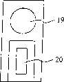
首先参照图1与图2,如图1所示,一假想发光二极管芯片,其中的圆形P型电极19与N型电极20配置在一正方形芯片表面的对角线上,此二电极互相接触,且与芯片边缘相切,若此二电极的半径皆为R,则此芯片的面积约为11.66R2。如图2所示,一假想发光二极管芯片,其中的圆形P型电极19与N型电极20并排配置在一长方形芯片的纵向,此二电极互相接触,且与芯片边缘相切,若此二电极的半径皆为R,则此芯片的面积约为8R2。因而,图2所示的First with reference to Fig. 1 and Fig. 2, as shown in Fig. 1, a hypothetical light-emitting diode chip, wherein circular P-
芯片的面积仅约为图1所示芯片面积的69%。由此可知,较现有发光二极管芯片中,P型电极19与N型电极20配置于正方形芯片表面的对角线上,依本发明概念,P型电极19与N型电极20在长方形芯片表面的纵向并排,能够减小发光二极管芯片的面积。The area of the chip is only about 69% of the area of the chip shown in FIG. 1 . It can be seen that, compared with the existing light-emitting diode chip, the P-
如图3与图4所示,其表示本发明一实施侈1的发光二极管芯片,本实施例中,发光二极管芯片包含由蓝宝石形成的一长方形绝缘衬底10、形成在绝缘衬底10上的一氮化镓晶体生长层11、形成在氮化镓晶体生长层11上的一氮化镓缓冲层12、形成在缓冲层12上的一n型氮化镓接触层13、形成在n型氮化镓接触层13上的一n型氮化铝镓束缚层14、形成在n型氮化铝镓束缚层14上的一氮化铟镓多重量子阱发光层15、形成在发光层15上的一p型氮化铝镓束缚层16、形成在p型氮化铝镓束缚层16上的一p型氮化镓接触层17、形成在p型氮化镓接触层17上的一氧化铟锡透明导电层18,其中一部份以蚀刻方式除去,以露出部分p型氮化谅接触层17,形成在p型氮化镓接触层17的该露出部分上的一p型Ti/Al前电极19,并使前电极19与透明导电层18接触,又由于蓝宝石不导电,故须将发光二极管适当地蚀刻至n型氮化镓接触层13,然后,在n氮化镓接触层13,然后在n型氮化镓接触层13上形成一n型Ti/Al后电极20,P型电极19与N型电极20并排在图3所示的长方形芯片表面的纵向,且皆与芯片边缘保持一适当距离d1,例如150微米,以免因电极未适当对正而产主任何不良后果,电极19与N型电极20之间也保持一适当距离d2,例如50微米,以免此两电极之间产生短路的不良后果;由此可知,现有发光二极管芯片中的电极19与N型电极20配置在正方形芯片表面的对角线上,而本发明中,P型电极19与N型电极20在长方形芯片表面的纵向排列,两者相比较,本发明能够减小发光二极管芯片的面积。As shown in Fig. 3 and Fig. 4, it represents a light-emitting diode chip of an embodiment of the present invention. In this embodiment, the light-emitting diode chip includes a rectangular insulating
如图5所示,其为本发明另一实施例中发光二极管芯片的俯视图,其与图3与图4所示发光二极管芯片的差异在于:N型电极20,在图5中左右二侧皆保留未经蚀刻的发光区域,以在减小发光二极管的芯片面积与增大其发光面积之间取得一恰当的平衡点。As shown in FIG. 5 , it is a top view of a light emitting diode chip in another embodiment of the present invention. The difference between it and the light emitting diode chip shown in FIG. 3 and FIG. The unetched light-emitting area is reserved to achieve a proper balance between reducing the chip area of the LED and increasing the light-emitting area.
本技术领域中的一般人士可轻易了解,绝缘衬底10可包含选自于蓝宝石、LIGaO3,及LiAlO3,所构成材料群组中的一种材料;晶体生长层11可包含选自于GaN,AlmGa1-mN,其中,0≤m≤1、及InnGa1-nN,其中,0≤n≤1,所构成材料群组中的一种材料;n型缓冲层12可由GaN材料制成;n型接触层13可包含选自于GaN与AlGaN所构成材料群组中的一种材料;n型束缚层14包含AlxGa1-xN,其中,0≤x≤1;氮化铟镓多重量子阱发光层15包含r个氮化铟镓量子阱与r+1个氮化铟镓间隔层,使得每一个氮化铟镓量子阱上下二侧皆有一氮化铟镓间隔层,其中,r≥1,每一氮化铟镓量子阱由IneGa1-eN构成,每一氮化铟镓间隔层由InfGa1-fN构成,且0≤e<f≤1,p型束缚层16可包含AlzGa1-zN,其中,0≤z≤1;p型接触层17可包含选自于GaN与AlGaN所构成材料群组中的一种材料,p型电极19可包含选自于Ti/Al、Cr/Al、Nd/Al、Pd/Al、TiN、TiWNx、Zr/Al、Hf/Al、Al、Zr以及Sc构成材料群组中的一种材料,n型电极20可包含选自于Ti/Al、Cr/Al、Nd/Al、Pd/Al、TiN、TiWNx、Zr/Al、Hf/Al、Al、Zr以及Sc构成材料群组中的一种材料。Those skilled in the art can easily understand that the insulating substrate 10 may comprise a material selected from the group consisting of sapphire, LIGaO3 , and LiAlO3 ; the crystal growth layer 11 may comprise a material selected from the group consisting of GaN , Alm Ga1-m N, wherein, 0≤m≤1, and Inn Ga1-n N, wherein, 0≤n≤1, a material in the material group formed; n-type buffer layer 12 It can be made of GaN material; the n-type contact layer 13 can include a material selected from the material group consisting of GaN and AlGaN; the n-type bound layer 14 includes Alx Ga1-x N, where 0≤x≤ 1; InGaN multiple quantum well light-emitting layer 15 includes r InGaN quantum wells and r+1 InGaN spacers, so that each InGaN quantum well has an InGaN quantum well on the upper and lower sides Gallium spacer, wherein, r≥1, each indium gallium nitride quantum well is composed of Ine Ga1-e N, each indium gallium nitride spacer is composed of Inf Ga1-f N, and 0≤e <f≤1, the p-type pinning layer 16 may comprise Alz Ga1-z N, wherein, 0≤z≤1; the p-type contact layer 17 may comprise a material selected from the group consisting of GaN and AlGaN material, the p-type electrode 19 may comprise a material selected from the group consisting of Ti/Al, Cr/Al, Nd/Al, Pd/Al, TiN, TiWNx, Zr/Al, Hf/Al, Al, Zr and Sc A kind of material, n-type electrode 20 can comprise and be selected from Ti/Al, Cr/Al, Nd/Al, Pd/Al, TiN, TiWNx, Zr/Al, Hf/Al, Al, Zr and Sc constitute material group one of the materials.
与现有技术相比,本发明具有如下效果:Compared with the prior art, the present invention has the following effects:
P型Ti/Al前电极19与p型接触层17间形成肖特基(Schottky)接触,因而在前电极19的正下方实质上不产主电流,自前电极19送出的电流经透明导电层18,流至发光层15,产生发光作用。这样,由于能够避免在不透光的前电极19的正下方产生发光作用,故能够提高发光效率。A Schottky (Schottky) contact is formed between the p-type Ti/
以上所述,仅为用实施例以方便说明本发明的特征,本发明的范围不限于此实施例,凡依本发明所做的任何变更,皆属本发明的保护范围。例如,该实施例中的氮化铟镓多重量子阱发光层15可以本技术领域中普通人员熟知的单一量子阱结构取代,或以纯氮化铟镓发光层取代;又例如,省除晶体生长层11与/或氮化镓缓冲层12,亦显然不脱离本发明的保护与范围。The above descriptions are only examples to illustrate the features of the present invention. The scope of the present invention is not limited to the examples. Any changes made according to the present invention are within the scope of protection of the present invention. For example, the InGaN multiple quantum well light-emitting
Claims (9)
Priority Applications (1)
| Application Number | Priority Date | Filing Date | Title |
|---|---|---|---|
| CNB991191536ACN1134849C (en) | 1999-09-20 | 1999-09-20 | led |
Applications Claiming Priority (1)
| Application Number | Priority Date | Filing Date | Title |
|---|---|---|---|
| CNB991191536ACN1134849C (en) | 1999-09-20 | 1999-09-20 | led |
Publications (2)
| Publication Number | Publication Date |
|---|---|
| CN1289152A CN1289152A (en) | 2001-03-28 |
| CN1134849Ctrue CN1134849C (en) | 2004-01-14 |
Family
ID=5280731
Family Applications (1)
| Application Number | Title | Priority Date | Filing Date |
|---|---|---|---|
| CNB991191536AExpired - LifetimeCN1134849C (en) | 1999-09-20 | 1999-09-20 | led |
Country Status (1)
| Country | Link |
|---|---|
| CN (1) | CN1134849C (en) |
Cited By (1)
| Publication number | Priority date | Publication date | Assignee | Title |
|---|---|---|---|---|
| CN1945865B (en)* | 2005-10-07 | 2010-05-12 | 三星电机株式会社 | Nitride-based semiconductor light-emitting diode and manufacturing method thereof |
Families Citing this family (12)
| Publication number | Priority date | Publication date | Assignee | Title |
|---|---|---|---|---|
| JP4023121B2 (en)* | 2001-09-06 | 2007-12-19 | 豊田合成株式会社 | N-type electrode, group III nitride compound semiconductor device, method for manufacturing n-type electrode, and method for manufacturing group III nitride compound semiconductor device |
| ATE500616T1 (en)* | 2002-08-29 | 2011-03-15 | Seoul Semiconductor Co Ltd | LIGHT EMITTING COMPONENT WITH LIGHT EMITTING DIODES |
| CN1316567C (en)* | 2003-04-16 | 2007-05-16 | 方大集团股份有限公司 | Preparation f green light fallium nitride base LED epitaxial wafer by adopting multiquantum well |
| KR100826424B1 (en)* | 2003-04-21 | 2008-04-29 | 삼성전기주식회사 | Semiconductor light emitting diode and method of manufacturing the same |
| CN100369276C (en)* | 2004-09-06 | 2008-02-13 | 璨圆光电股份有限公司 | The structure of light-emitting diodes |
| CN100442547C (en)* | 2004-09-06 | 2008-12-10 | 璨圆光电股份有限公司 | Gallium nitride series light-emitting diode with low-temperature growth low-resistance P type contact layer |
| CN100342559C (en)* | 2004-09-06 | 2007-10-10 | 璨圆光电股份有限公司 | Gallium nitride-based light-emitting diode manufacturing method |
| CN100336235C (en)* | 2004-09-06 | 2007-09-05 | 璨圆光电股份有限公司 | Gallium nitride-based light-emitting diode structure |
| CN100336236C (en)* | 2004-09-06 | 2007-09-05 | 璨圆光电股份有限公司 | LED structure |
| CN100392881C (en)* | 2005-06-23 | 2008-06-04 | 华南师范大学 | A kind of GaN-based LED epitaxial wafer and its preparation method |
| CN100433381C (en)* | 2005-08-02 | 2008-11-12 | 璨圆光电股份有限公司 | Flip chip type light emitting diode packaging structure and light emitting diode chip |
| TWI705581B (en)* | 2016-09-09 | 2020-09-21 | 晶元光電股份有限公司 | Light-emitting device and manufacturing method thereof |
- 1999
- 1999-09-20CNCNB991191536Apatent/CN1134849C/ennot_activeExpired - Lifetime
Cited By (1)
| Publication number | Priority date | Publication date | Assignee | Title |
|---|---|---|---|---|
| CN1945865B (en)* | 2005-10-07 | 2010-05-12 | 三星电机株式会社 | Nitride-based semiconductor light-emitting diode and manufacturing method thereof |
Also Published As
| Publication number | Publication date |
|---|---|
| CN1289152A (en) | 2001-03-28 |
Similar Documents
| Publication | Publication Date | Title |
|---|---|---|
| US9240433B2 (en) | Light emitting device | |
| CN102983129B (en) | Luminescent device | |
| CN102005465B (en) | Light emitting device and light emitting device package having the same | |
| EP2402995B1 (en) | Light emitting device and light unit | |
| CN102751410B (en) | LED (Light Emitting Diode) chip provided with stepped current blocking structure and fabricating method thereof | |
| CN102347414B (en) | Light emitting device | |
| CN102222744B (en) | Luminescent device and light emitting device package | |
| US8022430B2 (en) | Nitride-based compound semiconductor light-emitting device | |
| EP2455987A2 (en) | Light emitting device and lighting system having the same | |
| CN101075656A (en) | Nitride-based semiconductor light emitting diode | |
| CN104112757B (en) | Luminescent device, light emitting device package, the manufacture method and illuminator of luminescent device | |
| CN102832305B (en) | Luminescent device | |
| CN1134849C (en) | led | |
| CN102709417A (en) | Light emitting device and method for manufacturing the same | |
| CN114497300B (en) | Light emitting diode and light emitting device | |
| CN100380697C (en) | Group III Nitride Light Emitting Devices | |
| CN1353466A (en) | Light Emitting Diodes with Reverse Tunneling Layer | |
| CN102208509B (en) | Light emitting device, method for fabricating light emitting device, and light emitting device package | |
| CN220324473U (en) | Flip-chip light-emitting element and light-emitting device | |
| KR101978632B1 (en) | Light emitting device | |
| US10014259B2 (en) | Light emitting device, light emitting device package comprising light emitting device, and light emitting apparatus comprising light emitting device package | |
| CN1134848C (en) | Light emitting diode | |
| CN1677698A (en) | High-efficiency nitride-based light-emitting element | |
| CN1178304C (en) | InGaN Light Emitting Diodes | |
| KR102034710B1 (en) | Light Emitting Device |
Legal Events
| Date | Code | Title | Description |
|---|---|---|---|
| C10 | Entry into substantive examination | ||
| SE01 | Entry into force of request for substantive examination | ||
| C10 | Entry into substantive examination | ||
| SE01 | Entry into force of request for substantive examination | ||
| C06 | Publication | ||
| PB01 | Publication | ||
| C14 | Grant of patent or utility model | ||
| GR01 | Patent grant | ||
| CX01 | Expiry of patent term | Granted publication date:20040114 | |
| CX01 | Expiry of patent term |