CN1134601A - Organic Chip Carriers for Wire Bonded Chips - Google Patents
Organic Chip Carriers for Wire Bonded ChipsDownload PDFInfo
- Publication number
- CN1134601A CN1134601ACN96102102ACN96102102ACN1134601ACN 1134601 ACN1134601 ACN 1134601ACN 96102102 ACN96102102 ACN 96102102ACN 96102102 ACN96102102 ACN 96102102ACN 1134601 ACN1134601 ACN 1134601A
- Authority
- CN
- China
- Prior art keywords
- layer
- chip
- chip carrier
- pads
- extending
- Prior art date
- Legal status (The legal status is an assumption and is not a legal conclusion. Google has not performed a legal analysis and makes no representation as to the accuracy of the status listed.)
- Granted
Links
Images


Classifications
- H—ELECTRICITY
- H05—ELECTRIC TECHNIQUES NOT OTHERWISE PROVIDED FOR
- H05K—PRINTED CIRCUITS; CASINGS OR CONSTRUCTIONAL DETAILS OF ELECTRIC APPARATUS; MANUFACTURE OF ASSEMBLAGES OF ELECTRICAL COMPONENTS
- H05K1/00—Printed circuits
- H05K1/02—Details
- H05K1/0201—Thermal arrangements, e.g. for cooling, heating or preventing overheating
- H05K1/0203—Cooling of mounted components
- H05K1/021—Components thermally connected to metal substrates or heat-sinks by insert mounting
- H—ELECTRICITY
- H01—ELECTRIC ELEMENTS
- H01L—SEMICONDUCTOR DEVICES NOT COVERED BY CLASS H10
- H01L21/00—Processes or apparatus adapted for the manufacture or treatment of semiconductor or solid state devices or of parts thereof
- H01L21/02—Manufacture or treatment of semiconductor devices or of parts thereof
- H01L21/04—Manufacture or treatment of semiconductor devices or of parts thereof the devices having potential barriers, e.g. a PN junction, depletion layer or carrier concentration layer
- H01L21/50—Assembly of semiconductor devices using processes or apparatus not provided for in a single one of the groups H01L21/18 - H01L21/326 or H10D48/04 - H10D48/07 e.g. sealing of a cap to a base of a container
- H01L21/60—Attaching or detaching leads or other conductive members, to be used for carrying current to or from the device in operation
- H—ELECTRICITY
- H01—ELECTRIC ELEMENTS
- H01L—SEMICONDUCTOR DEVICES NOT COVERED BY CLASS H10
- H01L23/00—Details of semiconductor or other solid state devices
- H01L23/12—Mountings, e.g. non-detachable insulating substrates
- H01L23/14—Mountings, e.g. non-detachable insulating substrates characterised by the material or its electrical properties
- H01L23/145—Organic substrates, e.g. plastic
- H—ELECTRICITY
- H01—ELECTRIC ELEMENTS
- H01L—SEMICONDUCTOR DEVICES NOT COVERED BY CLASS H10
- H01L23/00—Details of semiconductor or other solid state devices
- H01L23/34—Arrangements for cooling, heating, ventilating or temperature compensation ; Temperature sensing arrangements
- H01L23/36—Selection of materials, or shaping, to facilitate cooling or heating, e.g. heatsinks
- H01L23/367—Cooling facilitated by shape of device
- H01L23/3677—Wire-like or pin-like cooling fins or heat sinks
- H—ELECTRICITY
- H01—ELECTRIC ELEMENTS
- H01L—SEMICONDUCTOR DEVICES NOT COVERED BY CLASS H10
- H01L23/00—Details of semiconductor or other solid state devices
- H01L23/48—Arrangements for conducting electric current to or from the solid state body in operation, e.g. leads, terminal arrangements ; Selection of materials therefor
- H01L23/488—Arrangements for conducting electric current to or from the solid state body in operation, e.g. leads, terminal arrangements ; Selection of materials therefor consisting of soldered or bonded constructions
- H01L23/498—Leads, i.e. metallisations or lead-frames on insulating substrates, e.g. chip carriers
- H01L23/49822—Multilayer substrates
- H—ELECTRICITY
- H01—ELECTRIC ELEMENTS
- H01L—SEMICONDUCTOR DEVICES NOT COVERED BY CLASS H10
- H01L2224/00—Indexing scheme for arrangements for connecting or disconnecting semiconductor or solid-state bodies and methods related thereto as covered by H01L24/00
- H01L2224/01—Means for bonding being attached to, or being formed on, the surface to be connected, e.g. chip-to-package, die-attach, "first-level" interconnects; Manufacturing methods related thereto
- H01L2224/42—Wire connectors; Manufacturing methods related thereto
- H01L2224/44—Structure, shape, material or disposition of the wire connectors prior to the connecting process
- H01L2224/45—Structure, shape, material or disposition of the wire connectors prior to the connecting process of an individual wire connector
- H01L2224/45001—Core members of the connector
- H01L2224/45099—Material
- H01L2224/451—Material with a principal constituent of the material being a metal or a metalloid, e.g. boron (B), silicon (Si), germanium (Ge), arsenic (As), antimony (Sb), tellurium (Te) and polonium (Po), and alloys thereof
- H01L2224/45138—Material with a principal constituent of the material being a metal or a metalloid, e.g. boron (B), silicon (Si), germanium (Ge), arsenic (As), antimony (Sb), tellurium (Te) and polonium (Po), and alloys thereof the principal constituent melting at a temperature of greater than or equal to 950°C and less than 1550°C
- H01L2224/45144—Gold (Au) as principal constituent
- H—ELECTRICITY
- H01—ELECTRIC ELEMENTS
- H01L—SEMICONDUCTOR DEVICES NOT COVERED BY CLASS H10
- H01L2224/00—Indexing scheme for arrangements for connecting or disconnecting semiconductor or solid-state bodies and methods related thereto as covered by H01L24/00
- H01L2224/01—Means for bonding being attached to, or being formed on, the surface to be connected, e.g. chip-to-package, die-attach, "first-level" interconnects; Manufacturing methods related thereto
- H01L2224/42—Wire connectors; Manufacturing methods related thereto
- H01L2224/47—Structure, shape, material or disposition of the wire connectors after the connecting process
- H01L2224/48—Structure, shape, material or disposition of the wire connectors after the connecting process of an individual wire connector
- H01L2224/4805—Shape
- H01L2224/4809—Loop shape
- H01L2224/48091—Arched
- H—ELECTRICITY
- H01—ELECTRIC ELEMENTS
- H01L—SEMICONDUCTOR DEVICES NOT COVERED BY CLASS H10
- H01L24/00—Arrangements for connecting or disconnecting semiconductor or solid-state bodies; Methods or apparatus related thereto
- H01L24/01—Means for bonding being attached to, or being formed on, the surface to be connected, e.g. chip-to-package, die-attach, "first-level" interconnects; Manufacturing methods related thereto
- H01L24/42—Wire connectors; Manufacturing methods related thereto
- H01L24/44—Structure, shape, material or disposition of the wire connectors prior to the connecting process
- H01L24/45—Structure, shape, material or disposition of the wire connectors prior to the connecting process of an individual wire connector
- H—ELECTRICITY
- H01—ELECTRIC ELEMENTS
- H01L—SEMICONDUCTOR DEVICES NOT COVERED BY CLASS H10
- H01L24/00—Arrangements for connecting or disconnecting semiconductor or solid-state bodies; Methods or apparatus related thereto
- H01L24/01—Means for bonding being attached to, or being formed on, the surface to be connected, e.g. chip-to-package, die-attach, "first-level" interconnects; Manufacturing methods related thereto
- H01L24/42—Wire connectors; Manufacturing methods related thereto
- H01L24/47—Structure, shape, material or disposition of the wire connectors after the connecting process
- H01L24/48—Structure, shape, material or disposition of the wire connectors after the connecting process of an individual wire connector
- H—ELECTRICITY
- H01—ELECTRIC ELEMENTS
- H01L—SEMICONDUCTOR DEVICES NOT COVERED BY CLASS H10
- H01L2924/00—Indexing scheme for arrangements or methods for connecting or disconnecting semiconductor or solid-state bodies as covered by H01L24/00
- H01L2924/0001—Technical content checked by a classifier
- H01L2924/00014—Technical content checked by a classifier the subject-matter covered by the group, the symbol of which is combined with the symbol of this group, being disclosed without further technical details
- H—ELECTRICITY
- H01—ELECTRIC ELEMENTS
- H01L—SEMICONDUCTOR DEVICES NOT COVERED BY CLASS H10
- H01L2924/00—Indexing scheme for arrangements or methods for connecting or disconnecting semiconductor or solid-state bodies as covered by H01L24/00
- H01L2924/01—Chemical elements
- H01L2924/01046—Palladium [Pd]
- H—ELECTRICITY
- H01—ELECTRIC ELEMENTS
- H01L—SEMICONDUCTOR DEVICES NOT COVERED BY CLASS H10
- H01L2924/00—Indexing scheme for arrangements or methods for connecting or disconnecting semiconductor or solid-state bodies as covered by H01L24/00
- H01L2924/01—Chemical elements
- H01L2924/01078—Platinum [Pt]
- H—ELECTRICITY
- H01—ELECTRIC ELEMENTS
- H01L—SEMICONDUCTOR DEVICES NOT COVERED BY CLASS H10
- H01L2924/00—Indexing scheme for arrangements or methods for connecting or disconnecting semiconductor or solid-state bodies as covered by H01L24/00
- H01L2924/01—Chemical elements
- H01L2924/01079—Gold [Au]
- H—ELECTRICITY
- H01—ELECTRIC ELEMENTS
- H01L—SEMICONDUCTOR DEVICES NOT COVERED BY CLASS H10
- H01L2924/00—Indexing scheme for arrangements or methods for connecting or disconnecting semiconductor or solid-state bodies as covered by H01L24/00
- H01L2924/10—Details of semiconductor or other solid state devices to be connected
- H01L2924/11—Device type
- H01L2924/12—Passive devices, e.g. 2 terminal devices
- H01L2924/1204—Optical Diode
- H01L2924/12042—LASER
- H—ELECTRICITY
- H01—ELECTRIC ELEMENTS
- H01L—SEMICONDUCTOR DEVICES NOT COVERED BY CLASS H10
- H01L2924/00—Indexing scheme for arrangements or methods for connecting or disconnecting semiconductor or solid-state bodies as covered by H01L24/00
- H01L2924/10—Details of semiconductor or other solid state devices to be connected
- H01L2924/11—Device type
- H01L2924/12—Passive devices, e.g. 2 terminal devices
- H01L2924/1204—Optical Diode
- H01L2924/12044—OLED
- H—ELECTRICITY
- H01—ELECTRIC ELEMENTS
- H01L—SEMICONDUCTOR DEVICES NOT COVERED BY CLASS H10
- H01L2924/00—Indexing scheme for arrangements or methods for connecting or disconnecting semiconductor or solid-state bodies as covered by H01L24/00
- H01L2924/10—Details of semiconductor or other solid state devices to be connected
- H01L2924/11—Device type
- H01L2924/14—Integrated circuits
- H—ELECTRICITY
- H01—ELECTRIC ELEMENTS
- H01L—SEMICONDUCTOR DEVICES NOT COVERED BY CLASS H10
- H01L2924/00—Indexing scheme for arrangements or methods for connecting or disconnecting semiconductor or solid-state bodies as covered by H01L24/00
- H01L2924/15—Details of package parts other than the semiconductor or other solid state devices to be connected
- H01L2924/151—Die mounting substrate
- H01L2924/1515—Shape
- H01L2924/15153—Shape the die mounting substrate comprising a recess for hosting the device
- H—ELECTRICITY
- H01—ELECTRIC ELEMENTS
- H01L—SEMICONDUCTOR DEVICES NOT COVERED BY CLASS H10
- H01L2924/00—Indexing scheme for arrangements or methods for connecting or disconnecting semiconductor or solid-state bodies as covered by H01L24/00
- H01L2924/15—Details of package parts other than the semiconductor or other solid state devices to be connected
- H01L2924/151—Die mounting substrate
- H01L2924/15165—Monolayer substrate
- H—ELECTRICITY
- H01—ELECTRIC ELEMENTS
- H01L—SEMICONDUCTOR DEVICES NOT COVERED BY CLASS H10
- H01L2924/00—Indexing scheme for arrangements or methods for connecting or disconnecting semiconductor or solid-state bodies as covered by H01L24/00
- H01L2924/15—Details of package parts other than the semiconductor or other solid state devices to be connected
- H01L2924/151—Die mounting substrate
- H01L2924/153—Connection portion
- H01L2924/1531—Connection portion the connection portion being formed only on the surface of the substrate opposite to the die mounting surface
- H01L2924/15311—Connection portion the connection portion being formed only on the surface of the substrate opposite to the die mounting surface being a ball array, e.g. BGA
- H—ELECTRICITY
- H01—ELECTRIC ELEMENTS
- H01L—SEMICONDUCTOR DEVICES NOT COVERED BY CLASS H10
- H01L2924/00—Indexing scheme for arrangements or methods for connecting or disconnecting semiconductor or solid-state bodies as covered by H01L24/00
- H01L2924/15—Details of package parts other than the semiconductor or other solid state devices to be connected
- H01L2924/151—Die mounting substrate
- H01L2924/153—Connection portion
- H01L2924/1532—Connection portion the connection portion being formed on the die mounting surface of the substrate
- H—ELECTRICITY
- H01—ELECTRIC ELEMENTS
- H01L—SEMICONDUCTOR DEVICES NOT COVERED BY CLASS H10
- H01L2924/00—Indexing scheme for arrangements or methods for connecting or disconnecting semiconductor or solid-state bodies as covered by H01L24/00
- H01L2924/15—Details of package parts other than the semiconductor or other solid state devices to be connected
- H01L2924/181—Encapsulation
- H—ELECTRICITY
- H05—ELECTRIC TECHNIQUES NOT OTHERWISE PROVIDED FOR
- H05K—PRINTED CIRCUITS; CASINGS OR CONSTRUCTIONAL DETAILS OF ELECTRIC APPARATUS; MANUFACTURE OF ASSEMBLAGES OF ELECTRICAL COMPONENTS
- H05K1/00—Printed circuits
- H05K1/18—Printed circuits structurally associated with non-printed electric components
- H05K1/182—Printed circuits structurally associated with non-printed electric components associated with components mounted in the printed circuit board, e.g. insert mounted components [IMC]
- H—ELECTRICITY
- H05—ELECTRIC TECHNIQUES NOT OTHERWISE PROVIDED FOR
- H05K—PRINTED CIRCUITS; CASINGS OR CONSTRUCTIONAL DETAILS OF ELECTRIC APPARATUS; MANUFACTURE OF ASSEMBLAGES OF ELECTRICAL COMPONENTS
- H05K2201/00—Indexing scheme relating to printed circuits covered by H05K1/00
- H05K2201/09—Shape and layout
- H05K2201/09009—Substrate related
- H05K2201/09127—PCB or component having an integral separable or breakable part
- H—ELECTRICITY
- H05—ELECTRIC TECHNIQUES NOT OTHERWISE PROVIDED FOR
- H05K—PRINTED CIRCUITS; CASINGS OR CONSTRUCTIONAL DETAILS OF ELECTRIC APPARATUS; MANUFACTURE OF ASSEMBLAGES OF ELECTRICAL COMPONENTS
- H05K2201/00—Indexing scheme relating to printed circuits covered by H05K1/00
- H05K2201/09—Shape and layout
- H05K2201/09818—Shape or layout details not covered by a single group of H05K2201/09009 - H05K2201/09809
- H05K2201/09981—Metallised walls
- H—ELECTRICITY
- H05—ELECTRIC TECHNIQUES NOT OTHERWISE PROVIDED FOR
- H05K—PRINTED CIRCUITS; CASINGS OR CONSTRUCTIONAL DETAILS OF ELECTRIC APPARATUS; MANUFACTURE OF ASSEMBLAGES OF ELECTRICAL COMPONENTS
- H05K2203/00—Indexing scheme relating to apparatus or processes for manufacturing printed circuits covered by H05K3/00
- H05K2203/04—Soldering or other types of metallurgic bonding
- H05K2203/049—Wire bonding
- H—ELECTRICITY
- H05—ELECTRIC TECHNIQUES NOT OTHERWISE PROVIDED FOR
- H05K—PRINTED CIRCUITS; CASINGS OR CONSTRUCTIONAL DETAILS OF ELECTRIC APPARATUS; MANUFACTURE OF ASSEMBLAGES OF ELECTRICAL COMPONENTS
- H05K3/00—Apparatus or processes for manufacturing printed circuits
- H05K3/0058—Laminating printed circuit boards onto other substrates, e.g. metallic substrates
- H05K3/0061—Laminating printed circuit boards onto other substrates, e.g. metallic substrates onto a metallic substrate, e.g. a heat sink
- Y—GENERAL TAGGING OF NEW TECHNOLOGICAL DEVELOPMENTS; GENERAL TAGGING OF CROSS-SECTIONAL TECHNOLOGIES SPANNING OVER SEVERAL SECTIONS OF THE IPC; TECHNICAL SUBJECTS COVERED BY FORMER USPC CROSS-REFERENCE ART COLLECTIONS [XRACs] AND DIGESTS
- Y10—TECHNICAL SUBJECTS COVERED BY FORMER USPC
- Y10T—TECHNICAL SUBJECTS COVERED BY FORMER US CLASSIFICATION
- Y10T29/00—Metal working
- Y10T29/49—Method of mechanical manufacture
- Y10T29/49002—Electrical device making
- Y10T29/49117—Conductor or circuit manufacturing
- Y10T29/49124—On flat or curved insulated base, e.g., printed circuit, etc.
- Y10T29/4913—Assembling to base an electrical component, e.g., capacitor, etc.
- Y—GENERAL TAGGING OF NEW TECHNOLOGICAL DEVELOPMENTS; GENERAL TAGGING OF CROSS-SECTIONAL TECHNOLOGIES SPANNING OVER SEVERAL SECTIONS OF THE IPC; TECHNICAL SUBJECTS COVERED BY FORMER USPC CROSS-REFERENCE ART COLLECTIONS [XRACs] AND DIGESTS
- Y10—TECHNICAL SUBJECTS COVERED BY FORMER USPC
- Y10T—TECHNICAL SUBJECTS COVERED BY FORMER US CLASSIFICATION
- Y10T29/00—Metal working
- Y10T29/49—Method of mechanical manufacture
- Y10T29/49002—Electrical device making
- Y10T29/49117—Conductor or circuit manufacturing
- Y10T29/49124—On flat or curved insulated base, e.g., printed circuit, etc.
- Y10T29/49155—Manufacturing circuit on or in base
Landscapes
- Engineering & Computer Science (AREA)
- Microelectronics & Electronic Packaging (AREA)
- Physics & Mathematics (AREA)
- Condensed Matter Physics & Semiconductors (AREA)
- General Physics & Mathematics (AREA)
- Computer Hardware Design (AREA)
- Power Engineering (AREA)
- Chemical & Material Sciences (AREA)
- Materials Engineering (AREA)
- Manufacturing & Machinery (AREA)
- Production Of Multi-Layered Print Wiring Board (AREA)
- Cooling Or The Like Of Semiconductors Or Solid State Devices (AREA)
- Transforming Light Signals Into Electric Signals (AREA)
- Adhesives Or Adhesive Processes (AREA)
- Structures For Mounting Electric Components On Printed Circuit Boards (AREA)
- Led Device Packages (AREA)
- Internal Circuitry In Semiconductor Integrated Circuit Devices (AREA)
- Resistance Heating (AREA)
- Wire Bonding (AREA)
- Die Bonding (AREA)
- Structure Of Printed Boards (AREA)
Abstract
Description
Translated fromChinese本发明一般涉及到用于引线连接式芯片的有机芯片载体。The present invention generally relates to organic chip carriers for wire bonded chips.
半导体集成电路器件(以下称之为半导体芯片或芯片)的电学封装方法通常是将一个或几个芯片安装在陶瓷(例如氧化铝)芯片载体衬底上,并采取引线连接的方法将各芯片上的I/O(输入/输出端)接触焊点电连接到陶瓷芯片载体衬底上相应的接触焊点上(因而也是相应的扇出电路)。然后将得到的陶瓷芯片载体安装在印刷电路板(PCB)上或印刷电路卡片(PCC)上,并从而(经由PCB或PCC上的电路)电连接到安装在PCB或PCC上的其它陶瓷芯片载体和其它电子元件上。The electrical packaging method of semiconductor integrated circuit devices (hereinafter referred to as semiconductor chips or chips) is usually to install one or several chips on a ceramic (such as alumina) chip carrier substrate, and to connect the chips on each chip by wire connection. The I/O (input/output) contact pads of the ceramic chip carrier substrate are electrically connected to corresponding contact pads on the ceramic chip carrier substrate (and thus corresponding fan-out circuits). The resulting ceramic chip carrier is then mounted on a printed circuit board (PCB) or printed circuit card (PCC) and thereby electrically connected (via circuitry on the PCB or PCC) to other ceramic chip carriers mounted on the PCB or PCC and other electronic components.
虽然上述的封装方法肯定是有用的、但采用陶瓷芯片载体衬底确实牵涉到一些限制和缺点。例如,正如人们已知的,电信号通过介电层上或二个介电层之间的引线的传播速度正比于介电层介电常数平方根的倒数。不幸的是,陶瓷的介电常数相当大,例如氧化铝的介电常数约为9,这就使陶瓷芯片载体的信号传播速度相当低,有时低得不合要求。While the packaging methods described above are certainly useful, the use of ceramic chip carrier substrates does involve some limitations and disadvantages. For example, as is known, the propagation velocity of an electrical signal through a lead on a dielectric layer or between two dielectric layers is proportional to the inverse of the square root of the dielectric constant of the dielectric layer. Unfortunately, the dielectric constant of ceramics is quite high, for example alumina has a dielectric constant of about 9, which makes the signal propagation speed of ceramic chip carriers quite low, sometimes undesirably low.
采用陶瓷芯片载体衬底还引起某些I/O限制。例如,单层陶瓷芯片载体衬底在陶瓷单层的上表面上只包含一层延伸至陶瓷单层外围附近接触焊点的扇出电路。(通常用带有连接于这些外围接触焊点的内引线的引线框来实现这种陶瓷芯片载体到PCB或PCC的电连接。)然而,当芯片I/O数目增加时,就必须增加扇出引线的数目,而且必须相应地减小各扇出引线之间的间隔,直至相邻扇出引线之间不希望有的串扰变成不可接受。而且,在陶瓷层外围附近要制作相应的大量接触焊点即使不是不可能,也变得越来越困难。这样,单层陶瓷芯片载体衬底在其处置具有大量I/0的芯片的能力方面肯定要受到限制。The use of ceramic chip carrier substrates also imposes certain I/O limitations. For example, a single layer ceramic chip carrier substrate includes only one layer of fan-out circuitry on the upper surface of the ceramic monolayer extending to contact pads near the periphery of the ceramic monolayer. (The electrical connection of this ceramic chip carrier to a PCB or PCC is usually accomplished with a lead frame with inner leads connected to these peripheral contact pads.) However, as the chip I/O count increases, fanout must be increased The number of leads, and the spacing between each fan-out lead must be reduced accordingly until the unwanted crosstalk between adjacent fan-out leads becomes unacceptable. Furthermore, it is becoming increasingly difficult, if not impossible, to produce a correspondingly large number of contact pads near the periphery of the ceramic layer. Thus, single layer ceramic chip carrier substrates are necessarily limited in their ability to handle chips with a large number of I/Os.
为适应具有相当大量I/0数目的芯片而作的努力导致了采用多层陶瓷芯片载体衬底,它采用所谓的球栅阵列(BGA)来代替引线框。这种陶瓷芯片载体衬底与单层陶瓷芯片载体衬底之间的差别在于,它们在二个或多个陶瓷层上含有二个或多个扇出电路层。重要的是,扇出电路的各层间的电互连是用机械钻制的通道孔(镀有和/或填充有导电材料)来实现的。此外,一定数目的这种孔从扇出电路层延伸到芯片载体衬底上装设有焊球(呈栅阵列状,故称球栅阵列)的底部。这些焊球要按机械方式和导电连接到PCB或PCC上各相应的可焊接的接触焊点。遗憾的是,使扇出电路各层导电互连的机械钻制的孔的直径相当大,要求扇出引线之间的间隔相当大。但这一相当大的扇出引线之间的间隔限制了这种多层陶瓷衬底芯片载体衬底所能容纳的芯片I/O的数目。Efforts to accommodate chips with relatively large I/O counts have led to the use of multilayer ceramic chip carrier substrates, which use so-called ball grid arrays (BGA) instead of lead frames. Such ceramic chip carrier substrates differ from single layer ceramic chip carrier substrates in that they contain two or more layers of fan-out circuitry on top of two or more ceramic layers. Importantly, the electrical interconnection between the layers of the fan-out circuit is accomplished using mechanically drilled via holes (plated and/or filled with conductive material). In addition, a certain number of such holes extend from the fan-out circuit layer to the bottom of the chip carrier substrate where solder balls (in a grid array shape, so called ball grid array) are installed. These solder balls are mechanically and electrically connected to respective solderable contact pads on the PCB or PCC. Unfortunately, the diameter of the mechanically drilled holes that electrically interconnect the layers of the fan-out circuit is relatively large, requiring a relatively large spacing between the fan-out leads. But this relatively large spacing between the fanout leads limits the number of chip I/Os that can be accommodated by such a multilayer ceramic substrate chip carrier substrate.
为封装具有相当大数目芯片I/0的芯片所作的其它努力导致采用多层陶瓷衬底中的多层坑。(此处所谓的“坑”表示衬底中的一个凹陷处而不是贯穿衬底厚度的孔)。当采用这种封装结构时,芯片面朝上地安装在多层坑的底部。引线从芯片上表面的I/O接触焊点延伸到构成多层坑的不同层的多层陶瓷衬底的不同层的各个暴露的上表面上的接触焊点。尽管这种结构确实能够容纳相当大量的芯片I/O,它也确实使从芯片延伸到多层坑上层的引线相当长。结果,相应电信号的“飞行时间”就不希望有地增加了。Other efforts to package chips with a significant number of chip I/Os have resulted in the use of multiple layers of wells in multilayer ceramic substrates. (By "pit" here we mean a depression in the substrate rather than a hole through the thickness of the substrate). When using this package structure, the chip is mounted face-up on the bottom of the multi-layer pit. Leads extend from the I/O contact pads on the upper surface of the chip to contact pads on respective exposed upper surfaces of the different layers of the multilayer ceramic substrate constituting the different layers of the multilayer well. While this structure does accommodate a relatively large number of chip I/Os, it also does make the leads extending from the chip to the upper layers of the multi-layer well relatively long. As a result, the "time of flight" of the corresponding electrical signal is undesirably increased.
陶瓷芯片载体衬底就其热耗散能力来说也受到限制。例如,在带有位于多层坑底部的芯片的多层陶瓷芯片载体的情况下,通一常是用直接于坑的下方提供热沉(heat sink)的方法来获得热耗散。但这意味着芯片产生的热在到达热沉之前必须传递坑底部的陶瓷层。结果,热耗散速率受到限制。Ceramic chip carrier substrates are also limited in their ability to dissipate heat. For example, in the case of a multilayer ceramic chip carrier with chips at the bottom of a multilayer well, heat dissipation is usually achieved by providing a heat sink directly below the well. But this means that the heat generated by the chip has to travel to the ceramic layer at the bottom of the pit before reaching the heat sink. As a result, the rate of heat dissipation is limited.
于是,开发芯片载体的人们就希望有一种芯片载体能够:(1)具有相当高的电信号传播速度;(2)能容纳相当大量I/O的芯片同时又无需机械钻制的孔来互连扇出电路的不同层;(3)具有相当短的“飞行时间”;以及(4)具有相当高的热耗散速率。但迄今未能成功。Therefore, people who develop chip carriers hope to have a chip carrier that can: (1) have a relatively high speed of electrical signal propagation; different layers of fanout circuitry; (3) have a relatively short "time of flight"; and (4) have a relatively high rate of heat dissipation. But so far without success.
本发明涉及到一种芯片载体,它:(1)具有相当高的电信号传播速度;(2)能容纳相当大量I/O的芯片同时又无需机械钻制的孔来互连扇出电路的不同层;(3)免去了采用相当长的引线,从而获得了相当短的“飞行时间”;以及(4)获得了相当高的热耗散速率。The present invention relates to a chip carrier that: (1) has a relatively high electrical signal propagation velocity; (2) can accommodate a chip with a relatively large number of I/Os without the need for mechanically drilled holes to interconnect fan-out circuits different layers; (3) avoiding the use of relatively long leads, thereby obtaining a relatively short "time of flight"; and (4) obtaining a relatively high rate of heat dissipation.
重要的是,本发明的芯片载体采用了诸如以FR4和DriClad商标出售的环氧/玻璃配方的有机介电材料来代替陶瓷介电材料。这些有机材料的介电常数相当低,例如FR4的介电常数为4.0。结果,本发明的芯片载体就具有相当高的电信号传播速度。Importantly, the chip carrier of the present invention employs organic dielectric materials such as epoxy/glass formulations sold under the trademarks FR4 and DriClad instead of ceramic dielectric materials. The dielectric constant of these organic materials is quite low, for example FR4 has a dielectric constant of 4.0. As a result, the chip carrier of the present invention has a relatively high electrical signal propagation speed.
本发明的芯片载体还采用一个用作薄膜再分布层(FRL)的有机可光学成像的介电层。亦即,此特殊的有机介电层对光很灵敏,并且正如光抗蚀剂那样可用掩模方便地选择性曝光及显影,以便在可光学成像介电层中形成通道孔(此处称之为光学通道以区别于机械钻制的通道孔)。重要的是,这些光学通道可容易地做成直径远远小于常规机械钻孔技术所形成的通道的直径。例如,常规钻制通道孔的直径通常不小于约12密尔(0.012英寸),而光学通道的直径可小于例如2密尔(0.002英寸)。结果,当这种可光学成像介电层结合到本发明的芯片载体中的时候,就可以使扇出电路的二个(或更多个)层互连而不必将扇出引线之间的间隔限制到采用机械钻制孔那样的程度。结果,本发明的芯片载体就可容纳具有比常规陶瓷芯片载体所能容纳的更多的I/O数目的芯片。The chip carrier of the present invention also employs an organic photoimageable dielectric layer as a thin film redistribution layer (FRL). That is, this particular organic dielectric layer is sensitive to light and, like a photoresist, can be selectively exposed and developed with a mask conveniently to form via holes (referred to herein as for optical access to distinguish it from mechanically drilled access holes). Importantly, these optical channels can easily be made in diameters much smaller than those formed by conventional mechanical drilling techniques. For example, the diameter of a conventional drilled via hole is typically not less than about 12 mils (0.012 inches), while the diameter of an optical channel may be less than, for example, 2 mils (0.002 inches). As a result, when such a photoimageable dielectric layer is incorporated into the chip carrier of the present invention, it is possible to interconnect two (or more) layers of fan-out circuitry without increasing the spacing between fan-out leads. Limited to the extent that a hole is made with a mechanical drill. As a result, the chip carrier of the present invention can accommodate chips having a greater number of I/Os than conventional ceramic chip carriers can accommodate.
本发明的芯片载体还采用一个单层坑(single-tiered cavity)来容纳一个芯片而不是采用多层坑。结果就避免了相当长的引线连接。因此,本发明的芯片载体可得到相当短的相应电信号的“飞行时间”。The chip carrier of the present invention also uses a single-tiered cavity to accommodate a chip instead of multiple layers of cavity. As a result, relatively long lead connections are avoided. Accordingly, the chip carrier of the present invention achieves a relatively short "time of flight" of the corresponding electrical signal.
在本发明的一个实施例中,热通道孔提供在单层坑之下方,延伸至芯片载体的底部,以便将芯片产生的热排出到大气中。在另一实施例中,将热沉直接提供在热通道孔下方以进一步增强热耗散。在又一个实施例中,芯片载体包含一个用作热沉的金属(例如铜)层,而且单层坑的深度延伸到甚至进入金属层。这就在坑中的芯片与热沉之间导致直接的物理接触,引起更大的热耗散。In one embodiment of the present invention, thermal via holes are provided under the single layer wells, extending to the bottom of the chip carrier, in order to discharge the heat generated by the chip to the atmosphere. In another embodiment, a heat sink is provided directly below the thermal via holes to further enhance heat dissipation. In yet another embodiment, the chip carrier includes a metal (eg, copper) layer that acts as a heat sink, and the depth of the monolayer pit extends even into the metal layer. This results in direct physical contact between the chip in the cavity and the heat sink, causing greater heat dissipation.
在另一实施例中,本发明的芯片载体至少包括二个有机层,其间夹有一个接地平面。同这一实施例相关的单层坑的深度至少延伸至接地平面。重要的是,本实施例还包含一个几乎连续的金属环围绕着坑的侧壁并按垂直方向延伸至芯片载体的上表面。由于此金属环使得有可能容易与接地平面导电接触同时又无需延伸至接地平面的机械钻制的通道孔,故此金属环的存在是有利的。结果就可有利地减小扇出引线之间的间隔。In another embodiment, the chip carrier of the present invention includes at least two organic layers with a ground plane sandwiched therebetween. The depth of the single layer pit associated with this embodiment extends at least as far as the ground plane. Importantly, this embodiment also includes a nearly continuous metal ring surrounding the sidewalls of the cavity and extending vertically to the upper surface of the chip carrier. The presence of this metal ring is advantageous since it makes possible easy conductive contact with the ground plane while eliminating the need for mechanically drilled via holes extending to the ground plane. As a result, the spacing between the fan-out leads can be advantageously reduced.
参照附图来描述本发明,在这些附图中:The invention is described with reference to the accompanying drawings, in which:
图1是本发明芯片载体第一实施例的剖面图;Fig. 1 is the sectional view of the first embodiment of the chip carrier of the present invention;
图2是本发明芯片载体第二实施例的剖面图;Fig. 2 is the sectional view of the second embodiment of the chip carrier of the present invention;
图3是本发明芯片载体第三实施例的剖面图;3 is a cross-sectional view of a third embodiment of the chip carrier of the present invention;
图4是本发明芯片载体第四实施例的剖面图;4 is a cross-sectional view of a fourth embodiment of a chip carrier of the present invention;
图5是本发明芯片载体第五实施例的剖面图;以及5 is a cross-sectional view of a fifth embodiment of the chip carrier of the present invention; and
图6是衬底的俯视图,示出了用于制造本发明芯片载体第五实施例的工序。Fig. 6 is a top view of a substrate showing a process for manufacturing a fifth embodiment of a chip carrier of the present invention.
本发明涉及到一种用于引线连接式芯片的芯片载体,这种载体(1)具有相当高的电信号传播速度;(2)容易容纳相当大量的I/O的芯片;(3)无需长的引线连接从而获得相当短的电信号传过引线的“飞行时间”;以及(4)获得了相当高的热耗散速率。The present invention relates to a chip carrier for wire-bonded chips, which (1) has a relatively high electrical signal propagation velocity; (2) easily accommodates a chip with a relatively large number of I/Os; (3) does not require a long lead connections to obtain a relatively short "time of flight" for electrical signals to travel through the leads; and (4) obtain a relatively high rate of heat dissipation.
如上所述,本发明的芯片载体由于采用了诸如以商标FR4和DriClad出售的环氧/玻璃配方的有机材料来代替陶瓷材料而获得了相当高的电传播速度。本发明的芯片载体由于至少采用了一种其中形成了光学通道的有机可光学成像介电层作为薄膜再分布层(FRL)以电互连扇出电路的二个(或更多个)层,故还易于容纳相当大量I/O的芯片。本发明的芯片载体避免了相当长的引线连接,因而传过引线连接的电信号获得了相当短的“飞行时间”,这是由于采用了单层坑而不是多层坑来容纳芯片。而且,本发明的芯片载体的某些实施例还含有例如直接位于芯片之下的热通道或金属材料层来增强热传输。As mentioned above, the chip carrier of the present invention achieves a relatively high electrical propagation velocity due to the use of organic materials such as epoxy/glass formulations sold under the trademarks FR4 and DriClad instead of ceramic materials. The chip carrier of the present invention employs at least one organic photoimageable dielectric layer in which optical channels are formed as a film redistribution layer (FRL) to electrically interconnect two (or more) layers of fan-out circuits, Therefore, it is also easy to accommodate chips with a relatively large number of I/Os. The chip carrier of the present invention avoids relatively long wire connections and thus obtains a relatively short "time of flight" for electrical signals passing through the wire connections due to the use of a single layer of wells rather than multiple layers of wells to accommodate the chips. Furthermore, certain embodiments of the chip carrier of the present invention also contain, for example, thermal vias or layers of metallic material directly under the chip to enhance heat transfer.
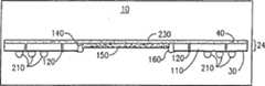
现参照图1,本发明芯片载体10的第一实施例包括一个带有相对表面30和40的芯片载体衬底20。此衬底20还包含多个(例如三个)叠层有机介电层50、60和70,它们由例如以商标FR4和DriClad出售的环氧/玻璃配方组成。虽然在图1中未清楚地示出,此有机介电层50用来支持例如由铜构成的扇出电路层80。在有机介电层50和60之间夹有一层90,它由导电材料例如铜构成,用作电源面。在有机介电层60和70之间夹有另一层100,它由导电材料例如铜组成,用作接地面。Referring now to FIG. 1 , a first embodiment of a
有机介电层50、60和70的厚度范围为约2密尔到约20密尔。小于约2密尔的厚度由于对应的有机介电层不合要求地脆弱、不可靠且难以处置而不可取。大于约20密尔的厚度则由于一般不需要如此厚的介电层以及在如此厚的层中难以钻制通道孔因而也不可取。The thickness of organic dielectric layers 50, 60 and 70 ranges from about 2 mils to about 20 mils. Thicknesses of less than about 2 mils are undesirable because the corresponding organic dielectric layers are undesirably fragile, unreliable, and difficult to handle. Thicknesses greater than about 20 mils are also undesirable due to the general need for such thick dielectric layers and the difficulty of drilling via holes in such thick layers.
各导电材料层80(扇出电路)、90(电源面)和100(接地面)的厚度范围为约0.125密尔到约2.5密尔。小于约0.125密尔的厚度由于相应的导电层常常不能承受芯片载体很可能要遇到的温度变化范围而不可取。大于约2.5密尔的厚度则由于用常规的电镀技术制作如此厚的层要花很长的时间以及与线宽控制有关的困难明显增加而不可取。The thickness of each layer of conductive material 80 (fan-out circuit), 90 (power plane) and 100 (ground plane) ranges from about 0.125 mils to about 2.5 mils. Thicknesses of less than about 0.125 mils are undesirable because the corresponding conductive layers often cannot withstand the range of temperature variations that the chip carrier is likely to experience. Thicknesses greater than about 2.5 mils are undesirable due to the lengthy time it takes to produce such thick layers using conventional electroplating techniques and the significantly increased difficulties associated with line width control.
如图1所示,芯片载体衬底20还包含一个覆盖着扇出电路层80的有机可光学成像介电层110。层110的可用组分例如是作为本专利参考文献的美国专利5026624所述的可光学成像阳离子可聚合树脂基材料的组分。这种特殊的材料包含一个环氧树脂系统,它的主要组成为约10%-约80%重量的多元醇树脂(它是表氯醇和双酚A的凝聚物,分子量为约40,000-约130,000);约20%-约90%重量的环氧化八功能双酚A甲醛酚醛树脂(分子量为4,000-10,000);而若要求阻燃性,则约35%-约50%重量的四溴双酚A的环氧化缩水甘油醚(软化点为约60℃-约110℃,分子量为约600-约2500)。向这种树脂系统中加入0.1%-15%重量的可在暴露于光化幅照时引发上述环氧化树脂系统聚合的阳离子光引发剂;此系统的特性还在于对2.0密尔厚的膜对330-700nm范围内的光的吸收率小于0.1。也可加入诸如二萘嵌苯及其衍生物或并三苯及其衍生物之类的光敏感剂。As shown in FIG. 1 , the chip carrier substrate 20 also includes an organic
用诸如幕涂和辊涂之类的常规涂布技术可容易地沉积有机可光学成像介电层110。可光学成像介电层110的厚度范围为约2密尔-约20密尔。小于约2密尔的厚度由于太难以制作同时又要获得所需的光学成像和介电性质的如此薄的层而不可取。大于约20密尔的厚度由于在如此厚的层中太难以制作小的光学通道而不可取。The organic
用常规光刻技术,可光学成像介电层110可容易地通过掩模而被选择性曝光,然后显影,以制作层110中的光学通道120,为图1所示。(应当指出的是,曝光区受到交叉耦合,因而相对于显影液变得比未曝光区更难溶解。)然后用常规电镀技术把铜之类的导电材料容易地镀于这些光学通道120。Using conventional photolithographic techniques, photoimageable
虽然在图1中未清楚地示出,可光学成像介电层110支持着例如由铜组成的含有接触焊点的扇出电路层130。显然,可光学成像介电层110中的电镀光学通道120用来使扇出电路的层130和80互连。重要的是,如上所述,光学通道的直径小于机械钻制通道孔的直径。因此,扇出引线之间的间隔可比原先小。Although not explicitly shown in FIG. 1 , the
如图1所示,芯片载体衬底20包含一个单层坑140,其深度只延伸过可光学成像介电层110的厚度。引线连接式芯片150面朝上地置于坑的底部,引线连接160从芯片150上的接触焊点延伸到扇出电路130层的接触焊点。As shown in FIG. 1 , chip carrier substrate 20 includes a single layer well 140 whose depth extends only through the thickness of photoimageable
如图1所示,芯片载体衬底20最好包含(机械钻制的)热通道孔170,它们直接位于芯片150下方并延伸过有机层80、90和100的厚度。这些热通道孔170用来将芯片150产生的热导出到大气中,从而增加热耗散。(应当指出的是,这些热通道孔最好用充银的环氧膏来填充以便增加热传输。还应当指出的是,在最后制造阶段中,对芯片载体10的表面40加了一层焊料掩模材料,因而此焊料掩模材料覆盖着充银的环氧膏。)As shown in FIG. 1 , chip-carrier substrate 20 preferably includes (mechanically drilled) thermal via
热通道孔170的直径范围为约6密尔-约12密尔。小于约6密尔的直径由于相应的热通道孔达到的热传输太小而不可取。大于约12密尔的直径由于与相应热通道孔中充银环氧膏相接触的焊料掩模材料倾向于破裂且覆盖的芯片倾向于从芯片载体衬底剥离而不可取。The diameter of the thermal via
如图1所示,芯片载体衬底20还包含多个机械钻制的电镀的通道孔180。各个孔180终止于表面40,由固定在表面40上的例如由铜组成的导电焊盘190所围绕。同样固定在表面40上的是多个导电焊点200以及例如由铜组成的将焊点200连接到电镀通道孔180的电路线(未示出)。安装在焊盘190和焊点200上的是焊球210,其组分包含例如67%的铅和33%的锡。显然,这些焊球将要附着到PCB或PCC上的可焊接触焊点上。As shown in FIG. 1 , the chip-carrier substrate 20 also includes a plurality of mechanically drilled plated via
现参照图2,芯片载体10的第二实施例同第一实施例不同之处在于单层坑140的深度还延伸过例如有机层80和90。此外,热沉220附着在表面40,同芯片150和热通道孔170基本垂直对准。而且,焊球210附着在表面30上的焊盘和焊点上。Referring now to FIG. 2 , a second embodiment of the
现参照图3,芯片载体10的第三实施例同第一和第二实施例不同之处在于芯片载体20含有一个紧邻表面30的相当厚的可光学成像介电层110以及一个紧邻表面40的由金属材料例如铜构成的层230。此处,层230部分地用作加强肋且最好是导电地接地的。另一方面,如前所述,可光学成像介电层110负有一个带有接触焊点的扇出电路层130。此外,可光学成像介电层110包含穿过层110厚度伸至导电地接地的金属层230的光学通道120。而且,焊球210附着在扇出电路层130的一些接触焊点上。Referring now to FIG. 3 , a third embodiment of
如图3所示,芯片载体10的第三实施例包含一个穿过可光学成像介电层110延伸至金属材料层230的单层坑140。引线连接式芯片150位于坑140的底部,且同金属层230直接物理接触。结果,由于金属层230也起热沉的作用而增强了热耗散。As shown in FIG. 3 , the third embodiment of the
在芯片载体10的第三实施例中,可光学成像介电层110的厚度范围为约2密尔-约20密尔。由于上述已知的原因,超出此范围的厚度是不可取的。In a third embodiment of
金属层230的厚度范围为约4密尔-约20密尔。小于约4密尔的厚度由于相应的金属层刚性太差而不可取。大于约20密尔的厚度由于相应金属层的热膨胀系数(CTE)主导了相应芯片载体衬底的CTE,引起芯片载体衬底同相应芯片之间的CTE失配,因而导致芯片破裂,故也不可取。
现参照图4,芯片载体10的第四实施例同第三实施例不同之处在于可光学成像介电层110相当薄,且金属层230相当厚。此外,单层坑140穿透可光学成像层110的整个厚度而且部分地延伸过金属层230的厚度。Referring now to FIG. 4, the fourth embodiment of the
在芯片载体10的第四实施例中,可光学成像介电层110的厚度范围仍为约2密尔-约20密尔。由于上述已知的理由,超出此范围的厚度都不可取。In the fourth embodiment of the
金属层230的(总)厚度的范围还是约4密尔-约20密尔。由于上述已知的理由,超出这一范围的厚度也都不可取。The (total) thickness of
紧邻坑140之下的金属层230的(局部)厚度至少应为约4密尔。小于约4密尔的厚度由于相应的金属层的刚性太差而不可取。The (local) thickness of the
现参照图5,芯片载体10的第五实施例同第一和第二实施例相似之处在于芯片载体衬底20包含多个(例如三个)例如由以商标DriClad出售的环氧/玻璃配方组成的叠层有机介电层50、60和70。如前所述,有机介电层50支持着包含接触焊点的扇出电路层80。夹在有机介电层50和60之间的是一个由导电材料例如铜组成的在此实施例中用作接地面的层90。夹在有机介电层60和70之间的是另一个由导电材料例如铜组成的用作电源面的层100。应当指出的是,接地面横向延伸至坑140的侧壁,而电源面不如此。Referring now to FIG. 5, a fifth embodiment of a
有机介电层50、60和70的厚度同上面给出的相似。而且,导电层80(扇出电路)、90(接地面)和100(电源面)的厚度也同上面给出的相似。The thicknesses of the organic dielectric layers 50, 60 and 70 are similar to those given above. Also, the thicknesses of conductive layers 80 (fan-out circuit), 90 (ground plane) and 100 (power plane) are similar to those given above.
芯片载体10的第五实施例同第三和第四实施例的相似之处还在于芯片载体衬底20还包含一个最好是接地的金属层230。金属层230的厚度相似于第三实施例中金属层230的厚度。The fifth embodiment of the
如图5所示,芯片载体10的第五实施例也包含一个单层坑140,其厚度穿过有机介电层50、60和70延伸至金属层230。芯片150位于坑140的底部,因而同金属层230直接物理接触。结果,由于同前所述金属层230用作热沉而增强了热耗散。As shown in FIG. 5 , the fifth embodiment of the
重要的是,芯片载体10的第五实施例同其它实施例的不同之处在于它包含一个由导电材料例如铜构成的附着且围绕着坑140的侧壁的几乎连续的层240。此层240按垂直方向从坑140的底部延伸到坑140的顶部,而横向在有机介电层50的上表面上延伸,邻接于扇出电路的层80。由于接地面90横向延伸至坑140的侧壁,层240就同接地面直接物理和电接触,因而也导电地接地。Importantly, the fifth embodiment of
由于层240的存在降低了对多个机械钻制的穿透有机介电层50的厚度而延伸至接地面90的通道孔的需要,因而是有利的。这样,若某些芯片接触焊点要导电地接地,则从这些芯片接触焊点的引线连接延伸到有机介电层50表面上的层240,而不是到围绕延伸至接地面90的机械钻制通道孔的焊盘。由于在第五实施例中只需要很少量的这种机械钻制的通道孔,故可有利地减小扇出引线之间的间隔。This is advantageous because the presence of layer 240 reduces the need for multiple mechanically drilled via holes extending through the thickness of
应当指出的是,芯片载体10的第五实施例包含一个穿透有机介电层50和60的厚度延伸至电源面100的机械钻制的电镀通道孔180。而且,第五实施例也包含一个金属(例如铜)的环250,此环围绕着坑140且物理地和导电地接触于伸至电源面100的电镀通道孔180。此环250由于消除了对延伸至电源面的额外通道孔的需求而显出优越性。这样,同电源面100的电接触仅仅用电接触环250的方法就达到了。It should be noted that the fifth embodiment of the
图6描述了制作层240和环250的方法。如图6所示,当制作坑140时,穿透有机介电层50、60和70以机械方式切出二个直角形槽260和270。这些槽的宽度范围是约25密尔-约100密尔。这些槽的外表面确定了坑140的侧壁。然后在有机介电层50的表面上沉积一层光抗蚀剂280。然后对此光抗蚀剂层进行曝光和显影,以便留下可覆盖除槽260和270、待由层240占据的有机介电层50表面上的区域241、以及待由环250占据的区域251之外的整个有机介电层50的光抗蚀剂。(应当指出的是,此层光抗蚀剂由被槽260和270围绕的有机介电材料层来支持)。然后用常规的引晶和金属电镀技术来使槽260和270、待由层240占据的区域241、以及待由环250占据的区域金属化。再通过槽260和270的中线进行机械切割,然后这些切口延伸以连接这些中心线,并清除切去的材料。这就形成了坑140,使金属在坑140的侧壁附近几乎连续地延伸(除了原来各槽未延伸到的坑角之外)。FIG. 6 depicts a method of making layer 240 and ring 250 . As shown in FIG. 6 , when forming the
尽管参照最佳实施例已对本发明进行了描述,但本技术领域的熟练人员应能理解,可以作出形式和细节方面的各种改变而不超越本发明的构思与范围。Although the present invention has been described with reference to preferred embodiments, workers skilled in the art will understand that various changes in form and details may be made without departing from the spirit and scope of the invention.
Claims (16)
Translated fromChineseApplications Claiming Priority (3)
| Application Number | Priority Date | Filing Date | Title |
|---|---|---|---|
| US08/390,344US5798909A (en) | 1995-02-15 | 1995-02-15 | Single-tiered organic chip carriers for wire bond-type chips |
| US390344 | 1995-02-15 | ||
| US390,344 | 1995-02-15 |
Related Child Applications (1)
| Application Number | Title | Priority Date | Filing Date |
|---|---|---|---|
| CNB98107457XADivisionCN1150613C (en) | 1995-02-15 | 1998-04-22 | Organic Chip Carriers for Wire Bonded Chips |
Publications (2)
| Publication Number | Publication Date |
|---|---|
| CN1134601Atrue CN1134601A (en) | 1996-10-30 |
| CN1041470C CN1041470C (en) | 1998-12-30 |
Family
ID=23542113
Family Applications (2)
| Application Number | Title | Priority Date | Filing Date |
|---|---|---|---|
| CN96102102AExpired - Fee RelatedCN1041470C (en) | 1995-02-15 | 1996-02-02 | Organic Chip Carriers for Wire Bonded Chips |
| CNB98107457XAExpired - Fee RelatedCN1150613C (en) | 1995-02-15 | 1998-04-22 | Organic Chip Carriers for Wire Bonded Chips |
Family Applications After (1)
| Application Number | Title | Priority Date | Filing Date |
|---|---|---|---|
| CNB98107457XAExpired - Fee RelatedCN1150613C (en) | 1995-02-15 | 1998-04-22 | Organic Chip Carriers for Wire Bonded Chips |
Country Status (17)
| Country | Link |
|---|---|
| US (4) | US5798909A (en) |
| EP (1) | EP0809862B1 (en) |
| JP (1) | JP3297287B2 (en) |
| KR (1) | KR100213955B1 (en) |
| CN (2) | CN1041470C (en) |
| AT (1) | ATE187014T1 (en) |
| CA (1) | CA2164901C (en) |
| CZ (1) | CZ286385B6 (en) |
| DE (1) | DE69605286T2 (en) |
| ES (1) | ES2139330T3 (en) |
| HU (1) | HU216982B (en) |
| MY (1) | MY140232A (en) |
| PL (1) | PL179061B1 (en) |
| RU (1) | RU2146067C1 (en) |
| SG (1) | SG34493A1 (en) |
| TW (2) | TW297935B (en) |
| WO (1) | WO1996025763A2 (en) |
Cited By (1)
| Publication number | Priority date | Publication date | Assignee | Title |
|---|---|---|---|---|
| CN114252964A (en)* | 2021-12-02 | 2022-03-29 | 昂纳信息技术(深圳)有限公司 | Chip heat dissipation device, chip module and electronic equipment |
Families Citing this family (92)
| Publication number | Priority date | Publication date | Assignee | Title |
|---|---|---|---|---|
| US5798909A (en)* | 1995-02-15 | 1998-08-25 | International Business Machines Corporation | Single-tiered organic chip carriers for wire bond-type chips |
| JPH0964244A (en)* | 1995-08-17 | 1997-03-07 | Hitachi Ltd | Semiconductor device and manufacturing method thereof |
| US6734545B1 (en)* | 1995-11-29 | 2004-05-11 | Hitachi, Ltd. | BGA type semiconductor device and electronic equipment using the same |
| US5766499A (en)* | 1996-04-26 | 1998-06-16 | International Business Machines Corporation | Method of making a circuitized substrate |
| US6301122B1 (en)* | 1996-06-13 | 2001-10-09 | Matsushita Electric Industrial Co., Ltd. | Radio frequency module with thermally and electrically coupled metal film on insulating substrate |
| JP3050807B2 (en)* | 1996-06-19 | 2000-06-12 | イビデン株式会社 | Multilayer printed wiring board |
| DE19625756A1 (en)* | 1996-06-27 | 1998-01-02 | Bosch Gmbh Robert | Module for an electrical device |
| JP3050812B2 (en)* | 1996-08-05 | 2000-06-12 | イビデン株式会社 | Multilayer printed wiring board |
| US6043559A (en) | 1996-09-09 | 2000-03-28 | Intel Corporation | Integrated circuit package which contains two in plane voltage busses and a wrap around conductive strip that connects a bond finger to one of the busses |
| US5808870A (en)* | 1996-10-02 | 1998-09-15 | Stmicroelectronics, Inc. | Plastic pin grid array package |
| JP3382482B2 (en)* | 1996-12-17 | 2003-03-04 | 新光電気工業株式会社 | Method of manufacturing circuit board for semiconductor package |
| US5953594A (en)* | 1997-03-20 | 1999-09-14 | International Business Machines Corporation | Method of making a circuitized substrate for chip carrier structure |
| US5889654A (en)* | 1997-04-09 | 1999-03-30 | International Business Machines Corporation | Advanced chip packaging structure for memory card applications |
| US6115910A (en)* | 1997-05-08 | 2000-09-12 | Lsi Logic Corporation | Misregistration fidutial |
| US6160705A (en)* | 1997-05-09 | 2000-12-12 | Texas Instruments Incorporated | Ball grid array package and method using enhanced power and ground distribution circuitry |
| US6107683A (en)* | 1997-06-20 | 2000-08-22 | Substrate Technologies Incorporated | Sequentially built integrated circuit package |
| US5872400A (en)* | 1997-06-25 | 1999-02-16 | International Business Machines Corporation | High melting point solder ball coated with a low melting point solder |
| GB2335075A (en)* | 1998-03-02 | 1999-09-08 | Ericsson Telefon Ab L M | Heat transfer from a single electronic device |
| US6110650A (en)* | 1998-03-17 | 2000-08-29 | International Business Machines Corporation | Method of making a circuitized substrate |
| US6111301A (en)* | 1998-04-24 | 2000-08-29 | International Business Machines Corporation | Interconnection with integrated corrosion stop |
| US6696366B1 (en)* | 1998-08-17 | 2004-02-24 | Lam Research Corporation | Technique for etching a low capacitance dielectric layer |
| US6674163B1 (en)* | 1998-08-18 | 2004-01-06 | Oki Electric Industry Co., Ltd. | Package structure for a semiconductor device |
| TW399309B (en)* | 1998-09-30 | 2000-07-21 | World Wiser Electronics Inc | Cavity-down package structure with thermal via |
| US6329713B1 (en)* | 1998-10-21 | 2001-12-11 | International Business Machines Corporation | Integrated circuit chip carrier assembly comprising a stiffener attached to a dielectric substrate |
| JP3677403B2 (en)* | 1998-12-07 | 2005-08-03 | パイオニア株式会社 | Heat dissipation structure |
| US6362436B1 (en)* | 1999-02-15 | 2002-03-26 | Mitsubishi Gas Chemical Company, Inc. | Printed wiring board for semiconductor plastic package |
| US6207354B1 (en) | 1999-04-07 | 2001-03-27 | International Business Machines Coporation | Method of making an organic chip carrier package |
| TW413874B (en)* | 1999-04-12 | 2000-12-01 | Siliconware Precision Industries Co Ltd | BGA semiconductor package having exposed heat dissipation layer and its manufacturing method |
| SE515856C2 (en)* | 1999-05-19 | 2001-10-22 | Ericsson Telefon Ab L M | Carrier for electronic components |
| US6221693B1 (en) | 1999-06-14 | 2001-04-24 | Thin Film Module, Inc. | High density flip chip BGA |
| US6242279B1 (en)* | 1999-06-14 | 2001-06-05 | Thin Film Module, Inc. | High density wire bond BGA |
| US6221694B1 (en) | 1999-06-29 | 2001-04-24 | International Business Machines Corporation | Method of making a circuitized substrate with an aperture |
| US6542379B1 (en) | 1999-07-15 | 2003-04-01 | International Business Machines Corporation | Circuitry with integrated passive components and method for producing |
| US6122171A (en)* | 1999-07-30 | 2000-09-19 | Micron Technology, Inc. | Heat sink chip package and method of making |
| US6277672B1 (en) | 1999-09-03 | 2001-08-21 | Thin Film Module, Inc. | BGA package for high density cavity-up wire bond device connections using a metal panel, thin film and build up multilayer technology |
| US6562545B1 (en)* | 1999-09-17 | 2003-05-13 | Micron Technology, Inc. | Method of making a socket assembly for use with a solder ball |
| US6287890B1 (en) | 1999-10-18 | 2001-09-11 | Thin Film Module, Inc. | Low cost decal material used for packaging |
| US6197614B1 (en)* | 1999-12-20 | 2001-03-06 | Thin Film Module, Inc. | Quick turn around fabrication process for packaging substrates and high density cards |
| US6294477B1 (en) | 1999-12-20 | 2001-09-25 | Thin Film Module, Inc. | Low cost high density thin film processing |
| US6420207B1 (en)* | 2000-01-04 | 2002-07-16 | Multek Hong Kong Limited | Semiconductor package and enhanced FBG manufacturing |
| JP2001217279A (en)* | 2000-02-01 | 2001-08-10 | Mitsubishi Electric Corp | High density mounting equipment |
| DE50101290D1 (en)* | 2000-02-11 | 2004-02-12 | E & E Elektronik Gmbh | SENSOR ARRANGEMENT |
| US6426565B1 (en) | 2000-03-22 | 2002-07-30 | International Business Machines Corporation | Electronic package and method of making same |
| US6534852B1 (en)* | 2000-04-11 | 2003-03-18 | Advanced Semiconductor Engineering, Inc. | Ball grid array semiconductor package with improved strength and electric performance and method for making the same |
| US6838758B1 (en)* | 2000-05-10 | 2005-01-04 | Advanced Micro Devices, Inc. | Package and method for making an underfilled integrated circuit |
| US6459586B1 (en)* | 2000-08-15 | 2002-10-01 | Galaxy Power, Inc. | Single board power supply with thermal conductors |
| US6518868B1 (en) | 2000-08-15 | 2003-02-11 | Galaxy Power, Inc. | Thermally conducting inductors |
| US6395998B1 (en) | 2000-09-13 | 2002-05-28 | International Business Machines Corporation | Electronic package having an adhesive retaining cavity |
| TW521409B (en)* | 2000-10-06 | 2003-02-21 | Shing Chen | Package of LED |
| US7221043B1 (en)* | 2000-10-20 | 2007-05-22 | Silverbrook Research Pty Ltd | Integrated circuit carrier with recesses |
| US6801438B1 (en)* | 2000-10-24 | 2004-10-05 | Touch Future Technolocy Ltd. | Electrical circuit and method of formation |
| AU2002217987A1 (en) | 2000-12-01 | 2002-06-11 | Broadcom Corporation | Thermally and electrically enhanced ball grid array packaging |
| US7132744B2 (en)* | 2000-12-22 | 2006-11-07 | Broadcom Corporation | Enhanced die-up ball grid array packages and method for making the same |
| US20020079572A1 (en) | 2000-12-22 | 2002-06-27 | Khan Reza-Ur Rahman | Enhanced die-up ball grid array and method for making the same |
| US6906414B2 (en)* | 2000-12-22 | 2005-06-14 | Broadcom Corporation | Ball grid array package with patterned stiffener layer |
| US7161239B2 (en) | 2000-12-22 | 2007-01-09 | Broadcom Corporation | Ball grid array package enhanced with a thermal and electrical connector |
| US6853070B2 (en)* | 2001-02-15 | 2005-02-08 | Broadcom Corporation | Die-down ball grid array package with die-attached heat spreader and method for making the same |
| TW511414B (en)* | 2001-04-19 | 2002-11-21 | Via Tech Inc | Data processing system and method, and control chip, and printed circuit board thereof |
| US7259448B2 (en) | 2001-05-07 | 2007-08-21 | Broadcom Corporation | Die-up ball grid array package with a heat spreader and method for making the same |
| US6903278B2 (en)* | 2001-06-29 | 2005-06-07 | Intel Corporation | Arrangements to provide mechanical stiffening elements to a thin-core or coreless substrate |
| US6639801B2 (en)* | 2001-08-10 | 2003-10-28 | Agilent Technologies, Inc. | Mechanical packaging architecture for heat dissipation |
| US6879039B2 (en)* | 2001-12-18 | 2005-04-12 | Broadcom Corporation | Ball grid array package substrates and method of making the same |
| TW200302685A (en)* | 2002-01-23 | 2003-08-01 | Matsushita Electric Industrial Co Ltd | Circuit component built-in module and method of manufacturing the same |
| US7245500B2 (en)* | 2002-02-01 | 2007-07-17 | Broadcom Corporation | Ball grid array package with stepped stiffener layer |
| US6825108B2 (en)* | 2002-02-01 | 2004-11-30 | Broadcom Corporation | Ball grid array package fabrication with IC die support structures |
| US7550845B2 (en) | 2002-02-01 | 2009-06-23 | Broadcom Corporation | Ball grid array package with separated stiffener layer |
| US6861750B2 (en) | 2002-02-01 | 2005-03-01 | Broadcom Corporation | Ball grid array package with multiple interposers |
| US20030150641A1 (en)* | 2002-02-14 | 2003-08-14 | Noyan Kinayman | Multilayer package for a semiconductor device |
| US6876553B2 (en)* | 2002-03-21 | 2005-04-05 | Broadcom Corporation | Enhanced die-up ball grid array package with two substrates |
| US7196415B2 (en) | 2002-03-22 | 2007-03-27 | Broadcom Corporation | Low voltage drop and high thermal performance ball grid array package |
| US6835260B2 (en)* | 2002-10-04 | 2004-12-28 | International Business Machines Corporation | Method to produce pedestal features in constrained sintered substrates |
| US7126210B2 (en)* | 2003-04-02 | 2006-10-24 | Stmicroelectronics, Inc. | System and method for venting pressure from an integrated circuit package sealed with a lid |
| US6916697B2 (en)* | 2003-10-08 | 2005-07-12 | Lam Research Corporation | Etch back process using nitrous oxide |
| US7482686B2 (en) | 2004-06-21 | 2009-01-27 | Braodcom Corporation | Multipiece apparatus for thermal and electromagnetic interference (EMI) shielding enhancement in die-up array packages and method of making the same |
| US7411281B2 (en)* | 2004-06-21 | 2008-08-12 | Broadcom Corporation | Integrated circuit device package having both wire bond and flip-chip interconnections and method of making the same |
| US7432586B2 (en) | 2004-06-21 | 2008-10-07 | Broadcom Corporation | Apparatus and method for thermal and electromagnetic interference (EMI) shielding enhancement in die-up array packages |
| US7786591B2 (en) | 2004-09-29 | 2010-08-31 | Broadcom Corporation | Die down ball grid array package |
| KR20070083505A (en)* | 2005-05-12 | 2007-08-24 | 가부시키가이샤 무라타 세이사쿠쇼 | Ceramic multilayer substrate |
| US8183680B2 (en) | 2006-05-16 | 2012-05-22 | Broadcom Corporation | No-lead IC packages having integrated heat spreader for electromagnetic interference (EMI) shielding and thermal enhancement |
| JP2008091714A (en)* | 2006-10-03 | 2008-04-17 | Rohm Co Ltd | Semiconductor device |
| JP5197953B2 (en)* | 2006-12-27 | 2013-05-15 | 新光電気工業株式会社 | Lead frame, manufacturing method thereof, and semiconductor device |
| DE102007056269A1 (en)* | 2007-10-22 | 2009-04-23 | Rohde & Schwarz Gmbh & Co. Kg | Cooled multichip module |
| CN101727152A (en)* | 2008-10-16 | 2010-06-09 | 鸿富锦精密工业(深圳)有限公司 | Computer mainboard |
| US8612731B2 (en) | 2009-11-06 | 2013-12-17 | International Business Machines Corporation | Branch target buffer for emulation environments |
| TW201545614A (en)* | 2014-05-02 | 2015-12-01 | R&D Circuits Inc | A structure and method for preparing a housing to accept a component for an embedded component printed circuit board |
| RU2584575C1 (en)* | 2014-12-25 | 2016-05-20 | Общество с ограниченной ответственностью "ЗЕЛНАС" | Interposer and method of making same |
| US9460980B2 (en) | 2015-02-18 | 2016-10-04 | Qualcomm Incorporated | Systems, apparatus, and methods for heat dissipation |
| US9401350B1 (en) | 2015-07-29 | 2016-07-26 | Qualcomm Incorporated | Package-on-package (POP) structure including multiple dies |
| US20170309549A1 (en)* | 2016-04-21 | 2017-10-26 | Texas Instruments Incorporated | Sintered Metal Flip Chip Joints |
| US12355000B2 (en) | 2020-11-10 | 2025-07-08 | Qualcomm Incorporated | Package comprising a substrate and a high-density interconnect integrated device |
| CN112888148A (en)* | 2021-01-12 | 2021-06-01 | 宁化宽信科技服务有限公司 | Printed circuit board |
| CN113539993B (en)* | 2021-07-07 | 2023-06-09 | 江西龙芯微科技有限公司 | Integrated semiconductor device and its manufacturing method |
Family Cites Families (61)
| Publication number | Priority date | Publication date | Assignee | Title |
|---|---|---|---|---|
| JPS5683051A (en)* | 1979-12-11 | 1981-07-07 | Matsushita Electric Ind Co Ltd | Semiconductor device |
| JPS58159355A (en)* | 1982-03-17 | 1983-09-21 | Nec Corp | Manufacture of semiconductor device |
| JPS6035543A (en)* | 1983-08-08 | 1985-02-23 | Oki Electric Ind Co Ltd | Manufacture of semiconductor device |
| JPS60116191A (en)* | 1983-11-29 | 1985-06-22 | イビデン株式会社 | Board for placing electronic parts and method of producing same |
| JPS60154543A (en)* | 1984-01-24 | 1985-08-14 | Nec Corp | Semiconductor device using synthetic resin substrate |
| JPS61140153A (en)* | 1984-12-12 | 1986-06-27 | Hitachi Ltd | Semiconductor device |
| JPS61198656A (en)* | 1985-02-27 | 1986-09-03 | Nec Corp | Semiconductor device |
| US4640010A (en)* | 1985-04-29 | 1987-02-03 | Advanced Micro Devices, Inc. | Method of making a package utilizing a self-aligning photoexposure process |
| US4729061A (en)* | 1985-04-29 | 1988-03-01 | Advanced Micro Devices, Inc. | Chip on board package for integrated circuit devices using printed circuit boards and means for conveying the heat to the opposite side of the package from the chip mounting side to permit the heat to dissipate therefrom |
| US4902610A (en)* | 1985-08-02 | 1990-02-20 | Shipley Company Inc. | Method for manufacture of multilayer circuit board |
| US5246817A (en)* | 1985-08-02 | 1993-09-21 | Shipley Company, Inc. | Method for manufacture of multilayer circuit board |
| FR2599893B1 (en)* | 1986-05-23 | 1996-08-02 | Ricoh Kk | METHOD FOR MOUNTING AN ELECTRONIC MODULE ON A SUBSTRATE AND INTEGRATED CIRCUIT CARD |
| US4731701A (en)* | 1987-05-12 | 1988-03-15 | Fairchild Semiconductor Corporation | Integrated circuit package with thermal path layers incorporating staggered thermal vias |
| US4993148A (en)* | 1987-05-19 | 1991-02-19 | Mitsubishi Denki Kabushiki Kaisha | Method of manufacturing a circuit board |
| JP2755594B2 (en)* | 1988-03-30 | 1998-05-20 | 株式会社 東芝 | Ceramic circuit board |
| EP0341504A3 (en)* | 1988-05-09 | 1991-01-16 | General Electric Company | Plastic chip carrier package and method of preparation |
| JP2660295B2 (en)* | 1988-08-24 | 1997-10-08 | イビデン株式会社 | Substrate for mounting electronic components |
| JPH02186670A (en)* | 1989-01-13 | 1990-07-20 | Nec Eng Ltd | Semiconductor integrated circuit |
| US4999740A (en)* | 1989-03-06 | 1991-03-12 | Allied-Signal Inc. | Electronic device for managing and dissipating heat and for improving inspection and repair, and method of manufacture thereof |
| JPH0322460A (en)* | 1989-06-19 | 1991-01-30 | Nec Corp | Semiconductor integrated circuit |
| US5175060A (en)* | 1989-07-01 | 1992-12-29 | Ibiden Co., Ltd. | Leadframe semiconductor-mounting substrate having a roughened adhesive conductor circuit substrate and method of producing the same |
| JPH0360050A (en)* | 1989-07-27 | 1991-03-15 | Nec Ic Microcomput Syst Ltd | Semiconductor device |
| US5223741A (en)* | 1989-09-01 | 1993-06-29 | Tactical Fabs, Inc. | Package for an integrated circuit structure |
| US5355280A (en)* | 1989-09-27 | 1994-10-11 | Robert Bosch Gmbh | Connection arrangement with PC board |
| US5036163A (en)* | 1989-10-13 | 1991-07-30 | Honeywell Inc. | Universal semiconductor chip package |
| JP2813682B2 (en)* | 1989-11-09 | 1998-10-22 | イビデン株式会社 | Substrate for mounting electronic components |
| US5045921A (en)* | 1989-12-26 | 1991-09-03 | Motorola, Inc. | Pad array carrier IC device using flexible tape |
| US5235211A (en)* | 1990-06-22 | 1993-08-10 | Digital Equipment Corporation | Semiconductor package having wraparound metallization |
| JPH04129250A (en)* | 1990-09-20 | 1992-04-30 | Nec Corp | Thin type hybrid integrated circuit substrate |
| JPH04158555A (en)* | 1990-10-22 | 1992-06-01 | Nec Corp | Chip carrier type semiconductor device |
| FI88241C (en)* | 1990-10-30 | 1993-04-13 | Nokia Mobile Phones Ltd | FOERFARANDE FOER FRAMSTAELLNING AV KRETSKORT |
| JP2872825B2 (en)* | 1991-05-13 | 1999-03-24 | 三菱電機株式会社 | Package for semiconductor device |
| US5102829A (en)* | 1991-07-22 | 1992-04-07 | At&T Bell Laboratories | Plastic pin grid array package |
| US5239448A (en)* | 1991-10-28 | 1993-08-24 | International Business Machines Corporation | Formulation of multichip modules |
| JP2766920B2 (en)* | 1992-01-07 | 1998-06-18 | 三菱電機株式会社 | IC package and its mounting method |
| US5262280A (en)* | 1992-04-02 | 1993-11-16 | Shipley Company Inc. | Radiation sensitive compositions |
| JPH05315778A (en)* | 1992-05-13 | 1993-11-26 | Ibiden Co Ltd | Electronic parts mounting board provided with heat sink |
| US5249101A (en)* | 1992-07-06 | 1993-09-28 | International Business Machines Corporation | Chip carrier with protective coating for circuitized surface |
| US5583377A (en)* | 1992-07-15 | 1996-12-10 | Motorola, Inc. | Pad array semiconductor device having a heat sink with die receiving cavity |
| US5285352A (en)* | 1992-07-15 | 1994-02-08 | Motorola, Inc. | Pad array semiconductor device with thermal conductor and process for making the same |
| US5729894A (en)* | 1992-07-21 | 1998-03-24 | Lsi Logic Corporation | Method of assembling ball bump grid array semiconductor packages |
| US5468994A (en)* | 1992-12-10 | 1995-11-21 | Hewlett-Packard Company | High pin count package for semiconductor device |
| US5291062A (en)* | 1993-03-01 | 1994-03-01 | Motorola, Inc. | Area array semiconductor device having a lid with functional contacts |
| US5340771A (en)* | 1993-03-18 | 1994-08-23 | Lsi Logic Corporation | Techniques for providing high I/O count connections to semiconductor dies |
| US5355283A (en)* | 1993-04-14 | 1994-10-11 | Amkor Electronics, Inc. | Ball grid array with via interconnection |
| US5397917A (en)* | 1993-04-26 | 1995-03-14 | Motorola, Inc. | Semiconductor package capable of spreading heat |
| JPH06314859A (en)* | 1993-04-28 | 1994-11-08 | Ibiden Co Ltd | Substrate for mounting electronic parts and its manufacture |
| US5474958A (en)* | 1993-05-04 | 1995-12-12 | Motorola, Inc. | Method for making semiconductor device having no die supporting surface |
| US5485038A (en)* | 1993-07-15 | 1996-01-16 | Hughes Aircraft Company | Microelectronic circuit substrate structure including photoimageable epoxy dielectric layers |
| US5420460A (en)* | 1993-08-05 | 1995-05-30 | Vlsi Technology, Inc. | Thin cavity down ball grid array package based on wirebond technology |
| US5357672A (en)* | 1993-08-13 | 1994-10-25 | Lsi Logic Corporation | Method and system for fabricating IC packages from laminated boards and heat spreader |
| US5397921A (en)* | 1993-09-03 | 1995-03-14 | Advanced Semiconductor Assembly Technology | Tab grid array |
| US5490324A (en)* | 1993-09-15 | 1996-02-13 | Lsi Logic Corporation | Method of making integrated circuit package having multiple bonding tiers |
| US5455456A (en)* | 1993-09-15 | 1995-10-03 | Lsi Logic Corporation | Integrated circuit package lid |
| US5545923A (en)* | 1993-10-22 | 1996-08-13 | Lsi Logic Corporation | Semiconductor device assembly with minimized bond finger connections |
| US5444296A (en)* | 1993-11-22 | 1995-08-22 | Sun Microsystems, Inc. | Ball grid array packages for high speed applications |
| TW258829B (en)* | 1994-01-28 | 1995-10-01 | Ibm | |
| US5525834A (en)* | 1994-10-17 | 1996-06-11 | W. L. Gore & Associates, Inc. | Integrated circuit package |
| US5798909A (en)* | 1995-02-15 | 1998-08-25 | International Business Machines Corporation | Single-tiered organic chip carriers for wire bond-type chips |
| US5648200A (en)* | 1995-03-22 | 1997-07-15 | Macdermid, Incorporated | Process for creating circuitry on the surface of a photoimageable dielectric |
| TW570233U (en) | 2003-02-21 | 2004-01-01 | Lite On Technology Corp | Portable electronic device with a hidden keyboard |
- 1995
- 1995-02-15USUS08/390,344patent/US5798909A/ennot_activeExpired - Fee Related
- 1995-06-27USUS08/495,248patent/US5599747A/ennot_activeExpired - Fee Related
- 1995-11-29TWTW084112717Apatent/TW297935B/zhnot_activeIP Right Cessation
- 1995-11-29TWTW085109810Apatent/TW301795B/zhnot_activeIP Right Cessation
- 1995-12-11CACA002164901Apatent/CA2164901C/ennot_activeExpired - Fee Related
- 1995-12-29KRKR1019950067685Apatent/KR100213955B1/ennot_activeExpired - Fee Related
- 1996
- 1996-01-10SGSG1996000133Apatent/SG34493A1/enunknown
- 1996-01-17PLPL96321595Apatent/PL179061B1/ennot_activeIP Right Cessation
- 1996-01-17WOPCT/EP1996/000180patent/WO1996025763A2/enactiveIP Right Grant
- 1996-01-17HUHU9702316Apatent/HU216982B/ennot_activeIP Right Cessation
- 1996-01-17ESES96901290Tpatent/ES2139330T3/ennot_activeExpired - Lifetime
- 1996-01-17DEDE69605286Tpatent/DE69605286T2/ennot_activeExpired - Lifetime
- 1996-01-17EPEP96901290Apatent/EP0809862B1/ennot_activeExpired - Lifetime
- 1996-01-17ATAT96901290Tpatent/ATE187014T1/ennot_activeIP Right Cessation
- 1996-01-17RURU97115245Apatent/RU2146067C1/enactive
- 1996-01-17CZCZ19972256Apatent/CZ286385B6/ennot_activeIP Right Cessation
- 1996-01-31MYMYPI96000367Apatent/MY140232A/enunknown
- 1996-02-02CNCN96102102Apatent/CN1041470C/ennot_activeExpired - Fee Related
- 1996-02-08JPJP02231696Apatent/JP3297287B2/ennot_activeExpired - Fee Related
- 1996-05-21USUS08/655,323patent/US5724232A/ennot_activeExpired - Fee Related
- 1997
- 1997-06-06USUS08/870,848patent/US6038137A/ennot_activeExpired - Lifetime
- 1998
- 1998-04-22CNCNB98107457XApatent/CN1150613C/ennot_activeExpired - Fee Related
Cited By (1)
| Publication number | Priority date | Publication date | Assignee | Title |
|---|---|---|---|---|
| CN114252964A (en)* | 2021-12-02 | 2022-03-29 | 昂纳信息技术(深圳)有限公司 | Chip heat dissipation device, chip module and electronic equipment |
Also Published As
| Publication number | Publication date |
|---|---|
| CN1041470C (en) | 1998-12-30 |
| JPH08241936A (en) | 1996-09-17 |
| HU216982B (en) | 1999-10-28 |
| ES2139330T3 (en) | 2000-02-01 |
| CA2164901A1 (en) | 1996-08-16 |
| ATE187014T1 (en) | 1999-12-15 |
| US5599747A (en) | 1997-02-04 |
| CZ286385B6 (en) | 2000-03-15 |
| US5724232A (en) | 1998-03-03 |
| EP0809862B1 (en) | 1999-11-24 |
| MY140232A (en) | 2009-12-31 |
| WO1996025763A2 (en) | 1996-08-22 |
| PL179061B1 (en) | 2000-07-31 |
| DE69605286T2 (en) | 2000-05-25 |
| CN1205548A (en) | 1999-01-20 |
| HUP9702316A2 (en) | 1998-03-02 |
| RU2146067C1 (en) | 2000-02-27 |
| JP3297287B2 (en) | 2002-07-02 |
| TW297935B (en) | 1997-02-11 |
| WO1996025763A3 (en) | 1996-11-07 |
| CN1150613C (en) | 2004-05-19 |
| DE69605286D1 (en) | 1999-12-30 |
| PL321595A1 (en) | 1997-12-08 |
| CA2164901C (en) | 2003-02-11 |
| EP0809862A2 (en) | 1997-12-03 |
| US6038137A (en) | 2000-03-14 |
| HUP9702316A3 (en) | 1998-12-28 |
| KR100213955B1 (en) | 1999-08-02 |
| SG34493A1 (en) | 1996-12-06 |
| KR960032659A (en) | 1996-09-17 |
| US5798909A (en) | 1998-08-25 |
| CZ225697A3 (en) | 1998-01-14 |
| TW301795B (en) | 1997-04-01 |
Similar Documents
| Publication | Publication Date | Title |
|---|---|---|
| CN1134601A (en) | Organic Chip Carriers for Wire Bonded Chips | |
| US8389867B2 (en) | Multilayered circuit substrate with semiconductor device incorporated therein | |
| US7473992B2 (en) | Multi-layer interconnection circuit module and manufacturing method thereof | |
| US5616958A (en) | Electronic package | |
| CN1048824C (en) | Chip carrier, manufacturing method thereof, and application of chip carrier | |
| US7777328B2 (en) | Substrate and multilayer circuit board | |
| KR100934269B1 (en) | Rigid wave pattern design on chip carrier and printed circuit boards for semiconductor and electronic sub-system packaging | |
| CN1260909A (en) | Sequentially built integrated circuit package | |
| CN1525806A (en) | Method of Manufacturing Circuit Boards | |
| JP2000150772A (en) | Multi-chip module and its manufacture | |
| CN100565862C (en) | embedded chip substrate structure | |
| JP2002521850A (en) | Low-impedance, high-density stacked structure with reduced stress | |
| CN1630066A (en) | Micro via substrate with high routing capability | |
| US6562656B1 (en) | Cavity down flip chip BGA | |
| CN1230897C (en) | Semiconductor package structure and manufacturing method thereof | |
| CN114664755A (en) | Stacked die including multi-contact interconnect | |
| US6207354B1 (en) | Method of making an organic chip carrier package | |
| US6225028B1 (en) | Method of making an enhanced organic chip carrier package | |
| KR100305570B1 (en) | A printed circuit board and a method of manufacturing there of | |
| JPH06169031A (en) | Semiconductor device and manufacturing method thereof | |
| CN1372319A (en) | Packaging module of semiconductor element and its manufacturing method | |
| JPH0439231B2 (en) | ||
| JPH06152104A (en) | Ceramic circuit board manufacturing method | |
| CN120021000A (en) | A substrate structure and preparation method thereof | |
| CN2550902Y (en) | Packaging modules for semiconductor components |
Legal Events
| Date | Code | Title | Description |
|---|---|---|---|
| C10 | Entry into substantive examination | ||
| SE01 | Entry into force of request for substantive examination | ||
| C06 | Publication | ||
| PB01 | Publication | ||
| C14 | Grant of patent or utility model | ||
| GR01 | Patent grant | ||
| C17 | Cessation of patent right | ||
| CF01 | Termination of patent right due to non-payment of annual fee | Granted publication date:19981230 Termination date:20110202 |