CN113451414B - Thin film transistor device and preparation method thereof - Google Patents
Thin film transistor device and preparation method thereofDownload PDFInfo
- Publication number
- CN113451414B CN113451414BCN202010559986.1ACN202010559986ACN113451414BCN 113451414 BCN113451414 BCN 113451414BCN 202010559986 ACN202010559986 ACN 202010559986ACN 113451414 BCN113451414 BCN 113451414B
- Authority
- CN
- China
- Prior art keywords
- layer
- organic material
- oxide semiconductor
- thin film
- film transistor
- Prior art date
- Legal status (The legal status is an assumption and is not a legal conclusion. Google has not performed a legal analysis and makes no representation as to the accuracy of the status listed.)
- Active
Links
- 239000010409thin filmSubstances0.000titleclaimsabstractdescription55
- 238000002360preparation methodMethods0.000titleabstractdescription18
- 239000011368organic materialSubstances0.000claimsabstractdescription105
- 239000004065semiconductorSubstances0.000claimsabstractdescription65
- 239000000758substrateSubstances0.000claimsabstractdescription34
- 239000010410layerSubstances0.000claimsdescription287
- 239000000463materialSubstances0.000claimsdescription68
- 239000011241protective layerSubstances0.000claimsdescription68
- 229910052751metalInorganic materials0.000claimsdescription54
- 239000002184metalSubstances0.000claimsdescription54
- 238000000059patterningMethods0.000claimsdescription51
- 239000010936titaniumSubstances0.000claimsdescription38
- 229920002120photoresistant polymerPolymers0.000claimsdescription34
- XLOMVQKBTHCTTD-UHFFFAOYSA-NZinc monoxideChemical compound[Zn]=OXLOMVQKBTHCTTD-UHFFFAOYSA-N0.000claimsdescription30
- 238000000151depositionMethods0.000claimsdescription29
- 239000000975dyeSubstances0.000claimsdescription27
- 229920000642polymerPolymers0.000claimsdescription18
- NIXOWILDQLNWCW-UHFFFAOYSA-Nacrylic acid groupChemical groupC(C=C)(=O)ONIXOWILDQLNWCW-UHFFFAOYSA-N0.000claimsdescription17
- 229910052733galliumInorganic materials0.000claimsdescription15
- 229910052738indiumInorganic materials0.000claimsdescription15
- 239000011787zinc oxideSubstances0.000claimsdescription15
- GYHNNYVSQQEPJS-UHFFFAOYSA-NGalliumChemical compound[Ga]GYHNNYVSQQEPJS-UHFFFAOYSA-N0.000claimsdescription14
- APFVFJFRJDLVQX-UHFFFAOYSA-Nindium atomChemical compound[In]APFVFJFRJDLVQX-UHFFFAOYSA-N0.000claimsdescription14
- 229910052719titaniumInorganic materials0.000claimsdescription11
- RTAQQCXQSZGOHL-UHFFFAOYSA-NTitaniumChemical compound[Ti]RTAQQCXQSZGOHL-UHFFFAOYSA-N0.000claimsdescription10
- FYNROBRQIVCIQF-UHFFFAOYSA-Npyrrolo[3,2-b]pyrrole-5,6-dioneChemical compoundC1=CN=C2C(=O)C(=O)N=C21FYNROBRQIVCIQF-UHFFFAOYSA-N0.000claimsdescription9
- ZOKXTWBITQBERF-UHFFFAOYSA-NMolybdenumChemical compound[Mo]ZOKXTWBITQBERF-UHFFFAOYSA-N0.000claimsdescription8
- XAGFODPZIPBFFR-UHFFFAOYSA-NaluminiumChemical compound[Al]XAGFODPZIPBFFR-UHFFFAOYSA-N0.000claimsdescription8
- 239000010405anode materialSubstances0.000claimsdescription7
- 125000002080perylenyl groupChemical groupC1(=CC=C2C=CC=C3C4=CC=CC5=CC=CC(C1=C23)=C45)*0.000claimsdescription4
- CSHWQDPOILHKBI-UHFFFAOYSA-NperyreneNatural productsC1=CC(C2=CC=CC=3C2=C2C=CC=3)=C3C2=CC=CC3=C1CSHWQDPOILHKBI-UHFFFAOYSA-N0.000claimsdescription4
- 239000004814polyurethaneSubstances0.000claimsdescription3
- 229920002635polyurethanePolymers0.000claimsdescription3
- 229910001404rare earth metal oxideInorganic materials0.000claimsdescription3
- 238000004519manufacturing processMethods0.000claimsdescription2
- 229920002521macromoleculePolymers0.000claims4
- IEQIEDJGQAUEQZ-UHFFFAOYSA-NphthalocyanineChemical compoundN1C(N=C2C3=CC=CC=C3C(N=C3C4=CC=CC=C4C(=N4)N3)=N2)=C(C=CC=C2)C2=C1N=C1C2=CC=CC=C2C4=N1IEQIEDJGQAUEQZ-UHFFFAOYSA-N0.000claims1
- QVGXLLKOCUKJST-UHFFFAOYSA-Natomic oxygenChemical compound[O]QVGXLLKOCUKJST-UHFFFAOYSA-N0.000abstractdescription10
- 230000007547defectEffects0.000abstractdescription10
- 229910052760oxygenInorganic materials0.000abstractdescription10
- 239000001301oxygenSubstances0.000abstractdescription10
- 238000000034methodMethods0.000description31
- 230000008569processEffects0.000description27
- 239000003086colorantSubstances0.000description21
- 238000005530etchingMethods0.000description16
- 238000010586diagramMethods0.000description12
- 230000000694effectsEffects0.000description8
- 230000000903blocking effectEffects0.000description7
- 239000000126substanceSubstances0.000description6
- NBIIXXVUZAFLBC-UHFFFAOYSA-NPhosphoric acidChemical compoundOP(O)(O)=ONBIIXXVUZAFLBC-UHFFFAOYSA-N0.000description5
- 230000008901benefitEffects0.000description5
- 239000004020conductorSubstances0.000description5
- 239000003292glueSubstances0.000description5
- 239000004973liquid crystal related substanceSubstances0.000description5
- 238000004026adhesive bondingMethods0.000description4
- 239000010949copperSubstances0.000description4
- 239000004642PolyimideSubstances0.000description3
- 150000004645aluminatesChemical class0.000description3
- 239000002346layers by functionSubstances0.000description3
- 229910052750molybdenumInorganic materials0.000description3
- 239000001007phthalocyanine dyeSubstances0.000description3
- 229920001721polyimidePolymers0.000description3
- 238000002834transmittanceMethods0.000description3
- 239000011701zincSubstances0.000description3
- NIXOWILDQLNWCW-UHFFFAOYSA-MAcrylateChemical compound[O-]C(=O)C=CNIXOWILDQLNWCW-UHFFFAOYSA-M0.000description2
- RYGMFSIKBFXOCR-UHFFFAOYSA-NCopperChemical compound[Cu]RYGMFSIKBFXOCR-UHFFFAOYSA-N0.000description2
- HCHKCACWOHOZIP-UHFFFAOYSA-NZincChemical compound[Zn]HCHKCACWOHOZIP-UHFFFAOYSA-N0.000description2
- 238000010521absorption reactionMethods0.000description2
- 229910052782aluminiumInorganic materials0.000description2
- 229910000147aluminium phosphateInorganic materials0.000description2
- 230000009286beneficial effectEffects0.000description2
- 239000011248coating agentSubstances0.000description2
- 238000000576coating methodMethods0.000description2
- 229910052802copperInorganic materials0.000description2
- 238000002474experimental methodMethods0.000description2
- 238000001755magnetron sputter depositionMethods0.000description2
- 239000011733molybdenumSubstances0.000description2
- 239000000178monomerSubstances0.000description2
- 238000004528spin coatingMethods0.000description2
- 230000009466transformationEffects0.000description2
- 238000000844transformationMethods0.000description2
- XLYOFNOQVPJJNP-UHFFFAOYSA-NwaterSubstancesOXLYOFNOQVPJJNP-UHFFFAOYSA-N0.000description2
- 229910052725zincInorganic materials0.000description2
- QTWJRLJHJPIABL-UHFFFAOYSA-N2-methylphenol;3-methylphenol;4-methylphenolChemical compoundCC1=CC=C(O)C=C1.CC1=CC=CC(O)=C1.CC1=CC=CC=C1OQTWJRLJHJPIABL-UHFFFAOYSA-N0.000description1
- 229910005191Ga 2 O 3Inorganic materials0.000description1
- 229910021417amorphous siliconInorganic materials0.000description1
- 230000015572biosynthetic processEffects0.000description1
- 239000003990capacitorSubstances0.000description1
- 230000008859changeEffects0.000description1
- 238000005229chemical vapour depositionMethods0.000description1
- 238000011109contaminationMethods0.000description1
- 229930003836cresolNatural products0.000description1
- 230000007812deficiencyEffects0.000description1
- 230000008021depositionEffects0.000description1
- 238000005516engineering processMethods0.000description1
- 229910001385heavy metalInorganic materials0.000description1
- 238000005286illuminationMethods0.000description1
- RHZWSUVWRRXEJF-UHFFFAOYSA-Nindium tinChemical compound[In].[Sn]RHZWSUVWRRXEJF-UHFFFAOYSA-N0.000description1
- AMGQUBHHOARCQH-UHFFFAOYSA-Nindium;oxotinChemical group[In].[Sn]=OAMGQUBHHOARCQH-UHFFFAOYSA-N0.000description1
- 238000007641inkjet printingMethods0.000description1
- 230000001678irradiating effectEffects0.000description1
- 239000011159matrix materialSubstances0.000description1
- 229910044991metal oxideInorganic materials0.000description1
- 150000004706metal oxidesChemical class0.000description1
- 229920003986novolacPolymers0.000description1
- 239000002861polymer materialSubstances0.000description1
- 230000035945sensitivityEffects0.000description1
- 239000002344surface layerSubstances0.000description1
- 238000002211ultraviolet spectrumMethods0.000description1
- 238000001039wet etchingMethods0.000description1
Images


Classifications
- H—ELECTRICITY
- H10—SEMICONDUCTOR DEVICES; ELECTRIC SOLID-STATE DEVICES NOT OTHERWISE PROVIDED FOR
- H10D—INORGANIC ELECTRIC SEMICONDUCTOR DEVICES
- H10D30/00—Field-effect transistors [FET]
- H10D30/60—Insulated-gate field-effect transistors [IGFET]
- H10D30/67—Thin-film transistors [TFT]
- H10D30/674—Thin-film transistors [TFT] characterised by the active materials
- H10D30/6755—Oxide semiconductors, e.g. zinc oxide, copper aluminium oxide or cadmium stannate
- H—ELECTRICITY
- H10—SEMICONDUCTOR DEVICES; ELECTRIC SOLID-STATE DEVICES NOT OTHERWISE PROVIDED FOR
- H10D—INORGANIC ELECTRIC SEMICONDUCTOR DEVICES
- H10D30/00—Field-effect transistors [FET]
- H10D30/60—Insulated-gate field-effect transistors [IGFET]
- H10D30/67—Thin-film transistors [TFT]
- H10D30/6704—Thin-film transistors [TFT] having supplementary regions or layers in the thin films or in the insulated bulk substrates for controlling properties of the device
- H10D30/6723—Thin-film transistors [TFT] having supplementary regions or layers in the thin films or in the insulated bulk substrates for controlling properties of the device having light shields
- H—ELECTRICITY
- H10—SEMICONDUCTOR DEVICES; ELECTRIC SOLID-STATE DEVICES NOT OTHERWISE PROVIDED FOR
- H10D—INORGANIC ELECTRIC SEMICONDUCTOR DEVICES
- H10D99/00—Subject matter not provided for in other groups of this subclass
Landscapes
- Thin Film Transistor (AREA)
Abstract
Translated fromChinese
Description
Translated fromChinese技术领域technical field
本发明涉及半导体器件技术领域,尤其涉及一种薄膜晶体管器件及其制备方法。The present invention relates to the technical field of semiconductor devices, in particular to a thin film transistor device and a preparation method thereof.
背景技术Background technique
TFT(Thin Film Transistor,薄膜晶体管)器件式显示屏是各类笔记本电脑和台式机上的主流显示设备,该类显示屏上的每个液晶像素点都是由集成在像素点后面的薄膜晶体管来驱动,因此TFT器件式显示屏也是一类有源矩阵液晶显示设备。TFT器件式显示器具有高响应度、高亮度、高对比度等优点,其显示效果接近CRT(Cathode Ray Tube,阴极射线管)式显示器。TFT (Thin Film Transistor, thin film transistor) device display is the mainstream display device on various laptops and desktops. Each liquid crystal pixel on this type of display is driven by a thin film transistor integrated behind the pixel. , so the TFT device type display screen is also a type of active matrix liquid crystal display device. The TFT device type display has the advantages of high responsivity, high brightness, high contrast, etc., and its display effect is close to the CRT (Cathode Ray Tube, cathode ray tube) type display.
现有TFT器件式显示屏,通常使用氧化物半导体(例如氧化铟镓锌)来作为TFT器件中的有源层,使用氧化铟镓锌作为TFT器件中的有源层具有诸多优点,例如,高电子迁移率、高透过率及低成本等优点。Existing TFT device-type display screens usually use oxide semiconductors (such as indium gallium zinc oxide) as the active layer in the TFT device. Using indium gallium zinc oxide as the active layer in the TFT device has many advantages, such as high Electron mobility, high transmittance and low cost.
而目前,位于氧化物半导体层之上的功能层(例如像素定义层)一般采用的有机材料,不具有紫外/短波长可见光的阻挡效果,因此不能有效避免紫外光和短波长可见光照射到氧化物半导体层,从而增加TFT器件的电学不稳定性。At present, the functional layer (such as the pixel definition layer) on the oxide semiconductor layer generally uses organic materials, which do not have the blocking effect of ultraviolet/short-wavelength visible light, so it cannot effectively prevent ultraviolet light and short-wavelength visible light from irradiating the oxide. semiconductor layer, thereby increasing the electrical instability of the TFT device.
因此,现有技术还有待于改进和发展。Therefore, the existing technology still needs to be improved and developed.
发明内容SUMMARY OF THE INVENTION
鉴于上述现有技术的不足,本发明的目的在于提供一种薄膜晶体管器件及其制备方法,旨在解决现有薄膜晶体管器件中光照会影响氧化物半导体层的稳定性的问题。In view of the above-mentioned deficiencies of the prior art, the purpose of the present invention is to provide a thin film transistor device and a preparation method thereof, which aims to solve the problem that illumination affects the stability of the oxide semiconductor layer in the existing thin film transistor device.
一种薄膜晶体管器件,其中,包括:A thin film transistor device, comprising:
衬底;substrate;
栅极,形成于所述衬底上;a gate, formed on the substrate;
第一保护层,形成于所述衬底上、并覆盖所述栅极;a first protective layer formed on the substrate and covering the gate;
氧化物半导体层,形成于所述第一保护层上、并与所述栅极对应设置;an oxide semiconductor layer, formed on the first protective layer and corresponding to the gate;
源、漏极,形成于所述氧化物半导体层上;source and drain, formed on the oxide semiconductor layer;
阳极图案层,形成于所述漏极上;an anode pattern layer formed on the drain electrode;
第二保护层,形成于未被所述阳极图案层所覆盖的所述源、漏极上;A second protective layer is formed on the source and drain electrodes not covered by the anode pattern layer;
有机材料层,形成于所述第二保护层上;其中,所述有机材料层于所述衬底上的投影覆盖所述氧化物半导体层,且所述有机材料层被配置为阻挡由该有机材料层一侧射入的波长小于470纳米的光线。an organic material layer formed on the second protective layer; wherein the projection of the organic material layer on the substrate covers the oxide semiconductor layer, and the organic material layer is configured to block the organic material Light with a wavelength of less than 470 nanometers incident on one side of the material layer.
在其中一个实施方式中,所述的薄膜晶体管器件,其中,所述源、漏极均包括依次层叠设置的钛金属层、铝金属层和钼金属层。In one of the embodiments, in the thin film transistor device, the source and drain electrodes each include a titanium metal layer, an aluminum metal layer and a molybdenum metal layer that are stacked in sequence.
在其中一个实施方式中,所述的薄膜晶体管器件,其中,所述氧化物半导体层的材料包括铟镓锌氧化物或稀土金属氧化物。In one of the embodiments, in the thin film transistor device, the material of the oxide semiconductor layer includes indium gallium zinc oxide or rare earth metal oxide.
在其中一个实施方式中,所述的薄膜晶体管器件,其中,所述有机材料层包括掺杂有黑色高分子或有色染剂的光阻材料。In one of the embodiments, in the thin film transistor device, the organic material layer comprises a photoresist material doped with a black polymer or a colorant.
在其中一个实施方式中,所述的薄膜晶体管器件,其中,所述光阻材料包括亚克力系负型光阻材料或非亚克力系正型光阻材料。In one embodiment, in the thin film transistor device, the photoresist material includes an acrylic negative photoresist material or a non-acrylic positive photoresist material.
在其中一个实施方式中,所述的薄膜晶体管器件,其中,所述光阻材料中黑色高分子或有色染剂的掺杂量为60-99%。In one embodiment, in the thin film transistor device, the doping amount of black polymer or colored dye in the photoresist material is 60-99%.
在其中一个实施方式中,所述的薄膜晶体管器件,其中,所述有色染剂包括酞菁类染料、吡咯并吡咯二酮类有机染料中的一种或多种。In one of the embodiments, in the thin film transistor device, the colored dye includes one or more of phthalocyanine dyes and diketopyrrolopyrrole organic dyes.
在其中一个实施方式中,所述的薄膜晶体管器件,其中,所述黑色高分子包括二萘嵌苯高分子、聚氨酯基黑色高分子中的一种或两种。In one of the embodiments, in the thin film transistor device, the black polymer includes one or both of a perylene polymer and a polyurethane-based black polymer.
在其中一个实施方式中,所述的薄膜晶体管器件,其中,所述有机材料层的厚度1微米至3微米。In one of the embodiments, in the thin film transistor device, the thickness of the organic material layer is 1 μm to 3 μm.
一种薄膜晶体管器件的制备方法,其中,包括:A method for preparing a thin film transistor device, comprising:
提供一衬底;providing a substrate;
在所述衬底上沉积第一金属层,并对所述第一金属层进行图案化处理,形成栅极;depositing a first metal layer on the substrate, and patterning the first metal layer to form a gate;
在所述衬底和栅极上沉积第一保护层,其中所述第一保护层覆盖所述栅极;depositing a first protective layer on the substrate and the gate, wherein the first protective layer covers the gate;
在所述第一保护层上依次沉积氧化物和第二金属层,并对所述第二金属层进行图案化处理形成第一次图案化处理后的第二金属层,再对所述氧化物进行图案化处理形成氧化物半导体层;An oxide and a second metal layer are sequentially deposited on the first protective layer, and a patterning process is performed on the second metal layer to form a second metal layer after the first patterning process. performing a patterning process to form an oxide semiconductor layer;
在所述第一次图案化处理后的第二金属层上沉积第三金属层,并对所述第三金属层图案化处理,形成图案化处理后的第三金属层;depositing a third metal layer on the second metal layer after the first patterning process, and patterning the third metal layer to form a patterned third metal layer;
在所述图案化处理后的第三金属层上沉积阳极材料,并对所述阳极材料进行图案化处理,形成阳极图案层;depositing an anode material on the patterned third metal layer, and patterning the anode material to form an anode pattern layer;
对所述第一次图案化处理后的第二金属层再次进行图案处理,形成源、漏极;patterning the second metal layer after the first patterning process again to form a source and a drain;
在所述源、漏极上沉积保护层材料,对保护层材料进行图案化处理,在未被所述阳极图案层所覆盖的所述源、漏极上形成第二保护层;depositing a protective layer material on the source and drain electrodes, patterning the protective layer material, and forming a second protective layer on the source and drain electrodes not covered by the anode pattern layer;
在所述第二保护层上形成有机材料层,所述有机材料层于所述衬底上的投影覆盖所述氧化物半导体层,且所述有机材料层被配置为阻挡由该有机材料层一侧射入的波长小于470纳米的光线。An organic material layer is formed on the second protective layer, the projection of the organic material layer on the substrate covers the oxide semiconductor layer, and the organic material layer is configured to block the organic material layer. Side-incident light with wavelengths less than 470 nanometers.
有益效果:本发明所述薄膜晶体管器件中,所述有机材料层被配置为阻挡由该有机材料层一侧射入的波长小于470纳米的光线,从而防止所述薄膜晶体管器件中的氧化物半导体层因受到波长小于470纳米的光线照射导致在沟道中生成较多的氧空位缺陷,进而能有效防止阈值电压负移,提高器件的稳定性。Beneficial effect: In the thin film transistor device of the present invention, the organic material layer is configured to block light with a wavelength of less than 470 nanometers incident from one side of the organic material layer, thereby preventing oxide semiconductors in the thin film transistor device The layer is irradiated by light with a wavelength of less than 470 nanometers, resulting in more oxygen vacancy defects in the channel, which can effectively prevent the negative shift of the threshold voltage and improve the stability of the device.
附图说明Description of drawings
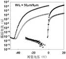
图1为传统薄膜晶体管器件的电学性能图。FIG. 1 is a graph of the electrical properties of a conventional thin film transistor device.
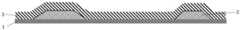
图2为传统薄膜晶体管器件的结构示意图。FIG. 2 is a schematic structural diagram of a conventional thin film transistor device.
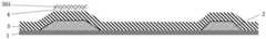
图3为本发明薄膜晶体管器件的结构示意图。FIG. 3 is a schematic structural diagram of the thin film transistor device of the present invention.
图4为本发明制备方法中制备栅极后的器件结构示意图。FIG. 4 is a schematic diagram of the device structure after the gate electrode is prepared in the preparation method of the present invention.
图5为本发明制备方法中制备第一保护层后的器件结构示意图。FIG. 5 is a schematic diagram of the device structure after the first protective layer is prepared in the preparation method of the present invention.
图6为本发明制备方法中制备氧化物半导体层后的器件结构示意图。FIG. 6 is a schematic diagram of the device structure after the oxide semiconductor layer is prepared in the preparation method of the present invention.
图7为本发明制备方法中对铝金属层和钼金属层图案化处理后的器件结构示意图。FIG. 7 is a schematic diagram of the device structure after patterning the aluminum metal layer and the molybdenum metal layer in the preparation method of the present invention.
图8为本发明制备方法中制备阳极图案层后的器件结构示意图。FIG. 8 is a schematic diagram of the device structure after the anode pattern layer is prepared in the preparation method of the present invention.
图9为本发明制备方法中对钛金属层图案化后的器件结构示意图。FIG. 9 is a schematic diagram of the device structure after patterning the titanium metal layer in the preparation method of the present invention.
图10为本发明制备方法中制备第二保护层后的器件结构示意图。FIG. 10 is a schematic diagram of the device structure after preparing the second protective layer in the preparation method of the present invention.
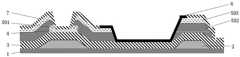
图11为本发明制备方法中制备有机材料层后的器件结构示意图。FIG. 11 is a schematic diagram of the device structure after the organic material layer is prepared in the preparation method of the present invention.
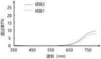
图12为本发明所述掺杂有色染剂的亚克力系光阻材料紫外光谱图。FIG. 12 is an ultraviolet spectrum diagram of the acrylic photoresist material doped with a colorant according to the present invention.
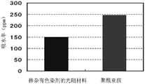
图13为本发明掺杂有色染剂的非亚克力系正型光阻材料与聚酰亚胺的吸水性对比图。FIG. 13 is a comparison diagram of water absorption between the non-acrylic positive photoresist material doped with colorant and polyimide according to the present invention.
附图标记说明:Description of reference numbers:
1:衬底,2:栅极,3:第一保护层,4:氧化物半导体层,5:源、漏极,501:钛金属层,502:铝金属层,503:钼金属层,6:阳极图案层,7:第二保护层,8:有机材料层。1: substrate, 2: gate, 3: first protective layer, 4: oxide semiconductor layer, 5: source and drain, 501: titanium metal layer, 502: aluminum metal layer, 503: molybdenum metal layer, 6 : anode pattern layer, 7: second protective layer, 8: organic material layer.
具体实施方式Detailed ways
本发明提供薄膜晶体管器件,为使本发明的目的、技术方案及效果更加清楚、明确,以下对本发明进一步详细说明。应当理解,此处所描述的具体实施例仅仅用以解释本发明,并不用于限定本发明。The present invention provides a thin film transistor device. In order to make the object, technical solution and effect of the present invention clearer and clearer, the present invention will be described in further detail below. It should be understood that the specific embodiments described herein are only used to explain the present invention, but not to limit the present invention.
液晶显示器上的每一液晶像素点都是由集成在其后的薄膜晶体管来驱动,从而可以做到高速度、高亮度、高对比度显示屏幕信息,TFT-LCD(薄膜晶体管液晶显示器)是多数液晶显示器的一种。TFT器件式屏幕也普遍应用于中高端彩屏手机中,分65536色、16万色,1600万色三种,其显示效果非常出色。但是,如图1所示,利用传统方法以氧化铟镓锌作为氧化物半导层材料制备的TFT在工作过程中受到波长小于470nm的光照后易激发氧化物沟道里氧空位等缺陷态,从而使阈值电压负移。Each liquid crystal pixel on the liquid crystal display is driven by a thin film transistor integrated behind it, so that it can display screen information at high speed, high brightness and high contrast. TFT-LCD (thin film transistor liquid crystal display) is the most A type of display. TFT device-type screens are also widely used in mid-to-high-end color-screen mobile phones, with 65,536 colors, 160,000 colors, and 16 million colors. The display effect is very good. However, as shown in Fig. 1, the TFT prepared by using the traditional method of indium gallium zinc oxide as the oxide semiconductor layer material is easily excited by the light of the wavelength less than 470nm during the working process, such as oxygen vacancies and other defect states in the oxide channel. Negatively shift the threshold voltage.
薄膜晶体管器件可以采用刻蚀阻挡层(Etch Stopper,ES)结构和如图2所示的背沟道刻蚀(Back Channel Etching,BCE)结构。其中,ES器件具有串联电阻小、背沟道无损伤、开启电流大、关态电流低等优点;BCE结构具有工艺简单和所用光罩少的优点。两种结构在器件性能满足需求的前提下,BCE结构使用更为普遍。The thin film transistor device may adopt an etch stopper (Etch Stopper, ES) structure and a back channel etching (BCE) structure as shown in FIG. 2 . Among them, the ES device has the advantages of small series resistance, no damage to the back channel, large turn-on current, and low off-state current; the BCE structure has the advantages of simple process and fewer masks. Under the premise that the device performance meets the requirements of the two structures, the BCE structure is more commonly used.
如图3所示,本发明提供一种薄膜晶体管器件,其中,包括:As shown in FIG. 3, the present invention provides a thin film transistor device, including:
衬底1;
栅极2,形成于所述衬底1上;
第一保护层3,形成于所述衬底1上、并覆盖所述栅极2;A first
氧化物半导体层4,形成于所述第一保护层3上、并与所述栅极2对应设置;The
源、漏极5,形成于所述氧化物半导体层4上;source and drain 5 are formed on the
阳极图案层6,形成于所述漏极上;An
第二保护层7,形成于未被所述阳极图案层6所覆盖的所述源、漏极上;A second
有机材料层8,形成于所述第二保护层7上;其中,所述有机材料层8于所述衬底上的投影覆盖所述氧化物半导体层,且所述有机材料层8被配置为阻挡由该有机材料层8一侧射入的波长小于470纳米的光线。The
在本发明所述薄膜晶体管器件中,所述有机材料层8一侧可以是指有机材料层8远离所述氧化物半导体层4的一侧。本发明中波长小于470纳米的光线通常来说是UV光(紫外光)和短波长可见光(能量较高的可见光)。In the thin film transistor device of the present invention, the side of the
本发明所述有机材料层8被配置为阻挡由该有机材料层8一侧射入的波长小于470纳米的光线,防止所述薄膜晶体管器件中的氧化物半导体层4因受到波长小于470纳米的光线照射在沟道中生成较多的氧空位缺陷。The
本发明所述有机材料层8可以用作所述薄膜晶体管器件的像素定义层或平坦层,也可以单纯作为用于阻挡波长小于470纳米的光线的功能层。The
在本发明的一个实现方式中,所述薄膜晶体管器件包括:由下至上依次层叠设置的衬底1,栅极2,第一保护层(绝缘层)3,氧化物半导体层(有源层)4,源、漏极5,阳极图案层6,第二保护层(金属保护层)7,有机材料层8。In an implementation manner of the present invention, the thin film transistor device includes: a
所述薄膜晶体管器件中源、漏极5由源极和漏极组成;所述源极和漏极之间的位置对应氧化物半导体层4的沟道区域。In the thin film transistor device, the source and the
此外,所述薄膜晶体管器件中还可以包括具有如下层叠结构的区域:所述第二保护层7层叠在所述源、漏极5上,在所述沟道区域所述第二保护层7层叠在所述氧化物半导体层4上。In addition, the thin film transistor device may further include a region having the following stacked structure: the second
在一实施例中,所述薄膜晶体管器件还具有如下区域:所述第一保护层3未层叠所述氧化物半导体层4的区域。在所述第一保护层3上未层叠所述氧化物半导体层4的区域可以设置源、漏极5,即形成了所述薄膜晶体管器件中的电容结构(CST)。In one embodiment, the thin film transistor device further has the following region: the region where the first
在一实施例中,所述薄膜晶体管器件中还具有如下区域:所述第一保护层3与所述第二保护层7接触的区域。由于所述薄膜晶体管器件中所述第一保护层3上存在未层叠设置的氧化物半导体层4和源、漏极5,形成所述第一保护层3与所述第二保护层7接触的区域。In one embodiment, the thin film transistor device further includes the following region: a region where the first
在一实施例中,所述薄膜晶体管器件中还具有如下区域:第二保护层7的断开区域,所述阳极层图案层通过所述断开区域层叠在所述源、漏极上,其中,所述断开区域是为了使沉积的阳极能够和源、漏极接触,从而实现导电。In one embodiment, the thin film transistor device further has the following regions: a disconnection region of the second
在本发明的一个实现方式中,所述栅极(Gate层)2的材料为金属导电材料。所述栅极2的主要材料为低电导率的导电材料制成,具体地,所述金属导电材料为铜、铝、钼、钛中的一种。In an implementation manner of the present invention, the material of the gate electrode (Gate layer) 2 is a metal conductive material. The main material of the
在本发明的一个实现方式中,所述第一保护层3和所述第二保护层7的材料均为SiOx,其中0<x≤2。所述第一保护层3和所述第二保护层7可以是完全相同的SiOx,也可以是不同的SiOx,即所述第一保护层3和所述第二保护层7的SiOx中的x可以相同也可以不同。进一步地,SiOx中1.65≤x≤1.75,可选地,x可以为1.70。In an implementation manner of the present invention, the materials of the first
铟镓锌氧化物(IGZO)是由In2O3、Ga2O3、ZnO通过射频磁控溅射而成的透明非晶氧化物半导体材料。IGZO是一种以ZnO为主体架构同时掺杂Ga、In等重金属元素的混合型半导体(禁带宽度在3.5V),IGZO材料的原子个数比一般为In:Ga:Zn=1:1:1,IGZO因独特的电子结构,使其具有许多优异的性能,如IGZO的电子迁移率可以达到10cm2V-1s-1以上,而非晶硅的往往小于1cm2V-1s-1。IGZO还具有可见光区高透过率的优点,可以用来制备透明的显示器件及柔性电路。IGZO的制备温度低,因此生产成本较低,以IGZO制备的TFT器件具有较高的开关比以及较少的亚阈值摆幅。在本发明的一个实现方式中,氧化物半导体层4的材料为铟镓锌氧化物。当然,本发明所述氧化物半导体层4的材料并不限于铟镓锌氧化物,还可以其他金属氧化物,例如稀土金属氧化物。Indium Gallium Zinc Oxide (IGZO) is a transparent amorphous oxide semiconductor material made of In2 O3 , Ga2 O3 and ZnO by radio frequency magnetron sputtering. IGZO is a hybrid semiconductor with ZnO as the main structure and doped with heavy metal elements such as Ga and In (the band gap is 3.5V). The atomic ratio of IGZO materials is generally In:Ga:Zn=1:1: 1. IGZO has many excellent properties due to its unique electronic structure. For example, the electron mobility of IGZO can reach more than 10cm2 V-1 s-1 , while that of amorphous silicon is often less than 1cm2 V-1 s-1 . IGZO also has the advantage of high transmittance in the visible region, and can be used to prepare transparent display devices and flexible circuits. The preparation temperature of IGZO is low, so the production cost is low, and the TFT device prepared with IGZO has a higher switching ratio and less sub-threshold swing. In an implementation manner of the present invention, the material of the
在本发明的一个实现方式中,所述源、漏极(SD层)5均包括依次层叠设置的钛金属层(Ti层)501、铝金属层(Al层)502和钼金属层(Mo层)503。具体地,所述源、漏极5为依次层叠设置的Ti层501、Al层502、Mo层503。也就是说,由Ti层501、Al层502、Mo层503依次层叠后设置在所述氧化物半导体层4上。Al层502作为导电层,Ti层501和Mo层503是作为功能层,其中,在制备过程中所述Ti层501能够对所述氧化物半导体层4的起到刻蚀保护作用;而且与Al相比,Ti和Mo的阻抗比较高。基于此,所述源、漏极5中,所述Al层502的厚度可以大于Ti层501的厚度和Mo层503的厚度,即所述Al层502的厚度最大。In an implementation of the present invention, the source and drain electrodes (SD layers) 5 each include a titanium metal layer (Ti layer) 501, an aluminum metal layer (Al layer) 502 and a molybdenum metal layer (Mo layer) that are stacked in sequence. ) 503. Specifically, the source and
在本发明的一个实现方式中,所述阳极图案层6的材料为ITO材料。ITO(IndiumTin Oxides)是一种N型氧化物半导体-氧化铟锡,ITO薄膜层即铟锡氧化物半导体透明导电层。In an implementation of the present invention, the material of the
在本发明的一个实施方式中,所述有机材料层8为有色的有机材料层8或黑色的有机材料层8。本发明所述有色的有机材料层8或黑色的有机材料层8能够对波长小于470纳米的光线进行吸收或反射,从而达到有效阻挡该有机材料层8一侧射入的波长小于470纳米的光线的效果,防止所述薄膜晶体管器件中的IGZO因受到光照在沟道中生成较多的氧空位缺陷。In an embodiment of the present invention, the
本发明中所述有机材料层8可以通过采用有色的有机材料来达到阻挡波长小于470纳米的光线的目的。具体地,本发明所述有色的有机材料可以是自带颜色的有机材料(有机材料本身即是有色的);所述有色的有机材料也可以通过掺杂其他有色的物质得到的有色的有机材料。其中,所述有色是指非无色透明的颜色。The
在其中一个实施例中,所述有机材料层8包括掺杂有黑色高分子或有色染剂的有机材料。具体来说,本发明所述黑色高分子至少包括能够完全吸收光线或仅反射波长小于390nm的非可见光的高分子材料;所述有色染剂至少包括能反射波长小于470nm的可见光的染剂。本发明所述有机材料层8包括掺杂有一种或多种黑色高分子或有色染剂的有机材料,对波长小于470纳米的光线进行吸收或反射,进而实现阻挡由该有机材料层8一侧射入的波长小于470纳米的光线。In one embodiment, the
在本发明的一个实现方式中,所述有色的有机材料为掺杂有色染剂的有机材料。本发明通过在有机材料中掺杂有色染剂使无色透明的有机材料转为有色的有机材料或改变原先的有机材料的颜色。可见,掺杂有色染剂的有机材料通过改变有色染剂的种类以及用量能够很方便地改变获得所需要的颜色的有机材料,能够实现阻挡特定波长范围的光线。In an implementation of the present invention, the colored organic material is an organic material doped with a colorant. The present invention converts colorless and transparent organic materials into colored organic materials or changes the color of the original organic materials by doping organic materials with colorants. It can be seen that the organic material doped with a colorant can easily change the organic material to obtain the desired color by changing the type and amount of the colorant, and can block light in a specific wavelength range.
在本发明的一个实现方式中,本发明通过在有机材料中掺杂黑色有机类染料获取黑色的有机材料。黑色有机材料可以阻隔包括波长小于470纳米的光线在内的几乎所有波长的光,实现对器件的氧化物半导体层3保护,提高器件的稳定性。In an implementation manner of the present invention, the present invention obtains black organic materials by doping organic materials with black organic dyes. The black organic material can block light of almost all wavelengths including light with a wavelength of less than 470 nanometers, realize protection of the
在本发明的一个实现方式中,所述黑色有机类染料包括二萘嵌苯、聚氨酯基黑色高分子中的一种或两种。所述二萘嵌苯对光线具有良好的阻隔效果,且化学性质较为稳定。In an implementation of the present invention, the black organic dye includes one or both of perylene and polyurethane-based black polymers. The perylene has good blocking effect on light and relatively stable chemical properties.
在本发明的一个实现方式中,所述有色染剂为酞菁类染料、吡咯并吡咯二酮类有机染料中的一种或多种。试验表明,与其他有机染料相比,本发明酞菁类染料、吡咯并吡咯二酮类有机染料能够有效阻挡紫外光以及大部分可见光。In an implementation of the present invention, the colored dye is one or more of phthalocyanine dyes and diketopyrrolopyrrole organic dyes. Experiments show that, compared with other organic dyes, the phthalocyanine dyes and diketopyrrolopyrrole organic dyes of the present invention can effectively block ultraviolet light and most visible light.
在本发明的一个实现方式中,所述有色的有机材料为非黑色的有色有机材料,具体可以通过在有机材料中掺杂上述的有色染剂制备得到。所述非黑色的有色有机材料仅能透过能量较低的红外光,即非黑色的有色有机材料可以阻隔短波长光和大部分可见光。换句话说,所述非黑色的有色有机材料可以透过波长大于或等于470纳米中的光线,阻挡波长小于470纳米的光线。与阻挡几乎所有光线的黑色有机材料相比,可见,所述非黑色的有色有机材料在实现对器件保护的同时也可以实现红外光对位的功能,更易于实现有机材料图案化。In an implementation manner of the present invention, the colored organic material is a non-black colored organic material, which can be specifically prepared by doping the above-mentioned colored dye into the organic material. The non-black colored organic material can only transmit infrared light with lower energy, that is, the non-black colored organic material can block short-wavelength light and most visible light. In other words, the non-black colored organic material can transmit light with wavelengths greater than or equal to 470 nanometers, and block light with wavelengths less than 470 nanometers. Compared with the black organic material that blocks almost all light, it can be seen that the non-black colored organic material can realize the function of infrared light alignment while realizing the protection of the device, and it is easier to realize the patterning of the organic material.
在本发明的一个实施方式中,所述有机材料为光阻材料。换句话说,所述有机材料层的材料可以选择掺杂有黑色高分子或有色染剂的光阻材料。所述光阻材料的主要成份可以为聚亚酰胺和丙烯酸酯单体的组合物或包括甲酚醛树脂和丙烯酸酯单体的组合物,所述光阻材料也可以市售光阻材料。进一步地,所述光阻材料为亚克力系负型光阻材料或非亚克力系正型光阻材料。In one embodiment of the present invention, the organic material is a photoresist material. In other words, the material of the organic material layer can be selected from a photoresist material doped with a black polymer or a colorant. The main components of the photoresist material may be a composition of polyimide and acrylate monomers or a composition comprising cresol novolac resin and acrylate monomers, and the photoresist material may also be commercially available photoresist materials. Further, the photoresist material is an acrylic type negative type photoresist material or a non-acrylic type positive type photoresist material.
在本发明的一个实施方式中,所述有机材料层8的材料可以为掺杂有色染剂的亚克力系负型光阻材料。如图12所示,利用不同波长光对掺杂有色染剂的亚克力系负型光阻材料(具体为掺杂吡咯并吡咯二酮的亚克力系负型光阻材料,其中吡咯并吡咯二酮的掺杂量为70%)进行两次照射实验(试验1和试验2)发现,掺杂有色染剂的亚克力系负型光阻材料对波长小于650纳米的光线具有良好的阻挡效果,特别是几乎能够完全阻挡波长小于550纳米的光,而对于波长大于650nm的光则具有一定的透过性。可见,所述掺杂有色染剂的亚克力系负型光阻材料可过滤掉大部分UV光。同时,长波的光(如红外光)可穿透所述掺杂有色染剂的亚克力系负型光阻材料,因此,在制备过程中可利用红外光进行定位。In one embodiment of the present invention, the material of the
此外,如图13所示,掺杂有色染剂的非亚克力系正型光阻材料(具体为掺杂吡咯并吡咯二酮的亚克力系正型光阻材料,其中吡咯并吡咯二酮的掺杂量为70%)具有比聚酰亚胺还低的吸水性,有利于提高薄膜晶体管器件性能。In addition, as shown in FIG. 13 , non-acrylic positive photoresist materials doped with colorants (specifically, acrylic positive photoresist materials doped with diketopyrrolopyrrole, wherein the doping of diketopyrrolopyrrole) 70%) has lower water absorption than polyimide, which is beneficial to improve the performance of thin film transistor devices.
在本发明的一个实施方式中,所述光阻材料中所述黑色高分子或有色染剂的掺杂量约为60%-100%时,可以有效实现遮光效果,避免氧化物半导体层产生氧空位缺陷。本发明所述光阻材料中所述黑色高分子或有色染剂的掺杂量根据实际的遮光效果的需要进行设定。可选地,所述光阻材料中所述黑色高分子或有色染剂的掺杂量为60%-99%,又如70%、80%、90%。In an embodiment of the present invention, when the doping amount of the black polymer or colored dye in the photoresist material is about 60%-100%, the light-shielding effect can be effectively achieved and the generation of oxygen in the oxide semiconductor layer can be avoided. vacancy defect. The doping amount of the black polymer or the colored dye in the photoresist material of the present invention is set according to the needs of the actual light-shielding effect. Optionally, the doping amount of the black polymer or colored dye in the photoresist material is 60%-99%, for example, 70%, 80%, and 90%.
需要说明的是,本发明所述的染料是指带有颜色的化学物质,能够使掺杂带有颜色的化学物质后的有机材料实现阻隔波长小于470纳米的光线的化学物质,并不限于传统的化学染料。It should be noted that the dye mentioned in the present invention refers to a chemical substance with a color, which can make the organic material doped with a chemical substance with a color realize the blocking of light with a wavelength of less than 470 nanometers, and is not limited to traditional chemical substances. chemical dyes.
本发明所述有机材料层8的厚度会影响透光性,在本发明的一个实施方式中,所述有机材料层8的厚度为1~3μm。对于所述有机材料层8的材料为掺杂有色染剂的有机材料来说,所述有机材料层8的厚度为1~3μm,能同时实现对氧化物半导体形成遮光效果避免产生氧空位缺陷,同时也能保证红外光的透过上述厚度的所述有机材料层8,实现制备过程中通过所述红外光进行定位。The thickness of the
本发明可以根据氧化物半导体层4所采用的氧化物配置相应的有机材料层8阻挡光线的波长范围。具体地,基于所述氧化物对不同波长光线产生的氧空位缺陷敏感程度不同,配置相应的有机材料层8针对性地阻挡使所述氧化物易产生氧空位缺陷对应波长范围的光线。在本发明的一个实现方式中,所述有机材料层8阻挡的光线波长介于300纳米至470纳米之间。In the present invention, the corresponding
本发明还提供一种铟镓锌薄膜晶体管器件的制备方法,其中,包括:The present invention also provides a method for preparing an indium gallium zinc thin film transistor device, which includes:
S101、提供一衬底1;S101, providing a
S102、在所述衬底1上沉积第一金属层,并对所述第一金属层进行图案化处理,形成栅极2;S102, depositing a first metal layer on the
S103、在所述衬底1和栅极2上沉积第一保护层3,其中所述第一保护层覆盖所述栅极;S103, depositing a first
S104、在所述第一保护层3上依次沉积氧化物和第二金属层,并对所述第二金属层进行图案化处理形成第一次图案化处理后的第二金属层,再对所述氧化物进行图案化处理形成氧化物半导体层4;S104 , depositing an oxide and a second metal layer on the first
S105、在所述第一次图案化处理后的第二金属层上沉积第三金属层,并对所述第三金属层图案化处理,形成图案化处理后的第三金属层;S105, depositing a third metal layer on the second metal layer after the first patterning process, and patterning the third metal layer to form a patterned third metal layer;
S106、在所述图案化处理后的第三金属层上沉积阳极材料,并对所述阳极材料进行图案化处理,形成阳极图案层6;S106, depositing an anode material on the patterned third metal layer, and patterning the anode material to form an
S107、对所述第一次图案化处理后的第二金属层再次进行图案处理,形成源、漏极5;S107 , patterning the second metal layer after the first patterning process again to form source and
S108、在所述源、漏极5上沉积保护层材料,对保护层材料进行图案化处理,在未被所述阳极图案层6所覆盖的所述源、漏极上形成第二保护层7;S108 , depositing a protective layer material on the source and
S109、在所述第二保护层7上形成有机材料层8,所述有机材料层8于所述衬底上的投影覆盖所述氧化物半导体层,且所述有机材料层8被配置为阻挡由该有机材料层8一侧射入的波长小于470纳米的光线。S109 , forming an
本发明制备得到的所述有机材料层8是被配置为阻挡由该有机材料层8一侧射入的波长小于470纳米的光线,能够防止所述薄膜晶体管器件中的氧化物半导体层9因受到波长小于470纳米的光线照射在沟道中生成较多的氧空位缺陷,进而能有效防止阈值电压负移,进一步提高器件的稳定性。The
更具体地,所述制备铟镓锌氧化物TFT基板包括:More specifically, the preparation of the indium gallium zinc oxide TFT substrate includes:
S101、提供一衬底1;S101, providing a
S102、在所述衬底1上沉积第一金属层,并对所述第一金属层进行图案化处理,形成栅极21(Gate层),如图4所示;S102, depositing a first metal layer on the
S103、在所述栅极2上沉积SiOx材料,制备得到第一保护层3,如图5所示,其中,0<x≤2;S103 , depositing SiOx material on the
S104、在所述第一保护层3上沉积铟镓锌氧化物、Ti层,并对所述Ti层进行图案化处理形成第一次图案化处理后的Ti层501,在对所述铟镓锌氧化物进行图案化处理,形成与所述栅极2对应的氧化物半导体层4,如图6所示;S104 , depositing an indium gallium zinc oxide and a Ti layer on the first
S105、在所述第一次图案化处理后的Ti层501上连续沉积Al层502、Mo层503,经过涂胶、曝光、显影、对Al层502、Mo层503刻蚀后制备得到图案化处理后的Al层502、Mo层503,如图7所示;S105 , continuously depositing an
S106、在所述图案化处理后的Al层502、Mo层503上沉积ITO材料,经过涂胶、曝光、显影、刻蚀后,制备得到形成阳极图案层6,如图8所示;S106, depositing an ITO material on the patterned
S107、对所述第一次图案化处理后的Ti层501再次进行图案处理,以漏出所述氧化物半导体层上方的通道,得到第二次图案化处理后的Ti层,即形成由第二次图案化处理后的Ti层501、图案化处理后的Al层502、Mo层503组成的源、漏极5,如图9所示。S107 , patterning the
S108、在所述源、漏极5上沉积SiOx材料,对SiOx材料进行图案化处理,在未被所述阳极图案层6所覆盖的所述源、漏极5上形成第二保护层7,如图10所示,其中,0<x≤2;S108 , depositing SiOx material on the source and
S109、在所述阳极图案层6上沉积掺杂有色染剂或黑色高分子的光阻材料形成有机材料层8,所述有机材料层8于所述衬底1上的投影覆盖所述氧化物半导体层4,如图11所示。S109, depositing a photoresist material doped with a colorant or black polymer on the
所述S101具体是,在衬底1上通过沉积金属导电材料,依次经过涂胶、曝光、显影、刻蚀工艺形成栅极2(Gate层),栅极2的主要材料为低电导率的导电材料制成,如铜(Cu)、铝(Al)、钼(Mo)、钛(Ti)等。其中,图案化处理的涂胶、曝光、显影、刻蚀工艺是本领域中的成熟工艺,因此不再赘述。The S101 is specifically, by depositing a metal conductive material on the
所述S104至S107中,所述第二金属层为Ti层501,所述第三金属层为Al层502、Mo层503。其中,在第一保护层上连续沉降IGZO/Ti,然后通过涂胶/曝光/显影、刻蚀工艺对Ti层及IGZO进行图案化。可选地,工艺过程中Ti层利用刻蚀液BCl3/Cl2进行刻蚀,而IGZO通过磷酸进行刻蚀形成,Al层502、Mo层503通过铝酸进行刻蚀,而磷酸和铝酸均无法对Ti层进行刻蚀。因此,本发明中所述Ti层可以在刻蚀所述Al层502、Mo层503以及阳极材料过程中对所述氧化物半导体层4进行保护,避免在上述过程中对氧化物半导体层4造成损伤或污染。In S104 to S107 , the second metal layer is the
在本发明的一个实现方式中,所述有机材料层8的形成工艺包括磁控溅射、化学气相沉积、原子沉积、旋涂、喷墨打印工艺中任意一种。In an implementation manner of the present invention, the formation process of the
下面通过具体的实施例对本发明的技术方案进行说明。The technical solutions of the present invention will be described below through specific embodiments.
制备一种铟镓锌薄膜晶体管器件,包括如下步骤:The preparation of an indium gallium zinc thin film transistor device includes the following steps:
步骤1、在衬底1上通过沉积金属Cu,依次经过涂胶、曝光、显影、刻蚀工艺形成栅极2,如图4所示;
步骤2、在所述栅极2上沉积SiO1.7材料,制备得到第一保护层3,如图5所示;
步骤3、在所述第一保护层3上连续沉积铟镓锌氧化物和金属Ti层501,依次进行涂胶、曝光、显影后,先使用刻蚀液BCl3/Cl2刻蚀表面的Ti层501得到第一次图案化处理后的Ti层501,再使用过磷酸刻蚀液刻蚀铟镓锌氧化物,形成与所述栅极对应的氧化物半导体层4,如图6所示;
步骤4、在所述第一次图案化处理后的Ti层501上连续沉积Al层502、Mo层503(Al/Mo),经过涂胶、曝光、显影后,采用刻蚀液铝酸对Al层502和Mo层503进行刻蚀,得到图案化处理后的Al层502、Mo层503,如图7所示;
步骤5、在所述图案化处理后的Al层502、Mo层503上沉积ITO材料,经过涂胶、曝光、显影、刻蚀后,制备得到阳极图案层6如图8所示;
步骤6、对所述第一次图案化处理后的Ti层501再次使用刻蚀液BCl3/Cl2进行刻蚀,以漏出所述氧化物半导体层上方的通道,形成第二次图案化处理后的Ti层501,即形成由第二次图案化处理后的Ti层501、图案化处理后的Al层502、Mo层503组成的源、漏极5,如图9所示;
步骤7、在所述源、漏极5上沉积SiO1.7材料,对SiO1.7材料进行图案化处理,在未被所述阳极图案层6所覆盖的所述源、漏极5上形成第二保护层7,如图10所示;
步骤8、在所述阳极图案层6上采用旋涂工艺沉积掺杂吡咯并吡咯二酮的亚克力系负型光阻材料,其中所述吡咯并吡咯二酮的掺杂量为70%,形成有机材料层8(PDL)图案,并对所述有机材料层8采用湿法刻蚀工艺进行图案化处理,其中所述有机材料层8于所述衬底1上的投影覆盖所述氧化物半导体层4,如图11所示。
应当理解的是,本发明的应用不限于上述的举例,对本领域普通技术人员来说,可以根据上述说明加以改进或变换,所有这些改进和变换都应属于本发明所附权利要求的保护范围。It should be understood that the application of the present invention is not limited to the above examples. For those of ordinary skill in the art, improvements or transformations can be made according to the above descriptions, and all these improvements and transformations should belong to the protection scope of the appended claims of the present invention.
Claims (8)
Priority Applications (1)
| Application Number | Priority Date | Filing Date | Title |
|---|---|---|---|
| CN202010559986.1ACN113451414B (en) | 2020-06-18 | 2020-06-18 | Thin film transistor device and preparation method thereof |
Applications Claiming Priority (1)
| Application Number | Priority Date | Filing Date | Title |
|---|---|---|---|
| CN202010559986.1ACN113451414B (en) | 2020-06-18 | 2020-06-18 | Thin film transistor device and preparation method thereof |
Publications (2)
| Publication Number | Publication Date |
|---|---|
| CN113451414A CN113451414A (en) | 2021-09-28 |
| CN113451414Btrue CN113451414B (en) | 2022-07-29 |
Family
ID=77808317
Family Applications (1)
| Application Number | Title | Priority Date | Filing Date |
|---|---|---|---|
| CN202010559986.1AActiveCN113451414B (en) | 2020-06-18 | 2020-06-18 | Thin film transistor device and preparation method thereof |
Country Status (1)
| Country | Link |
|---|---|
| CN (1) | CN113451414B (en) |
Citations (1)
| Publication number | Priority date | Publication date | Assignee | Title |
|---|---|---|---|---|
| KR20200067361A (en)* | 2018-12-04 | 2020-06-12 | 엘지디스플레이 주식회사 | Thin film trnasistors and display device comprising the same |
Family Cites Families (19)
| Publication number | Priority date | Publication date | Assignee | Title |
|---|---|---|---|---|
| US8309419B2 (en)* | 2009-02-04 | 2012-11-13 | Freescale Semiconductor, Inc. | CMOS integration with metal gate and doped high-K oxides |
| TWI511288B (en)* | 2009-03-27 | 2015-12-01 | Semiconductor Energy Lab | Semiconductor device |
| CN101894760B (en)* | 2010-06-10 | 2012-06-20 | 友达光电股份有限公司 | Thin film transistor and manufacturing method thereof |
| US9054204B2 (en)* | 2012-01-20 | 2015-06-09 | Sony Corporation | Thin-film transistor, method of manufacturing the same, display unit, and electronic apparatus |
| KR20130111872A (en)* | 2012-04-02 | 2013-10-11 | 삼성디스플레이 주식회사 | Thin film transistor, thin film transistor array panel including the same and manufacturing method thereof |
| US8981374B2 (en)* | 2013-01-30 | 2015-03-17 | Semiconductor Energy Laboratory Co., Ltd. | Semiconductor device |
| CN104425542B (en)* | 2013-08-26 | 2017-08-04 | 昆山工研院新型平板显示技术中心有限公司 | A kind of organic light-emitting display device and preparation method thereof |
| KR20150033155A (en)* | 2013-09-23 | 2015-04-01 | 삼성디스플레이 주식회사 | Thin film transistor and method of the same |
| CN104513370A (en)* | 2013-09-26 | 2015-04-15 | 海洋王照明科技股份有限公司 | Diketopyrrolo pyrrole based copolymer, preparation method, and applications thereof |
| CN103762247B (en)* | 2014-01-10 | 2016-07-06 | 北京京东方光电科技有限公司 | Thin film transistor (TFT), array base palte and preparation method thereof and organic electroluminescence display panel |
| CN104157701B (en)* | 2014-09-02 | 2017-09-01 | 深圳市华星光电技术有限公司 | Manufacturing method and structure of oxide semiconductor TFT substrate |
| WO2016084778A1 (en)* | 2014-11-28 | 2016-06-02 | シャープ株式会社 | Liquid crystal display device |
| CN105949425B (en)* | 2016-06-07 | 2019-01-15 | 安徽建筑大学 | Polyurethane-based black high-molecular dye, preparation method and application |
| CN106547168B (en)* | 2016-10-28 | 2020-09-01 | 深圳市华星光电技术有限公司 | Black matrix material composition and application |
| CN108987482B (en)* | 2017-05-31 | 2022-05-17 | 乐金显示有限公司 | Thin film transistor, gate driver including the same, and display device including the gate driver |
| CN109254340B (en)* | 2017-07-12 | 2021-08-10 | 张家港康得新光电材料有限公司 | Infrared and ultraviolet cut-off composition, infrared and ultraviolet cut-off film and application of infrared and ultraviolet cut-off film |
| WO2021097733A1 (en)* | 2019-11-21 | 2021-05-27 | 重庆康佳光电技术研究院有限公司 | Thin film transistor and manufacturing method therefor, and thin film transistor array |
| CN111048593A (en)* | 2019-11-25 | 2020-04-21 | 南京中电熊猫液晶显示科技有限公司 | A kind of thin film transistor and its manufacturing method |
| CN110998857A (en)* | 2019-11-27 | 2020-04-10 | 重庆康佳光电技术研究院有限公司 | A kind of thin film transistor and its preparation method and thin film transistor array |
- 2020
- 2020-06-18CNCN202010559986.1Apatent/CN113451414B/enactiveActive
Patent Citations (1)
| Publication number | Priority date | Publication date | Assignee | Title |
|---|---|---|---|---|
| KR20200067361A (en)* | 2018-12-04 | 2020-06-12 | 엘지디스플레이 주식회사 | Thin film trnasistors and display device comprising the same |
Also Published As
| Publication number | Publication date |
|---|---|
| CN113451414A (en) | 2021-09-28 |
Similar Documents
| Publication | Publication Date | Title |
|---|---|---|
| CN105552027B (en) | The production method and array substrate of array substrate | |
| CN105489552B (en) | The production method of LTPS array substrates | |
| CN101359693B (en) | Thin film transistor, array substrate having the transistor, and method of manufacturing the array substrate | |
| KR101533391B1 (en) | Thin film transistor substrate and manufacturing method thereof | |
| CN105446000B (en) | The production method of eyeshield type liquid crystal display device | |
| CN101819362B (en) | TFT-LCD (Thin Film Transistor Liquid Crystal Display) array substrate and manufacture method thereof | |
| WO2016065796A1 (en) | Coa substrate and manufacturing method thereof, and display device | |
| WO2017166341A1 (en) | Method for manufacturing tft substrate and manufactured tft substrate | |
| WO2016165185A1 (en) | Manufacturing method for dual-gate oxide semiconductor tft substrate, and structure of dual-gate oxide semiconductor tft substrate | |
| CN104157696B (en) | Thin film transistor and preparation method thereof, as well as array baseplate and liquid crystal display device | |
| CN105655359A (en) | Method for manufacturing TFT (thin-film transistor) substrates | |
| CN105652541A (en) | Manufacturing method of array substrate and liquid crystal display panel | |
| CN104900712A (en) | TFT substrate structure manufacturing method and TFT substrate structure thereof | |
| CN110808276A (en) | OLED display panel, preparation method thereof and OLED display device | |
| TW201351658A (en) | Thin film transistor substrate, manufacturing method thereof and display | |
| EP3346496B1 (en) | Array substrate and display device | |
| CN109003943B (en) | Array substrate and preparation method thereof | |
| WO2012086595A1 (en) | Semiconductor device, color filter substrate, display device provided with color filter substrate, and method for manufacturing semiconductor device | |
| CN111739841B (en) | In-cell touch panel with top gate structure and manufacturing method | |
| CN113451414B (en) | Thin film transistor device and preparation method thereof | |
| WO2017166337A1 (en) | Thin-film transistor, method for fabricating thin-film transistor, and liquid-crystal display panel | |
| CN103165530B (en) | Thin film transistor (TFT) array substrate and manufacture method and display device thereof | |
| CN113451413B (en) | A kind of thin film transistor device and preparation method thereof | |
| KR101251351B1 (en) | Thin film transistor substrate, method for making the substrate and display panel having the substrate | |
| KR20120072817A (en) | Liquid crystal display device |
Legal Events
| Date | Code | Title | Description |
|---|---|---|---|
| PB01 | Publication | ||
| PB01 | Publication | ||
| SE01 | Entry into force of request for substantive examination | ||
| SE01 | Entry into force of request for substantive examination | ||
| GR01 | Patent grant | ||
| GR01 | Patent grant | ||
| CP03 | Change of name, title or address | Address after:402760 No.69, Wushan Road, Biquan street, Bishan District, Chongqing Patentee after:Chongqing Kangjia Optoelectronic Technology Co.,Ltd. Country or region after:China Address before:402760 No.69, Wushan Road, Biquan street, Bishan District, Chongqing Patentee before:Chongqing Kangjia Photoelectric Technology Research Institute Co.,Ltd. Country or region before:China | |
| CP03 | Change of name, title or address |