CN113451293B - Electrostatic discharge protection circuit - Google Patents
Electrostatic discharge protection circuitDownload PDFInfo
- Publication number
- CN113451293B CN113451293BCN202010224088.0ACN202010224088ACN113451293BCN 113451293 BCN113451293 BCN 113451293BCN 202010224088 ACN202010224088 ACN 202010224088ACN 113451293 BCN113451293 BCN 113451293B
- Authority
- CN
- China
- Prior art keywords
- inverter
- terminal
- voltage
- transistor
- nmos transistor
- Prior art date
- Legal status (The legal status is an assumption and is not a legal conclusion. Google has not performed a legal analysis and makes no representation as to the accuracy of the status listed.)
- Active
Links
Images

Classifications
- H—ELECTRICITY
- H10—SEMICONDUCTOR DEVICES; ELECTRIC SOLID-STATE DEVICES NOT OTHERWISE PROVIDED FOR
- H10D—INORGANIC ELECTRIC SEMICONDUCTOR DEVICES
- H10D89/00—Aspects of integrated devices not covered by groups H10D84/00 - H10D88/00
- H10D89/60—Integrated devices comprising arrangements for electrical or thermal protection, e.g. protection circuits against electrostatic discharge [ESD]
- H10D89/601—Integrated devices comprising arrangements for electrical or thermal protection, e.g. protection circuits against electrostatic discharge [ESD] for devices having insulated gate electrodes, e.g. for IGFETs or IGBTs
- H10D89/811—Integrated devices comprising arrangements for electrical or thermal protection, e.g. protection circuits against electrostatic discharge [ESD] for devices having insulated gate electrodes, e.g. for IGFETs or IGBTs using FETs as protective elements
- H—ELECTRICITY
- H02—GENERATION; CONVERSION OR DISTRIBUTION OF ELECTRIC POWER
- H02H—EMERGENCY PROTECTIVE CIRCUIT ARRANGEMENTS
- H02H3/00—Emergency protective circuit arrangements for automatic disconnection directly responsive to an undesired change from normal electric working condition with or without subsequent reconnection ; integrated protection
- H02H3/02—Details
- H02H3/04—Details with warning or supervision in addition to disconnection, e.g. for indicating that protective apparatus has functioned
- H02H3/046—Signalling the blowing of a fuse
- H—ELECTRICITY
- H02—GENERATION; CONVERSION OR DISTRIBUTION OF ELECTRIC POWER
- H02H—EMERGENCY PROTECTIVE CIRCUIT ARRANGEMENTS
- H02H9/00—Emergency protective circuit arrangements for limiting excess current or voltage without disconnection
- H02H9/04—Emergency protective circuit arrangements for limiting excess current or voltage without disconnection responsive to excess voltage
- H02H9/045—Emergency protective circuit arrangements for limiting excess current or voltage without disconnection responsive to excess voltage adapted to a particular application and not provided for elsewhere
- H—ELECTRICITY
- H03—ELECTRONIC CIRCUITRY
- H03K—PULSE TECHNIQUE
- H03K17/00—Electronic switching or gating, i.e. not by contact-making and –breaking
- H03K17/08—Modifications for protecting switching circuit against overcurrent or overvoltage
- H03K17/081—Modifications for protecting switching circuit against overcurrent or overvoltage without feedback from the output circuit to the control circuit
- H03K17/08104—Modifications for protecting switching circuit against overcurrent or overvoltage without feedback from the output circuit to the control circuit in field-effect transistor switches
- H—ELECTRICITY
- H10—SEMICONDUCTOR DEVICES; ELECTRIC SOLID-STATE DEVICES NOT OTHERWISE PROVIDED FOR
- H10D—INORGANIC ELECTRIC SEMICONDUCTOR DEVICES
- H10D89/00—Aspects of integrated devices not covered by groups H10D84/00 - H10D88/00
- H10D89/60—Integrated devices comprising arrangements for electrical or thermal protection, e.g. protection circuits against electrostatic discharge [ESD]
- H10D89/601—Integrated devices comprising arrangements for electrical or thermal protection, e.g. protection circuits against electrostatic discharge [ESD] for devices having insulated gate electrodes, e.g. for IGFETs or IGBTs
- H10D89/811—Integrated devices comprising arrangements for electrical or thermal protection, e.g. protection circuits against electrostatic discharge [ESD] for devices having insulated gate electrodes, e.g. for IGFETs or IGBTs using FETs as protective elements
- H10D89/819—Bias arrangements for gate electrodes of FETs, e.g. RC networks or voltage partitioning circuits
- H—ELECTRICITY
- H10—SEMICONDUCTOR DEVICES; ELECTRIC SOLID-STATE DEVICES NOT OTHERWISE PROVIDED FOR
- H10D—INORGANIC ELECTRIC SEMICONDUCTOR DEVICES
- H10D89/00—Aspects of integrated devices not covered by groups H10D84/00 - H10D88/00
- H10D89/60—Integrated devices comprising arrangements for electrical or thermal protection, e.g. protection circuits against electrostatic discharge [ESD]
- H10D89/601—Integrated devices comprising arrangements for electrical or thermal protection, e.g. protection circuits against electrostatic discharge [ESD] for devices having insulated gate electrodes, e.g. for IGFETs or IGBTs
- H10D89/911—Integrated devices comprising arrangements for electrical or thermal protection, e.g. protection circuits against electrostatic discharge [ESD] for devices having insulated gate electrodes, e.g. for IGFETs or IGBTs using passive elements as protective elements
Landscapes
- Semiconductor Integrated Circuits (AREA)
Abstract
Translated fromChinese
Description
Translated fromChinese技术领域technical field
本申请涉及集成电路技术领域,特别是涉及一种静电放电保护电路。The present application relates to the technical field of integrated circuits, and in particular, to an electrostatic discharge protection circuit.
背景技术Background technique
现在半导体的制程越来越先进,半导体器件越来越小,结深(junction depth)越来越浅,氧化层越来越薄,半导体集成电路的可靠性面临的挑战越来越大,尤其是静电保护变得愈发重要。据统计,有很多半导体产品的失效是有静电损伤引起的。为了更好的保护集成电路不受静电损伤,需要设置静电放电保护电路对集成电路进行保护。Now the semiconductor process is getting more and more advanced, the semiconductor devices are getting smaller and smaller, the junction depth is getting shallower and the oxide layer is getting thinner and thinner, and the reliability of semiconductor integrated circuits is facing increasing challenges, especially Electrostatic protection is becoming more and more important. According to statistics, the failure of many semiconductor products is caused by electrostatic damage. In order to better protect the integrated circuit from electrostatic damage, it is necessary to set an electrostatic discharge protection circuit to protect the integrated circuit.
常规的集成电路产品通常具备静电保护的设计,通常所有的引出焊盘都有对应的静电保护电路,这些保护电路能够保证所有的引出焊盘在遇到静电放电(ElectrostaticDischarge,ESD)时,能够快速泄放ESD静电,从而保护集成电路产品不受ESD损伤。为了保证静电发生的时间内能充分泄放静电电流,现有的静电放电保护电路的电阻和电容会占用比较大的设计空间,即现有的静电放电保护电路为了达到较好的静电保护效果需要较大的RC时间常数,从而使得静电放电保护电路的面积较大;同时,现有的静电保护电路还易受到噪声的影响。Conventional integrated circuit products are usually designed with electrostatic protection. Usually, all lead-out pads have corresponding electrostatic protection circuits. These protection circuits can ensure that all lead-out pads can quickly respond to Electrostatic Discharge (ESD). Discharge ESD static electricity to protect integrated circuit products from ESD damage. In order to ensure that the electrostatic current can be fully discharged within the time of the occurrence of static electricity, the resistance and capacitance of the existing electrostatic discharge protection circuit will occupy a relatively large design space, that is, the existing electrostatic discharge protection circuit needs to achieve a better electrostatic protection effect. The larger RC time constant makes the area of the electrostatic discharge protection circuit larger; at the same time, the existing electrostatic protection circuit is also easily affected by noise.
发明内容SUMMARY OF THE INVENTION
基于此,有必要针对现有技术中存在的静电放电保护电路面积较大,且易受噪声影响的问题提供一种静电放电保护电路。Based on this, it is necessary to provide an electrostatic discharge protection circuit in view of the problems in the prior art that the electrostatic discharge protection circuit has a large area and is easily affected by noise.
为了实现上述目的,一方面,本发明提供了一种静电放电保护电路,包括:In order to achieve the above objects, on the one hand, the present invention provides an electrostatic discharge protection circuit, comprising:
脉冲检测单元,用于检测静电脉冲信号,其第一端连接第一电压,第二端连接第二电压,第三端输出脉冲检测信号;The pulse detection unit is used to detect the electrostatic pulse signal, the first end of which is connected to the first voltage, the second end is connected to the second voltage, and the third end outputs the pulse detection signal;
延迟单元,用于延迟或增强所述脉冲检测信号的驱动能力,其第一端连接所述第一电压,第二端连接所述第二电压,第三端连接所述脉冲检测单元的第三端,第四端输出第一延迟信号,第五端输出第二延迟信号;a delay unit for delaying or enhancing the driving capability of the pulse detection signal, the first terminal of which is connected to the first voltage, the second terminal is connected to the second voltage, and the third terminal is connected to the third terminal of the pulse detection unit terminal, the fourth terminal outputs the first delayed signal, and the fifth terminal outputs the second delayed signal;
控制单元,用于根据所述第一延迟信号和所述第二延迟信号产生控制信号,其第一端连接所述第一电压,第二端连接所述第二电压,第三端连接所述延迟单元的第五端,第四端连接所述延迟单元的第四端,第五端输出控制信号;a control unit, configured to generate a control signal according to the first delay signal and the second delay signal, the first end of which is connected to the first voltage, the second end is connected to the second voltage, and the third end is connected to the the fifth end of the delay unit, the fourth end is connected to the fourth end of the delay unit, and the fifth end outputs a control signal;
泄放单元,用于根据所述控制信号打开或关闭静电电荷泄放通路,其第一端连接所述第一电压,第二端连接所述第二电压,第三端连接所述控制单元的第五端。The discharge unit is used to open or close the electrostatic charge discharge path according to the control signal, the first end of which is connected to the first voltage, the second end is connected to the second voltage, and the third end is connected to the control unit. fifth end.
在其中一个实施例中,所述检测单元包括:所述脉冲检测单元包括电阻和电容,所述电阻的第一端作为所述脉冲检测单元的第一端,所述电阻的第二端作为所述脉冲检测单元的第三端,所述电容的第一端连接所述电阻的第二端,所述电容的第二端作为所述脉冲检测单元的第二端。In one embodiment, the detection unit includes: the pulse detection unit includes a resistor and a capacitor, the first end of the resistor is used as the first end of the pulse detection unit, and the second end of the resistor is used as the The third end of the pulse detection unit, the first end of the capacitor is connected to the second end of the resistor, and the second end of the capacitor serves as the second end of the pulse detection unit.
在其中一个实施例中,所述电阻为多晶硅电阻或掺杂区电阻。In one embodiment, the resistance is a polysilicon resistance or a doped region resistance.
在其中一个实施例中,所述电容为金属-介电层-金属电容或MOS电容。In one embodiment, the capacitor is a metal-dielectric layer-metal capacitor or a MOS capacitor.
在其中一个示例中,所述电阻的阻值和所述电容的容值的乘积为0.01us~1us。In one example, the product of the resistance value of the resistor and the capacitance value of the capacitor is 0.01us˜1us.
在其中一个示例中,所述控制单元包括:所述延迟单元包括:In one example, the control unit includes: the delay unit includes:
第一反相器,所述第一反相器的第一端作为所述延迟单元的第三端,所述第一反相器的第二端连接所述第一电压,所述第一反相器的第三端连接所述第二电压,所述第一反相器的第四端作为所述延迟单元的第四端;a first inverter, the first end of the first inverter is used as the third end of the delay unit, the second end of the first inverter is connected to the first voltage, the first inverter The third end of the inverter is connected to the second voltage, and the fourth end of the first inverter is used as the fourth end of the delay unit;
第二反相器,所述第二反相器的第一端与所述第一反相器的第四端相连接,所述第二反相器的第二端连接所述第一电压,所述第二反相器的第三端连接所述第二电压,所述第二反相器的第四端作为所述延迟单元的第五端。a second inverter, the first end of the second inverter is connected to the fourth end of the first inverter, the second end of the second inverter is connected to the first voltage, The third terminal of the second inverter is connected to the second voltage, and the fourth terminal of the second inverter serves as the fifth terminal of the delay unit.
在其中一个实施例中,所述第一反相器包括第一PMOS管及第一NMOS管;所述第一PMOS管的栅极与所述第一NMOS管的栅极相连接共同作为所述第一反相器的第一端,所述第一PMOS管的源极作为所述第一反相器的第二端,所述第一PMOS管的漏极与所述第一NMOS管的漏极相连接共同作为所述第一反相器的第四端;所述第一NMOS管的源极作为所述第一反相器的第三端;In one embodiment, the first inverter includes a first PMOS transistor and a first NMOS transistor; the gate of the first PMOS transistor and the gate of the first NMOS transistor are connected together as the the first end of the first inverter, the source of the first PMOS transistor as the second end of the first inverter, the drain of the first PMOS transistor and the drain of the first NMOS transistor The poles are connected together as the fourth end of the first inverter; the source of the first NMOS transistor serves as the third end of the first inverter;
所述第二反相器包括第二PMOS管及第二NMOS管;所述第二PMOS管的栅极与所述第二NMOS管的栅极相连接共同作为所述第二反相器的第一端,所述第二PMOS管的源极作为所述第二反相器的第二端,所述第二PMOS管的漏极与所述第二NMOS管的漏极相连接共同作为所述第二反相器的第四端,所述第二NMOS管的源极作为所述第二反相器的第三端。The second inverter includes a second PMOS transistor and a second NMOS transistor; the gate of the second PMOS transistor and the gate of the second NMOS transistor are connected together as the first gate of the second inverter. one end, the source of the second PMOS transistor is used as the second end of the second inverter, the drain of the second PMOS transistor is connected to the drain of the second NMOS transistor and together as the The fourth terminal of the second inverter and the source of the second NMOS transistor serve as the third terminal of the second inverter.
在其中一个实施例中,所述控制单元包括:In one embodiment, the control unit includes:
第三PMOS管,所述第三PMOS管的源极连接第一电压;a third PMOS tube, the source of the third PMOS tube is connected to the first voltage;
第三NMOS管,所述第三NMOS管的栅极与所述第一反相器的第四端相连接,所述第三NMOS管的漏极与所述第三PMOS管的漏极相连接,所述第三NMOS管的源极连接第二电压;A third NMOS transistor, the gate of the third NMOS transistor is connected to the fourth end of the first inverter, and the drain of the third NMOS transistor is connected to the drain of the third PMOS transistor , the source of the third NMOS transistor is connected to the second voltage;
第四PMOS管,所述第四PMOS管的栅极与所述第三PMOS管的漏极及所述第三NMOS管的漏极相连接,所述第四PMOS管的源极连接第一电压;a fourth PMOS transistor, the gate of the fourth PMOS transistor is connected to the drain of the third PMOS transistor and the drain of the third NMOS transistor, and the source of the fourth PMOS transistor is connected to the first voltage ;
第四NMOS管,所述第四NMOS管的栅极与所述第二反相器的第四端相连接,所述第四NMOS管的漏极与所述第四PMOS管的漏极及所述第三PMOS管的栅极相连接以共同作为所述控制单元的第五端。a fourth NMOS transistor, the gate of the fourth NMOS transistor is connected to the fourth end of the second inverter, the drain of the fourth NMOS transistor is connected to the drain of the fourth PMOS transistor and all The gates of the third PMOS transistors are connected to jointly serve as the fifth terminal of the control unit.
在其中一个实施例中,所述泄放单元包括泄放晶体管。In one of the embodiments, the bleeder unit includes a bleeder transistor.
在其中一个实施例中,所述泄放晶体管包括NMOS管,所述泄放晶体管的栅极作为所述泄放单元的第三端,所述泄放晶体管的漏极作为所述泄放单元的第一端,所述泄放晶体管的源极作为所述泄放单元的第二端。In one embodiment, the bleeder transistor includes an NMOS transistor, the gate of the bleeder transistor serves as the third end of the bleeder unit, and the drain of the bleeder transistor serves as the drain of the bleeder unit. The first end, the source of the bleeder transistor serves as the second end of the bleeder unit.
本申请的静电放电保护电路具有如下有益效果:上述静电放电保护电路在达到所需的静电保护效果的前提下具有较小的RC时间常数,静电放电保护电路的面积较小,不会占用较多的设计空间;同时可以避免噪声影响,提高静电保护电路的性能;上述静电放电保护电路还可以提供两种静电泄放模式的静电保护,有效地提高了产品的静电保护能力。The electrostatic discharge protection circuit of the present application has the following beneficial effects: the above electrostatic discharge protection circuit has a small RC time constant under the premise of achieving the required electrostatic protection effect, the area of the electrostatic discharge protection circuit is small, and does not occupy a lot At the same time, it can avoid the influence of noise and improve the performance of the electrostatic protection circuit; the above electrostatic discharge protection circuit can also provide electrostatic protection in two electrostatic discharge modes, which effectively improves the electrostatic protection capability of the product.
附图说明Description of drawings
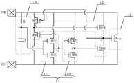
图1为一实施例中的静电放电保护电路的电路图;FIG. 1 is a circuit diagram of an electrostatic discharge protection circuit in an embodiment;
图2为一实施例中的静电放电保护电路在NS模式下静电保护的电路图。FIG. 2 is a circuit diagram of an ESD protection circuit in an NS mode of an ESD protection circuit according to an embodiment.
附图标记说明:Description of reference numbers:
10:脉冲检测单元,11:延迟单元,111:第一反相器,121:第二反相器,12:控制单元,13:泄放单元。10: Pulse detection unit, 11: Delay unit, 111: First inverter, 121: Second inverter, 12: Control unit, 13: Drain unit.
具体实施方式Detailed ways
为了便于理解本申请,下面将参照相关附图对本申请进行更全面的描述。附图中给出了本申请的首选实施例。但是,本申请可以以许多不同的形式来实现,并不限于本文所描述的实施例。相反地,提供这些实施例的目的是使对本申请的公开内容更加透彻全面。In order to facilitate understanding of the present application, the present application will be described more fully below with reference to the related drawings. Preferred embodiments of the present application are shown in the accompanying drawings. However, the application may be implemented in many different forms and is not limited to the embodiments described herein. Rather, these embodiments are provided so that this disclosure will be thorough and complete.
需要说明的是,当一个元件被认为是“连接”另一个元件,它可以是直接连接到另一个元件并与之结合为一体,或者可能同时存在居中元件。本文所使用的术语“安装”、“一端”、“另一端”以及类似的表述只是为了说明的目的。It should be noted that when an element is referred to as being "connected" to another element, it can be directly connected to and integrated with the other element, or intervening elements may also be present. The terms "installed," "one end," "the other end," and similar expressions used herein are for illustrative purposes only.
除非另有定义,本文所使用的所有的技术和科学术语与属于本申请的技术领域的技术人员通常理解的含义相同。本文中在本申请的说明书中所使用的术语只是为了描述具体的实施例的目的,不是旨在于限制本申请。本文所使用的术语“及/或”包括一个或多个相关的所列项目的任意的和所有的组合。Unless otherwise defined, all technical and scientific terms used herein have the same meaning as commonly understood by one of ordinary skill in the technical field to which this application belongs. The terms used herein in the specification of the present application are for the purpose of describing specific embodiments only and are not intended to limit the present application. As used herein, the term "and/or" includes any and all combinations of one or more of the associated listed items.
在一个实施例中,如图1所示,本发明一种静电放电保护电路,静电放电保护电路包括:脉冲检测单元10,脉冲检测单元10用于检测静电脉冲信号,其第一端连接第一电压VDD,第二端连接第二电压VSS,第三端输出脉冲检测信号;延迟单元11,延迟单元11用于延迟或增强所述脉冲检测信号的驱动能力,其第一端连接第一电压VDD,第二端连接第二电压VSS,第三端连接脉冲检测单元10的第三端,第四端输出第一延迟信号,第五端输出第二延迟信号;控制单元12,控制单元12用于根据第一延迟信号和第二延迟信号产生控制信号,其第一端连接第一电压VDD,第二端连接第二电压VSS,第三端连接延迟单元11的第五端,第四端连接延迟单元11的第四端,第五端输出控制信号;泄放单元13,泄放单元13用于根据控制信号打开或关闭静电电荷泄放通路,其第一端连接第一电压VDD,第二端连接第二电压VSS,第三端连接控制单元12的第五端。In one embodiment, as shown in FIG. 1 , an electrostatic discharge protection circuit of the present invention includes: a
上述静电放电保护电路在达到所需的静电保护效果的前提下具有较小的RC时间常数,静电放电保护电路的面积较小,不会占用较多的设计空间;同时可以避免噪声影响,提高静电保护电路的性能;上述静电放电保护电路还可以提供两种静电泄放模式的静电保护,有效地提高了产品的静电保护能力。The above electrostatic discharge protection circuit has a small RC time constant under the premise of achieving the required electrostatic protection effect. The area of the electrostatic discharge protection circuit is small and does not occupy a lot of design space; at the same time, it can avoid the influence of noise and improve the electrostatic discharge. The performance of the protection circuit; the above-mentioned electrostatic discharge protection circuit can also provide electrostatic protection in two electrostatic discharge modes, which effectively improves the electrostatic protection capability of the product.
在一个示例中,所检测单元10包括:电阻R和电容C,所述电阻R第一端作为脉冲检测单元10的第一端连接第一电压VDD,电阻R的第二端作为脉冲检测单元10的第三端,电容C的第一端连接电阻R的第二端,电容C的第二端作为脉冲检测单元10的第二端连接第二电压VSS。In one example, the
具体的,电阻R可以包括但不仅限于多晶硅电阻或掺杂区电阻。Specifically, the resistance R may include, but is not limited to, polysilicon resistance or doped region resistance.
具体的,电容C可以包括但不仅限于金属-介电层-金属电容或MOS电容。Specifically, the capacitor C may include, but is not limited to, a metal-dielectric layer-metal capacitor or a MOS capacitor.
具体的,电阻R的阻值和电容C的容值的乘积为一常数;更为具体的,电阻R的阻值和电容C的容值的乘积可以为0.01us~1us(微秒)。Specifically, the product of the resistance value of the resistor R and the capacitance value of the capacitor C is a constant; more specifically, the product of the resistance value of the resistor R and the capacitance value of the capacitor C may be 0.01us-1us (microseconds).
在一个示例中,延迟单元11包括:第一反相器111,第一反相器111的第一端作为延迟单元11的第三端与脉冲检测单元10的第三端相连接,第一反相器111的第二端连接第一电压VDD,第一反相器111的第三端连接第二电压VSS,第一反相器111的第四端作为延迟单元11的第四端;第二反相器121,第二反相器121的第一端与第一反相器111的第四端相连接,第二反相器121的第二端连接第一电压VDD,第二反相器121的第三端连接第二电压VSS;第二反相器121的第四端作为延迟单元11的第五端。In one example, the delay unit 11 includes: a
在一个示例中,第一反相器111包括第一PMOS管MP1及第一NMOS管MN1;第一PMOS管MP1的栅极与第一NMOS管MN1的栅极相连接共同作为第一反相器111的第一端,第一PMOS管MP1的源极作为第一反相器111的第二端连接第一电压VDD,第一PMOS管MP1的漏极与第一NMOS管MN1的漏极相连接共同作为第一反相器111的第四端;第一NMOS管MN1的源极作为第一反相器111的第三端连接第二电压VSS。In an example, the
在一个示例中,第二反相器121包括第二PMOS管MP2及第二NMOS管MN2;第二PMOS管MP2的栅极与第二NMOS管MN2的栅极相连接共同作第二反相器121的第一端与第一反相器的第四端相连接,第二PMOS管MP2的源极作为第二反相器121的第二端连接第一电压VDD,第二PMOS管MP2的漏极与第二NMOS管MN2的漏极相连接共同作为第二反相器121的第四端,第二NMOS管MN2的源极作为第二反相器121的第三端连接第二电压VSS。In an example, the
在一个示例中,控制单元12包括:第三PMOS管MP3,第三PMOS管MP3的源极连接第一电压VDD;第三NMOS管MN3,第三NMOS管MN3的栅极作为控制单元12的第四端与第一反相器111的第四端相连接,第三NMOS管MN3的漏极与第三PMOS管MP3的漏极相连接,第三NMOS管MN3的源极作为控制单元12的第二端连接第二电压VSS;第四PMOS管MP4,第四PMOS管MP4的栅极与第三PMOS管MP3的漏极及第三NMOS管MN3的漏极相连接,第四PMOS管MP4的源极连接第一电压VDD;第四NMOS管MN4,第四NMOS管MN4的栅极作为控制单元12的第三端与第二反相器121的第四端相连接,第四NMOS管MN4的漏极与第四PMOS管MP4的漏极及第三PMOS管MP3的栅极相连接以共同作为控制单元12的第五端。In one example, the
在一个示例中,泄放单元13可以包括泄放晶体管MEDS,具体的,泄放晶体管MEDS可以为NMOS管。泄放晶体管MEDS的漏极作为泄放单元13的第一端连接第一电压VDD,泄放晶体管MEDS的源极作为泄放单元13的第二端连接第二电压VSS,泄放晶体管MEDS的栅极作为泄放单元13的第三端与控制单元12的第五端相连接。In one example, the
图1所示的静电放电保护电路的工作原理为:The working principle of the ESD protection circuit shown in Figure 1 is:
正常工作时,脉冲检测单元10的第三端(即图1中的a端)为高电平,经过包括第一PMOS管MP1及第一NMOS管MN1的第一反相器111后,第一反相器111的第四端(即图1中的c端)为低电平,在经过包括第二PMOS管MP2及第二NMOS管MN2的第二反相器121后,第二反相器121的第四端(即图1中的d端)为高电平,此时,第四NMOS管MN4打开使得控制单元12的第五端(即图1中的e端)为低电平,从而确保泄放晶体管MEDS关掉;同时,由于控制单元12的第五端为低电平,经过反馈后可以使得图中的b端为高电平,第四PMOS管MP4被关掉,从而更好地确保控制单元12的第五端为低电平,进一步确保泄放晶体管MEDS不漏电。During normal operation, the third terminal of the pulse detection unit 10 (ie terminal a in FIG. 1 ) is at a high level. After passing through the
在PS模式(VSS接地,在VDD上产生正向静电脉冲)静电发生时,脉冲检测单元10的第三端(即图1中的a端)为低电平,经过包括第一PMOS管MP1及第一NMOS管MN1的第一反相器111后,第一反相器111的第四端(即图1中的c端)为高电平,在经过包括第二PMOS管MP2及第二NMOS管MN2的第二反相器121后,第二反相器121的第四端(即图1中的d端)为低电平,此时,第四NMOS管MN4关掉;由于第一反相器111的第四端(即图1中的c端)为高电平,第三NMOS管MN3导通,图1中的b端为低电平,第四PMOS管MP4导通,使得控制单元12的第五端(即图1中的e端)为高电平,从而确保泄放晶体管MEDS导通泄放静电电流。随着ESD作用时间的增加,脉冲检测单元10的第三端(即图1中的a端)的电位逐渐升高,经过延迟单元11,d点电位也逐渐升高,e点电位逐渐降低,从而b点电位逐渐升高,但是由于c点电位逐渐降低,又使得b点电位逐渐降低,即在ESD作用时间增加的过程中,b点电位既有上拉作用也有下拉作用,从而使得b点降低过程被延迟,进而延迟了e点电位降低的过程。在ESD作用时间增加的过程中,静电放电保护电路能够延长图1中的e端维持为高电平的时间,从而可以实现小的RC时间常数的同时保证泄放晶体管MEDS在静电作用的时间内有有效导通泄放静电电流。In PS mode (VSS is grounded, and positive electrostatic pulse is generated on VDD), when static electricity occurs, the third terminal of the pulse detection unit 10 (ie, terminal a in FIG. 1 ) is at a low level. After the
在NS模式(VSS接地,在VDD上产生负向脉冲)静电发生时,如图2所示,经由泄放晶体管MEDS所形成的寄生二极管Dp泄放静电电流,从而可以实现NS模式下的静电放电保护。When static electricity occurs in NS mode (VSS is grounded, and a negative pulse is generated on VDD), as shown in Figure 2, the static current is discharged through the parasitic diode Dp formed by the discharge transistor MEDS , so that static electricity in NS mode can be realized. Discharge protection.
上所述实施例的各技术特征可以进行任意的组合,为使描述简洁,未对上述实施例各个技术特征所有可能的组合都进行描述,然而,只要这些技术特征的组合不存在矛盾,都应当认为是本说明书记载的范围。The technical features of the above-described embodiments can be combined arbitrarily. In order to make the description concise, all possible combinations of the technical features of the above-described embodiments are not described. However, as long as there is no contradiction in the combination of these technical features, it should be It is considered to be the range described in this specification.
以上所述实施例仅表达了本申请的几种实施方式,其描述较为具体和详细,但并不能因此而理解为对申请专利范围的限制。应当指出的是,对于本领域的普通技术人员来说,在不脱离本申请构思的前提下,还可以做出若干变形和改进,这些都属于本申请的保护范围。因此,本申请专利的保护范围应以所附权利要求为准。The above-mentioned embodiments only represent several embodiments of the present application, and the descriptions thereof are relatively specific and detailed, but should not be construed as a limitation on the scope of the patent application. It should be pointed out that for those skilled in the art, without departing from the concept of the present application, several modifications and improvements can be made, which all belong to the protection scope of the present application. Therefore, the scope of protection of the patent of the present application shall be subject to the appended claims.
Claims (9)
Translated fromChinesePriority Applications (4)
| Application Number | Priority Date | Filing Date | Title |
|---|---|---|---|
| CN202010224088.0ACN113451293B (en) | 2020-03-26 | 2020-03-26 | Electrostatic discharge protection circuit |
| EP21774448.1AEP3975248B1 (en) | 2020-03-26 | 2021-03-08 | Electrostatic discharge protection circuit |
| PCT/CN2021/079537WO2021190286A1 (en) | 2020-03-26 | 2021-03-08 | Electrostatic discharge protection circuit |
| US17/376,112US12224280B2 (en) | 2020-03-26 | 2021-07-14 | Electrostatic discharge protection circuit including a pulse detection circuit |
Applications Claiming Priority (1)
| Application Number | Priority Date | Filing Date | Title |
|---|---|---|---|
| CN202010224088.0ACN113451293B (en) | 2020-03-26 | 2020-03-26 | Electrostatic discharge protection circuit |
Publications (2)
| Publication Number | Publication Date |
|---|---|
| CN113451293A CN113451293A (en) | 2021-09-28 |
| CN113451293Btrue CN113451293B (en) | 2022-05-27 |
Family
ID=77807152
Family Applications (1)
| Application Number | Title | Priority Date | Filing Date |
|---|---|---|---|
| CN202010224088.0AActiveCN113451293B (en) | 2020-03-26 | 2020-03-26 | Electrostatic discharge protection circuit |
Country Status (4)
| Country | Link |
|---|---|
| US (1) | US12224280B2 (en) |
| EP (1) | EP3975248B1 (en) |
| CN (1) | CN113451293B (en) |
| WO (1) | WO2021190286A1 (en) |
Families Citing this family (7)
| Publication number | Priority date | Publication date | Assignee | Title |
|---|---|---|---|---|
| CN113985163B (en)* | 2021-10-15 | 2024-04-30 | 深圳市爱协生科技股份有限公司 | ESD detection circuit, integrated circuit, and electronic device |
| TWI779942B (en)* | 2021-11-30 | 2022-10-01 | 瑞昱半導體股份有限公司 | Electrical discharge circuit having stable discharging mechanism |
| CN116247633B (en)* | 2021-12-08 | 2025-08-12 | 瑞昱半导体股份有限公司 | Static protection circuit with stable discharge mechanism |
| TWI792767B (en)* | 2021-12-14 | 2023-02-11 | 瑞昱半導體股份有限公司 | Electrical discharge circuit having stable discharging mechanism |
| US12132308B2 (en)* | 2022-04-11 | 2024-10-29 | Changxin Memory Technologies, Inc. | Electrostatic protection circuit |
| TWI806588B (en)* | 2022-05-05 | 2023-06-21 | 瑞昱半導體股份有限公司 | The novel voltage detection power clamp circuit for power eos event |
| TWI847627B (en)* | 2023-03-24 | 2024-07-01 | 瑞昱半導體股份有限公司 | Electrical discharge circuit |
Citations (6)
| Publication number | Priority date | Publication date | Assignee | Title |
|---|---|---|---|---|
| CN1501757A (en)* | 2002-11-15 | 2004-06-02 | 华邦电子股份有限公司 | Electrostatic protection circuit using grid coupling metal-oxide half field effect transistor |
| CN1596058A (en)* | 2003-09-08 | 2005-03-16 | 联发科技股份有限公司 | Electrostatic discharge protection circuit |
| CN101197500A (en)* | 2006-12-08 | 2008-06-11 | 智原科技股份有限公司 | Electrostatic discharge protection circuit |
| CN101707363A (en)* | 2009-07-22 | 2010-05-12 | 彩优微电子(昆山)有限公司 | Electrostatic damage protection circuit having real-time detection function, and control method thereof |
| CN103646945A (en)* | 2013-12-03 | 2014-03-19 | 北京中电华大电子设计有限责任公司 | Integrated circuit power supply esd protection circuit |
| CN108878416A (en)* | 2018-06-28 | 2018-11-23 | 武汉新芯集成电路制造有限公司 | ESD protection circuit |
Family Cites Families (20)
| Publication number | Priority date | Publication date | Assignee | Title |
|---|---|---|---|---|
| US6912109B1 (en)* | 2000-06-26 | 2005-06-28 | Taiwan Semiconductor Manufacturing Co., Ltd. | Power-rail ESD clamp circuits with well-triggered PMOS |
| US20050035806A1 (en)* | 2003-07-24 | 2005-02-17 | El-Sherif Alaa Y. | Circuit and method to protect EEPROM data during ESD events |
| US7085113B2 (en)* | 2004-08-20 | 2006-08-01 | International Business Machines Corporation | ESD protection power clamp for suppressing ESD events occurring on power supply terminals |
| US7453676B2 (en)* | 2005-11-16 | 2008-11-18 | Huh Yoon J | RC-triggered ESD power clamp circuit and method for providing ESD protection |
| US20070171587A1 (en)* | 2006-01-26 | 2007-07-26 | Chien-Ming Lee | Esd protection circuit with feedback technique |
| CN101060754A (en) | 2006-04-20 | 2007-10-24 | 矽统科技股份有限公司 | ESD protection circuit with feedback technology |
| KR100814437B1 (en)* | 2006-11-03 | 2008-03-17 | 삼성전자주식회사 | Hybrid Electrostatic Discharge Protection Circuit |
| US7760476B2 (en)* | 2007-06-07 | 2010-07-20 | Atmel Corporation | Threshold voltage method and apparatus for ESD protection |
| WO2009023099A2 (en) | 2007-08-10 | 2009-02-19 | Skyworks Solutions, Inc. | Power clamp for on-chip esd protection |
| DE102008006963B4 (en) | 2008-01-31 | 2015-07-30 | Globalfoundries Inc. | ESD power clamping device with stable switch-on function |
| US8369054B2 (en) | 2010-06-08 | 2013-02-05 | Hong Kong Applied Science And Technology Research Institute Co., Ltd. | NMOS-based feedback power-clamp for on-chip ESD protection |
| WO2013051175A1 (en)* | 2011-10-06 | 2013-04-11 | パナソニック株式会社 | Semiconductor integrated circuit device |
| CN103078305B (en)* | 2013-01-09 | 2015-02-04 | 北京大学 | Anti-false-triggering power supply clamp ESD (Electro-Static Discharge) protection circuit |
| US20150084702A1 (en)* | 2013-09-26 | 2015-03-26 | Triquint Semiconductor, Inc. | Electrostatic discharge (esd) circuitry |
| CN105098743B (en)* | 2014-05-04 | 2018-09-18 | 中芯国际集成电路制造(上海)有限公司 | Dynamic electrostatic electric discharge clamp circuit |
| US9356442B2 (en)* | 2014-07-08 | 2016-05-31 | Hong Kong Applied Science and Technology Research Institute Company, Limited | Area-efficient clamp for power ring ESD protection using a transmission gate |
| US10594135B2 (en)* | 2017-06-29 | 2020-03-17 | Dialog Semiconductor (Uk) Limited | Compact, high performance, and robust RC triggered ESD clamp |
| US11056481B2 (en)* | 2018-08-13 | 2021-07-06 | Amazing Microelectronic Corp. | Floating base silicon controlled rectifier |
| CN209823413U (en)* | 2019-04-22 | 2019-12-20 | 长鑫存储技术有限公司 | Electrostatic discharge protection circuit and integrated circuit chip |
| CN115173384A (en)* | 2021-04-01 | 2022-10-11 | 长鑫存储技术有限公司 | Electrostatic protection circuit |
- 2020
- 2020-03-26CNCN202010224088.0Apatent/CN113451293B/enactiveActive
- 2021
- 2021-03-08WOPCT/CN2021/079537patent/WO2021190286A1/ennot_activeCeased
- 2021-03-08EPEP21774448.1Apatent/EP3975248B1/enactiveActive
- 2021-07-14USUS17/376,112patent/US12224280B2/enactiveActive
Patent Citations (6)
| Publication number | Priority date | Publication date | Assignee | Title |
|---|---|---|---|---|
| CN1501757A (en)* | 2002-11-15 | 2004-06-02 | 华邦电子股份有限公司 | Electrostatic protection circuit using grid coupling metal-oxide half field effect transistor |
| CN1596058A (en)* | 2003-09-08 | 2005-03-16 | 联发科技股份有限公司 | Electrostatic discharge protection circuit |
| CN101197500A (en)* | 2006-12-08 | 2008-06-11 | 智原科技股份有限公司 | Electrostatic discharge protection circuit |
| CN101707363A (en)* | 2009-07-22 | 2010-05-12 | 彩优微电子(昆山)有限公司 | Electrostatic damage protection circuit having real-time detection function, and control method thereof |
| CN103646945A (en)* | 2013-12-03 | 2014-03-19 | 北京中电华大电子设计有限责任公司 | Integrated circuit power supply esd protection circuit |
| CN108878416A (en)* | 2018-06-28 | 2018-11-23 | 武汉新芯集成电路制造有限公司 | ESD protection circuit |
Also Published As
| Publication number | Publication date |
|---|---|
| EP3975248B1 (en) | 2023-12-20 |
| US12224280B2 (en) | 2025-02-11 |
| EP3975248A1 (en) | 2022-03-30 |
| WO2021190286A1 (en) | 2021-09-30 |
| CN113451293A (en) | 2021-09-28 |
| US20210343702A1 (en) | 2021-11-04 |
| EP3975248A4 (en) | 2022-11-02 |
Similar Documents
| Publication | Publication Date | Title |
|---|---|---|
| CN113451293B (en) | Electrostatic discharge protection circuit | |
| JP5955924B2 (en) | Electrostatic discharge protection circuit | |
| US9425616B2 (en) | RC triggered ESD protection device | |
| CN110957713B (en) | Electrostatic discharge clamping circuit | |
| US8810982B2 (en) | Semiconductor integrated circuit and protection circuit | |
| CN211830608U (en) | Circuit including NMOS transistor having body dynamically coupled to drain | |
| TW201507307A (en) | ESD clamp circuit | |
| JP2014132717A (en) | Electrostatic discharge protection circuit and semiconductor circuit device | |
| CN102801146A (en) | Power clamp ESD (Electronic Static Discharge) protective circuit | |
| US10177135B2 (en) | Integrated circuit and electrostatic discharge protection circuit thereof | |
| US9614368B2 (en) | Area-efficient active-FET ESD protection circuit | |
| CN109449156B (en) | Port electrostatic discharge protection circuit | |
| US20180182749A1 (en) | Dynamically triggered electrostatic discharge cell | |
| KR100313154B1 (en) | Electrostatic discharge protection circuit | |
| CN112448378A (en) | Electrostatic protection circuit | |
| CN100568659C (en) | Electrostatic discharge protection circuit | |
| TWI806588B (en) | The novel voltage detection power clamp circuit for power eos event | |
| TWI823291B (en) | Protection circuit | |
| CN113452004B (en) | Electrostatic protection circuit and full-chip electrostatic protection circuit | |
| CN110379856B (en) | MOS-D transistor and ESD protection circuit formed by same | |
| JP2005516443A (en) | Voltage limited semiconductor pass gate circuit | |
| CN110880861A (en) | An electrostatic protection circuit in the Internet of Things | |
| WO2022188326A1 (en) | Electrostatic protection circuit and semiconductor device | |
| CN116845842A (en) | Protection circuit | |
| JPH08204125A (en) | Semiconductor circuit |
Legal Events
| Date | Code | Title | Description |
|---|---|---|---|
| PB01 | Publication | ||
| PB01 | Publication | ||
| SE01 | Entry into force of request for substantive examination | ||
| SE01 | Entry into force of request for substantive examination | ||
| GR01 | Patent grant | ||
| GR01 | Patent grant |