CN113433094B - Biosensor for realizing FP-WA coupling mode and preparation method and application thereof - Google Patents
Biosensor for realizing FP-WA coupling mode and preparation method and application thereofDownload PDFInfo
- Publication number
- CN113433094B CN113433094BCN202110510078.8ACN202110510078ACN113433094BCN 113433094 BCN113433094 BCN 113433094BCN 202110510078 ACN202110510078 ACN 202110510078ACN 113433094 BCN113433094 BCN 113433094B
- Authority
- CN
- China
- Prior art keywords
- groove
- metal
- metal layer
- biosensor
- dielectric
- Prior art date
- Legal status (The legal status is an assumption and is not a legal conclusion. Google has not performed a legal analysis and makes no representation as to the accuracy of the status listed.)
- Active
Links
Images


Classifications
- G—PHYSICS
- G01—MEASURING; TESTING
- G01N—INVESTIGATING OR ANALYSING MATERIALS BY DETERMINING THEIR CHEMICAL OR PHYSICAL PROPERTIES
- G01N33/00—Investigating or analysing materials by specific methods not covered by groups G01N1/00 - G01N31/00
- G01N33/48—Biological material, e.g. blood, urine; Haemocytometers
- G01N33/50—Chemical analysis of biological material, e.g. blood, urine; Testing involving biospecific ligand binding methods; Immunological testing
- G01N33/53—Immunoassay; Biospecific binding assay; Materials therefor
- G01N33/543—Immunoassay; Biospecific binding assay; Materials therefor with an insoluble carrier for immobilising immunochemicals
- G01N33/54366—Apparatus specially adapted for solid-phase testing
- G01N33/54373—Apparatus specially adapted for solid-phase testing involving physiochemical end-point determination, e.g. wave-guides, FETS, gratings
- G—PHYSICS
- G01—MEASURING; TESTING
- G01N—INVESTIGATING OR ANALYSING MATERIALS BY DETERMINING THEIR CHEMICAL OR PHYSICAL PROPERTIES
- G01N21/00—Investigating or analysing materials by the use of optical means, i.e. using sub-millimetre waves, infrared, visible or ultraviolet light
- G01N21/17—Systems in which incident light is modified in accordance with the properties of the material investigated
- G01N21/55—Specular reflectivity
- G01N21/552—Attenuated total reflection
- G01N21/553—Attenuated total reflection and using surface plasmons
- G—PHYSICS
- G01—MEASURING; TESTING
- G01N—INVESTIGATING OR ANALYSING MATERIALS BY DETERMINING THEIR CHEMICAL OR PHYSICAL PROPERTIES
- G01N21/00—Investigating or analysing materials by the use of optical means, i.e. using sub-millimetre waves, infrared, visible or ultraviolet light
- G01N21/01—Arrangements or apparatus for facilitating the optical investigation
- G—PHYSICS
- G01—MEASURING; TESTING
- G01N—INVESTIGATING OR ANALYSING MATERIALS BY DETERMINING THEIR CHEMICAL OR PHYSICAL PROPERTIES
- G01N21/00—Investigating or analysing materials by the use of optical means, i.e. using sub-millimetre waves, infrared, visible or ultraviolet light
- G01N21/17—Systems in which incident light is modified in accordance with the properties of the material investigated
- G01N21/55—Specular reflectivity
- G01N21/552—Attenuated total reflection
- G01N21/553—Attenuated total reflection and using surface plasmons
- G01N21/554—Attenuated total reflection and using surface plasmons detecting the surface plasmon resonance of nanostructured metals, e.g. localised surface plasmon resonance
- G—PHYSICS
- G01—MEASURING; TESTING
- G01N—INVESTIGATING OR ANALYSING MATERIALS BY DETERMINING THEIR CHEMICAL OR PHYSICAL PROPERTIES
- G01N33/00—Investigating or analysing materials by specific methods not covered by groups G01N1/00 - G01N31/00
- G01N33/48—Biological material, e.g. blood, urine; Haemocytometers
- G01N33/50—Chemical analysis of biological material, e.g. blood, urine; Testing involving biospecific ligand binding methods; Immunological testing
- G01N33/68—Chemical analysis of biological material, e.g. blood, urine; Testing involving biospecific ligand binding methods; Immunological testing involving proteins, peptides or amino acids
- G01N33/689—Chemical analysis of biological material, e.g. blood, urine; Testing involving biospecific ligand binding methods; Immunological testing involving proteins, peptides or amino acids related to pregnancy or the gonads
- G—PHYSICS
- G01—MEASURING; TESTING
- G01N—INVESTIGATING OR ANALYSING MATERIALS BY DETERMINING THEIR CHEMICAL OR PHYSICAL PROPERTIES
- G01N21/00—Investigating or analysing materials by the use of optical means, i.e. using sub-millimetre waves, infrared, visible or ultraviolet light
- G01N21/01—Arrangements or apparatus for facilitating the optical investigation
- G01N2021/0106—General arrangement of respective parts
- G01N2021/0112—Apparatus in one mechanical, optical or electronic block
- G—PHYSICS
- G01—MEASURING; TESTING
- G01N—INVESTIGATING OR ANALYSING MATERIALS BY DETERMINING THEIR CHEMICAL OR PHYSICAL PROPERTIES
- G01N2333/00—Assays involving biological materials from specific organisms or of a specific nature
- G01N2333/435—Assays involving biological materials from specific organisms or of a specific nature from animals; from humans
- G01N2333/46—Assays involving biological materials from specific organisms or of a specific nature from animals; from humans from vertebrates
- G01N2333/47—Assays involving proteins of known structure or function as defined in the subgroups
- G01N2333/4701—Details
- G01N2333/471—Pregnancy proteins, e.g. placenta proteins, alpha-feto-protein, pregnancy specific beta glycoprotein
- G—PHYSICS
- G01—MEASURING; TESTING
- G01N—INVESTIGATING OR ANALYSING MATERIALS BY DETERMINING THEIR CHEMICAL OR PHYSICAL PROPERTIES
- G01N2800/00—Detection or diagnosis of diseases
- G01N2800/38—Pediatrics
- G01N2800/385—Congenital anomalies
Landscapes
- Health & Medical Sciences (AREA)
- Life Sciences & Earth Sciences (AREA)
- Immunology (AREA)
- Chemical & Material Sciences (AREA)
- Engineering & Computer Science (AREA)
- Analytical Chemistry (AREA)
- Biochemistry (AREA)
- General Health & Medical Sciences (AREA)
- General Physics & Mathematics (AREA)
- Pathology (AREA)
- Physics & Mathematics (AREA)
- Hematology (AREA)
- Urology & Nephrology (AREA)
- Molecular Biology (AREA)
- Biomedical Technology (AREA)
- Biotechnology (AREA)
- Cell Biology (AREA)
- Microbiology (AREA)
- Food Science & Technology (AREA)
- Medicinal Chemistry (AREA)
- Pregnancy & Childbirth (AREA)
- Gynecology & Obstetrics (AREA)
- Proteomics, Peptides & Aminoacids (AREA)
- Reproductive Health (AREA)
- Nanotechnology (AREA)
- Investigating Or Analysing Materials By Optical Means (AREA)
Abstract
Description
Translated fromChinese技术领域technical field
本发明涉及传感器技术领域,尤其是涉及一种实现FP-WA耦合模式的生物传感器及其制备方法和应用。The invention relates to the technical field of sensors, in particular to a biosensor for realizing FP-WA coupling mode and its preparation method and application.
背景技术Background technique
随着全球医疗模式开始由“集中化”向“分散化”转变以及数字化远程医疗的普及,生物医学检测的应用场景也逐渐从大型医院扩大到了社区、交通枢纽和家庭。传统的生物医学检测主要通过将收集的样本(血液、尿液或遗传样本等)送到现场以外的分析实验室进行检验。而如今,利用基于生物传感器的即时检测(point-of-care testing,POCT)设备,在采样现场即刻进行分析,可以省去标本在实验室检验时的复杂处理程序,快速得到检验结果。With the transformation of the global medical model from "centralization" to "decentralization" and the popularization of digital telemedicine, the application scenarios of biomedical testing have gradually expanded from large hospitals to communities, transportation hubs and families. Traditional biomedical testing is mainly carried out by sending collected samples (blood, urine or genetic samples, etc.) to analytical laboratories off-site. Today, using point-of-care testing (POCT) equipment based on biosensors, analysis can be performed immediately at the sampling site, which can save the complicated processing procedures of specimens in the laboratory and quickly obtain test results.
在这种趋势下,高灵敏、低成本、快速和便携性成为新一代生物传感器的追求目标。其中,表面等离激元(Surface plasmon resonance,SPR)传感作为上世纪90年代初新兴的一种生物分子传感技术,可以提供一种灵敏、简捷、快速、集成化的生物医学检测解决方案。在SPR传感技术中,主要可以分为两种:传统的基于传播表面等离激元(Propagatingsurface plasmon resonance,PSPR),以及基于局域表面等离激元(Localized surfaceplasmon resonance,LSPR)。然而,尽管PSPR具有良好的灵敏性,但是其需要依赖复杂的设备和高昂的成本,难以由“集中化”向“分散化”转变。LSPR结构较为简单,但是其谐振峰的线宽比较大、品质因子较低。Under this trend, high sensitivity, low cost, speed and portability have become the pursuit goals of a new generation of biosensors. Among them, surface plasmon resonance (SPR) sensing, as a new biomolecular sensing technology in the early 1990s, can provide a sensitive, simple, fast and integrated biomedical detection solution . In SPR sensing technology, it can be mainly divided into two types: traditional based on propagating surface plasmon resonance (PSPR), and based on localized surface plasmon resonance (LSPR). However, although PSPR has good sensitivity, it needs to rely on complex equipment and high cost, making it difficult to transform from "centralization" to "decentralization". The structure of LSPR is relatively simple, but the line width of its resonance peak is relatively large and the quality factor is low.
发明内容Contents of the invention
基于此,有必要提供一种结构简单、谐振峰线宽小以及品质因子高的实现FP-WA耦合模式的生物传感器及其制备方法和应用。Based on this, it is necessary to provide a biosensor capable of realizing FP-WA coupling mode with simple structure, small resonant peak line width and high quality factor, as well as its preparation method and application.
为了解决以上技术问题,本发明的技术方案为:In order to solve the above technical problems, the technical solution of the present invention is:
一种实现FP-WA耦合模式的生物传感器,包括介质层和金属层;所述介质层具有多个介质凹槽,多个所述介质凹槽周期性等间距分布,所述介质凹槽在自其槽口到槽底的方向上的开口宽度逐渐减小;所述金属层设在所述介质层之上并对应各所述介质凹槽形成金属凹槽;A biosensor for realizing the FP-WA coupling mode, comprising a dielectric layer and a metal layer; the dielectric layer has a plurality of dielectric grooves, and a plurality of the dielectric grooves are periodically distributed at equal intervals, and the dielectric grooves are automatically The opening width from the notch to the groove bottom gradually decreases; the metal layer is arranged on the dielectric layer and forms a metal groove corresponding to each of the dielectric grooves;
所述金属凹槽的周期满足式(1):The period of the metal groove satisfies formula (1):

所述金属凹槽的深度、所述金属凹槽的槽口宽度以及所述金属凹槽的槽底宽度满足式(2):The depth of the metal groove, the notch width of the metal groove and the groove bottom width of the metal groove satisfy formula (2):

其中,
a代表所述金属凹槽的周期,h代表所述金属凹槽的深度,w0代表所述金属凹槽的槽口宽度,w1代表所述金属凹槽的槽底宽度,i代表WA模式的阶数,λWA代表WA模式的谐振波长,m代表FP模式的阶数,λWG代表FP模式的谐振波长,k代表FP模式的谐振波数,
在其中一个实施例中,所述金属凹槽的周期为600nm~1500nm,所述金属凹槽的深度为300nm~800nm,所述金属凹槽的槽口宽度为400nm~600nm,所述金属凹槽的槽底宽度为200nm~400nm。In one embodiment, the period of the metal groove is 600nm-1500nm, the depth of the metal groove is 300nm-800nm, the slot width of the metal groove is 400nm-600nm, the metal groove The groove bottom width is 200nm-400nm.
在其中一个实施例中,所述生物传感器的谐振线宽为3nm~9nm。In one of the embodiments, the resonance linewidth of the biosensor is 3nm-9nm.
在其中一个实施例中,所述金属层的厚度为200nm~500nm。In one embodiment, the metal layer has a thickness of 200nm-500nm.
在其中一个实施例中,所述金属层的表面粗糙度的均方根为0.2nm~1.9nm。In one embodiment, the root mean square of the surface roughness of the metal layer is 0.2 nm˜1.9 nm.
在其中一个实施例中,多个介质凹槽呈多行多列分布,各行相互平行,各列相互平行,且各行与各列相互垂直。In one embodiment, the plurality of dielectric grooves are distributed in multiple rows and columns, each row is parallel to each other, each column is parallel to each other, and each row and each column are perpendicular to each other.
在其中一个实施例中,各行的介质凹槽相连通以形成宽度均匀的连通凹槽;或者,各列的介质凹槽相连通各行的介质凹槽相连通以形成宽度均匀的连通凹槽。In one embodiment, the dielectric grooves of each row are connected to form a communication groove of uniform width; or, the dielectric grooves of each column are connected to the dielectric grooves of each row to form a communication groove of uniform width.
在其中一个实施例中,所述生物传感器还包括衬底,所述衬底设于所述介质层的远离所述金属层的表面。In one of the embodiments, the biosensor further includes a substrate, and the substrate is provided on the surface of the dielectric layer away from the metal layer.
在其中一个实施例中,所述金属层为金层、铂层以及银层中至少一种。In one embodiment, the metal layer is at least one of a gold layer, a platinum layer and a silver layer.
在其中一个实施例中,所述介质层为热固化环氧树脂介质层或光固化环氧树脂介质层。In one embodiment, the medium layer is a heat-cured epoxy resin medium layer or a light-cured epoxy resin medium layer.
上述任一实施例中所述的生物传感器的制备方法,包括如下步骤:The preparation method of the biosensor described in any of the above-mentioned embodiments comprises the following steps:
在模板上形成周期性等间距分布的辅助凸起;Auxiliary bumps distributed periodically and equally spaced are formed on the template;
在所述模板的表面形成金属层,所述金属层对应各所述辅助凸起形成所述金属凹槽;forming a metal layer on the surface of the template, the metal layer corresponding to each of the auxiliary protrusions to form the metal groove;
在所述金属层之上形成所述介质层;forming the dielectric layer over the metal layer;
分离所述金属层与所述模板。separating the metal layer from the template.
在其中一个实施例中,所述模板为硅片。In one embodiment, the template is a silicon wafer.
上述任一实施例中所述的生物传感器以非疾病诊断目的在目标物感兴趣参数检测中的应用。The application of the biosensor described in any of the above embodiments in the detection of parameters of interest of a target object for non-disease diagnosis purposes.
在其中一个实施例中,所述应用包括如下步骤:In one of the embodiments, the application includes the following steps:
将入射光沿垂直于金属凹槽的槽底的方向入射到金属层的表面,测量反射光的初始光学参数;The incident light is incident on the surface of the metal layer along the direction perpendicular to the groove bottom of the metal groove, and the initial optical parameters of the reflected light are measured;
在金属层表面分别滴加不同已知感兴趣参数的目标物溶液,并测量该溶液对应的反射光的标准光学参数;Dropping target solutions with different known parameters of interest on the surface of the metal layer, and measuring the standard optical parameters of the reflected light corresponding to the solution;
分别计算各不同已知感兴趣参数的溶液对应的标准光学参数与所述初始光学参数的差值,并基于该差值与对应的已知感兴趣参数获取光学参数随溶液感兴趣参数的变化关系;Calculate the difference between the standard optical parameters corresponding to the solutions with different known parameters of interest and the initial optical parameters, and obtain the relationship between the optical parameters and the parameters of interest in the solution based on the difference and the corresponding known parameters of interest ;
在金属层表面滴加待测溶液,测试所述待测溶液对应的反射光的样品光学参数,并计算该样品光学参数与所述初始光学参数的差值,进而根据该差值与所述变化关系获取所述待测溶液的感兴趣参数。Drop the solution to be tested on the surface of the metal layer, test the sample optical parameters of the reflected light corresponding to the solution to be tested, and calculate the difference between the sample optical parameters and the initial optical parameters, and then according to the difference and the change The relationship obtains the parameter of interest of the solution to be tested.
在其中一个实施例中,多个介质凹槽呈多行多列分布,各行相互平行,各列相互平行,且各行与各列相互垂直;所述入射光的偏振方向与行方向垂直,或者所述入射光的偏振方向与列方向垂直。In one of the embodiments, the plurality of dielectric grooves are distributed in multiple rows and columns, each row is parallel to each other, each column is parallel to each other, and each row and each column are perpendicular to each other; the polarization direction of the incident light is perpendicular to the row direction, or the polarization direction of the incident light is perpendicular to the row direction, or the The polarization direction of the incident light is perpendicular to the column direction.
在其中一个实施例中,各行的介质凹槽相连通以形成宽度均匀的连通凹槽;或者,各列的介质凹槽相连通以形成宽度均匀的连通凹槽;所述入射光的偏振方向与所述连通凹槽的延伸方向垂直。In one of the embodiments, the dielectric grooves in each row are connected to form a connected groove with a uniform width; or, the dielectric grooves in each column are connected to form a connected groove with a uniform width; the polarization direction of the incident light and The extending direction of the communication groove is vertical.
在其中一个实施例中,所述目标物为盐、有机溶剂、抗原、抗体、DNA或RNA。In one embodiment, the target is salt, organic solvent, antigen, antibody, DNA or RNA.
上述生物传感器中,通过对结构进行设置,在介质层上形成多个周期性等间距分布的金属凹槽,每个金属凹槽相当于一个谐振器,在金属凹槽里面支持一种线宽较宽的法布里-珀罗腔模式(FP模式),同时,金属凹槽的周期性诱导了伍德异常(Wood’anomaly)模式(WA模式)。根据式(1)和式(2)中的结构参数和谐振波长的关系来对金属凹槽的周期、金属凹槽的深度、金属凹槽的槽口宽度以及金属凹槽的槽底宽度进行设定,使得FP模式和WA模式的波长互相靠近,得到一种极窄线宽和极深反射谷的耦合模式,即FP-WA耦合模式,进而得到了一种谐振峰线宽小、品质因子高的生物传感器。同时,上述生物传感器结构简单,FP-WA耦合模式可以在垂直入射下激发,因此避免了基于斜入射激发的生物传感器所需的高精度角度调节组件,更加利于器件集成,便于转运和使用,能够有效促进生物检测由“集中化”向“分散化”转变。In the above-mentioned biosensor, by setting the structure, a plurality of metal grooves distributed at regular intervals are formed on the dielectric layer. Each metal groove is equivalent to a resonator, and a metal groove with a relatively wide line width is supported in the metal groove. Wide Fabry-Perot cavity modes (FP modes), meanwhile, the periodicity of metal grooves induces Wood'anomaly modes (WA modes). According to the relationship between the structural parameters and the resonance wavelength in formula (1) and formula (2), the period of the metal groove, the depth of the metal groove, the width of the notch of the metal groove and the width of the bottom of the metal groove are set. fixed, so that the wavelengths of the FP mode and the WA mode are close to each other, and a coupling mode with an extremely narrow linewidth and a deep reflection valley is obtained, that is, the FP-WA coupling mode, and then a resonance peak with a small linewidth and a high quality factor is obtained. biosensors. At the same time, the above-mentioned biosensor has a simple structure, and the FP-WA coupling mode can be excited under normal incidence, thus avoiding the high-precision angle adjustment components required by biosensors based on oblique incidence excitation, which is more conducive to device integration, easy to transport and use, and can Effectively promote the transformation of biological detection from "centralization" to "decentralization".
上述生物传感器的制备方法中,通过先在模板上形成周期性的辅助凸起,然后在辅助凸起的表面形成金属层,以形成金属凹槽,再在金属层的表面形成介质层,接着再分离金属层和模板。采用上述制备方法能够使金属层与模板具有同样的光滑表面,能够有效提高金属层的光滑性,这样就可以进一步降低谐振峰线宽、提高品质因子。同时采用上述制备方法能够有效避免金属层厚度变化和金属层不对称而影响生物传感器的光学响应等问题。In the preparation method of the above-mentioned biosensor, by first forming periodic auxiliary protrusions on the template, then forming a metal layer on the surface of the auxiliary protrusions to form metal grooves, and then forming a dielectric layer on the surface of the metal layer, and then Separate the metal layer and template. Adopting the above preparation method can make the metal layer have the same smooth surface as the template, and can effectively improve the smoothness of the metal layer, so that the resonance peak line width can be further reduced and the quality factor can be improved. At the same time, adopting the above preparation method can effectively avoid problems such as changes in the thickness of the metal layer and asymmetry of the metal layer affecting the optical response of the biosensor.
上述生物传感器以非疾病诊断目的在目标物感兴趣参数检测中的应用操作方便易行,不需要依赖高波长分辨率的探测器,检测成本低。The application of the above-mentioned biosensor in the detection of the parameters of interest of the target object for the purpose of non-disease diagnosis is convenient and easy to operate, does not need to rely on detectors with high wavelength resolution, and the detection cost is low.
附图说明Description of drawings
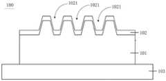
图1为本发明一实施例中生物传感器的结构示意图;Fig. 1 is a schematic structural diagram of a biosensor in an embodiment of the present invention;
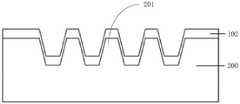
图2为图1对应的生物传感器中金属凹槽的尺寸标记;Fig. 2 is the size mark of the metal groove in the biosensor corresponding to Fig. 1;
图3为图1对应的生物传感器的制备过程中掩膜模板的结构示意图;3 is a schematic structural diagram of a mask template in the preparation process of the biosensor corresponding to FIG. 1;
图4为图1对应的生物传感器的制备过程中辅助凸起的结构示意图;Fig. 4 is a schematic structural diagram of auxiliary protrusions in the preparation process of the biosensor corresponding to Fig. 1;
图5为图1对应的生物传感器的制备过程中形成金属层的结构示意图;Fig. 5 is a schematic structural diagram of forming a metal layer during the preparation process of the biosensor corresponding to Fig. 1;
图6为图1对应的生物传感器的制备过程中形成介质层和衬底的结构示意图;Fig. 6 is a structural schematic diagram of a dielectric layer and a substrate formed during the preparation of the biosensor corresponding to Fig. 1;
图7为本发明一实施例中生物传感器的实物图;FIG. 7 is a physical diagram of a biosensor in an embodiment of the present invention;
图8为图1对应的生物传感器中周期性金属凹槽的俯视电镜图;Fig. 8 is a top view electron micrograph of periodic metal grooves in the biosensor corresponding to Fig. 1;
图9为图1对应的生物传感器中周期性金属凹槽的侧视电镜图;Fig. 9 is a side-view electron micrograph of periodic metal grooves in the biosensor corresponding to Fig. 1;
图10为图1对应的生物传感器中金属层的原子力显微镜图;Fig. 10 is an atomic force microscope image of the metal layer in the biosensor corresponding to Fig. 1;
图11中(a)为FP模式的反射谱、(b)为WA模式的反射谱、(c)为FP-WA耦合模式的反射谱;In Figure 11, (a) is the reflection spectrum of FP mode, (b) is the reflection spectrum of WA mode, and (c) is the reflection spectrum of FP-WA coupling mode;
图12为谐振线宽为2nm的FP-WA耦合模式的反射谱;Figure 12 is the reflection spectrum of the FP-WA coupling mode with a resonance linewidth of 2nm;
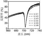
图13为6个由同一硅模板上复制的生物传感器的反射谱;Figure 13 is the reflectance spectra of 6 biosensors replicated on the same silicon template;
图14中(a)为不同凹槽深度的金纳米凹槽阵列的反射谱、(b)最佳槽深参数下的光谱;Among Fig. 14 (a) is the reflection spectrum of the gold nano groove array of different groove depths, (b) the spectrum under the optimal groove depth parameter;
图15为采用本发明一实施例中制备方法对镀金过程中出现金层非对称效应和厚度误差的规避示意图;Fig. 15 is a schematic diagram of avoiding the asymmetric effect and thickness error of the gold layer during the gold plating process by using the preparation method in an embodiment of the present invention;
图16为采用图1对应的生物传感器时滴加不同浓度的AFP抗原溶液时的反射谱;Figure 16 is the reflectance spectrum when the AFP antigen solution of different concentrations is dripped when using the biosensor corresponding to Figure 1;
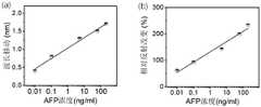
图17中(a)为图1对应的生物传感器波长移动和AFP浓度之间的关系曲线、(b)为图1对应的生物传感器相对反射率改变和AFP浓度之间的关系曲线;In Figure 17, (a) is the relationship curve between the wavelength shift of the biosensor corresponding to Figure 1 and the AFP concentration, and (b) is the relationship curve between the relative reflectance change of the biosensor corresponding to Figure 1 and the AFP concentration;
图18中(a)为图1对应的生物传感器在不同浓度丙三醇水溶液中的反射谱、(b)为图1对应的生物传感器的波长移动和不同浓度丙三醇水溶液的折射率的关系曲线;In Figure 18, (a) is the reflectance spectrum of the biosensor corresponding to Figure 1 in different concentrations of glycerin aqueous solution, and (b) is the relationship between the wavelength shift of the biosensor corresponding to Figure 1 and the refractive index of different concentrations of glycerin aqueous solution curve;
图19为不同工作波长的金属凹槽的反射谱;Figure 19 is the reflectance spectrum of metal grooves with different working wavelengths;
图20中(a)为金属凹槽一维阵列示意图、(b)为金属凹槽二维阵列示意图。In Fig. 20, (a) is a schematic diagram of a one-dimensional array of metal grooves, and (b) is a schematic diagram of a two-dimensional array of metal grooves.
100、生物传感器;101、介质层;102、金属层;1021、金属凹槽;103、衬底;200、模板;201、辅助凸起;300、掩膜材料。100. biosensor; 101. medium layer; 102. metal layer; 1021. metal groove; 103. substrate; 200. template; 201. auxiliary protrusion; 300. mask material.
具体实施方式detailed description
为使本发明的上述目的、特征和优点能够更加明显易懂,下面对本发明的具体实施方式做详细的说明。在下面的描述中阐述了很多具体细节以便于充分理解本发明。但是本发明能够以很多不同于在此描述的其它方式来实施,本领域技术人员可以在不违背本发明内涵的情况下做类似改进,因此本发明不受下面公开的具体实施例的限制。In order to make the above objects, features and advantages of the present invention more obvious and comprehensible, specific implementations of the present invention will be described in detail below. In the following description, numerous specific details are set forth in order to provide a thorough understanding of the present invention. However, the present invention can be implemented in many other ways different from those described here, and those skilled in the art can make similar improvements without departing from the connotation of the present invention, so the present invention is not limited by the specific embodiments disclosed below.
此外,术语“第一”、“第二”仅用于描述目的,而不能理解为指示或暗示相对重要性或者隐含指明所指示的技术特征的数量。由此,限定有“第一”、“第二”的特征可以明示或者隐含地包括至少一个该特征。在本发明的描述中,“多个”的含义是至少两个,例如两个,三个等,除非另有明确具体的限定。In addition, the terms "first" and "second" are used for descriptive purposes only, and cannot be interpreted as indicating or implying relative importance or implicitly specifying the quantity of indicated technical features. Thus, the features defined as "first" and "second" may explicitly or implicitly include at least one of these features. In the description of the present invention, "plurality" means at least two, such as two, three, etc., unless otherwise specifically defined.
在本发明中,除非另有明确的规定和限定,术语“安装”、“相连”、“连接”、“固定”等术语应做广义理解,例如,可以是固定连接,也可以是可拆卸连接,或成一体;可以是机械连接,也可以是电连接;可以是直接相连,也可以通过中间媒介间接相连,可以是两个元件内部的连通或两个元件的相互作用关系,除非另有明确的限定。对于本领域的普通技术人员而言,可以根据具体情况理解上述术语在本发明中的具体含义。In the present invention, unless otherwise clearly specified and limited, terms such as "installation", "connection", "connection" and "fixation" should be understood in a broad sense, for example, it can be a fixed connection or a detachable connection , or integrated; it may be mechanically connected or electrically connected; it may be directly connected or indirectly connected through an intermediary, and it may be the internal communication of two components or the interaction relationship between two components, unless otherwise specified limit. Those of ordinary skill in the art can understand the specific meanings of the above terms in the present invention according to specific situations.
除非另有定义,本文所使用的所有的技术和科学术语与属于本发明的技术领域的技术人员通常理解的含义相同。本文中在本发明的说明书中所使用的术语只是为了描述具体的实施例的目的,不是旨在于限制本发明。本文所使用的术语“和/或”包括一个或多个相关的所列项目的任意的和所有的组合。Unless otherwise defined, all technical and scientific terms used herein have the same meaning as commonly understood by one of ordinary skill in the technical field of the invention. The terms used herein in the description of the present invention are for the purpose of describing specific embodiments only, and are not intended to limit the present invention. As used herein, the term "and/or" includes any and all combinations of one or more of the associated listed items.
请参阅图1、图2、图8和图9,本发明一实施例提供了一种实现FP-WA耦合模式的生物传感器100。该生物传感器100包括介质层101和金属层102;介质层101具有多个介质凹槽,多个介质凹槽周期性等间距分布,介质凹槽在自其槽口到槽底的方向上的开口宽度逐渐减小;金属层102设在介质层101之上并对应各介质凹槽形成金属凹槽1021;Please refer to FIG. 1 , FIG. 2 , FIG. 8 and FIG. 9 , an embodiment of the present invention provides a
金属凹槽1021的周期满足式(1):The period of the

金属凹槽1021的深度、金属凹槽1021的槽口宽度以及金属凹槽1021的槽底宽度满足式(2):The depth of the

其中,
a代表金属凹槽的周期,h代表金属凹槽的深度,w0代表金属凹槽的槽口宽度,w1代表金属凹槽的槽底宽度,i代表WA模式的阶数,λWA代表WA模式的谐振波长,m代表FP模式的阶数,λWG代表FP模式的谐振波长,k代表FP模式的谐振波数,
在其中一个实施例中,金属凹槽的周期为600nm~1500nm,金属凹槽的深度为300nm~800nm,金属凹槽的槽口宽度为400nm~600nm,金属凹槽的槽底宽度为200nm~400nm。可以理解的是,金属凹槽的周期可以是但不限定为600nm、650nm、700nm、750nm、800nm、850nm、900nm、950nm、1000nm、1050nm、1100nm、1150nm、1200nm、1250nm、1300nm、1350nm、1400nm、1450nm或1500nm。金属凹槽的深度可以是但不限定为300nm、330nm、350nm、375nm、380nm、400nm、425nm、450nm、475nm、500nm、505nm、530nm、555nm、580nm、600nm、610nm、640nm、665nm、695nm、710nm、725nm、755nm、785nm或800nm。金属凹槽的槽口宽度可以是但不限定为400nm、420nm、440nm、450nm、460nm、470nm、480nm、490nm、500nm、510nm、520nm、530nm、540nm、550nm、560nm、570nm、580nm、590nm或600nm。金属凹槽的槽底宽度可以是但不限定为200nm、210nm、220nm、230nm、240nm、250nm、260nm、270nm、280nm、290nm、300nm、3100nm、320nm、330nm、340nm、350nm、360nm、370nm、380nm、390nm或400nm。In one of the embodiments, the period of the metal groove is 600nm-1500nm, the depth of the metal groove is 300nm-800nm, the width of the notch of the metal groove is 400nm-600nm, and the width of the bottom of the metal groove is 200nm-400nm . It can be understood that the period of the metal groove can be but not limited to 600nm, 650nm, 700nm, 750nm, 800nm, 850nm, 900nm, 950nm, 1000nm, 1050nm, 1100nm, 1150nm, 1200nm, 1250nm, 1300nm, 1350nm, 1400nm, 1450nm or 1500nm. The depth of the metal groove can be but not limited to 300nm, 330nm, 350nm, 375nm, 380nm, 400nm, 425nm, 450nm, 475nm, 500nm, 505nm, 530nm, 555nm, 580nm, 600nm, 610nm, 640nm, 665nm, 695nm, 710nm , 725nm, 755nm, 785nm or 800nm. The slot width of the metal groove can be but not limited to 400nm, 420nm, 440nm, 450nm, 460nm, 470nm, 480nm, 490nm, 500nm, 510nm, 520nm, 530nm, 540nm, 550nm, 560nm, 570nm, 580nm, 590nm or 600nm . The groove bottom width of the metal groove can be but not limited to 200nm, 210nm, 220nm, 230nm, 240nm, 250nm, 260nm, 270nm, 280nm, 290nm, 300nm, 3100nm, 320nm, 330nm, 340nm, 350nm, 360nm, 370nm, 380nm , 390nm or 400nm.
在一个具体的示例中,生物传感器的谐振线宽为3nm~9nm。比如,生物传感器的谐振线宽可以为3.1nm、3.2nm、3.3nm、3.4nm、3.5nm、3.6nm、3.7nm、3.8nm、3.9nm、4.0nm、4.1nm、4.2nm、4.3nm、4.4nm、4.5nm、4.6nm、4.7nm、4.8nm、4.9nm、5.0nm、5.1nm、5.2nm、5.3nm、5.4nm、5.5nm、5.6nm、5.7nm、5.8nm、5.9nm、6.0nm、6.1nm、6.2nm、6.3nm、6.4nm、6.5nm、6.6nm、6.7nm、6.8nm、6.9nm、7.0nm、7.1nm、7.2nm、7.3nm、7.4nm、7.5nm、7.6nm、7.7nm、7.8nm、7.9nm、8.0nm、8.1nm、8.2nm、8.3nm、8.4nm、8.5nm、8.6nm、8.7nm、8.8nm、8.9nm或9.0nm。In a specific example, the resonance linewidth of the biosensor is 3nm-9nm. For example, the resonance linewidth of the biosensor can be 3.1nm, 3.2nm, 3.3nm, 3.4nm, 3.5nm, 3.6nm, 3.7nm, 3.8nm, 3.9nm, 4.0nm, 4.1nm, 4.2nm, 4.3nm, 4.4nm nm, 4.5nm, 4.6nm, 4.7nm, 4.8nm, 4.9nm, 5.0nm, 5.1nm, 5.2nm, 5.3nm, 5.4nm, 5.5nm, 5.6nm, 5.7nm, 5.8nm, 5.9nm, 6.0nm, 6.1nm, 6.2nm, 6.3nm, 6.4nm, 6.5nm, 6.6nm, 6.7nm, 6.8nm, 6.9nm, 7.0nm, 7.1nm, 7.2nm, 7.3nm, 7.4nm, 7.5nm, 7.6nm, 7.7nm , 7.8nm, 7.9nm, 8.0nm, 8.1nm, 8.2nm, 8.3nm, 8.4nm, 8.5nm, 8.6nm, 8.7nm, 8.8nm, 8.9nm or 9.0nm.
在本实施例的生物传感器中,通过对结构进行设置,在介质层上形成多个周期性等间距分布的金属凹槽,每个金属凹槽相当于一个谐振器,在金属凹槽里面支持一种线宽较宽的法布里-泊罗腔模式(FP模式),同时,金属凹槽的周期性诱导了伍德异常(Wood’anomaly)模式(WA模式)。根据式(1)和式(2)中的结构参数和谐振波长的关系来对金属凹槽的周期、金属凹槽的深度、金属凹槽的槽口宽度以及金属凹槽的槽底宽度进行设定,使得FP模式和WA模式的波长互相靠近,得到一种极窄线宽和极深反射谷的耦合模式,即FP-WA耦合模式,进而得到了一种谐振峰线宽小、品质因子高的生物传感器。同时,本实施例中生物传感器结构简单,FP-WA耦合模式可以在垂直入射下激发,因此避免了基于斜入射激发的生物传感器所需的高精度角度调节组件,更加利于器件集成,便于转运和使用,能够有效促进生物检测由“集中化”向“分散化”转变。In the biosensor of this embodiment, by setting the structure, a plurality of metal grooves distributed periodically and equally spaced are formed on the dielectric layer, each metal groove is equivalent to a resonator, and a metal groove is supported in the metal groove. A wide linewidth Fabry-Perot cavity mode (FP mode), meanwhile, the periodicity of metal grooves induces Wood'anomaly (Wood'anomaly) mode (WA mode). According to the relationship between the structural parameters and the resonance wavelength in formula (1) and formula (2), the period of the metal groove, the depth of the metal groove, the width of the notch of the metal groove and the width of the bottom of the metal groove are set. fixed, so that the wavelengths of the FP mode and the WA mode are close to each other, and a coupling mode with an extremely narrow linewidth and a deep reflection valley is obtained, that is, the FP-WA coupling mode, and then a resonance peak with a small linewidth and a high quality factor is obtained. biosensors. At the same time, the structure of the biosensor in this embodiment is simple, and the FP-WA coupling mode can be excited under vertical incidence, thus avoiding the high-precision angle adjustment components required by the biosensor based on oblique incidence excitation, which is more conducive to device integration, and is convenient for transportation and Using it can effectively promote the transformation of biological detection from "centralization" to "decentralization".
可以理解的是,如图7所示,在实际设计中,可以在金属层102的部分区域形成金属凹槽1021。进一步地,可以使金属层102的面积大于介质层的具有凹槽的表面的面积。It can be understood that, as shown in FIG. 7 , in an actual design, a
还可以理解的是,金属层覆盖于介质层的表面以在各介质凹槽的表面对应形成金属凹槽,表示金属层将介质凹槽整体覆盖,使得金属凹槽覆盖在介质凹槽的表面。此时,介质凹槽的槽底、侧面以及相邻两个介质凹槽之间的连接面都被金属层覆盖。It can also be understood that the metal layer covers the surface of the dielectric layer to form metal grooves on the surface of each dielectric groove, which means that the metal layer covers the entire dielectric groove so that the metal groove covers the surface of the dielectric groove. At this time, the groove bottom and side surfaces of the dielectric groove and the connection surfaces between two adjacent dielectric grooves are all covered by the metal layer.
在对生物传感器进行设计时,发明人发现,在本实施例的生物传感器中,每个金属凹槽可以看一个谐振器,在金属凹槽中支持一种线宽较宽的FP模式(如图11中(a)所示),FP模式是一种局域模,具有较强的局域电场,也具有较大的辐射损耗,通过对金属凹槽的深度、金属凹槽的槽口宽度和金属凹槽的槽底宽度进行调节可以调整FP模式的谐振波长。同时,金属凹槽的周期性诱导了WA模式,WA是一种传播模,具有极低的辐射损耗和极窄的线宽(如图11中(b)所示),通过调整金属凹槽的周期可以调节WA模式的谐振波长。基于此,根据式(1)和式(2)中的结构参数和谐振波长的关系来对金属凹槽的周期、金属凹槽的深度、金属凹槽的槽口宽度以及金属凹槽的槽底宽度进行设定,使得FP模式和WA模式的波长互相靠近,得到一种极窄线宽和极深反射谷的耦合模式,此时可以达到一种临界耦合条件,使FP模式和WA模式的谐振波长靠近甚至相等,辐射衰减率等于内部衰减率,产生一种谐振峰线宽小、高品质因子、高光学反差以及强局域场的FP-WA耦合模式(如图11中(c)所示)。此处辐射衰减率表示的是体系的表面等离激元转化为自由空间光子的速率,而内部衰减率表示的是体系的表面等离激元在体系内部转化成热能的速率。When designing the biosensor, the inventor found that in the biosensor of this embodiment, each metal groove can see a resonator, and a kind of FP mode with a wider line width is supported in the metal groove (as shown in Fig. 11 (a)), the FP mode is a localized mode, which has a strong localized electric field and a large radiation loss. Through the depth of the metal groove, the width of the metal groove and the Adjusting the bottom width of the metal groove can adjust the resonant wavelength of the FP mode. At the same time, the periodicity of the metal groove induces the WA mode. WA is a propagating mode with extremely low radiation loss and extremely narrow line width (as shown in (b) in Fig. 11). By adjusting the The period can tune the resonant wavelength of the WA mode. Based on this, the period of the metal groove, the depth of the metal groove, the notch width of the metal groove and the groove bottom of the metal groove are determined according to the relationship between the structural parameters and the resonance wavelength in formula (1) and formula (2). The width is set so that the wavelengths of the FP mode and the WA mode are close to each other, and a coupling mode with an extremely narrow linewidth and an extremely deep reflection valley is obtained. At this time, a critical coupling condition can be achieved, so that the resonance of the FP mode and the WA mode The wavelengths are close to or even equal, and the radiation attenuation rate is equal to the internal attenuation rate, resulting in a FP-WA coupling mode with small resonant peak linewidth, high quality factor, high optical contrast, and strong local field (as shown in (c) in Figure 11 ). Here, the radiative decay rate represents the rate at which the surface plasmons of the system are converted into free space photons, while the internal decay rate represents the rate at which the surface plasmons of the system are converted into heat energy inside the system.
在一个具体的示例中,金属层的厚度为200nm~500nm。金属层厚度太小可能会存在光透过金属层进入介质层的风险,导致检测准确性降低,金属层厚度太大则会增加传感器的制造成本。可选地,金属层的厚度可以是但不限定为200nm、250nm、300nm、350nm、400nm、450nm或500nm。金属层的厚度优选为300nm。In a specific example, the thickness of the metal layer is 200nm˜500nm. If the thickness of the metal layer is too small, there may be a risk of light passing through the metal layer and entering the dielectric layer, resulting in a decrease in detection accuracy. If the thickness of the metal layer is too large, the manufacturing cost of the sensor will be increased. Optionally, the thickness of the metal layer may be, but not limited to, 200nm, 250nm, 300nm, 350nm, 400nm, 450nm or 500nm. The thickness of the metal layer is preferably 300 nm.
进一步地,金属层为稳定金属层。更进一步地,金属层为金层、铂层以及银层中至少一种。可以理解的是,金属层可以是稳定金属层的单层结构,也可以是不同的稳定金属层构成的叠层结构。比如,金属层可以是金层、铂层或银层的单层结构,也可以是金层、铂层以及银层中至少两种组成的叠层结构。Further, the metal layer is a stable metal layer. Furthermore, the metal layer is at least one of a gold layer, a platinum layer and a silver layer. It can be understood that the metal layer may be a single-layer structure of a stable metal layer, or may be a stacked structure composed of different stable metal layers. For example, the metal layer may be a single layer structure of gold layer, platinum layer or silver layer, or may be a stacked structure composed of at least two of gold layer, platinum layer and silver layer.
作为金属层的表面粗糙度的一个优选范围,金属层的表面粗糙度的均方根为0.2nm~1.9nm。此时金属层具有十分光滑的表面,可以有效减少金属层表面颗粒效应造成的散射损耗,进一步减小FP-WA耦合模式的谐振峰线宽。优选地,金属层的表面粗糙度的均方根不超过0.5nm,进一步优选地,金属层的表面粗糙度的均方根不超过0.36nm。可以理解的是,金属层的表面粗糙度的均方根为0.2nm~1.9nm,表示金层远离介质层的表面的粗糙度的均方根为0.2nm~1.9nm。通过将金属层的表面粗糙度的均方根设置为0.2nm~1.9nm,可以进一步提高生物传感器的品质因子。在一个具体的示例中,生物传感器的品质因子可达285。更具体地,金属层为金层时,金属层的表面粗糙度的均方根优选为0.2nm~0.8nm。金属层为银层时,金属层的表面粗糙度的均方根优选为0.4nm~1.5nm。As a preferable range of the surface roughness of the metal layer, the root mean square of the surface roughness of the metal layer is 0.2 nm to 1.9 nm. At this time, the metal layer has a very smooth surface, which can effectively reduce the scattering loss caused by the particle effect on the surface of the metal layer, and further reduce the resonant peak linewidth of the FP-WA coupling mode. Preferably, the root mean square of the surface roughness of the metal layer does not exceed 0.5 nm, further preferably, the root mean square of the surface roughness of the metal layer does not exceed 0.36 nm. It can be understood that the root mean square of the surface roughness of the metal layer is 0.2nm-1.9nm, which means that the root mean square roughness of the surface of the gold layer away from the dielectric layer is 0.2nm-1.9nm. By setting the root mean square of the surface roughness of the metal layer to 0.2nm˜1.9nm, the quality factor of the biosensor can be further improved. In one specific example, the quality factor of the biosensor can be up to 285. More specifically, when the metal layer is a gold layer, the root mean square of the surface roughness of the metal layer is preferably 0.2 nm to 0.8 nm. When the metal layer is a silver layer, the root mean square of the surface roughness of the metal layer is preferably 0.4 nm to 1.5 nm.
可以理解的是,介质层为热固化环氧树脂介质层或光固化环氧树脂介质层。进一步地,光固化环氧树脂介质层为紫外光固化环氧介质层。It can be understood that the medium layer is a heat-cured epoxy resin medium layer or a light-cured epoxy resin medium layer. Further, the light-cured epoxy resin medium layer is an ultraviolet light-cured epoxy medium layer.
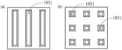
在一个具体的示例中,多个介质凹槽呈多行多列分布,各行相互平行,各列相互平行,且各行与各列相互垂直。具体地,介质凹槽的槽口为正方形,槽口宽度为正方形的边长。在另一个具体的示例中,介质凹槽的槽口为圆形,槽口宽度为圆形的直径。In a specific example, the plurality of dielectric grooves are distributed in multiple rows and columns, each row is parallel to each other, each column is parallel to each other, and each row and each column are perpendicular to each other. Specifically, the notch of the medium groove is a square, and the width of the notch is the side length of the square. In another specific example, the notch of the medium groove is a circle, and the width of the notch is the diameter of the circle.
在另一个具体的示例中,各行的介质凹槽相连通以形成宽度均匀的连通凹槽;或者,各列的介质凹槽相连通以形成宽度均匀的连通凹槽。此时金属凹槽的结构对应图1、图2、图8和图9所示。In another specific example, the dielectric grooves in each row are connected to form a communication groove with a uniform width; or, the dielectric grooves in each column are connected to form a communication groove with a uniform width. At this time, the structure of the metal groove corresponds to that shown in FIG. 1 , FIG. 2 , FIG. 8 and FIG. 9 .
请参阅图20,当多个介质凹槽呈多行多列分布,各行相互平行,各列相互平行,且各行与各列相互垂直时,能够形成金属凹槽的二维阵列分布(图20中(b)所示)。当各行的介质凹槽相连通;或者,各列的介质凹槽相连通时,能够形成金属凹槽的一维阵列分布(图20中(a)所示)。Please refer to Figure 20, when a plurality of dielectric grooves are distributed in multiple rows and columns, each row is parallel to each other, each column is parallel to each other, and when each row and each column are perpendicular to each other, a two-dimensional array distribution of metal grooves can be formed (in Figure 20 (b) shown). When the dielectric grooves of each row are connected; or, when the dielectric grooves of each column are connected, a one-dimensional array distribution of metal grooves can be formed (as shown in (a) in FIG. 20 ).
在一个具体的示例中,生物传感器100还包括衬底103,衬底103设于介质层101的远离金属层102的表面。可选地,衬底103为玻璃衬底。In a specific example, the
请参阅图3~图6,本发明还有一实施例提供了一种上述生物传感器的制备方法。该制备方法包括如下步骤:在模板200上形成周期性等间距分布的辅助凸起201;在模板的表面形成金属层102,金属层102对应各辅助凸起201形成金属凹槽1021;在金属层102之上形成介质层101;分离金属层102与模板。采用该制备方法能够使金属层与模板具有同样的光滑表面,能够有效提高金属层的光滑性,这样可以进一步降低谐振峰线宽、提高品质因子。同时采用上述制备方法能够有效避免金属层厚度变化和金属层不对称而影响生物传感器的光学响应等问题。优选地,模板为硅片。硅片具有更优的光滑性能,能够进一步提高金属层的光滑性。Please refer to FIG. 3 to FIG. 6 , another embodiment of the present invention provides a preparation method of the above-mentioned biosensor. The preparation method includes the following steps: forming
具体地,当本实施例中的方法制备生物传感器时,金属凹槽的光学响应主要由硅片和金属层之间的界面决定,当金属层厚度表现为如图15中(a)所示的对称、如图15中(b)所示的非对称或者如图15中(c)所示的厚度变薄时,硅片和金属层之间的界面是一致的,因此不会影响生物传感器的光学响应。Specifically, when the biosensor is prepared by the method in this example, the optical response of the metal groove is mainly determined by the interface between the silicon wafer and the metal layer, when the thickness of the metal layer is as shown in (a) in Figure 15 When symmetrical, asymmetrical as shown in Figure 15(b), or thinned as shown in Figure 15(c), the interface between the silicon wafer and the metal layer is consistent and thus does not affect the biosensor optical response.
进一步地,采用本实施例中的制备方法能够得到金属层的表面粗糙度的均方根为0.2nm~1.9nm的金属层,这样能够大大提高金属层的光滑性。进一步减小FP-WA耦合模式的谐振峰线宽。而传统的直接蒸镀或者溅射的金属膜表面的粗糙度的均方根大于2nm。比如,传统的直接蒸镀或者溅射的金膜表面的粗糙度的均方根大于2nm,传统的直接蒸镀或者溅射的银膜表面的粗糙度的均方根大于4nm。即本实施例中提供了一种能够有效降低金属层表面粗糙度均方根的金属层的制备方法,可以将其应用到低表面粗糙度金属层的制备中。Furthermore, the metal layer with a root mean square roughness of 0.2 nm to 1.9 nm can be obtained by using the preparation method in this embodiment, which can greatly improve the smoothness of the metal layer. Further reduce the resonant peak linewidth of the FP-WA coupling mode. However, the root-mean-square roughness of the surface of the traditional direct evaporation or sputtering metal film is greater than 2nm. For example, the root mean square roughness of the surface of the traditional directly evaporated or sputtered gold film is greater than 2 nm, and the root mean square roughness of the surface of the traditional directly evaporated or sputtered silver film is greater than 4 nm. That is, this embodiment provides a method for preparing a metal layer that can effectively reduce the root-mean-square surface roughness of the metal layer, which can be applied to the preparation of a metal layer with a low surface roughness.
在一个具体的示例中,在模板上形成周期性的辅助凸起201包括如下步骤:在模板表面覆盖掩膜材料;对掩膜材料进行曝光、显影处理,在模板表面形成与辅助凸起201相匹配的掩膜材料300,得到掩膜模板(掩膜模板如图3所示);对掩膜模板进行蚀刻处理,形成辅助凸起201;去除掩膜模板上的掩膜材料。In a specific example, forming the periodic
可以理解的是,掩膜材料可以是但不限定为聚甲基丙烯酸甲酯,在实际操作过程中,在硅模板的表面旋涂一层聚甲基丙烯酸甲酯薄膜。优选地,控制聚甲基丙烯酸甲酯薄膜的厚度为850nm~950nm,进一步优选为900nm。It can be understood that the mask material may be, but not limited to, polymethyl methacrylate. During actual operation, a layer of polymethyl methacrylate film is spin-coated on the surface of the silicon template. Preferably, the thickness of the polymethyl methacrylate film is controlled to be 850nm-950nm, more preferably 900nm.
覆盖掩膜材料之后采用曝光、显影对掩膜材料进行处理,得到图3所示的掩膜模板。对掩膜模板进行蚀刻处理,然后去除掩膜模板上剩余的掩膜材料,得到如图4所示的具有周期性辅助凸起201的模板。得到如图4所示的模板之后,在该模板上形成金属层,得到具有如图5所示的具有金属层的模板,然后再在具有金属层的模板上形成介质层,还可以继续在介质层表面形成衬底,进而得到具有如图6所示的结构。可以理解的是,曝光、显影、蚀刻可以选用标准的电子束光刻流程。在模板上形成金属层可以采用金属沉积的方式,优选地,控制金属层的厚度为200nm~500nm。在得到具有如图5所示的具有金属层的模板之后,分离金属层和模板,可以得到表面光滑且具有周期性凹槽的金属层。After the mask material is covered, the mask material is processed by exposure and development to obtain the mask template shown in FIG. 3 . The mask template is etched, and then the remaining mask material on the mask template is removed to obtain a template with periodic
进一步地,在金属层的表面形成介质层包括如下步骤:将热固化环氧树脂或热固化环氧树脂转移到金属层的表面,然后固化成型。更进一步地,固化成型之前在介质层表面覆盖衬底以促进介质层成型。可选地,衬底为玻璃。Further, forming the dielectric layer on the surface of the metal layer includes the following steps: transferring heat-cured epoxy resin or heat-cured epoxy resin to the surface of the metal layer, and then curing and molding. Furthermore, the substrate is covered on the surface of the dielectric layer before curing and molding to facilitate the molding of the dielectric layer. Optionally, the substrate is glass.
在一个具体的示例中,分离金属层与模板之后还包括如下步骤:对模板进行清洗处理。对模板进行清洗处理除去模板表面残余的介质层材料和金属层材料,可以实现模板的重复利用。具体地,对模板进行清洗处理包括如下步骤:对模板依次采用丙酮、碘/碘化钾混合溶液以及乙醇进行清洗处理。进一步地,碘/碘化钾混合溶液中碘、碘化钾以及水的质量比为3:(8~12):(135~145)。更进一步地,碘/碘化钾混合溶液中碘、碘化钾以及水的质量比为3:10:140。In a specific example, after separating the metal layer and the template, the following step is further included: cleaning the template. Cleaning the template to remove the residual dielectric layer material and metal layer material on the template surface can realize the reuse of the template. Specifically, cleaning the template includes the following steps: sequentially cleaning the template with acetone, iodine/potassium iodide mixed solution and ethanol. Further, the mass ratio of iodine, potassium iodide and water in the iodine/potassium iodide mixed solution is 3:(8-12):(135-145). Furthermore, the mass ratio of iodine, potassium iodide and water in the iodine/potassium iodide mixed solution is 3:10:140.
本发明还有一实施例提供了一种上述生物传感器在目标物感兴趣参数检测中的应用。具体地,该应用包括如下步骤:Still another embodiment of the present invention provides an application of the above-mentioned biosensor in detecting parameters of interest of a target. Specifically, the application includes the following steps:
将入射光沿垂直于金属凹槽的槽底的方向入射到金属层的表面,测量反射光的初始光学参数;The incident light is incident on the surface of the metal layer along the direction perpendicular to the groove bottom of the metal groove, and the initial optical parameters of the reflected light are measured;
在金属层表面分别滴加不同已知感兴趣参数的目标物溶液,并测量该溶液对应的反射光的标准光学参数;Dropping target solutions with different known parameters of interest on the surface of the metal layer, and measuring the standard optical parameters of the reflected light corresponding to the solution;
分别计算各不同已知感兴趣参数的溶液对应的标准光学参数与初始光学参数的差值,并基于该差值与对应的已知感兴趣参数获取光学参数随溶液感兴趣参数的变化关系;Calculating the difference between the standard optical parameter and the initial optical parameter corresponding to each solution with different known parameters of interest, and obtaining the relationship between the optical parameter and the parameter of interest in the solution based on the difference and the corresponding known parameter of interest;
在金属层表面滴加待测溶液,测试待测溶液对应的反射光的样品光学参数,并计算该样品光学参数与初始光学参数的差值,进而根据该差值与变化关系获取待测溶液的感兴趣参数。Drop the solution to be tested on the surface of the metal layer, test the sample optical parameters of the reflected light corresponding to the solution to be tested, and calculate the difference between the optical parameters of the sample and the initial optical parameters, and then obtain the solution to be tested according to the relationship between the difference and the change. parameters of interest.
进一步地,本发明还有一实施例提供了一种上述生物传感器以非疾病诊断目的在目标物感兴趣参数检测中的应用。具体地,该应用包括如下步骤:Furthermore, another embodiment of the present invention provides an application of the above-mentioned biosensor in the detection of parameters of interest of a target object for non-disease diagnosis purposes. Specifically, the application includes the following steps:
将入射光沿垂直于金属凹槽的槽底的方向入射到金属层的表面,测量反射光的初始光学参数;The incident light is incident on the surface of the metal layer along the direction perpendicular to the groove bottom of the metal groove, and the initial optical parameters of the reflected light are measured;
在金属层表面分别滴加不同已知感兴趣参数的目标物溶液,并测量该溶液对应的反射光的标准光学参数;Dropping target solutions with different known parameters of interest on the surface of the metal layer, and measuring the standard optical parameters of the reflected light corresponding to the solution;
分别计算各不同已知感兴趣参数的溶液对应的标准光学参数与初始光学参数的差值,并基于该差值与对应的已知感兴趣参数获取光学参数随溶液感兴趣参数的变化关系;Calculating the difference between the standard optical parameter and the initial optical parameter corresponding to each solution with different known parameters of interest, and obtaining the relationship between the optical parameter and the parameter of interest in the solution based on the difference and the corresponding known parameter of interest;
在金属层表面滴加待测溶液,测试待测溶液对应的反射光的样品光学参数,并计算该样品光学参数与初始光学参数的差值,进而根据该差值与变化关系获取待测溶液的感兴趣参数。Drop the solution to be tested on the surface of the metal layer, test the sample optical parameters of the reflected light corresponding to the solution to be tested, and calculate the difference between the optical parameters of the sample and the initial optical parameters, and then obtain the solution to be tested according to the relationship between the difference and the change. parameters of interest.
更具体地,目标物为盐、有机溶剂、抗原、抗体、DNA或RNA。感兴趣参数可以是浓度或折射率等能够通过光学参数反映的参数。More specifically, the target substance is a salt, an organic solvent, an antigen, an antibody, DNA or RNA. The parameter of interest may be a parameter that can be reflected by optical parameters such as concentration or refractive index.
在一个具体的示例中,上述生物传感器以非疾病诊断目的在生物体目标物浓度检测中的应用。具体地,该应用包括如下步骤:In a specific example, the above-mentioned biosensor is used in the detection of the concentration of biological targets for non-disease diagnosis purposes. Specifically, the application includes the following steps:
将入射光沿垂直于金属凹槽的槽底的方向入射到金属层的表面,测量反射光的初始光学参数;The incident light is incident on the surface of the metal layer along the direction perpendicular to the groove bottom of the metal groove, and the initial optical parameters of the reflected light are measured;
在金属层表面分别滴加不同已知浓度的生物体目标物溶液,并测量不同已知浓度的溶液对应的反射光的标准光学参数;Dropping biological target solutions of different known concentrations on the surface of the metal layer, and measuring the standard optical parameters of reflected light corresponding to the solutions of different known concentrations;
分别计算各不同已知浓度的溶液对应的标准光学参数与初始光学参数的差值,并基于该差值与对应的浓度获取光学参数随浓度的变化关系;Calculate the difference between the standard optical parameter and the initial optical parameter corresponding to each solution with different known concentrations, and obtain the relationship between the optical parameter and the concentration based on the difference and the corresponding concentration;
在金属层表面滴加待测溶液,测试待测溶液对应的反射光的光学参数,并计算该光学参数与初始光学参数的差值,进而根据该差值与变化曲线获取待测溶液的浓度。Drop the solution to be tested on the surface of the metal layer, test the optical parameters of the reflected light corresponding to the solution to be tested, and calculate the difference between the optical parameter and the initial optical parameter, and then obtain the concentration of the solution to be tested according to the difference and the change curve.
进一步地,生物体目标物为抗原、抗体、DNA或RNA。Furthermore, the biological target is an antigen, antibody, DNA or RNA.
可以理解的是,光学参数为谐振波长、反射率以及反射光强中的至少一种。其中,谐振波长为生物传感器的反射谷最低点所在的波长。反射率是指生物传感器反射光强和银镜(100%反射校准)反射光强之比。还可以理解的是,在计算光学参数之间的差值时,计算同一种光学参数之间的差值。It can be understood that the optical parameter is at least one of resonance wavelength, reflectivity and reflected light intensity. Wherein, the resonant wavelength is the wavelength at which the lowest reflection valley point of the biosensor is located. Reflectance is the ratio of the light intensity reflected by the biosensor to the light intensity reflected by the silver mirror (100% reflectance calibration). It can also be understood that when calculating the difference between optical parameters, the difference between the same optical parameters is calculated.
作为上述应用的一个具体例子,该应用为生物传感器在抗原浓度检测中的应用。具体地,该应用包括如下步骤:As a specific example of the above application, the application is the application of the biosensor in the detection of antigen concentration. Specifically, the application includes the following steps:
在生物传感的金属层表面滴加抗体溶液,并进行抗体固定处理;Drop the antibody solution on the surface of the biosensing metal layer, and perform antibody immobilization treatment;
将入射光沿垂直于金属凹槽的槽底的方向入射到金属层的表面,测量反射光的初始光学参数;The incident light is incident on the surface of the metal layer along the direction perpendicular to the groove bottom of the metal groove, and the initial optical parameters of the reflected light are measured;
在金属层表面分别滴加不同已知浓度的抗原溶液,使抗原和抗体进行特异性结合,并分别测量滴加各已知浓度的抗原溶液后对应的反射光的试验光学参数;Dropping antigen solutions of different known concentrations on the surface of the metal layer, so that the antigen and antibody can be specifically combined, and measuring the experimental optical parameters of the corresponding reflected light after dropping the antigen solutions of each known concentration;
分别计算各不同已知浓度的抗原溶液对应的试验光学参数与初始光学参数的差值,并基于该差值与对应的抗原溶液的浓度获取光学参数差值随抗原溶液溶度的变化曲线;Calculate the difference between the test optical parameters corresponding to the antigen solutions of different known concentrations and the initial optical parameters, and obtain a curve of the difference between the optical parameters and the solubility of the antigen solution based on the difference and the concentration of the corresponding antigen solution;
在金属层表面滴加待测抗原溶液,测试待测抗原溶液对应的反射光的光学参数,并计算该光学参数与所述初始光学参数的差值,进而根据该差值与所述变化曲线获取待测抗原溶液的抗原浓度。Add the antigen solution to be tested dropwise on the surface of the metal layer, test the optical parameters of the reflected light corresponding to the antigen solution to be tested, and calculate the difference between the optical parameter and the initial optical parameter, and then obtain according to the difference and the change curve The antigen concentration of the antigen solution to be tested.
在一个具体的示例中,抗体固定包括如下步骤:滴加抗体溶液之后在37℃下孵化,然后依次用磷酸盐缓冲液和去离子水清洗3次,并用氮气吹干。使抗原和抗体进行特异性结合包括如下步骤:滴加抗原溶液之后在37℃下孵化,然后依次用磷酸盐缓冲液和去离子水清洗3次,并用氮气吹干。In a specific example, the antibody immobilization includes the following steps: after adding the antibody solution dropwise, incubating at 37° C., then washing with phosphate buffer saline and deionized water for 3 times, and drying with nitrogen. The specific binding of antigen and antibody includes the following steps: after adding the antigen solution dropwise, incubate at 37°C, then wash with phosphate buffer saline and deionized water for 3 times, and blow dry with nitrogen.
在另一个具体的示例中,在生物传感的金属层表面滴加抗体溶液之前还包括如下步骤:对金属层的表面进行羧基化处理,然后进行羧基活化处理。具体地,羧基化处理包括如下步骤:将金属层与巯基丙酸的磷酸盐缓冲液溶液接触,然后依次用磷酸盐缓冲液和去离子水清洗3次,并用氮气吹干。羧基活化处理包括如下步骤将金属层与1-(3-二甲氨基丙基)-3-乙基碳二亚胺盐酸盐(EDC)和N-羟基琥珀酰亚胺(NHS)的混合溶液接触,然后依次用磷酸盐缓冲液和去离子水清洗3次,并用氮气吹干。EDC与NHS的摩尔比为4:1。In another specific example, before dripping the antibody solution on the surface of the biosensing metal layer, the following steps are further included: performing carboxylation treatment on the surface of the metal layer, and then performing carboxyl activation treatment. Specifically, the carboxylation treatment included the following steps: contacting the metal layer with a phosphate buffer solution of mercaptopropionic acid, followed by washing with phosphate buffer and deionized water for 3 times, and drying with nitrogen. The carboxyl group activation treatment includes the following steps to mix the metal layer with a mixed solution of 1-(3-dimethylaminopropyl)-3-ethylcarbodiimide hydrochloride (EDC) and N-hydroxysuccinimide (NHS) contact, then washed three times with phosphate buffered saline and deionized water, and blown dry with nitrogen. The molar ratio of EDC to NHS is 4:1.
可以理解的是,对金属层的表面进行羧基化处理之前还包括如下步骤:对金属层的表面进行亲水化处理。可选地,亲水化处理包括对金属层进行等离子蚀刻的步骤。It can be understood that, before performing the carboxylation treatment on the surface of the metal layer, the following step is also included: performing hydrophilic treatment on the surface of the metal layer. Optionally, the hydrophilization treatment includes the step of performing plasma etching on the metal layer.
可以理解的是,将入射光垂直照射到金属层的表面之前还包括如下步骤:对进行抗体固定处理之后的金属层的表面进行自由羧基封闭处理。具体地,自由羧基封闭处理包括如下步骤:将金属层与牛血清蛋白(BSA)溶液接触,然后依次用磷酸盐缓冲液和去离子水清洗3次,并用氮气吹干。It can be understood that before the incident light is vertically irradiated onto the surface of the metal layer, the following step is also included: performing free carboxyl group blocking treatment on the surface of the metal layer after antibody immobilization treatment. Specifically, the free carboxyl group blocking treatment includes the following steps: contact the metal layer with bovine serum albumin (BSA) solution, then wash with phosphate buffer saline and deionized water for 3 times, and blow dry with nitrogen.
本发明还有一实施例提供了一种上述生物传感器在测量溶液折射率的应用。具体地,该应用包括如下步骤:Still another embodiment of the present invention provides an application of the above-mentioned biosensor in measuring the refractive index of a solution. Specifically, the application includes the following steps:
将入射光沿垂直于金属凹槽的槽底的方向入射到金属层的表面,测量反射光的初始光学参数;The incident light is incident on the surface of the metal layer along the direction perpendicular to the groove bottom of the metal groove, and the initial optical parameters of the reflected light are measured;
在金属层表面分别滴加不同已知折射率的溶液,并测量不同已知折射率溶液对应的反射光的标准光学参数;Dropping solutions with different known refractive indices on the surface of the metal layer respectively, and measuring the standard optical parameters of the reflected light corresponding to the solutions with different known refractive indices;
分别计算各不同已知折射率溶液对应的标准光学参数与初始光学参数的差值,并基于该差值与对应的折射率获取光学参数随折射率的变化关系;Calculate the difference between the standard optical parameters and the initial optical parameters corresponding to the solutions with different known refractive indices, and obtain the relationship between the optical parameters and the refractive index based on the difference and the corresponding refractive index;
在金属层表面滴加待测溶液,测试待测溶液对应的反射光的光学参数,并计算该光学参数与初始光学参数的差值,进而根据该差值与变化关系获取待测溶液的折射率。Drop the solution to be tested on the surface of the metal layer, test the optical parameters of the reflected light corresponding to the solution to be tested, and calculate the difference between the optical parameter and the initial optical parameter, and then obtain the refractive index of the solution to be tested according to the relationship between the difference and the change .
优选地,多个介质凹槽呈多行多列分布,各行相互平行,各列相互平行,且各行与各列相互垂直;入射光的偏振方向与行方向垂直,或者入射光的偏振方向与列方向垂直。比如,当金属凹槽为如图20中(b)所示的二维阵列分布时,入射光的偏振方向与行方向垂直,或者入射光的偏振方向与列方向垂直。Preferably, the plurality of dielectric grooves are distributed in multiple rows and columns, each row is parallel to each other, each column is parallel to each other, and each row and each column are perpendicular to each other; the polarization direction of the incident light is perpendicular to the row direction, or the polarization direction of the incident light is perpendicular to the column Direction is vertical. For example, when the metal grooves are distributed in a two-dimensional array as shown in (b) in FIG. 20 , the polarization direction of the incident light is perpendicular to the row direction, or the polarization direction of the incident light is perpendicular to the column direction.
进一步地,各行的介质凹槽相连通以形成宽度均匀的连通凹槽;或者,各列的介质凹槽相连通以形成宽度均匀的连通凹槽;入射光的偏振方向与连通凹槽的延伸方向垂直。比如,当金属凹槽为如图20中(a)所示的一维阵列分布时,入射光的偏振方向与金属凹槽的延伸方向垂直。Further, the dielectric grooves of each row are connected to form a connected groove with a uniform width; or, the dielectric grooves of each column are connected to form a connected groove with a uniform width; the polarization direction of the incident light and the extending direction of the connected groove vertical. For example, when the metal grooves are distributed in a one-dimensional array as shown in (a) of FIG. 20 , the polarization direction of the incident light is perpendicular to the extending direction of the metal grooves.
以下为具体实施例。The following are specific examples.
实施例1Example 1
本实施例中生物传感器的金属凹槽为如图20中(a)所示的一维阵列分布。The metal grooves of the biosensor in this embodiment are distributed in a one-dimensional array as shown in (a) of FIG. 20 .
本实施例中生物传感器的制备方法包括如下步骤:The preparation method of the biosensor in this embodiment includes the following steps:
S101:在硅片上旋涂一层聚甲基丙烯酸甲酯薄膜。控制聚甲基丙烯酸甲酯薄膜的厚度为900nm。S101: spin coating a layer of polymethyl methacrylate film on the silicon wafer. Control the thickness of the polymethyl methacrylate film to 900nm.
S102:对聚甲基丙烯酸甲酯薄膜进行电子束曝光和显影,使得聚甲基丙烯酸甲酯薄膜具有光栅结构,得到掩膜硅片。其中,光栅周期是700nm,光栅条宽度是350nm。S102: Electron beam exposure and development are performed on the polymethyl methacrylate film, so that the polymethyl methacrylate film has a grating structure, and a masked silicon wafer is obtained. Wherein, the period of the grating is 700nm, and the width of the grating bars is 350nm.
S103:以聚甲基丙烯酸甲酯光栅结构作为掩模,对掩膜硅片进行反应离子束蚀刻,在硅片上形成辅助凸起,相邻的两个辅助凸起之间表现为凹槽结构,其中,凹槽的槽口宽度和槽底宽度分别为450nm和260nm,凹槽深度为350nm,阵列周期为700nm。S103: Using the polymethyl methacrylate grating structure as a mask, perform reactive ion beam etching on the masked silicon wafer to form auxiliary protrusions on the silicon wafer, and the gap between two adjacent auxiliary protrusions is a groove structure , wherein, the slot width and bottom width of the groove are 450nm and 260nm respectively, the groove depth is 350nm, and the array period is 700nm.
S104:用氧等离子蚀刻S103中得到的硅片,清除掉残余的聚甲基丙烯酸甲酯,形成具有辅助凸起的硅模板。S104: Etching the silicon wafer obtained in S103 with oxygen plasma to remove residual polymethyl methacrylate to form a silicon template with auxiliary bumps.
S105:利用磁控溅射仪在S104得到的硅模板上沉积垂直厚度为200nm的金,得到金层。其中,溅射电流为35mA,时间为500s。S105: Deposit gold with a vertical thickness of 200 nm on the silicon template obtained in S104 by using a magnetron sputtering apparatus to obtain a gold layer. Wherein, the sputtering current is 35mA, and the time is 500s.
S106:在金层上滴液态的紫外固化环氧树脂(型号为NOA61,Norland公司),用干净的载玻片盖在环氧树脂上,并向下压紧,使得载玻片和硅片之间的环氧树脂层厚度均匀,并覆盖满整个金层区域。所用载玻片的尺寸大于硅模板的尺寸。然后,用紫外灯从载玻片一端照射环氧树脂,使其固化。紫外灯的功率和固化时间分别为48W和20分钟。S106: Drop liquid UV-curable epoxy resin (model NOA61, Norland Company) on the gold layer, cover the epoxy resin with a clean glass slide, and press it down so that the gap between the glass slide and the silicon wafer is The epoxy resin layer between them has a uniform thickness and covers the entire gold layer area. The size of the slide used is larger than that of the silicon template. The epoxy is then cured by shining a UV light from one end of the slide. The power and curing time of the UV lamp were 48W and 20 minutes, respectively.
S107:用干净的小刀划开金层和硅模板的界面,使两者分离,形成金层表面光滑、具有周期性金凹槽、金凹槽呈一维阵列分布的生物传感器。该周期性金凹槽的结构参数为:周期为700nm,槽深为350nm,槽口宽度为440nm,槽底宽度为250nm,金层垂直厚度为200nm。该金层的原子力显微镜图如图10所示,由图10可知,金层的表面粗糙度的均方根为0.36nm,表明该方法能够得到超光滑的金凹槽。S107: Cut the interface between the gold layer and the silicon template with a clean knife to separate the two, forming a biosensor with a smooth surface of the gold layer, periodic gold grooves, and a one-dimensional array of gold grooves. The structural parameters of the periodic gold groove are: the period is 700nm, the groove depth is 350nm, the groove width is 440nm, the groove bottom width is 250nm, and the vertical thickness of the gold layer is 200nm. The atomic force microscope image of the gold layer is shown in FIG. 10 . It can be seen from FIG. 10 that the root mean square of the surface roughness of the gold layer is 0.36 nm, indicating that this method can obtain ultra-smooth gold grooves.
S108:依次用丙酮、乙醇和碘/碘化钾水溶液去除分离之后的硅模板上残余的环氧树脂和金,得到再生的硅模板。其中碘/碘化钾水溶液的配比为碘:碘化钾:去离子水=3:10:140。S108: Using acetone, ethanol and iodine/potassium iodide aqueous solution to remove residual epoxy resin and gold on the separated silicon template in sequence to obtain a regenerated silicon template. The ratio of iodine/potassium iodide aqueous solution is iodine: potassium iodide: deionized water=3:10:140.
本实施例中生物传感器具有很窄的谐振线宽,谐振线宽仅为4.7nm,具有优异的传感性能。The biosensor in this embodiment has a very narrow resonance linewidth, which is only 4.7nm, and has excellent sensing performance.
作为本实施例中生物传感器的一种性能验证,在本实施例中,固定w0=440nm,w1=250nm,a=700nm,εd=1(空气),εm取自Johnson-Christy的金介电常数的实验数据,根据式(2),画出不同阶数的FP模式的谐振波长和金凹槽深度的关系曲线,如图14中(a)中的虚线所示。根据式(1),画出WA模式的谐振波长和金凹槽深度的关系曲线,如图14中(a)中的点划线所示。利用有限时域差分法计算出不同金凹槽深度的金层的反射谱扫描图,如图14中(a)中的背景灰度图所示,其中,不同灰度代表不同的反射率。寻找图14中(a)中两种模式色散曲线的交点,发现交点处周期性金凹槽的谐振模式的色散曲线发生反常弯曲,出现线宽极窄的反射谷。具体地,在凹槽深度为h=350nm时,如图14中(b)所示,反射谷的强度降到0,说明达到临界耦合条件,也就是系统的辐射衰减率等于其内部衰减率。在该凹槽深度值下,极窄的谐振线宽和极大的谐振强度(即反射谷的深度,定义为谐振处光强的极大值和极小值之差)同时达到,因此是十分理想的结构参数。As a performance verification of the biosensor in this example, in this example, fix w0 =440nm, w1 =250nm, a=700nm, εd =1 (air), εm is taken from Johnson-Christy's According to the experimental data of gold permittivity, according to formula (2), draw the relationship curve between the resonant wavelength of FP modes of different orders and the depth of the gold groove, as shown by the dotted line in (a) in Figure 14. According to formula (1), draw the relationship curve between the resonant wavelength of the WA mode and the depth of the gold groove, as shown by the dotted line in (a) in FIG. 14 . The reflection spectrum scanning diagram of the gold layer with different gold groove depths is calculated by using the finite time domain difference method, as shown in the background grayscale image in (a) of Figure 14, where different grayscales represent different reflectivities. Looking for the intersection of the dispersion curves of the two modes in (a) in Figure 14, it is found that the dispersion curve of the resonance mode of the periodic gold groove at the intersection is abnormally bent, and a reflection valley with extremely narrow line width appears. Specifically, when the depth of the groove is h=350nm, as shown in (b) of Figure 14, the intensity of the reflection valley drops to 0, indicating that the critical coupling condition is reached, that is, the radiation attenuation rate of the system is equal to its internal attenuation rate. Under this groove depth value, the extremely narrow resonance linewidth and the extremely large resonance intensity (that is, the depth of the reflection valley, defined as the difference between the maximum value and the minimum value of the light intensity at the resonance) are achieved at the same time, so it is very Ideal structural parameters.
本实施例中生物传感器在抗原浓度检测中的应用包括如下步骤:The application of the biosensor in the detection of antigen concentration in this embodiment includes the following steps:
S201:对金层的表面进行亲水化处理:将S107中得到的生物传感器用氧等离子体刻蚀30秒,功率为200W。S201: Hydrophilicizing the surface of the gold layer: etching the biosensor obtained in S107 with oxygen plasma for 30 seconds with a power of 200W.
S202:对金层的表面进行羧基化处理:在室温下,将S201处理后的生物传感器浸泡在10mM的巯基丙酸的磷酸盐缓冲液中12小时,然后依次用磷酸盐缓冲液和去离子水清洗3次,并用氮气吹干。S202: Carboxylation treatment on the surface of the gold layer: at room temperature, soak the biosensor after S201 treatment in 10mM mercaptopropionic acid phosphate buffer for 12 hours, and then sequentially wash with phosphate buffer and
S203:对金层的表面进行羧基活化处理:在室温下,将S202处理后的生物传感器在400mM的1-(3-二甲氨基丙基)-3-乙基碳二亚胺盐酸盐(EDC)和100mM的N-羟基琥珀酰亚胺(NHS)混合水溶液中浸泡2小时,然后依次用磷酸盐缓冲液和去离子水清洗3次,并用氮气吹干。S203: Carboxyl activation treatment is carried out on the surface of the gold layer: at room temperature, the biosensor after S202 treatment is dissolved in 400 mM 1-(3-dimethylaminopropyl)-3-ethylcarbodiimide hydrochloride ( EDC) and 100 mM N-hydroxysuccinimide (NHS) mixed aqueous solution for 2 hours, then washed with phosphate buffer saline and deionized water for 3 times, and dried with nitrogen.
S204:在生物传感的金属层表面滴加抗体溶液并进行抗体固定:在S203处理后的生物传感器的金层表面滴加100μg/ml甲胎蛋白(AFP)抗体溶液,在37℃培养箱中孵化1小时,然后依次用磷酸盐缓冲液和去离子水清洗3次,并用氮气吹干。S204: Add antibody solution dropwise on the surface of the metal layer of the biosensing and carry out antibody immobilization: drop 100 μg/ml alpha-fetoprotein (AFP) antibody solution on the surface of the gold layer of the biosensor treated in S203, in a 37°C incubator Incubate for 1 hour, then wash with phosphate buffered saline and deionized water three times sequentially, and blow dry with nitrogen gas.
S205:将S204处理后的生物传感器在牛血清蛋白(BSA)溶液中浸泡40分钟,然后依次用磷酸盐缓冲液和去离子水清洗3次,并用氮气吹干。S205: Soak the biosensor treated in S204 in a bovine serum albumin (BSA) solution for 40 minutes, then wash it with phosphate buffer saline and deionized water for 3 times, and dry it with nitrogen.
S206:采用微区光学测量系统将入射光沿垂直于金凹槽的槽底的方向入射到金属层的表面,且入射光的偏振方向与金凹槽的延伸方向垂直,记录下此时生物传感器的反射谱,如图16中(a)~(e)中的实线所示。S206: Using the micro-area optical measurement system, the incident light is incident on the surface of the metal layer along the direction perpendicular to the groove bottom of the gold groove, and the polarization direction of the incident light is perpendicular to the extension direction of the gold groove, and the biosensor at this time is recorded The reflectance spectrum of , as shown by the solid lines in (a) to (e) in Figure 16.
S207:取浓度分别为0.01ng/ml、0.1ng/ml、5ng/ml、60ng/ml和200ng/ml的甲胎蛋白(AFP)抗原溶液分别滴在5个结构参数相同的生物传感器上,在37℃培养箱中孵化1小时,然后依次用磷酸盐缓冲液和去离子水清洗3次,并用氮气吹干。S207: Take alpha-fetoprotein (AFP) antigen solutions with concentrations of 0.01ng/ml, 0.1ng/ml, 5ng/ml, 60ng/ml and 200ng/ml respectively and drop them on five biosensors with the same structural parameters. Incubate in a 37°C incubator for 1 hour, then wash with phosphate buffered saline and deionized water three times, and blow dry with nitrogen.
S208:采用微区光学测量系统将入射光垂直照射到S207处理后的生物传感器的金层上,入射光的入射方向与金层槽底垂直,入射光的偏振方向与入射方向垂直,记录下此时生物传感器的反射谱,如图16中(a)~(e)中的虚线所示。S208: Use the micro-area optical measurement system to vertically irradiate the incident light onto the gold layer of the biosensor processed in S207, the incident direction of the incident light is perpendicular to the groove bottom of the gold layer, the polarization direction of the incident light is perpendicular to the incident direction, and record this The reflectance spectrum of the biosensor at time is shown by the dotted lines in (a)-(e) in FIG. 16 .
S209:对比加AFP抗原前后的光谱,整理出传感器的谐振波长移动随AFP抗原浓度的变化曲线,如图17中(a)所示。同时,整理出波长为704.645nm处传感器的相对反射率改变随AFP抗原浓度的变化曲线,如图17中(b)所示。由图16和图17可知,生物传感器对AFP抗原的检测限为0.01ng/ml,线性范围为0.01ng/ml-200ng/ml。基于图17中(a)和(b)中的变化曲线,可以确定在线性范围内相同结构参数的生物传感器的谐振波长移动或相对反射率改变所对应的抗原溶液浓度。S209: Comparing the spectra before and after adding the AFP antigen, sorting out the change curve of the resonance wavelength shift of the sensor with the concentration of the AFP antigen, as shown in (a) in FIG. 17 . At the same time, the relative reflectance change curve of the sensor at the wavelength of 704.645nm with the AFP antigen concentration was sorted out, as shown in (b) in FIG. 17 . It can be seen from Figure 16 and Figure 17 that the detection limit of the biosensor for AFP antigen is 0.01ng/ml, and the linear range is 0.01ng/ml-200ng/ml. Based on the change curves in (a) and (b) in Figure 17, the concentration of the antigen solution corresponding to the shift of resonance wavelength or the change of relative reflectance of biosensors with the same structural parameters in the linear range can be determined.
实施例2Example 2
本实施例中验证了实施例1中制备方法过程中硅模板的重复利用性。重复实施例1中S105~S108,得到另外5个由同一硅模板制备的生物传感器,分别记为复制1(实施例1中的生物传感器)、复制2、复制3、复制4、复制5和复制6。分别用显微光谱仪测量6个生物传感器的反射谱,结果如图13所示。由图13可知,6个传感器具有几乎相同的光谱,其谐振波长的标准误差仅0.06nm,其波长为702.5nm处的反射光强的标准误差仅为0.54%,说明实施例1中的制备方法得到的生物传感器具有很好的光学响应一致性。In this example, the reusability of the silicon template during the preparation method in Example 1 is verified. Repeat S105~S108 in Example 1 to obtain another 5 biosensors prepared by the same silicon template, which are respectively recorded as copy 1 (biosensor in Example 1),
实施例3Example 3
本实施例中生物传感器的金属凹槽为如图20中(a)所示的一维阵列分布。本实施例中周期性金凹槽的结构参数为:周期为700nm,槽深为350nm,槽口宽度为450nm,槽底宽度为260nm,金层垂直厚度为300nm。The metal grooves of the biosensor in this embodiment are distributed in a one-dimensional array as shown in (a) of FIG. 20 . The structural parameters of the periodic gold grooves in this embodiment are: the period is 700nm, the groove depth is 350nm, the groove width is 450nm, the groove bottom width is 260nm, and the vertical thickness of the gold layer is 300nm.
请参阅图12,本实施例中生物传感器的耦合模式下的半高全宽值仅为2nm,其中半高全宽值的定义为反射谷最高点与最低点光强之和的一半处对应的谱线宽度。Please refer to FIG. 12 , the full width at half maximum of the biosensor in the coupling mode in this embodiment is only 2nm, where the full width at half maximum is defined as the spectral line width corresponding to half of the sum of the light intensity at the highest point and the lowest point of the reflection valley.
本实施例测量丙三醇的折射率的方法包括如下步骤:The method for measuring the refractive index of glycerol in the present embodiment may further comprise the steps:
S301:配置浓度为0%、10%、20%、30%、40%、50%和60%的丙三醇水溶液,其对应的折射率为1.33303、1.34481、1.35749、1.3707、1.38413、1.39809和1.41299。S301: Prepare glycerol aqueous solutions with concentrations of 0%, 10%, 20%, 30%, 40%, 50% and 60%, and the corresponding refractive indices are 1.33303, 1.34481, 1.35749, 1.3707, 1.38413, 1.39809 and 1.41299 .
S302:将入射光沿垂直于金凹槽的槽底的方向入射到金属层的表面,且入射光的偏振方向与金凹槽的延伸方向垂直,测量反射光的初始谐振波长。S302: Incident light is incident on the surface of the metal layer along a direction perpendicular to the groove bottom of the gold groove, and the polarization direction of the incident light is perpendicular to the extension direction of the gold groove, and the initial resonance wavelength of the reflected light is measured.
S303:在金属层表面分别滴加S301中不同浓度的丙三醇水溶液,并测量对应的反射光的谐振波长。可以理解的是,在每次测量之后,用去离子水清洗传感器。S303: Dropping glycerol aqueous solutions with different concentrations in S301 respectively on the surface of the metal layer, and measuring the corresponding resonant wavelength of reflected light. It is understood that after each measurement, the sensor was rinsed with deionized water.
S304:分别计算各不同折射率溶液对应的反射光的谐振波长与初始谐振波长的差值,并基于该差值与对应的折射率获取谐振波长差值与折射率的变化曲线,如图18中(b)所示。S304: Calculate the difference between the resonance wavelength of the reflected light corresponding to each solution with different refractive index and the initial resonance wavelength, and obtain the change curve of the resonance wavelength difference and the refractive index based on the difference and the corresponding refractive index, as shown in Figure 18 (b) shown.
S305:在金属层表面滴加待测溶液,测试待测溶液对应的反射光的谐振波长,并计算该谐振波长与初始谐振波长的差值,进而根据该差值与图18中(b)所示的变化曲线获取待测溶液的折射率。在S303中还可以测量得到不同浓度的丙三醇水溶液情况下,反射光的反射率和谐振波长的关系,如图18中(a)所示。结合图18中(a)和(b),可以计算得出生物传感器具有681nm/RIU的灵敏度(S)和高达285的波长品质因子(FOMλ)。其中S=Δλ/Δn,Δλ为波长的改变量,Δn为折射率的改变量;FOMλ=S/FWHM,FWHM为谐振的半高全宽。S305: Drop the solution to be tested on the surface of the metal layer, test the resonant wavelength of the reflected light corresponding to the solution to be tested, and calculate the difference between the resonant wavelength and the initial resonant wavelength, and then calculate the difference between the resonant wavelength and the initial resonant wavelength according to the difference between the difference and that shown in (b) in Figure 18 Obtain the refractive index of the solution to be tested using the change curve shown. In S303, the relationship between the reflectance of reflected light and the resonance wavelength can also be measured under the condition of different concentrations of glycerol aqueous solution, as shown in (a) in FIG. 18 . Combining (a) and (b) in Figure 18, it can be calculated that the biosensor has a sensitivity (S) of 681 nm/RIU and a wavelength figure of merit (FOMλ ) as high as 285. Wherein S=Δλ/Δn, Δλ is the change of wavelength, Δn is the change of refractive index; FOMλ =S/FWHM, FWHM is the full width at half maximum of resonance.
实施例4Example 4
本实施例中对不同工作波长下的优选金凹槽尺寸进行了设计。本实施例中生物传感器的金属凹槽为如图20中(a)所示的一维阵列分布。In this embodiment, the optimal size of the gold groove at different working wavelengths is designed. The metal grooves of the biosensor in this embodiment are distributed in a one-dimensional array as shown in (a) of FIG. 20 .
S401:固定金凹槽的周期为600nm,槽口宽度和槽底宽度分别为420nm和220nm,根据式(1)确定其一阶WA的谐振波长为600nm。再根据式(2)估计二阶FP模式的谐振波长在600nm附近的槽深范围为200-400nm。利用时域有限差分法模拟不同槽深(200-400nm)的金凹槽的反射谱,从中搜寻线宽最窄、反射谷最深的FP-WA耦合模式,如图19中的#1所示。S401: The period of the fixed gold groove is 600nm, the groove width and groove bottom width are 420nm and 220nm respectively, and the resonance wavelength of the first-order WA is determined to be 600nm according to formula (1). Then according to formula (2), it is estimated that the resonant wavelength of the second-order FP mode is in the range of 200-400 nm in the groove depth near 600 nm. The reflection spectra of gold grooves with different groove depths (200-400nm) were simulated by the finite difference time domain method, and the FP-WA coupling mode with the narrowest line width and deepest reflection valley was searched, as shown in #1 in Figure 19.
S402:重复S401,分别固定金凹槽的周期(从600nm到1500nm),然后利用时域有限差分法分别扫描不同周期所对应的槽深范围内的反射谱,从中搜寻线宽最窄的FP-WA耦合模式。最终得到若干个不同工作波长的金纳米槽阵列的最佳结构参数,如下表所示。不同工作波长的金凹槽的反射谱如图19所示。S402: Repeat S401, respectively fix the period of the gold groove (from 600nm to 1500nm), and then use the finite difference time domain method to scan the reflection spectra in the groove depth corresponding to different periods, and search for the FP- WA coupling mode. Finally, the optimal structural parameters of several gold nanogroove arrays with different working wavelengths are obtained, as shown in the table below. The reflectance spectra of the gold grooves at different working wavelengths are shown in Fig. 19 .


以上所述实施例的各技术特征可以进行任意的组合,为使描述简洁,未对上述实施例中的各个技术特征所有可能的组合都进行描述,然而,只要这些技术特征的组合不存在矛盾,都应当认为是本说明书记载的范围。The technical features of the above-mentioned embodiments can be combined arbitrarily. To make the description concise, all possible combinations of the technical features in the above-mentioned embodiments are not described. However, as long as there is no contradiction in the combination of these technical features, should be considered as within the scope of this specification.
以上所述实施例仅表达了本发明的几种实施方式,其描述较为具体和详细,但并不能因此而理解为对发明专利范围的限制。应当指出的是,对于本领域的普通技术人员来说,在不脱离本发明构思的前提下,还可以做出若干变形和改进,这些都属于本发明的保护范围。因此,本发明专利的保护范围应以所附权利要求为准,说明书及附图可以用于解释权利要求的内容。The above-mentioned embodiments only express several implementation modes of the present invention, and the descriptions thereof are relatively specific and detailed, but should not be construed as limiting the patent scope of the invention. It should be pointed out that those skilled in the art can make several modifications and improvements without departing from the concept of the present invention, and these all belong to the protection scope of the present invention. Therefore, the protection scope of the patent for the present invention should be determined by the appended claims, and the description and drawings can be used to explain the contents of the claims.
Claims (10)
Translated fromChinese


Priority Applications (3)
| Application Number | Priority Date | Filing Date | Title |
|---|---|---|---|
| CN202110510078.8ACN113433094B (en) | 2021-05-11 | 2021-05-11 | Biosensor for realizing FP-WA coupling mode and preparation method and application thereof |
| PCT/CN2021/099061WO2022236905A1 (en) | 2021-05-11 | 2021-06-09 | Biosensor implementing fp-wa coupling mode, preparation method therefor, and use thereof |
| US18/560,188US20240241052A1 (en) | 2021-05-11 | 2021-06-09 | Biosensor implementing fp-wa coupling mode, preparation method therefor, and use thereof |
Applications Claiming Priority (1)
| Application Number | Priority Date | Filing Date | Title |
|---|---|---|---|
| CN202110510078.8ACN113433094B (en) | 2021-05-11 | 2021-05-11 | Biosensor for realizing FP-WA coupling mode and preparation method and application thereof |
Publications (2)
| Publication Number | Publication Date |
|---|---|
| CN113433094A CN113433094A (en) | 2021-09-24 |
| CN113433094Btrue CN113433094B (en) | 2023-01-17 |
Family
ID=77753392
Family Applications (1)
| Application Number | Title | Priority Date | Filing Date |
|---|---|---|---|
| CN202110510078.8AActiveCN113433094B (en) | 2021-05-11 | 2021-05-11 | Biosensor for realizing FP-WA coupling mode and preparation method and application thereof |
Country Status (3)
| Country | Link |
|---|---|
| US (1) | US20240241052A1 (en) |
| CN (1) | CN113433094B (en) |
| WO (1) | WO2022236905A1 (en) |
Citations (8)
| Publication number | Priority date | Publication date | Assignee | Title |
|---|---|---|---|---|
| CA2416177A1 (en)* | 2000-07-31 | 2002-02-07 | Spectalis Corp. | Optical waveguide filters |
| CN102353652A (en)* | 2011-07-12 | 2012-02-15 | 中山大学 | Chemical refractive index sensor and design method thereof |
| CN103196867A (en)* | 2013-04-01 | 2013-07-10 | 中山大学 | Local plasma resonance refraction index sensor and manufacturing method thereof |
| CN103811580A (en)* | 2014-03-05 | 2014-05-21 | 中国科学院半导体研究所 | InGaAs infrared photodetector |
| JP2014232098A (en)* | 2013-04-30 | 2014-12-11 | 日本精工株式会社 | Target substance capturing device and target substance detection apparatus |
| CN108519352A (en)* | 2018-04-09 | 2018-09-11 | 南京邮电大学 | A Refractive Index Sensor Based on Metal-Dielectric-Metal Waveguide Bragg Grating |
| CN109856087A (en)* | 2018-12-29 | 2019-06-07 | 复旦大学 | Sensing chip and preparation method thereof, detection system, detection method |
| CN111398217A (en)* | 2019-06-05 | 2020-07-10 | 江西师范大学 | A kind of high-quality plasmon optical sensor and preparation method thereof |
Family Cites Families (7)
| Publication number | Priority date | Publication date | Assignee | Title |
|---|---|---|---|---|
| US4502756A (en)* | 1982-09-30 | 1985-03-05 | The United States Of America As Represented By The Secretary Of The Navy | Bandpass filter formed by serial gratings operating in a Wood's anomaly region |
| IL85137A (en)* | 1987-01-21 | 1992-02-16 | Ares Serono Res & Dev Ltd | Method of assaying for a ligand using surface plasmon resonance effect |
| GB201221330D0 (en)* | 2012-11-27 | 2013-01-09 | Univ Glasgow | Terahertz radiation detector, focal plane array incorporating terahertz detector, and combined optical filter and terahertz absorber |
| CN103808691A (en)* | 2014-02-19 | 2014-05-21 | 中国科学院半导体研究所 | Asymmetric Au particle array and FPcavity coupled refractive index sensor |
| CN108027313B (en)* | 2015-08-26 | 2021-01-29 | 光子系统有限责任公司 | Resonant periodic structures and methods of using them as filters and sensors |
| CN207300884U (en)* | 2017-05-15 | 2018-05-01 | 安徽大学 | Embedded nanogold array surface plasma resonance sensor substrate |
| CN110360935B (en)* | 2019-07-31 | 2020-05-12 | 西北工业大学 | An in-plane displacement sensing unit and method based on a simplified optical nano-resonator |
- 2021
- 2021-05-11CNCN202110510078.8Apatent/CN113433094B/enactiveActive
- 2021-06-09USUS18/560,188patent/US20240241052A1/enactivePending
- 2021-06-09WOPCT/CN2021/099061patent/WO2022236905A1/ennot_activeCeased
Patent Citations (8)
| Publication number | Priority date | Publication date | Assignee | Title |
|---|---|---|---|---|
| CA2416177A1 (en)* | 2000-07-31 | 2002-02-07 | Spectalis Corp. | Optical waveguide filters |
| CN102353652A (en)* | 2011-07-12 | 2012-02-15 | 中山大学 | Chemical refractive index sensor and design method thereof |
| CN103196867A (en)* | 2013-04-01 | 2013-07-10 | 中山大学 | Local plasma resonance refraction index sensor and manufacturing method thereof |
| JP2014232098A (en)* | 2013-04-30 | 2014-12-11 | 日本精工株式会社 | Target substance capturing device and target substance detection apparatus |
| CN103811580A (en)* | 2014-03-05 | 2014-05-21 | 中国科学院半导体研究所 | InGaAs infrared photodetector |
| CN108519352A (en)* | 2018-04-09 | 2018-09-11 | 南京邮电大学 | A Refractive Index Sensor Based on Metal-Dielectric-Metal Waveguide Bragg Grating |
| CN109856087A (en)* | 2018-12-29 | 2019-06-07 | 复旦大学 | Sensing chip and preparation method thereof, detection system, detection method |
| CN111398217A (en)* | 2019-06-05 | 2020-07-10 | 江西师范大学 | A kind of high-quality plasmon optical sensor and preparation method thereof |
Non-Patent Citations (4)
| Title |
|---|
| Light passing through subwavelength apertures;F. J. Garcia-Vidal et al.;《Reviews of Modern Physics》;20100312;第82卷;第729-780页* |
| Mechanically Reconfigurable Pd Nanogroove Array: An Ultrasensitive Optical Hydrogen Detector;Yang Shen et al.;《ACS Photonics》;20180209;第5卷;第1334-1342页* |
| V形开口纳米银圆管阵列的透射特性及其传感性能的数值研究;林世杰等;《激光与光电子学进展》;20150510(第05期);第208-214页* |
| 亚波长金属光栅/电介质/金属混合波导传感结构的研究;陈颖等;《中国激光》;20170912(第01期);第259-265页* |
Also Published As
| Publication number | Publication date |
|---|---|
| CN113433094A (en) | 2021-09-24 |
| US20240241052A1 (en) | 2024-07-18 |
| WO2022236905A1 (en) | 2022-11-17 |
Similar Documents
| Publication | Publication Date | Title |
|---|---|---|
| Auguié et al. | Tamm plasmon resonance in mesoporous multilayers: toward a sensing application | |
| US6421128B1 (en) | Coupled plasmon-waveguide resonance spectroscopic device and method for measuring film properties in the ultraviolet and infrared special ranges | |
| Huang et al. | Application of photonic crystal enhanced fluorescence to cancer biomarker microarrays | |
| Saadatmand et al. | Graphene-based integrated plasmonic sensor with application in biomolecule detection | |
| US7756365B2 (en) | Near ultraviolet-wavelength photonic-crystal biosensor with enhanced surface to bulk sensitivity ratio | |
| JP5657645B2 (en) | Structure, localized surface plasmon resonance sensor chip, localized surface plasmon resonance sensor, and methods of manufacturing the same | |
| US6330387B1 (en) | Coupled plasmon-waveguide resonance spectroscopic device and method for measuring film properties in the ultraviolet and infrared spectral ranges | |
| CN104568849A (en) | Three-dimensional sub-wavelength metal cavity structure spectrum multi-band light perfect absorption plasmon sensor and preparation method and application thereof | |
| WO2019039551A1 (en) | Metamaterial structure and refractive index sensor | |
| CN107270822A (en) | The method for determining porous membrane thickness and porosity | |
| CN106896095A (en) | The micro-imaging technique of composite surface plasma resonance and surface-enhanced Raman | |
| CN109856087A (en) | Sensing chip and preparation method thereof, detection system, detection method | |
| Guselnikova et al. | Coupling of plasmonic hot spots with shurikens for superchiral SERS-based enantiomer recognition | |
| Wang et al. | Surface plasmon resonance waveguide biosensor by bipolarization wavelength interrogation | |
| CN104914072B (en) | A kind of detection method of Porous silicon photonic Crystal structures biochip | |
| Jian et al. | Enhancement of the volume refractive index sensing by ROTE and its application on cancer and normal cells discrimination | |
| JP4987737B2 (en) | Fluorescence detection device | |
| CN113433094B (en) | Biosensor for realizing FP-WA coupling mode and preparation method and application thereof | |
| Pokhriyal et al. | Coupled external cavity photonic crystal enhanced fluorescence | |
| CN108332674B (en) | Method for calculating thickness and porosity of porous film by single spectrum | |
| CN112525859B (en) | Surface plasmon resonance sensing measurement method, device and system | |
| Dziekan et al. | Performance of nanoimprinted and nanocoated optical label-free biosensor-nanocoating properties perspective | |
| CN111208060A (en) | Sensing chip and preparation method thereof, detection system and detection method | |
| Li et al. | A quasi-3D large-scale plasmonic nanodisk-hole array on flexible substrate for detection application | |
| Abdulhalim II et al. | Resonant and scatterometric grating-based nanophotonic structures for biosensing |
Legal Events
| Date | Code | Title | Description |
|---|---|---|---|
| PB01 | Publication | ||
| PB01 | Publication | ||
| SE01 | Entry into force of request for substantive examination | ||
| SE01 | Entry into force of request for substantive examination | ||
| GR01 | Patent grant | ||
| GR01 | Patent grant |