CN113411132B - Multifunctional optical repeater system - Google Patents
Multifunctional optical repeater systemDownload PDFInfo
- Publication number
- CN113411132B CN113411132BCN202110672401.1ACN202110672401ACN113411132BCN 113411132 BCN113411132 BCN 113411132BCN 202110672401 ACN202110672401 ACN 202110672401ACN 113411132 BCN113411132 BCN 113411132B
- Authority
- CN
- China
- Prior art keywords
- optical
- circuit
- repeater system
- mode
- duplex module
- Prior art date
- Legal status (The legal status is an assumption and is not a legal conclusion. Google has not performed a legal analysis and makes no representation as to the accuracy of the status listed.)
- Active
Links
- 230000003287optical effectEffects0.000titleclaimsabstractdescription136
- 239000013307optical fiberSubstances0.000claimsabstractdescription62
- 230000003321amplificationEffects0.000claimsabstractdescription43
- 238000003199nucleic acid amplification methodMethods0.000claimsabstractdescription43
- 238000006243chemical reactionMethods0.000claimsabstractdescription21
- 230000008929regenerationEffects0.000claimsabstractdescription13
- 238000011069regeneration methodMethods0.000claimsabstractdescription13
- 230000005855radiationEffects0.000claimsabstractdescription8
- 230000006854communicationEffects0.000claimsdescription16
- 238000004891communicationMethods0.000claimsdescription15
- 238000013461designMethods0.000claimsdescription10
- 230000005281excited stateEffects0.000claimsdescription6
- 230000005693optoelectronicsEffects0.000claimsdescription6
- 239000000463materialSubstances0.000claimsdescription4
- 239000004065semiconductorSubstances0.000claimsdescription4
- 230000005283ground stateEffects0.000claimsdescription3
- 230000006698inductionEffects0.000claimsdescription3
- 230000010287polarizationEffects0.000claimsdescription3
- 239000003574free electronSubstances0.000claimsdescription2
- 239000007787solidSubstances0.000claimsdescription2
- 230000008054signal transmissionEffects0.000abstractdescription5
- 230000005540biological transmissionEffects0.000description4
- 238000011161developmentMethods0.000description3
- 230000018109developmental processEffects0.000description3
- 238000010586diagramMethods0.000description3
- 238000003491arrayMethods0.000description2
- 239000000835fiberSubstances0.000description2
- 238000000034methodMethods0.000description2
- 229910052691ErbiumInorganic materials0.000description1
- 230000002457bidirectional effectEffects0.000description1
- 238000005260corrosionMethods0.000description1
- 230000007547defectEffects0.000description1
- 230000007812deficiencyEffects0.000description1
- 238000005516engineering processMethods0.000description1
- UYAHIZSMUZPPFV-UHFFFAOYSA-NerbiumChemical compound[Er]UYAHIZSMUZPPFV-UHFFFAOYSA-N0.000description1
- 238000005457optimizationMethods0.000description1
- 238000012546transferMethods0.000description1
Images


Classifications
- H—ELECTRICITY
- H04—ELECTRIC COMMUNICATION TECHNIQUE
- H04B—TRANSMISSION
- H04B10/00—Transmission systems employing electromagnetic waves other than radio-waves, e.g. infrared, visible or ultraviolet light, or employing corpuscular radiation, e.g. quantum communication
- H04B10/29—Repeaters
- H—ELECTRICITY
- H04—ELECTRIC COMMUNICATION TECHNIQUE
- H04B—TRANSMISSION
- H04B10/00—Transmission systems employing electromagnetic waves other than radio-waves, e.g. infrared, visible or ultraviolet light, or employing corpuscular radiation, e.g. quantum communication
- H04B10/25—Arrangements specific to fibre transmission
- H04B10/2589—Bidirectional transmission
- H04B10/25891—Transmission components
- H—ELECTRICITY
- H04—ELECTRIC COMMUNICATION TECHNIQUE
- H04B—TRANSMISSION
- H04B10/00—Transmission systems employing electromagnetic waves other than radio-waves, e.g. infrared, visible or ultraviolet light, or employing corpuscular radiation, e.g. quantum communication
- H04B10/29—Repeaters
- H04B10/291—Repeaters in which processing or amplification is carried out without conversion of the main signal from optical form
- H04B10/297—Bidirectional amplification
Landscapes
- Physics & Mathematics (AREA)
- Electromagnetism (AREA)
- Engineering & Computer Science (AREA)
- Computer Networks & Wireless Communication (AREA)
- Signal Processing (AREA)
- Optical Communication System (AREA)
Abstract
Translated fromChinese
Description
Translated fromChinese技术领域technical field
本发明设计的是一种多功能光中继器系统,本发明可广泛应用于光中继器的设计中,属于光纤通信技术领域。The invention designs a multifunctional optical repeater system, which can be widely used in the design of optical repeaters and belongs to the technical field of optical fiber communication.
背景技术Background technique
随着光通信和光网络的迅速发展,信息稳定和安全也越来越重要,为了提升光纤通信系统中信息传输容量和提高信息安全的稳定性,在长距离光纤通信中,光中继器的发展日趋重要。全光器件的发展大大带动了整个光纤通信领域通信质量和速度的提升;但就目前而言,在特殊地域、环境以及军事等领域下,全光通信技术并不能保证整个通信过程中信号质量的稳定性,对于环境的适应性较差。通过研究多功能光中继器系统,光中继器可以实现光信号放大和光-电-光转换两种光信号传输的中继模式,在保证信号稳定传输的情况下,温度稳定性好、抗辐射能力强、工作可靠性高,可灵活适用于多种恶劣环境和军事领域等。With the rapid development of optical communication and optical network, information stability and security are becoming more and more important. In order to improve the information transmission capacity and improve the stability of information security in the optical fiber communication system, in the long-distance optical fiber communication, the development of optical repeaters increasingly important. The development of all-optical devices has greatly promoted the improvement of communication quality and speed in the entire optical fiber communication field; but for now, in special regions, environments, and military fields, all-optical communication technology cannot guarantee signal quality in the entire communication process. Stability, poor adaptability to the environment. By studying the multi-functional optical repeater system, the optical repeater can realize two optical signal transmission relay modes of optical signal amplification and optical-electrical-optical conversion. Under the condition of ensuring stable signal transmission, the optical repeater has good temperature stability and anti-corrosion. It has strong radiation ability and high working reliability, and can be flexibly applied to a variety of harsh environments and military fields.
双工模块中工作原理为:双工模块是由有源区与无源区构成,有源区为增益区,当向双工模块中注入正向电流,并达到一定值时,其N区自由电子增多并不断进入量子阱中与空穴复合,以光子形式释放能量,该光子在输入光信号的感应下形成受激辐射,使释放出的光子和入射光子同频、同向、同相位、同偏振方向、同模式,并在光子不断前进中继续受感应而产生受激辐射,进而产生更多的新的光子,使输入光信号得到放大;对于宽带隙材料构成的量子阱结构,通过量子阱结构与掺杂的设计,在量子阱内形成特定的子能级,在波导层入射光的作用下,将量子阱双工模块中的电子从基态激发到激发态;通过外加反向偏置电压使激发态的电子形成电流,便可以得到光电流信号,实现光电转换。The working principle of the duplex module is: the duplex module is composed of an active area and a passive area, and the active area is a gain area. When a forward current is injected into the duplex module and reaches a certain value, its N area is free The electrons increase and continuously enter the quantum well to recombine with the holes, releasing energy in the form of photons, which form stimulated radiation under the induction of the input optical signal, so that the released photons and the incident photons have the same frequency, same direction, same phase, The same polarization direction and the same mode, and continue to be induced to generate stimulated radiation as the photons continue to advance, and then generate more new photons to amplify the input optical signal; for the quantum well structure composed of wide bandgap materials, through the quantum The design of the well structure and doping forms a specific sub-level in the quantum well, and under the action of the incident light in the waveguide layer, the electrons in the quantum well duplex module are excited from the ground state to the excited state; by applying a reverse bias The voltage causes the electrons in the excited state to form a current, and then a photocurrent signal can be obtained to realize photoelectric conversion.
双工模块可在模式切换电路的控制切换下,使整个中继器系统工作在光-电-光转换模式下或光信号放大模式下,可作为光电中继器或全光中继器在整个光纤通信系统中灵活切换进行使用。The duplex module can make the entire repeater system work in the optical-electrical-optical conversion mode or optical signal amplification mode under the control of the mode switching circuit, and can be used as a photoelectric repeater or an all-optical repeater in the entire It can be flexibly switched and used in optical fiber communication system.
针对多功能光中继器系统,任永杰等人于2015年公布了“一种用于信号增强的光中继器”(中国专利:(CN201510789931.9)),其通过对于光中继器的结构设计,将通过四个光电接收面就可以接受由发射基站发射的信号,对于信号进行中继放大。Satoshi Shimizu等人通过将半导体光放大器作为上行中继器,将掺铒光纤放大器作为下行中继器,设计出了无源光网络1R光中继器系统,可以实现长距离无源光网络的建立(Shimizu S,KinoshitaS,Kitayama K I,et al.0.73-W extremely low-power-consumption optical amplifierrepeater for 10G-EPON systems.IEEE,2014.);兰才伦等人于2012年公布了一种“双向工作的光-电-光中继器”(中国专利:(CN201110281489.0)),其通过将多个光波分复用器、多个光电接收器和电光发送器组合构成一个双向工作的光电中继器系统,能够同时完成下行连续信号和上行突发信号的再生放大;周亮亮等人于2016年公布了一种“用于长距离海底光缆通信系统的光中继器”,其对于海底光缆接头的结构和材料进行优化设计,提升了光中继器的适用性和可靠性,降低了整体中继器的集成配套资源。上述设计存在以下缺陷和不足:(1)对于光中继器结构设计的优化,实现了对于信号的增强放大,但模式单一,而且中继距离较短;(2)通过将半导体光放大器与掺铒光纤放大器结合构成无源光中继器系统,系统对于温度的影响比较敏感,对于复杂恶劣环境的适应性较差;(3)双向工作的光-电-光中继器系统系统设计复杂,在光通信网络中实用性比全光中继器差,模式功能单一;(4)对于光中继器接口的优化设计,提升了整体通信系统的适用性和可靠性,但实际使用过程中为光电中继器,其功耗损耗较大。Aiming at the multi-functional optical repeater system, Ren Yongjie and others announced "an optical repeater for signal enhancement" (Chinese patent: (CN201510789931.9)) in 2015, which passed the structure of the optical repeater It is designed to receive the signal transmitted by the transmitting base station through four photoelectric receiving surfaces, and carry out relay amplification for the signal. Satoshi Shimizu and others designed a passive optical network 1R optical repeater system by using semiconductor optical amplifiers as uplink repeaters and erbium-doped fiber amplifiers as downlink repeaters, which can realize the establishment of long-distance passive optical networks (Shimizu S, KinoshitaS, Kitayama K I, et al.0.73-W extremely low-power-consumption optical amplifier repeater for 10G-EPON systems.IEEE, 2014.); Lan Cailun et al. announced a "two-way working "optical-electrical-optical repeater" (Chinese patent: (CN201110281489.0)), which forms a two-way working optoelectronic relay by combining multiple optical wavelength division multiplexers, multiple optical receivers and electro-optical transmitters In 2016, Zhou Liangliang and others announced an "optical repeater for long-distance submarine optical cable communication system", which is used for submarine optical cable joints. Optimizing the design of the structure and materials of the optical repeater improves the applicability and reliability of the optical repeater and reduces the integrated supporting resources of the overall repeater. The above design has the following defects and deficiencies: (1) for the optimization of the optical repeater structure design, the enhanced amplification of the signal has been realized, but the mode is single, and the relay distance is relatively short; (2) by combining the semiconductor optical amplifier with the doped Erbium fiber amplifiers are combined to form a passive optical repeater system. The system is sensitive to the influence of temperature and has poor adaptability to complex and harsh environments; (3) The design of the optical-electrical-optical repeater system with bidirectional work is complex, In the optical communication network, the practicability is worse than that of the all-optical repeater, and the mode function is single; (4) The optimal design of the optical repeater interface improves the applicability and reliability of the overall communication system, but in the actual use process The photoelectric repeater has a large power consumption loss.
为了解决上述问题,本发明公开了一种多功能光中继器系统,可应用于光通信领域;此系统通过模式切换电路使整个系统可在光-电-光模式下或光信号放大模式下工作,全光中继器工作模式下整个系统工作损耗小,将全光中继器模式切换到光-电-光中继器模式下,可以在恶劣条件等环境下保证信号的传输和质量。In order to solve the above problems, the present invention discloses a multi-functional optical repeater system, which can be applied in the field of optical communication; this system enables the entire system to operate in the optical-electrical-optical mode or optical signal amplification mode through a mode switching circuit Work, under the all-optical repeater working mode, the whole system has a small working loss. Switching the all-optical repeater mode to the optical-electrical-optical repeater mode can ensure the transmission and quality of signals in harsh conditions and other environments.
发明内容Contents of the invention
本发明的目的在于提供一种多功能光中继器系统,可广泛应用于多种环境下的光信号传输,属于光纤通信技术领域。The purpose of the present invention is to provide a multifunctional optical repeater system, which can be widely used in optical signal transmission in various environments, and belongs to the technical field of optical fiber communication.
一种多功能光中继器系统,由第一光纤(1)、双工模块(2)、光开关(3)、模式切换电路(4)、第一偏置电压电路(5)、接地接口(6)、第一开关单元(7)、第二偏置电压电路(8)、AGC放大均衡电路(9)、判决再生电路(10)、光源驱动(11)、第二开关单元(12)、第二光纤(13)、第三光纤(14)和第四光纤(15)组成。A multifunctional optical repeater system, comprising a first optical fiber (1), a duplex module (2), an optical switch (3), a mode switching circuit (4), a first bias voltage circuit (5), and a grounding interface (6), the first switch unit (7), the second bias voltage circuit (8), the AGC amplification and equalization circuit (9), the judgment regeneration circuit (10), the light source drive (11), the second switch unit (12) , second optical fiber (13), third optical fiber (14) and fourth optical fiber (15).
本发明实现方式为以下所述:所述系统中双工模块(2)为集成光电子芯片,第一光纤(1)与双工模块(2)耦合连接,模式切换电路(4)通过控制光开关(3)连接第三光纤(14)和第四光纤(15),将第二光纤(13)连接双工模块(2)和光源驱动(11);通过第一偏置电压电路(5)或第二偏置电压电路(8)为双工模块(2)提供用于工作的直流电压,模式切换电路(4)控制第一开关单元(7)、第二开关单元(12)和光开关(3)的输出从而控制整个系统工作在光-电-光转换或光信号放大模式;保证整个光中继器系统工作在光-电-光转换模式下的输入连接第二偏置电压电路(8),输出连接相对应的AGC放大均衡电路(9),通过判决再生电路(10)输出信号,再由光源驱动(11)将信号传输进第一光纤(1)中;保证整个光中继器系统工作在光信号放大模式下,输入连接第二偏置电压电路(8),输出连接接地接口(6),对于输入的光信号进行放大。The implementation of the present invention is as follows: the duplex module (2) in the system is an integrated optoelectronic chip, the first optical fiber (1) is coupled and connected to the duplex module (2), and the mode switching circuit (4) controls the optical switch (3) connect the third optical fiber (14) and the fourth optical fiber (15), connect the second optical fiber (13) to the duplex module (2) and the light source drive (11); through the first bias voltage circuit (5) or The second bias voltage circuit (8) provides the duplex module (2) with DC voltage for operation, and the mode switching circuit (4) controls the first switch unit (7), the second switch unit (12) and the optical switch (3 ) output to control the entire system to work in optical-electrical-optical conversion or optical signal amplification mode; to ensure that the entire optical repeater system works in the input of the optical-electrical-optical conversion mode to connect the second bias voltage circuit (8) , the output is connected to the corresponding AGC amplification and equalization circuit (9), the output signal is output by the judgment regeneration circuit (10), and then the signal is transmitted into the first optical fiber (1) by the light source drive (11); to ensure that the entire optical repeater system Working in the optical signal amplification mode, the input is connected to the second bias voltage circuit (8), the output is connected to the ground interface (6), and the input optical signal is amplified.
所述系统中双工模块(2)为基于标准集成电路制造的芯片,双工模块(2)为量子阱结构,在正向偏压下工作在光信号放大模式,将光信号进行放大;反向偏压下工作为光电转换模式,将接收到的光信号转换为光电流信号。In the system, the duplex module (2) is a chip manufactured based on a standard integrated circuit, and the duplex module (2) is a quantum well structure, and works in an optical signal amplification mode under forward bias to amplify the optical signal; It works as a photoelectric conversion mode under the bias voltage, and converts the received optical signal into a photocurrent signal.
所述系统中光开关(3)为电光式开关的一种,模式切换电路(4)控制光开关(3)通过第三光纤(14)和第四光纤(15)将第二光纤(13)连接双工模块(2)或光源驱动(11),完成整个中继器系统工作在光-电-光转换模式或光信号放大模式。The optical switch (3) in the system is a kind of electro-optic switch, and the mode switching circuit (4) controls the optical switch (3) to connect the second optical fiber (13) to the second optical fiber (13) through the third optical fiber (14) and the fourth optical fiber (15). The duplex module (2) or the light source driver (11) is connected to complete the operation of the entire repeater system in the optical-electrical-optical conversion mode or optical signal amplification mode.
所述系统中模式切换电路(4)是基于数字电路、微控制器和现场可编程逻辑门阵列中的任何一种;通过模式切换电路(4)控制第一开关单元(7)和第二开关单元(12)以及光开关(3)的输出从而控制整个系统工作在光电转换或光信号放大模式;保证整个光中继器系统工作在光-电-光转换下的输入连接第一偏置电压电路(5),输出连接相对应的AGC放大均衡电路(9),通过判决再生电路(10)输出信号,再由光源驱动(11)通过光开关(3)将信号传输进第二光纤(13)中,完成信息传输;保证整个光中继器系统工作在光信号放大模式下的输入连接第二偏置电压电路(8),输出连接接地接口(6),对于输入的光信号进行放大,完成信息传输。The mode switching circuit (4) in the system is based on any one of digital circuits, microcontrollers and field programmable logic gate arrays; the first switch unit (7) and the second switch are controlled by the mode switching circuit (4) The output of the unit (12) and the optical switch (3) controls the entire system to work in the photoelectric conversion or optical signal amplification mode; the input that ensures that the entire optical repeater system works under the optical-electrical-optical conversion is connected to the first bias voltage The circuit (5) is connected to the corresponding AGC amplification and equalization circuit (9) at the output, outputs the signal through the judgment regeneration circuit (10), and is driven by the light source (11) to transmit the signal into the second optical fiber (13) through the optical switch (3). ), to complete the information transmission; to ensure that the entire optical repeater system works in the optical signal amplification mode, the input is connected to the second bias voltage circuit (8), the output is connected to the ground interface (6), and the input optical signal is amplified, Complete the information transfer.
所述系统中第一偏置电压电路(5)或第二偏置电压电路(8)可以是直流-直流或者交流-直流电压源,其作用是为双工模块(2)提供运行所需的直流电压。The first bias voltage circuit (5) or the second bias voltage circuit (8) in the system can be a DC-DC or AC-DC voltage source, and its function is to provide the duplex module (2) with the required voltage for operation. DC voltage.
所述系统中第二光纤(13)可在整个光中继器系统工作在光-电-光转换模式下通过光开关(3)用第四光纤(15)与光源驱动(11)相连接;或在整个光中继器系统工作在光信号放大模式即作为全光中继器工作时通过光开关(3)用第三光纤(14)与双工模块(2)连接,其作用是传递光信号。In the system, the second optical fiber (13) can be connected to the light source driver (11) with the fourth optical fiber (15) through the optical switch (3) when the entire optical repeater system works in the optical-electrical-optical conversion mode; Or when the entire optical repeater system works in the optical signal amplification mode, that is, when working as an all-optical repeater, the optical switch (3) is connected to the duplex module (2) with the third optical fiber (14), and its function is to transmit light Signal.
所述系统中AGC放大均衡电路(9)包括前置放大器和主放大器;其作用是将输入的光电流信号进行放大并实现自动增益控制,使输入光信号在一定范围内变化时,输出电信号保持恒定输出。The AGC amplification and equalization circuit (9) in the system includes a preamplifier and a main amplifier; its function is to amplify the input photocurrent signal and realize automatic gain control, so that when the input optical signal changes within a certain range, the output electrical signal maintain a constant output.
所述系统中判决再生电路(10)可以是基于数字电路、微控制器和现场可编程逻辑门阵列中的任何一种,其作用是对AGC放大均衡电路(9)输出的电信号进行识别判定并形成相应的数字信号。The judgment regeneration circuit (10) in the system can be based on any one of digital circuits, microcontrollers and field programmable logic gate arrays, and its function is to identify and judge the electrical signal output by the AGC amplification and equalization circuit (9) And form the corresponding digital signal.
所述系统中光源驱动(11)中的光源中的激光器可为气体激光器、固体激光器、半导体激光器中的任何一种,其通过第四光纤(15)与光开关(3)相连接,然后与第二光纤(13)相连接,其作用是输出连续的光信号。The laser in the light source in the light source drive (11) in the described system can be any one in gas laser, solid laser, semiconductor laser, and it is connected with optical switch (3) by the 4th optical fiber (15), then with The second optical fiber (13) is connected, and its function is to output continuous optical signals.
附图说明Description of drawings
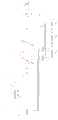
图1是多功能光中继器系统的示意图,由第一光纤(1)、双工模块(2)、光开关(3)、模式切换电路(4)、第一偏置电压电路(5)、接地接口(6)、第一开关单元(7)、第二偏置电压电路(8)、AGC放大均衡电路(9)、判决再生电路(10)、光源驱动(11)、第二开关单元(12)、第二光纤(13)、第三光纤(14)和第四光纤(15)组成。Figure 1 is a schematic diagram of a multifunctional optical repeater system, which consists of a first optical fiber (1), a duplex module (2), an optical switch (3), a mode switching circuit (4), and a first bias voltage circuit (5) , a grounding interface (6), a first switch unit (7), a second bias voltage circuit (8), an AGC amplification and equalization circuit (9), a judgment regeneration circuit (10), a light source driver (11), and a second switch unit (12), a second optical fiber (13), a third optical fiber (14) and a fourth optical fiber (15).
图2为双工模块的内部示意图,双工模块为一块集成光电子芯片,第一光纤(1)、第二光纤(3)与集成光电子芯片(2)进行耦合连接,双工模块中集成光电子芯片(2)可在不同的偏压下工作,上侧为整个模块的阴极(cathode),下侧为模块的阳极(anode);双工模块的工作原理为:双工模块是由有源区与无源区构成,有源区为增益区,当向双工模块中注入正向电流,并达到一定值时,其N区自由电子增多并不断进入量子阱中与空穴复合,以光子形式释放能量,该光子在输入光信号的感应下形成受激辐射,使释放出的光子和入射光子同频、同向、同相位、同偏振方向、同模式,并在光子不断前进中继续受感应而产生受激辐射,进而产生更多的新的光子,使输入光信号得到放大;对于宽带隙材料构成的量子阱结构,通过量子阱结构与掺杂的设计,在量子阱内形成特定的子能级,在波导层入射光的作用下,将量子阱结构双工模块中的电子从基态激发到激发态;通过外加反向偏置电压使激发态的电子形成电流,便可以得到光电流信号;进而整个双工模块在不同的偏置电压下可工作在光电转换和光信号放大两种工作模式下。Figure 2 is an internal schematic diagram of a duplex module. The duplex module is an integrated optoelectronic chip. The first optical fiber (1) and the second optical fiber (3) are coupled and connected to the integrated optoelectronic chip (2). The optoelectronic chip is integrated in the duplex module (2) It can work under different bias voltages, the upper side is the cathode (cathode) of the whole module, and the lower side is the anode (anode) of the module; the working principle of the duplex module is: the duplex module is composed of active area and The passive area is composed of the active area as the gain area. When the forward current is injected into the duplex module and reaches a certain value, the free electrons in the N area will increase and continuously enter the quantum well to recombine with holes and release them in the form of photons. The photon forms stimulated radiation under the induction of the input optical signal, so that the released photon and the incident photon have the same frequency, same direction, same phase, same polarization direction, and same mode, and continue to be induced as the photon continues to advance. Generate stimulated radiation, and then generate more new photons to amplify the input optical signal; for the quantum well structure composed of wide bandgap materials, through the design of the quantum well structure and doping, a specific sub-energy can be formed in the quantum well level, under the action of incident light in the waveguide layer, the electrons in the quantum well structure duplex module are excited from the ground state to the excited state; by applying a reverse bias voltage to make the electrons in the excited state form a current, the photocurrent signal can be obtained; Furthermore, the whole duplex module can work in two working modes of photoelectric conversion and optical signal amplification under different bias voltages.
图3是多功能光中继器系统的实施例示意图,单根输入光纤(1)、双工模块(2)、光开关(3)、模式切换电路(4)、第一偏置电压电路(5)、接地接口(6)、第一开关单元(7)、第二偏置电压电路(8)、AGC放大均衡电路(9)、判决再生电路(10)、光源驱动(11)、第二开关单元(12)、单根输出光纤(13)、第一光纤(14)和第二光纤(15)组成。双工模块(2)可在模式切换电路(4)的控制下工作在光电转换或光信号放大两种模式;当整个中继器系统工作在光-电-光模式下,模式切换电路(4)控制双工模块(2)上方的第二开关单元(12)连接第一偏置电压电路(5),控制双工模块(2)下方的第一开关单元(7)连接AGC放大均衡电路(9),对于双工模块(2)进行光电转换的光电流信号进行放大,并实现自动增益控制,使输入光信号在一定范围内变化时,输出电信号保持恒定输出;再将输出电信号输出到判决再生电路(10),判决再生电路(10)对于AGC放大均衡电路(9)输出的电信号进行识别判定并形成相应的数字信号;光源驱动(11)接收相应的数字信号并对光信号进行调制,并通过光开关(3)连接单根输出光纤(13)输出光信号,完成中继器的光信号接收和对信号进行整形再输出;当整个中继器系统工作在光信号放大模式,作为全光中继器功能工作时,模式切换电路(4)控制双工模块(2)上方的第二开关单元(12)连接接地接口(6),控制双工模块(2)下方的第一开关单元(7)连接第二偏置电压电路(8),为双工模块(2)中提供工作电压,对于输入的光信号进行放大,并通过光开关(3)连接单根输出光纤(13)将放大后的光信号进行输出,完成整个中继器进行光信号放大的功能。3 is a schematic diagram of an embodiment of a multifunctional optical repeater system, a single input optical fiber (1), a duplex module (2), an optical switch (3), a mode switching circuit (4), and a first bias voltage circuit ( 5), the ground interface (6), the first switch unit (7), the second bias voltage circuit (8), the AGC amplification and equalization circuit (9), the judgment regeneration circuit (10), the light source driver (11), the second It consists of a switch unit (12), a single output optical fiber (13), a first optical fiber (14) and a second optical fiber (15). The duplex module (2) can work in two modes of photoelectric conversion or optical signal amplification under the control of the mode switching circuit (4); when the entire repeater system works in the optical-electrical-optical mode, the mode switching circuit (4 ) controls the second switch unit (12) above the duplex module (2) to connect to the first bias voltage circuit (5), and controls the first switch unit (7) below the duplex module (2) to connect to the AGC amplification and equalization circuit ( 9), amplify the photocurrent signal of the duplex module (2) for photoelectric conversion, and realize automatic gain control, so that when the input optical signal changes within a certain range, the output electrical signal remains constant; and then the output electrical signal is output To the judgment regeneration circuit (10), the judgment regeneration circuit (10) recognizes and judges the electrical signal output by the AGC amplification and equalization circuit (9) and forms a corresponding digital signal; the light source driver (11) receives the corresponding digital signal and performs an optical signal Modulate, and connect a single output optical fiber (13) to output an optical signal through an optical switch (3), complete the optical signal reception of the repeater and reshape the signal before outputting; when the entire repeater system works in the optical signal amplification mode When working as an all-optical repeater, the mode switching circuit (4) controls the second switch unit (12) above the duplex module (2) to connect to the grounding interface (6), and controls the second switch unit (12) below the duplex module (2). A switch unit (7) is connected to the second bias voltage circuit (8), provides working voltage for the duplex module (2), amplifies the input optical signal, and connects a single output optical fiber ( 13) Outputting the amplified optical signal to complete the optical signal amplification function of the entire repeater.
具体实施方式Detailed ways
下面结合具体的实施例来进一步阐述本发明。The present invention will be further described below in conjunction with specific examples.
图3中给出多功能光中继器系统的实施例,它是由单根输入光纤(1)、双工模块(2)、光开关(3)、模式切换电路(4)、第一偏置电压电路(5)、接地接口(6)、第一开关单元(7)、第二偏置电压电路(8)、AGC放大均衡电路(9)、判决再生电路(10)、光源驱动(11)、第二开关单元(12)、单根输出光纤(13)、第一光纤(14)和第二光纤(15)组成。当在一些特殊地区环境使用时,通信接收端信号误码率较小,模式切换电路(4)通过控制第一开关单元(7)和第二开关单元(12)分别连接第二偏置电压电路(8)和接地接口(6),使双工模块(2)接正向偏置电压,工作在光信号放大模式下,同时控制光开关(3)与第一光纤(14)连接,将单根输出光纤(13)与双工模块(2)相连接,整个光中继器系统工作在光信号放大模式下,功耗较低;当遇到恶劣环境例如沙尘暴等环境、通信接收端信号误码率较大时;模式切换电路(4)控制双工模块(2)上方的第二开关单元(12)连接第一偏置电压电路(5),使双工模块(2)工作在反向偏置电压下,控制双工模块(2)下方的第一开关单元(7)连接AGC放大均衡电路(9),使双工模块(2)工作在反向偏置电压下,同时控制光开关(3)与第二光纤(15)连接,将单根输出光纤(13)连接至光源驱动(11);AGC放大均衡电路(9)对于双工模块(2)进行光电转换的光电流信号进行放大,并实现自动增益控制,使输入光信号在一定范围内变化时,输出电信号保持恒定输出;再将输出电信号输出到判决再生电路(10),判决再生电路(10)对于AGC放大均衡电路(9)输出的电信号进行识别判定并形成相应的数字信号;光源驱动(11)接收相应的数字信号对于光信号进行调制,并通过单根输出光纤(13)输出光信号,完成中继器的光信号接收和对信号进行整形再输出,通过整个中继器模式的切换,提升了信号的传输质量,使整个系统能够更加灵活的适用于各种环境。An embodiment of a multifunctional optical repeater system is provided in Fig. 3, which is composed of a single input optical fiber (1), a duplex module (2), an optical switch (3), a mode switching circuit (4), a first bias Setting voltage circuit (5), grounding interface (6), first switch unit (7), second bias voltage circuit (8), AGC amplification and equalization circuit (9), judgment regeneration circuit (10), light source driver (11 ), a second switch unit (12), a single output optical fiber (13), a first optical fiber (14) and a second optical fiber (15). When used in some special regional environments, the bit error rate of the signal at the communication receiving end is small, and the mode switching circuit (4) controls the first switch unit (7) and the second switch unit (12) to connect to the second bias voltage circuit respectively (8) and the grounding interface (6), so that the duplex module (2) is connected to the forward bias voltage, works in the optical signal amplification mode, and simultaneously controls the optical switch (3) to be connected to the first optical fiber (14), and the single The root output optical fiber (13) is connected to the duplex module (2), and the entire optical repeater system works in the optical signal amplification mode, and the power consumption is low; When the code rate is large; the mode switching circuit (4) controls the second switch unit (12) above the duplex module (2) to connect to the first bias voltage circuit (5), so that the duplex module (2) works in reverse Under the bias voltage, control the first switch unit (7) below the duplex module (2) to connect to the AGC amplification and equalization circuit (9), so that the duplex module (2) works under the reverse bias voltage and simultaneously controls the optical switch (3) be connected with the second optical fiber (15), the single output optical fiber (13) is connected to the light source driver (11); amplify and realize automatic gain control, so that when the input optical signal changes within a certain range, the output electrical signal remains constant; The electrical signal output by the circuit (9) is identified and judged to form a corresponding digital signal; the light source driver (11) receives the corresponding digital signal to modulate the optical signal, and outputs the optical signal through a single output optical fiber (13) to complete the relay The optical signal of the repeater is received and the signal is reshaped and then output. Through the switching of the entire repeater mode, the transmission quality of the signal is improved, so that the whole system can be more flexibly applied to various environments.
Claims (10)
Priority Applications (1)
| Application Number | Priority Date | Filing Date | Title |
|---|---|---|---|
| CN202110672401.1ACN113411132B (en) | 2021-06-17 | 2021-06-17 | Multifunctional optical repeater system |
Applications Claiming Priority (1)
| Application Number | Priority Date | Filing Date | Title |
|---|---|---|---|
| CN202110672401.1ACN113411132B (en) | 2021-06-17 | 2021-06-17 | Multifunctional optical repeater system |
Publications (2)
| Publication Number | Publication Date |
|---|---|
| CN113411132A CN113411132A (en) | 2021-09-17 |
| CN113411132Btrue CN113411132B (en) | 2023-03-31 |
Family
ID=77684746
Family Applications (1)
| Application Number | Title | Priority Date | Filing Date |
|---|---|---|---|
| CN202110672401.1AActiveCN113411132B (en) | 2021-06-17 | 2021-06-17 | Multifunctional optical repeater system |
Country Status (1)
| Country | Link |
|---|---|
| CN (1) | CN113411132B (en) |
Citations (1)
| Publication number | Priority date | Publication date | Assignee | Title |
|---|---|---|---|---|
| CN105378930A (en)* | 2013-06-19 | 2016-03-02 | 欧培拉太阳能公司 | Optoelectronic integrated circuit |
Family Cites Families (5)
| Publication number | Priority date | Publication date | Assignee | Title |
|---|---|---|---|---|
| US7723139B2 (en)* | 2007-10-01 | 2010-05-25 | Corning Incorporated | Quantum well intermixing |
| CN101877455B (en)* | 2009-04-28 | 2013-02-06 | 高质激光有限公司 | Laser amplifier system and laser amplifier method |
| JP6172789B2 (en)* | 2013-03-08 | 2017-08-02 | 国立大学法人京都大学 | Laser equipment |
| CN109100018B (en)* | 2018-07-26 | 2021-08-03 | 传周半导体科技(上海)有限公司 | Large-dynamic-range weak light detection system based on avalanche photodiode array chip |
| CN112566312B (en)* | 2020-12-09 | 2023-04-07 | 苏州亮芯光电科技有限公司 | Multifunctional device based on quantum well diode array chip and control method thereof |
- 2021
- 2021-06-17CNCN202110672401.1Apatent/CN113411132B/enactiveActive
Patent Citations (1)
| Publication number | Priority date | Publication date | Assignee | Title |
|---|---|---|---|---|
| CN105378930A (en)* | 2013-06-19 | 2016-03-02 | 欧培拉太阳能公司 | Optoelectronic integrated circuit |
Also Published As
| Publication number | Publication date |
|---|---|
| CN113411132A (en) | 2021-09-17 |
Similar Documents
| Publication | Publication Date | Title |
|---|---|---|
| Matsuura et al. | Over 40-W electric power and optical data transmission using an optical fiber | |
| CN201821352U (en) | Free space photo-communication device based on passive optical network | |
| CN101656575A (en) | Free space optical communication device based on passive optical network (PON) | |
| CN104348553A (en) | Cfp optical transceiver module | |
| WO2013189422A2 (en) | Light receiving device and method, and light transceiving integrated module | |
| Chen et al. | Visible light communication based on computational temporal ghost imaging and micro-LED-based detector | |
| Umezawa et al. | Multi-core based 94-GHz radio and power over fiber transmission using 100-GHz analog photoreceiver | |
| Abbasi et al. | 100-Gb/s electro-absorptive duobinary modulation of an InP-on-Si DFB laser | |
| CN109743113B (en) | Optical module and optical line terminal | |
| CN111585654A (en) | Low-power consumption far-end antenna unit implementation method and far-end antenna device | |
| CN103929252A (en) | A Coherent Receiver Based on Avalanche Photodiode APD | |
| Pinto et al. | Power-over-fiber-based optical wireless communication systems towards 6G | |
| CN107658927A (en) | Adaptive mobile optics charging system based on feedback signaling | |
| CN113036949A (en) | Laser energy supply device based on photocell | |
| Krishnamoorthy et al. | Optical wireless communications: enabling the next generation network of networks | |
| CN203563070U (en) | Cfp optical transceiver module | |
| CN113411132B (en) | Multifunctional optical repeater system | |
| CN102202245B (en) | Method, device and system for processing signals | |
| Hasebe et al. | 28-Gbit/s 80-km transmission using SOA-assisted extended-reach EADFB laser (AXEL) | |
| CN113783317A (en) | System and method for co-transmission of energy and information based on few-mode fiber | |
| Kwon et al. | Fabrication of 40 Gb/s Front‐End Optical Receivers Using Spot‐Size Converter Integrated Waveguide Photodiodes | |
| Manzoor et al. | Leveraging InGaN solar cells for visible light communication reception | |
| CN106788776A (en) | A kind of photodetector and opto-electronic conversion method | |
| Buchali et al. | Amplifier less 400 Gb/s coherent transmission at short reach | |
| CN106899352B (en) | Photoelectric conversion device based on QSFP28 optical module |
Legal Events
| Date | Code | Title | Description |
|---|---|---|---|
| PB01 | Publication | ||
| PB01 | Publication | ||
| SE01 | Entry into force of request for substantive examination | ||
| SE01 | Entry into force of request for substantive examination | ||
| GR01 | Patent grant | ||
| GR01 | Patent grant |