CN113410375B - An LED light source module and LED hair removal device for hair removal - Google Patents
An LED light source module and LED hair removal device for hair removalDownload PDFInfo
- Publication number
- CN113410375B CN113410375BCN202110744103.9ACN202110744103ACN113410375BCN 113410375 BCN113410375 BCN 113410375BCN 202110744103 ACN202110744103 ACN 202110744103ACN 113410375 BCN113410375 BCN 113410375B
- Authority
- CN
- China
- Prior art keywords
- area
- hair removal
- led
- light source
- conductive patch
- Prior art date
- Legal status (The legal status is an assumption and is not a legal conclusion. Google has not performed a legal analysis and makes no representation as to the accuracy of the status listed.)
- Active
Links
Images


Classifications
- H—ELECTRICITY
- H10—SEMICONDUCTOR DEVICES; ELECTRIC SOLID-STATE DEVICES NOT OTHERWISE PROVIDED FOR
- H10H—INORGANIC LIGHT-EMITTING SEMICONDUCTOR DEVICES HAVING POTENTIAL BARRIERS
- H10H20/00—Individual inorganic light-emitting semiconductor devices having potential barriers, e.g. light-emitting diodes [LED]
- H10H20/80—Constructional details
- H10H20/85—Packages
- H10H20/858—Means for heat extraction or cooling
- H10H20/8581—Means for heat extraction or cooling characterised by their material
- A—HUMAN NECESSITIES
- A61—MEDICAL OR VETERINARY SCIENCE; HYGIENE
- A61B—DIAGNOSIS; SURGERY; IDENTIFICATION
- A61B18/00—Surgical instruments, devices or methods for transferring non-mechanical forms of energy to or from the body
- A61B18/18—Surgical instruments, devices or methods for transferring non-mechanical forms of energy to or from the body by applying electromagnetic radiation, e.g. microwaves
- A61B18/20—Surgical instruments, devices or methods for transferring non-mechanical forms of energy to or from the body by applying electromagnetic radiation, e.g. microwaves using laser
- H—ELECTRICITY
- H01—ELECTRIC ELEMENTS
- H01L—SEMICONDUCTOR DEVICES NOT COVERED BY CLASS H10
- H01L25/00—Assemblies consisting of a plurality of semiconductor or other solid state devices
- H01L25/03—Assemblies consisting of a plurality of semiconductor or other solid state devices all the devices being of a type provided for in a single subclass of subclasses H10B, H10D, H10F, H10H, H10K or H10N, e.g. assemblies of rectifier diodes
- H01L25/04—Assemblies consisting of a plurality of semiconductor or other solid state devices all the devices being of a type provided for in a single subclass of subclasses H10B, H10D, H10F, H10H, H10K or H10N, e.g. assemblies of rectifier diodes the devices not having separate containers
- H01L25/075—Assemblies consisting of a plurality of semiconductor or other solid state devices all the devices being of a type provided for in a single subclass of subclasses H10B, H10D, H10F, H10H, H10K or H10N, e.g. assemblies of rectifier diodes the devices not having separate containers the devices being of a type provided for in group H10H20/00
- H01L25/0753—Assemblies consisting of a plurality of semiconductor or other solid state devices all the devices being of a type provided for in a single subclass of subclasses H10B, H10D, H10F, H10H, H10K or H10N, e.g. assemblies of rectifier diodes the devices not having separate containers the devices being of a type provided for in group H10H20/00 the devices being arranged next to each other
- H—ELECTRICITY
- H10—SEMICONDUCTOR DEVICES; ELECTRIC SOLID-STATE DEVICES NOT OTHERWISE PROVIDED FOR
- H10H—INORGANIC LIGHT-EMITTING SEMICONDUCTOR DEVICES HAVING POTENTIAL BARRIERS
- H10H20/00—Individual inorganic light-emitting semiconductor devices having potential barriers, e.g. light-emitting diodes [LED]
- H10H20/80—Constructional details
- H10H20/85—Packages
- H10H20/8506—Containers
- H—ELECTRICITY
- H10—SEMICONDUCTOR DEVICES; ELECTRIC SOLID-STATE DEVICES NOT OTHERWISE PROVIDED FOR
- H10H—INORGANIC LIGHT-EMITTING SEMICONDUCTOR DEVICES HAVING POTENTIAL BARRIERS
- H10H20/00—Individual inorganic light-emitting semiconductor devices having potential barriers, e.g. light-emitting diodes [LED]
- H10H20/80—Constructional details
- H10H20/85—Packages
- H10H20/857—Interconnections, e.g. lead-frames, bond wires or solder balls
- H—ELECTRICITY
- H10—SEMICONDUCTOR DEVICES; ELECTRIC SOLID-STATE DEVICES NOT OTHERWISE PROVIDED FOR
- H10H—INORGANIC LIGHT-EMITTING SEMICONDUCTOR DEVICES HAVING POTENTIAL BARRIERS
- H10H20/00—Individual inorganic light-emitting semiconductor devices having potential barriers, e.g. light-emitting diodes [LED]
- H10H20/80—Constructional details
- H10H20/85—Packages
- H10H20/858—Means for heat extraction or cooling
- H10H20/8585—Means for heat extraction or cooling being an interconnection
- A—HUMAN NECESSITIES
- A61—MEDICAL OR VETERINARY SCIENCE; HYGIENE
- A61B—DIAGNOSIS; SURGERY; IDENTIFICATION
- A61B18/00—Surgical instruments, devices or methods for transferring non-mechanical forms of energy to or from the body
- A61B2018/00005—Cooling or heating of the probe or tissue immediately surrounding the probe
- A—HUMAN NECESSITIES
- A61—MEDICAL OR VETERINARY SCIENCE; HYGIENE
- A61B—DIAGNOSIS; SURGERY; IDENTIFICATION
- A61B18/00—Surgical instruments, devices or methods for transferring non-mechanical forms of energy to or from the body
- A61B2018/00315—Surgical instruments, devices or methods for transferring non-mechanical forms of energy to or from the body for treatment of particular body parts
- A61B2018/00452—Skin
- A61B2018/00476—Hair follicles
- A—HUMAN NECESSITIES
- A61—MEDICAL OR VETERINARY SCIENCE; HYGIENE
- A61B—DIAGNOSIS; SURGERY; IDENTIFICATION
- A61B18/00—Surgical instruments, devices or methods for transferring non-mechanical forms of energy to or from the body
- A61B18/18—Surgical instruments, devices or methods for transferring non-mechanical forms of energy to or from the body by applying electromagnetic radiation, e.g. microwaves
- A61B2018/1807—Surgical instruments, devices or methods for transferring non-mechanical forms of energy to or from the body by applying electromagnetic radiation, e.g. microwaves using light other than laser radiation
Landscapes
- Health & Medical Sciences (AREA)
- Engineering & Computer Science (AREA)
- Surgery (AREA)
- Physics & Mathematics (AREA)
- Life Sciences & Earth Sciences (AREA)
- Medical Informatics (AREA)
- Public Health (AREA)
- Nuclear Medicine, Radiotherapy & Molecular Imaging (AREA)
- Biomedical Technology (AREA)
- Heart & Thoracic Surgery (AREA)
- Electromagnetism (AREA)
- Molecular Biology (AREA)
- Animal Behavior & Ethology (AREA)
- General Health & Medical Sciences (AREA)
- Otolaryngology (AREA)
- Veterinary Medicine (AREA)
- Microelectronics & Electronic Packaging (AREA)
- Power Engineering (AREA)
- Condensed Matter Physics & Semiconductors (AREA)
- General Physics & Mathematics (AREA)
- Optics & Photonics (AREA)
- Computer Hardware Design (AREA)
- Led Device Packages (AREA)
Abstract
Description
Translated fromChinese技术领域technical field
本发明属于光学脱毛技术领域,尤其涉及一种用于脱毛的LED光源模组与LED脱毛仪。The invention belongs to the technical field of optical hair removal, and in particular relates to an LED light source module for hair removal and an LED hair removal instrument.
背景技术Background technique
现有的家用脱毛仪大多采用激光或IPL(Intense pulsed light,强脉冲光)作为光源来进行脱毛,由于皮肤毛囊中黑色素的含量较高,而黑色素对光有较强的吸收作用,因此当激光或IPL在穿过表层皮肤到达毛囊层后,毛囊可将光能转化为热能,若是黑色素在短时间内吸收激光或IPL所携带的光能并将之转化为热能后,可破坏甚至是进一步的杀死毛囊,使得毛囊内的毛发短时间或长时间不再生,以达到脱毛的目的。Most of the existing household hair removal devices use laser or IPL (Intense pulsed light, intense pulsed light) as the light source for hair removal. Due to the high content of melanin in the skin hair follicles, melanin has a strong absorption effect on light, so when the laser is used Or after IPL passes through the superficial skin and reaches the hair follicle layer, the hair follicle can convert light energy into heat energy. If melanin absorbs the light energy carried by the laser or IPL in a short time and converts it into heat energy, it can destroy or even further. Killing the hair follicle, so that the hair in the follicle does not regenerate for a short time or a long time, so as to achieve the purpose of hair removal.
基于激光光源的脱毛仪中,由于激光器光谱单一,并且出光口较小,即激光照射到皮肤上的光斑面积较小、较为集中,在对大面积的皮肤进行脱毛时,需要用户多次主动地操控脱毛仪移动脱毛,操作较为频繁,脱毛效率较为低下,用户体验不佳。并且,由于光斑面积的限制,还容易因频繁密集的操作增加对同一脱毛区域重复脱毛的几率,提高了因光斑重叠而带来的皮肤风险。由于激光的能量较大,也可能因不慎操作而对人体造成伤害。In the hair removal device based on the laser light source, due to the single laser spectrum and the small light outlet, that is, the laser spot area on the skin is small and concentrated, when removing hair on a large area of the skin, the user needs to actively take the initiative to many times. Controlling the hair removal device to move hair removal is more frequent, the hair removal efficiency is relatively low, and the user experience is not good. Moreover, due to the limitation of the spot area, it is easy to increase the probability of repeated depilation of the same depilation area due to frequent and intensive operations, which increases the risk of skin caused by overlapping spots. Due to the high energy of the laser, it may also cause harm to the human body due to careless operation.
基于IPL光源的脱毛仪中,由于IPL光源为自发辐射光源,其所发出光的波长范围过大,大概为300-1200nm,其中包含了短波长范围(300-470nm)的光。而短波长范围的光容易对人体造成伤害,例如紫外光(300-370nm)不但容易被人体吸收而导致皮肤的黑色素沉积,导致肤色变深甚至变黑,若是不慎照射到人眼,还可能对人眼造成伤害。In the hair removal device based on the IPL light source, since the IPL light source is a spontaneous radiation light source, the wavelength range of the light emitted is too large, about 300-1200nm, which includes light in the short wavelength range (300-470nm). Light in the short wavelength range is easy to cause harm to the human body. For example, ultraviolet light (300-370 nm) is not only easily absorbed by the human body, which leads to the deposition of melanin on the skin, resulting in darkening or even darkening of the skin. If it is accidentally irradiated to the human eye, it may also Causes damage to human eyes.
并且,IPL光源发出的所有光中,只有一部分波长范围(大概在600-1200nm)的光能用于脱毛,300-600nm波长范围的光并不具备脱毛效果。因此,对于IPL光源的脱毛仪来说,在实际的使用过程中,必须通过滤光片过滤短波长的有害光,得到所需波长范围的光进行使用,对总发光能量的利用率较低。Moreover, of all the light emitted by the IPL light source, only a part of the wavelength range (about 600-1200nm) can be used for hair removal, and the light in the 300-600nm wavelength range has no hair removal effect. Therefore, for the hair removal device of the IPL light source, in the actual use process, the harmful light of short wavelength must be filtered through the filter to obtain the light of the required wavelength range for use, and the utilization rate of the total luminous energy is low.
鉴于激光光源与IPL光源的上述缺陷,现有技术中已有采用LED光源替代激光光源与IPL光源应用于脱毛仪中的尝试,但在将LED光源应用于脱毛仪中时,不但要考虑到LED光源输出的能量能否有效脱毛,还要考虑到LED光源的散热与功耗问题。In view of the above-mentioned defects of the laser light source and the IPL light source, there have been attempts in the prior art to use the LED light source to replace the laser light source and the IPL light source in the hair removal device. Whether the energy output by the light source can effectively remove hair, the heat dissipation and power consumption of the LED light source must also be considered.
LED光源的有效发光面积为其内的LED芯片的发光面积,而并不包括LED光源中本身不发光的区域的面积,可以理解的是,LED光源的有效发光面积越大,则发热量与功耗也越大,而若是减小有效发光面积,虽然能降低LED光源的发热量与功耗,但对大面积皮肤脱毛时,需要用户频繁操作脱毛仪脱毛,脱毛效率较低,并且LED光源的结构也会相对不够紧凑与小型化。因此,如何合理地设计LED光源的结构参数与电气参数,以平衡LED光源的有效发光面积、散热、功耗与小型化结构要求等重要因素之间的关系,是将LED光源应用于脱毛仪时需要重点解决的问题。The effective light-emitting area of the LED light source is the light-emitting area of the LED chip inside it, and does not include the area of the area in the LED light source that does not emit light. The power consumption is also greater, and if the effective light-emitting area is reduced, although the heat generation and power consumption of the LED light source can be reduced, when removing hair on a large area of skin, the user needs to operate the epilator frequently to remove hair, and the hair removal efficiency is low. The structure will also be relatively less compact and miniaturized. Therefore, how to reasonably design the structural parameters and electrical parameters of the LED light source to balance the relationship between the effective luminous area, heat dissipation, power consumption and miniaturized structure requirements of the LED light source is the most important factor when applying the LED light source to the hair removal device. issues that need to be addressed.
并且,由于LED光源一般作为照明光源来使用,现有技术中一般直接将LED芯片设置于PCB板上,再将多个LED芯片直接串联或并联在一起,但是多个LED芯片的位置关系以及走线布线等电气设计,会影响LED光源中本身不发光的区域的面积,而与LED光源的有效发光面积直接相关。In addition, since LED light sources are generally used as illumination light sources, in the prior art, LED chips are generally directly arranged on the PCB board, and then multiple LED chips are directly connected in series or parallel. Electrical design such as wire wiring will affect the area of the LED light source that does not emit light itself, which is directly related to the effective light emitting area of the LED light source.
因此,若仅是简单的从照明角度上设计多个LED芯片的位置关系,而不考虑到LED芯片的结构设计与电气设计对有效发光面积、散热、功耗与小型化结构要求等重要因素的影响,现有的LED光源将会难以适用于脱毛仪中。Therefore, if the positional relationship of multiple LED chips is simply designed from the perspective of lighting, the structural design and electrical design of the LED chips are not considered to be important factors such as effective light-emitting area, heat dissipation, power consumption and miniaturized structure requirements. Influence, the existing LED light source will be difficult to apply to the hair removal device.
发明内容SUMMARY OF THE INVENTION
本发明实施例提供一种用于脱毛的LED光源模组,旨在解决现有的LED光源的结构设计与电气设计难以满足应用于脱毛仪时对有效发光面积、散热、功耗以及小型化结构等要求的技术问题。Embodiments of the present invention provide an LED light source module for hair removal, which aims to solve the problem that the structural design and electrical design of the existing LED light source are difficult to meet the requirements for effective light emitting area, heat dissipation, power consumption and miniaturized structure when applied to a hair removal device. and other required technical issues.
本发明实施例是这样实现的,一种用于脱毛的LED光源模组,包括金属基板与焊接于所述金属基板上的陶瓷板,所述用于脱毛的LED光源模组还包括:The embodiments of the present invention are implemented in this way. An LED light source module for hair removal includes a metal substrate and a ceramic plate welded on the metal substrate. The LED light source module for hair removal further includes:
设置于所述陶瓷板上的2个或2个以上相互独立的导电贴片区;two or more mutually independent conductive patch areas arranged on the ceramic board;
每个所述导电贴片区上设置有多个互相连接的LED芯片,以及一个供临近的所述导电贴片区中的多个所述LED芯片连接的共线区域;Each of the conductive patch areas is provided with a plurality of LED chips connected to each other, and a collinear area for connecting a plurality of the LED chips in the adjacent conductive patch areas;
所述导电贴片区的面积为k*nS,所述共线区域的面积为t*S,其中,S为单个所述LED芯片的面积,n为所述导电贴片区中的所述LED芯片的数量,k为贴片容余系数,t为连线裕度系数;The area of the conductive patch area is k*nS, and the area of the collinear area is t*S, where S is the area of a single LED chip, and n is the LED in the conductive patch area The number of chips, k is the chip allowance coefficient, t is the connection allowance coefficient;
所述贴片容余系数k满足1.3<k≤3.9,所述连线裕度系数t满足0.1<t≤3.3。The patch margin coefficient k satisfies 1.3<k≦3.9, and the connection margin coefficient t satisfies 0.1<t≦3.3.
更进一步地,每个所述导电贴片区中的多个所述LED芯片之间并联连接。Further, a plurality of the LED chips in each of the conductive patch regions are connected in parallel.
更进一步地,任意两个所述导电贴片区之间串联连接。Further, any two of the conductive patch regions are connected in series.
更进一步地,每个所述导电贴片区中设置有3个并联连接的所述LED芯片。Furthermore, each of the conductive patch regions is provided with three LED chips connected in parallel.
更进一步地,所述导电贴片区的每个所述LED芯片的顶部电极连接至另一所述导电贴片区的所述共线区域。Further, the top electrode of each of the LED chips of the conductive patch area is connected to the collinear area of the other conductive patch area.
更进一步地,多个所述导电贴片区连接后配置为至少2个独立或者组合发光的发光区。Furthermore, the plurality of conductive patch regions are connected and configured to form at least two light-emitting regions that emit light independently or in combination.
更进一步地,所述发光区配置为2-25个。Further, there are 2-25 light-emitting regions.
更进一步地,所述贴片容余系数k满足:1.3<k≤2.1。Further, the patch allowance coefficient k satisfies: 1.3<k≤2.1.
更进一步地,所述连线裕度系数t满足0.45<t≤1.9。Further, the connection margin coefficient t satisfies 0.45<t≤1.9.
本发明实施例还提供了一种LED脱毛仪,其包括:The embodiment of the present invention also provides an LED hair removal device, which includes:
控制器、驱动电源与散热结构;以及a controller, a drive power supply, and a heat dissipation structure; and
如上述任一项所述的用于脱毛的LED光源模组;The LED light source module for hair removal according to any one of the above;
所述控制器与所述驱动电源、所述散热结构以及所述用于脱毛的LED光源模组分别连接,所述驱动电源还与所述散热结构以及所述用于脱毛的LED光源模组分别连接。The controller is respectively connected with the driving power source, the heat dissipation structure and the LED light source module for hair removal, and the driving power source is also connected with the heat dissipation structure and the LED light source module for hair removal respectively. connect.
本发明所达到的有益效果是,基于LED芯片的有效发光面积nS来设计导电贴片区的面积k*nS,基于单个LED芯片的面积S来设计共线区域的面积t*S,为整个导电贴片区留下适合用于走线、布线等电气设计的空间,避免现有技术中LED光源简单的走线、布线等电气设计无法与脱毛仪的小型化结构、有效发光面积、功率密度以及散热等需求相适应。The beneficial effect achieved by the present invention is that the area k*nS of the conductive patch area is designed based on the effective light-emitting area nS of the LED chip, and the area t*S of the collinear area is designed based on the area S of a single LED chip, which is the overall conductive area The patch area leaves space suitable for electrical design such as wiring and wiring, avoiding that the simple wiring, wiring and other electrical designs of the LED light source in the prior art cannot be compared with the miniaturized structure, effective light-emitting area, power density and meet the needs of heat dissipation.
结合用于脱毛的LED光源模组具体应用时不同的结构、有效发光面积、脱毛能量以及散热等需求,来预先设计得到贴片容余系数k以及连线裕度系数t,结合LED芯片的有效发光面积,以确定导电贴片区以及共线区域的面积,在确定导电贴片区面积、共线区域面积以及有效发光面积后,即可结合实际需求和现阶段生产工艺合理地设计LED芯片的排布位置与间隙等结构参数以及走线布线等电气参数,可在保证有效散热的基础上将用于脱毛的LED光源模组设计成紧凑、小型化的结构,以进一步地满足将用于脱毛的LED光源模组应用于脱毛仪时的对脱毛能量、小型化与散热等需求,实现用于脱毛的LED光源模组在脱毛仪中的有效应用。Combined with the specific application of the LED light source module for hair removal, the different structures, effective light-emitting area, hair removal energy and heat dissipation requirements are pre-designed to obtain the patch allowance coefficient k and the connection allowance coefficient t. Combined with the effectiveness of the LED chip The light-emitting area is to determine the area of the conductive patch area and the collinear area. After determining the area of the conductive patch area, the area of the collinear area and the effective light-emitting area, you can reasonably design the LED chip according to the actual needs and the current production process. Structural parameters such as arrangement position and clearance, as well as electrical parameters such as wiring, can design the LED light source module for hair removal into a compact and miniaturized structure on the basis of ensuring effective heat dissipation, so as to further meet the requirements for hair removal. The LED light source module used for hair removal requires energy, miniaturization and heat dissipation for hair removal, so as to realize the effective application of the LED light source module for hair removal in the hair removal device.
附图说明Description of drawings
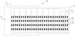
图1是本发明实施例提供的用于脱毛的LED光源模组的平面示意图;1 is a schematic plan view of an LED light source module for hair removal provided by an embodiment of the present invention;
图2是图1的用于脱毛的LED光源模组在A1-A1向的截面示意图;2 is a schematic cross-sectional view of the LED light source module for hair removal of FIG. 1 in the direction A1-A1;
图3是本发明实施例提供的LED芯片组的控制电路示意图;3 is a schematic diagram of a control circuit of an LED chip set provided by an embodiment of the present invention;
图4是本发明实施例提供的发光区的平面示意图;4 is a schematic plan view of a light-emitting region provided by an embodiment of the present invention;
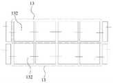
图5是本发明实施例提供的导电贴片区的平面示意图;5 is a schematic plan view of a conductive patch area provided by an embodiment of the present invention;
图6是本发明一个实施例提供的导电贴片区的平面示意图;6 is a schematic plan view of a conductive patch area provided by an embodiment of the present invention;
图7是本发明一个实施例提供的导电贴片区无共线区域时的平面示意图;7 is a schematic plan view of the conductive patch area provided by an embodiment of the present invention when there is no collinear area;
图8是本发明另一个实施例提供的导电贴片区的平面示意图;8 is a schematic plan view of a conductive patch area provided by another embodiment of the present invention;
图9是本发明另一个实施例提供的导电贴片区无共线区域时的平面示意图;9 is a schematic plan view of the conductive patch area provided by another embodiment of the present invention when there is no collinear area;
图10是本发明又一个实施例提供的导电贴片区的平面示意图;10 is a schematic plan view of a conductive patch area provided by another embodiment of the present invention;
图11是本发明又一个实施例提供的导电贴片区无共线区域时的平面示意图;11 is a schematic plan view of a conductive patch area provided by another embodiment of the present invention when there is no collinear area;
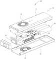
图12是本发明实施例提供的LED脱毛仪的立体分解示意图;Fig. 12 is a perspective exploded schematic diagram of an LED hair removal device provided by an embodiment of the present invention;
图13是本发明实施例提供的LED脱毛仪的立体示意图;13 is a schematic perspective view of an LED hair removal device provided by an embodiment of the present invention;
图14是本发明实施例提供的LED脱毛仪的另一立体示意图。FIG. 14 is another perspective schematic diagram of the LED hair removal device provided by the embodiment of the present invention.
具体实施方式Detailed ways
为了使本发明的目的、技术方案及优点更加清楚明白,以下结合附图及实施例,对本发明进行进一步详细说明。应当理解,此处所描述的具体实施例仅仅用以解释本发明,并不用于限定本发明。In order to make the objectives, technical solutions and advantages of the present invention clearer, the present invention will be further described in detail below with reference to the accompanying drawings and embodiments. It should be understood that the specific embodiments described herein are only used to explain the present invention, but not to limit the present invention.
现有技术中已有将LED光源应用于脱毛仪的尝试,一般选用多个LED芯片组成LED光源并尽可能地缩短多个LED芯片之间的间隙,提升LED光源在单位面积上所输出的能量,满足脱毛需求。但是,尽可能地缩短多个LED芯片之间的间隙存在一定的技术难度,多个LED芯片紧密排布时,同样会存在较大的散热问题,并且LED芯片对温度较为敏感,当自身的温度接近或超过结温时,会导致自身的光衰减,温度升高的同时还会影响自身的光电转换效率,而影响整体LED光源的能量输出。In the prior art, there have been attempts to apply LED light sources to hair removal devices. Generally, multiple LED chips are used to form an LED light source and the gap between the multiple LED chips is shortened as much as possible to increase the output energy of the LED light source per unit area. , to meet the needs of hair removal. However, it is technically difficult to shorten the gap between multiple LED chips as much as possible. When multiple LED chips are closely arranged, there will also be a large heat dissipation problem, and the LED chips are more sensitive to temperature. When it approaches or exceeds the junction temperature, it will cause its own light attenuation. When the temperature rises, it will also affect its own photoelectric conversion efficiency, which will affect the energy output of the overall LED light source.
LED光源为光热元件,驱动LED光源工作的电功率一部分被LED光源由电能转化为光能,另一部分由电能转化为热能。当LED光源的光电转化效率提升时,发热量相对降低,当LED光源的光电转化效率降低时,发热量则相对提高。现有的LED光源的光电转化率一般在30-40%之间,即LED光源发光时大部分的功率都转化为热量,因此对LED光源进行有效散热尤为重要。The LED light source is a photothermal element, and part of the electric power driving the LED light source is converted from electrical energy into light energy by the LED light source, and the other part is converted from electrical energy into thermal energy. When the photoelectric conversion efficiency of the LED light source is increased, the calorific value is relatively reduced, and when the photoelectric conversion efficiency of the LED light source is decreased, the calorific value is relatively increased. The photoelectric conversion rate of the existing LED light source is generally between 30-40%, that is, most of the power of the LED light source is converted into heat when it emits light, so it is particularly important to effectively dissipate the LED light source.
更多地,在考虑到LED光源的散热的同时,还要考虑到LED光源的结构参数设置与电气参数设置,由于现有的LED光源一般仅是作为照明光源使用,结构相对简单,LED芯片之间为简单的串并联关系,对自身的结构并无体积要求与限制,因此大功率的LED光源的体积为满足散热需求一般设计的较大,现有技术中一般难以在满足大功率要求的同时实现LED光源的小型化。More, while considering the heat dissipation of the LED light source, the structural parameter setting and electrical parameter setting of the LED light source should also be considered. Since the existing LED light source is generally only used as a lighting light source, the structure is relatively simple, and the LED chip is relatively simple. There is a simple series-parallel relationship, and there are no volume requirements and restrictions on its own structure. Therefore, the volume of high-power LED light sources is generally designed to meet the heat dissipation requirements. Realize the miniaturization of LED light source.
并且,若只是为了实现照明,LED光源中的LED芯片一般是直接设置于PCB板上,LED芯片的走线、布线等电气参数设计满足正常的开关控制即可,走线、布线等电气设计相对简单、要求较低。Moreover, if it is only for lighting, the LED chip in the LED light source is generally directly arranged on the PCB board, and the electrical parameters such as the wiring and wiring of the LED chip can be designed to meet the normal switch control. The electrical design of wiring and wiring is relatively Simple and less demanding.
而LED光源用于脱毛时,为在单位面积内输出尽量大的光能量,则需要在单位面积内设置尽可能多的LED芯片,因此,在合适的范围内,LED芯片的尺寸、体积越小越好,此时采用的用于脱毛的LED芯片的尺寸相对用作光源的LED芯片来说体积明显缩小,由厘米级直接降到毫米级甚至是纳米级,对用于脱毛的LED芯片的走线、布线等电气设计要求也越来越高。When the LED light source is used for hair removal, in order to output as much light energy as possible per unit area, it is necessary to set as many LED chips as possible in the unit area. Therefore, within a suitable range, the smaller the size and volume of the LED chip The better, the size of the LED chip used for hair removal at this time is significantly smaller than that of the LED chip used as a light source, from the centimeter level directly to the millimeter level or even the nanometer level. Electrical design requirements such as wires and wiring are also getting higher and higher.
但是,当LED芯片之间的距离过小时,可能导致LED芯片之间接触、无法相互绝缘而导电,影响LED芯片的正常工作,因此要合理的设计LED芯片之间的距离。同时,还要考虑到LED芯片的有效发光面积、散热、功耗以及结构小型化等要求,以得到一个性能与结构综合最佳的方案。若以现有LED光源的照明标准来设计用于脱毛的LED光源,在高功率、小型化、散热快、能量输出高等实际脱毛应用的要求下,明显无法达成。However, when the distance between the LED chips is too small, it may lead to contact between the LED chips, which cannot be insulated from each other and conduct electricity, which affects the normal operation of the LED chips. Therefore, the distance between the LED chips should be reasonably designed. At the same time, the requirements of the effective light-emitting area, heat dissipation, power consumption and structure miniaturization of the LED chip should be considered to obtain a solution with the best combination of performance and structure. If the LED light source for hair removal is designed according to the lighting standards of the existing LED light source, it is obviously impossible to achieve the actual hair removal application requirements of high power, miniaturization, fast heat dissipation, and high energy output.
实施例一Example 1
请参阅图1至图3,本发明实施例的用于脱毛的LED光源模组10,包括金属基板11与焊接于金属基板11上的陶瓷板12。陶瓷板12上设置有2个或2个以上相互独立的导电贴片区13。每个导电贴片区13上设置有多个互相连接的LED芯片132,以及一个供临近的导电贴片区13中的多个LED芯片132连接的共线区域131。导电贴片区13的面积为k*nS,共线区域131的面积为t*S,其中,S为单个LED芯片132的面积,n为导电贴片区13中的LED芯片132的数量,k为贴片容余系数,t为连线裕度系数,贴片容余系数k满足1.3<k≤3.9,连线裕度系数t满足0.1<t≤3.3。Referring to FIGS. 1 to 3 , the LED
本发明实施例的用于脱毛的LED光源模组10中,用于脱毛的LED光源模组10由上至下为LED芯片132、陶瓷板12以及金属基板11的结构分布,以金属基板11作为用于脱毛的LED光源模组10的底层承载以及散热的结构,金属基板11具有较高的导热系数、较低的热阻和较高的强度,可有效地将其上的陶瓷板12以及LED芯片132产生的热量导出用于脱毛的LED光源模组10,保证用于脱毛的LED光源模组10的散热效果和正常工作,提升使用寿命。In the LED
陶瓷板12上刻蚀有驱动电路,以实现对2个或2个以上相互独立的导电贴片区13的控制,进一步地实现对多个互相连接的LED芯片132精准、有效地控制。并且,陶瓷板12也具备较佳的电绝缘性能,因而2个或2个以上的导电贴片区13之间相互绝缘、独立,工作时相互之间不会发生干扰,进一步实现对导电贴片区13的独立控制。A driving circuit is etched on the
同时,陶瓷板12也具备较高的导热系数与较低的热阻,可在LED芯片132发热时,有效地将其产生的热量传导至金属基板11进行散热,进一步地提升对LED芯片132的散热效果,保证用于脱毛的LED光源模组10的正常工作。At the same time, the
在本发明实施例中,用于脱毛的LED光源模组10的散热需求一部分由陶瓷板12与金属基板11满足,另一部分散热需求由对用于脱毛的LED光源模组10的发光控制来满足,对脱毛能量、小型化要求则由对于导电贴片区13的具体设置来实现。In the embodiment of the present invention, part of the heat dissipation requirement of the LED
通过将导电贴片区13的面积设计为k*nS,将共线区域131的面积设计为t*S,其中S为单个LED芯片132的面积,n为导电贴片区13中的LED芯片132的数量,而k为贴片容余系数,t为连线裕度系数,即基于多个LED芯片132的总有效发光面积nS来设计导电贴片区13的面积k*nS,基于单个LED芯片132的有效发光面积S来设计共线区域131的面积t*S,为整个导电贴片区13留下适合用于走线、布线的空间,避免现有技术中LED光源简单的走线、布线等电气设计无法与对脱毛仪的小型化结构、有效发光面积、脱毛能量以及散热等需求相适应。By designing the area of the
结合用于脱毛的LED光源模组10在具体应用时不同的结构、有效发光面积、脱毛能量以及散热等需求,来预先设计得到贴片容余系数k以及连线裕度系数t,结合LED芯片132的有效发光面积,以确定导电贴片区13以及共线区域131的面积,在确定导电贴片区13面积、共线区域131面积以及有效发光面积后,即可结合实际需求和现阶段生产工艺合理地设计LED芯片132的排布位置与间隙等结构参数以及走线布线等电气参数,可在保证有效散热的基础上将用于脱毛的LED光源模组10设计成紧凑、小型化的结构,并可输出足够用于脱毛的能量,满足将用于脱毛的LED光源模组10应用于脱毛仪时的能量、小型化与散热等需求,实现用于脱毛的LED光源模组10在脱毛仪中的有效应用。Combined with the different requirements of the LED
在本发明实施例中,陶瓷板12可通过锡膏焊接于金属基板11上,金属基板11与脱毛仪的散热结构对应,以将用于脱毛的LED光源模组10的热量直接传导向散热结构进行散热,提升用于脱毛的LED光源模组10的散热效果。LED芯片132可通过银胶固定设置于陶瓷板12上,并与陶瓷板12上的驱动电路对应,实现LED芯片132与陶瓷板12之间的电气连接,实现后续对用于脱毛的LED光源模组10的电气控制。In the embodiment of the present invention, the
在一个实施例中,无需对陶瓷板12做其他的设计,直接在陶瓷板12上设置相关结构以形成导电贴片区13,并在导电贴片区13上设置共线区域131,再将LED芯片132设置于导电贴片区13上与陶瓷板12电气连接;或者,无需在陶瓷板12上额外设置其他结构,直接在陶瓷板12上形成导电贴片区13,再在导电贴片区13上设置共线区域131,并将LED芯片132通过银胶直接固定设置于陶瓷板12上。In one embodiment, there is no need to make other designs on the
在本发明实施例中,直接在陶瓷板12上形成导电贴片区13,从结构的角度来讲,陶瓷板12上设置有2个或2个以上相互独立的导电贴片区13可以理解为,陶瓷板12上形成有至少2块各贴附有多个LED芯片132的区域,相邻的导电贴片区13之间存在明显的边界与区分,且每个导电贴片区13之间的边界为互不重合、不包含或是不交叉等情况,当两个或多个连续分布的导电贴片区13同时发光时,各个导电贴片区13的总有效发光面积为其内多个LED芯片132的发光面积的直接叠加。如此,便于各个导电贴片区13的结构设置,并且各个导电贴片区13发光、发热时都为独立的个体,对相互之间的影响较小。In the embodiment of the present invention, the
本发明实施例以陶瓷板12作为导电贴片区13的载体,基于陶瓷板12的结构特性,陶瓷板12本身具备较佳的导热能力、绝缘能力与电气特性,相邻的导电贴片区13之间依靠于陶瓷板12的绝缘特性而相互独立、绝缘,在工作时不会发生相互干扰。In the embodiment of the present invention, the
并且,每个导电贴片区13上的多个LED芯片132可直接通过陶瓷板12进行电气连接与散热,具体可对陶瓷板12设计加工并刻蚀用于驱动LED芯片132的驱动电路,每部分驱动电路与对应的每个导电贴片区13内的多个LED芯片132连接,因此可无需在陶瓷板12上额外设置其他结构作为导电贴片区13的电气连接结构,降低用于脱毛的LED光源模组10的结构复杂度,同时也减少了对用于脱毛的LED光源模组10的加工流程。In addition, the plurality of
更多地,可在陶瓷板12上设计用于控制多个导电贴片区13同时或不同时工作的驱动电路,以满足对用于脱毛的LED光源模组10的不同需求。值得说明的是,共线区域131在导电贴片区13中起电气连接作用,因此控制导电贴片区13工作为控制导电贴片区13内的LED芯片132工作(发光),并不涉及共线区域131的工作。More, a driving circuit for controlling the plurality of
当控制多个导电贴片区13内的多个LED芯片132同时工作时,可提升用于脱毛的LED光源模组10在单次工作时的发光面积,提升用于脱毛的LED光源模组10的脱毛效率。但可以理解的是,当多个导电贴片区13同时工作时,用于脱毛的LED光源模组10的功耗以及散热负担也同时提升。When the plurality of
本发明实施例中,为满足用于脱毛的LED光源模组10的脱毛、功率与散热等需求,导电贴片区13中设置有多个互相连接的LED芯片132,多个LED芯片132之间可以是串联连接,也可以是并联连接,根据具体需求设置即可。In the embodiment of the present invention, in order to meet the requirements of hair removal, power and heat dissipation of the LED
通过将多个LED芯片132互相连接在一起,多个LED芯片132可同时被点亮并发光,以输出足够用以脱毛的能量。并且,用于脱毛的LED光源模组10的电流或电压可由多个LED芯片132均分,在保证每个LED芯片132均正常发光的同时,也可避免LED芯片132的电流或电压过高而导致发热量大、功耗过大等问题,保证用于脱毛的LED光源模组10的正常工作。By connecting the plurality of
本发明实施例为多个LED芯片132专门设置一个用于走线以及布线的共线区域131,可明确地区分LED芯片132以及电气结构的位置,直接基于共线区域131的位置来对多个LED芯片132进行走线与布线等电气设计,避免设计多个LED芯片132的布线以及走线时对LED芯片132本身的结构造成影响。In the embodiment of the present invention, a
而一个导电贴片区13上的每个LED芯片132通过导线连接至另一导电贴片区13的共线区域131,每个LED芯片132的另一端与所处导电贴片区13的共线区域131连接,使得相邻的导电贴片区13在基于陶瓷板12相互绝缘的同时,通过导线实现电气连接,电流从一个导电贴片区13的共线区域131输入,通过该共线区域131所属的导电贴片区13传输至其内的多个LED芯片132,再通过多个LED芯片132与所连接的导线传输至另一个导电贴片区13的共线区域131,以实现多个导电贴片区13的正常驱动。Each
同时,共线区域131上并未设置有其他结构,也可帮助所属导电贴片区13内的多个LED芯片132散热。At the same time, the
本发明实施例中多个导电贴片区13相互独立可以理解为:In the embodiment of the present invention, the plurality of
从结构角度来看,单个导电贴片区13内的多个LED芯片132为一组,作为一个整体来看待,由一个导电贴片区13内的多个LED芯片132组成的一个整体,与其他的导电贴片区13内的多个LED芯片132组成的其他整体,相互之间相对独立;From a structural point of view, a plurality of
从电气角度来看,单个导电贴片区13内的多个LED芯片132的电气结构(如电路)为一组,作为一个整体来进行设计,由一个导电贴片区13内的多个LED芯片132组成的一个整体电气结构,与相邻的导电贴片区13内的多个LED芯片132组成的另一个整体电气结构,相互之间相对独立。From an electrical point of view, the electrical structures (such as circuits) of the plurality of
在本发明实施例中,设计用于脱毛的LED光源模组10的具体结构时,首先需要考虑到用于脱毛的LED光源模组10在单位时间内向单位面积输出的能量是否能够有效地用于脱毛,此时需要先设计LED芯片132的数量n与面积S,即确定一个导电贴片区13的有效发光面积,此为用于脱毛的LED光源模组10能否输出足够能量的第一点。In the embodiment of the present invention, when designing the specific structure of the LED
同时,还要考虑到同一导电贴片区13内的LED芯片132之间的间隙,以及LED芯片132的两边缘或是四边缘预留的工艺边134的宽度(或称为外延宽,在本发明实施例中工艺边134预留于LED芯片132的四周边缘处),以将用于脱毛的LED光源模组10设计为紧凑、小型化的结构,此为用于脱毛的LED光源模组10能否输出足够能量的第二点。At the same time, the gap between the LED chips 132 in the same
再结合经过预先设计的贴片容余系数k以及连线裕度系数t,同时考虑到导电贴片区13与LED芯片132的具体形状、LED芯片132的分布位置等,基于上述各项参数得到导电贴片区13的面积与共线区域131的面积,形成满足散热需求与脱毛需求的用于脱毛的LED光源模组10。Combined with the pre-designed patch tolerance coefficient k and connection tolerance coefficient t, and considering the specific shape of the
具体地,贴片容余系数k可以理解为导电贴片区13的面积与其内设置的LED芯片132的有效发光面积的比值,贴片容余系数k也可从侧面反应导电贴片区13内除了LED芯片132的有效发光面积之外的其他区域(或者称为导电贴片区13的其余空间)的面积的比例,上述其他区域的面积即为导电贴片区13上容纳其余结构的区域的面积,导电贴片区13的面积与LED芯片132的有效发光面积直接决定上述其他区域的面积的大小,也直接决定贴片容余系数k,或者说LED芯片132的有效发光面积与贴片容余系数k直接决定导电贴片区13的面积以及导电贴片区13其余空间的面积。Specifically, the patch allowance coefficient k can be understood as the ratio of the area of the
可以理解,贴片容余系数k的值越大,则导电贴片区13的面积也越大,LED芯片132的面积(即有效发光面积)占导电贴片区13的比例越小,导电贴片区13内的空余面积也越大,导电贴片区13以及用于脱毛的LED光源模组10的结构也相对宽裕,用于脱毛的LED光源模组10的在单位面积内的能量相对降低;而贴片容余系数k的值越小,则导电贴片区13的面积也越小,LED芯片132的面积占导电贴片区13的比例越大,导电贴片区13内的空余面积也越小,导电贴片区13以及用于脱毛的LED光源模组10的结构也更为紧凑与集成化,用于脱毛的LED光源模组10在单位面积内的能量可以得到提升。It can be understood that, the larger the value of the chip allowance coefficient k, the larger the area of the
在设计用于脱毛的LED光源模组10时,一般先设计并确定LED芯片132的尺寸与数量,请结合图1、图4与图5,为便于计算与说明,本发明实施例以LED芯片132的边长L1为1mm(即单个LED芯片的面积S为1mm2),LED芯片132数量n为3个,导电贴片区13与LED芯片132的形状均为正方形,3个LED芯片等距间隔分布于导电贴片区13的左上角、右上角与左下角,共线区域131位于导电贴片区13的右下角,一个用于脱毛的LED光源模组10包括40个导电贴片区11的结构构成与参数设置为例。When designing the LED
请结合下表1(可以理解,实际加工工艺上的取值与初步的设计计算过程中的取值存在一定出入,本发明实施例中将贴片容余系数k取整数计算),为保证导电贴片区13内有足够的空间设置多个LED芯片132以及共线区域131,并且由于存在着实际生产加工工艺的限制,因此k必须大于1,以下结合贴片容余系数k为“1.3<k≤3.9”的数值范围内的不同具体数值时做具体说明:Please refer to Table 1 below (it can be understood that there is a certain discrepancy between the value in the actual processing technology and the value in the preliminary design calculation process. In the embodiment of the present invention, the patch allowance coefficient k is calculated as an integer), in order to ensure electrical conductivity There is enough space in the
导电贴片区13的面积S1为k*nS,并且,S1还等于导电贴片区13的边长L2的平方,即(L2)2,而L2=(2*L1+L3+4L4),其中,L3为LED芯片132之间的间隙,L4为工艺边134的宽度,一般为固定值,用于脱毛的LED光源模组10面积S2=40*S1,有效发光面积在导电贴片区13的占比为3S/S1:The area S1 of the

表1Table 1
1、当k=1.4时,导电贴片区13的面积S1=k*nS=1.4*3*1mm2=4.2mm2,同时,S1还等于(L2)2=(2*L1+L3+4L4)2=(2mm+L3+4L4)2,因此
再假设单个LED芯片132的功率为0.8W,电流为1A,则3个LED芯片132的总功率为2.4W,对于上述面积的导电贴片区13来说,其光功率密度为2.4W÷0.042cm2≈57.14W/cm2,假设该导电贴片区13对皮肤的辐射时间为0.02s,则能量密度为57.14W/cm2*0.02s≈11.43J/cm2;Assuming that the power of a
此时LED芯片132之间间隙以及LED芯片132的工艺边134宽度极小,单位面积的导电贴片区13的光功率密度与有效发光面积虽然得到尽可能的提升,但LED芯片132的走线布线等电气设置难度也极大,一般的加工工艺可能难以满足制作需求。At this time, the gap between the LED chips 132 and the width of the
2、当k=2.1时,导电贴片区13的面积S1=k*nS=2.1*3*1mm2=6.3mm2,同时,S1还等于(L2)2=(2*L1+L3+4L4)2=(2mm+L3+4L4)2,即
再假设单个LED芯片132的功率为0.8W,电流为1A,则3个LED芯片132的总功率为2.4W,对于上述面积的导电贴片区13来说,其光功率密度为2.4W÷0.063mm2≈38.10W/cm2,则能量密度为38.10W/cm2*0.02s≈7.62J/cm2;Assuming that the power of a
但随着贴片容余系数k的取值以及相邻的LED芯片132之间的间隙增大,散热效果可得到一定提升,同时,导电贴片区13的光功率密度与有效发光面积占比降低,用于脱毛的LED光源模组10的整体尺寸也增大,总脱毛面积增加。However, with the value of the chip tolerance coefficient k and the increase of the gap between the
3、当k=3.9时,导电贴片区13的面积S1=k*nS=3.9*3*1mm2=11.7mm2,同时,S1还等于(L2)2=(2*L1+L3+4L4)2=(2mm+L3+4L4)2,即
再假设单个LED芯片132的功率为0.8W,电流为1A,则3个LED芯片132的总功率为2.4W,对于上述面积的导电贴片区13来说,其光功率密度为2.4W÷11.7mm2≈20.51W/cm2,则能量密度为20.51W/cm2*0.02s≈4.1J/cm2;Assuming that the power of a
但随着贴片容余系数k的取值以及相邻的LED芯片132之间的间隙增大到一个较大的数值,散热效果可得到一定提升,同时,导电贴片区13的光功率密度与有效发光面积占比降低幅度较大,用于脱毛的LED光源模组10的整体尺寸增大的幅度也较大,总脱毛面积进一步增大。However, as the value of the chip tolerance coefficient k and the gap between the
在实际生产制造用于脱毛的LED光源模组10之前,在单个LED芯片132的有效发光面积S一定时,对于不同的结构构成、有效发光面积、光功率密度、散热、加工工艺以及电气设计等需求,通过上述过程来设计k的范围,而后通过对k的不同取值并结合单个LED芯片132的有效发光面积S,来合理地设计影响导电贴片区13的结构构成的LED芯片132之间的间隙L2与工艺边134的宽度L4等参数,以合理地设计导电贴片区13的结构,使得导电贴片区13以及用于脱毛的LED光源模组10,进一步地满足用于脱毛时对有效发光面积与光功率密度的要求。Before the actual production of the LED
以上对导电贴片区13、LED芯片132的位置关系、数量、形状、尺寸等因素的选择与设置仅为本发明实施例中的示例。当然,在其他实施例中,也可选择与设置不同的导电贴片区13、LED芯片132的位置关系、数量、尺寸等因素,以得到符合有效发光面积、散热、功耗与小型化结构要求等需求的导电贴片区13与用于脱毛的LED光源模组10,在实际的实施例中具体设计即可。The selection and setting of factors such as the positional relationship, quantity, shape, and size of the
连线裕度系数t可以理解为,导电贴片区13内用于布线以及走线的区域的面积与单个LED芯片132的面积的比值,共线区域131的面积与连线裕度系数t由导电贴片区13的面积与LED芯片132的有效发光面积直接决定,或者说,共线区域131的面积还由连线裕度系数t与LED芯片132的面积直接决定。The wiring margin coefficient t can be understood as the ratio of the area of the area used for wiring and wiring in the
连线裕度系数t还可从侧面反应导电贴片区13内各部分结构之间的关系,具体地,导电贴片区13的面积与单个LED芯片132的面积一定时,多个LED芯片132占导电贴片区13的比例一定,单位面积内输出的光功率密度与有效发光面积一定,此时:The connection margin coefficient t can also reflect the relationship between the structures in the
连线裕度系数t越大,则共线区域131的面积越大,导电贴片区13内的空余面积(多个LED芯片132之间的间隙和/或工艺边134所占面积)越小,即多个LED芯片132之间的间隙和/或工艺边134越小,导电贴片区13的内部结构越紧凑,但对于LED芯片132的贴装工艺难度越高,共线区域131的布线、走线等电气设计更为简易;The larger the wiring margin coefficient t is, the larger the area of the
连线裕度系数t越小,则共线区域131的面积越小,导电贴片区13内的空余面积越大,即多个LED芯片132之间的间隙和/或工艺边134越大,导电贴片区13与用于脱毛的LED光源模组10的结构越宽松,对于LED芯片132的贴装工艺难度越低,但是导电贴片区13在共线区域131的电气设计更为困难。The smaller the connection margin coefficient t is, the smaller the area of the
在设计用于脱毛的LED光源模组10时,一般先设计并确定LED芯片132的尺寸、数量与形状等,而在确定LED芯片132的尺寸与形状后,即可确定单个LED芯片132的面积S,此时可确定共线区域131的面积S3=t*S。由于贴片导电区13的面积S2包括共线区域131的面积,因此,S2=k*nS=n*S+t*S+S4,其中,S4为多个LED芯片132之间的间隙、LED芯片132的工艺边134等空余区域所占导电贴片区13的面积。When designing the LED
为保证共线区域131具备一定的面积以实现导电贴片区13的布线与走线,因此共线区域131必须大于0,而若共线区域131的面积过小,则容易导致布线与走线困难,因此,本发明实施例中,共线区域131的面积至少为单个LED芯片132的面积的0.1倍。In order to ensure that the
请结合上表1与下表2,假设贴片容余系数k为固定值2.1,此时单个LED芯片132的面积S一定,为1mm2,导电贴片区13的面积S1一定,为6.3mm2,假设单个LED芯片132的功率为0.8W,导电贴片区13的光功率密度一定,为(3*0.8W)/6.3mm2=38.4W/cm2。Please combine the above table 1 and table 2, assuming that the patch allowance coefficient k is a fixed value of 2.1, at this time, the area S of a

表2Table 2
现基于上述对贴片容余系数k的描述示例中涉及的LED芯片132与导电贴片区13的结构构成与参数设置,来对连线裕度系数t为“0.1<t≤3.3”的数值范围内的不同具体数值时做具体说明:Based on the structural composition and parameter setting of the
1、当连线裕度系数t=0.2时,此时连线裕度系数t最小,共线区域131面积S3=t*S=0.2*1mm2=0.2mm2,共线区域131在导电贴片区13内的占比为S3/S1=0.2mm2/6.3mm2≈3.17%,在导电贴片区13内的占比最小,此时共线区域131的布线、走线等电气设计难度最大;1. When the wiring margin coefficient t=0.2, the wiring margin coefficient t is the smallest at this time, the area of the
空余区域的面积S4=S1-3*S-t*S=6.3mm2-3*1mm2-0.2*1mm2=3.1mm2,空余区域在导电贴片区13内的占比为S4/S1≈49.21%,在导电贴片区13内接近占一半的空间,占比最大,与共线区域131的占比相比差距最大,此时LED芯片132之间的间隙和/或工艺边134在导电贴片区13内所占空间最大,LED芯片132之间的间隙和/或工艺边134的数值最大,此时LED芯片132之间的贴装工艺难度相对最低。The area of the spare area S4=S1-3*St*S=6.3mm2 -3*1mm2 -0.2*1mm2 =3.1mm2 , the proportion of the spare area in the
2、当连线裕度系数t=1.7时,此时连线裕度系数t适中,共线区域131面积S3=t*S=1.7*1mm2=1.7mm2,共线区域131在导电贴片区13内的占比为S3/S1=1.7mm2/6.3mm2≈26.98%,在导电贴片区13内的占比适中,此时共线区域131的布线、走线等电气设计难度适中;2. When the wiring margin coefficient t=1.7, the wiring margin coefficient t is moderate at this time, the area of the
空余区域的面积S4=S1-3*S-t*S=6.3mm2-3*1mm2-1.7*1mm2=1.6mm2,空余区域在导电贴片区13内的占比为S4/S1≈25.4%,在导电贴片区13内的占比适中,与共线区域131的占比接近,此时LED芯片132之间的间隙和/或工艺边134在导电贴片区13内所占空间适中,LED芯片132之间的间隙和/或工艺边134的数值适中,此时LED芯片132之间的贴装工艺难度适中。The area of the spare area S4=S1-3*St*S=6.3mm2 -3*1mm2 -1.7*1mm2 =1.6mm2 , the proportion of the spare area in the
3、当连线裕度系数t=1.9时,此时连线裕度系数t适中,共线区域131面积S3=t*S=1.9*1mm2=1.9mm2,共线区域131在导电贴片区13内的占比为S3/S1=1.9mm2/6.3mm2≈30.16%,在导电贴片区13内的占比适中,此时共线区域131的布线、走线等电气设计难度适中;3. When the wiring margin coefficient t=1.9, the wiring margin coefficient t is moderate at this time, the area of the
空余区域的面积S4=S1-3*S-t*S=6.3mm2-3*1mm2-1.9*1mm2=1.4mm2,空余区域在导电贴片区13内的占比为S4/S1≈22.22%,在导电贴片区13内的占比适中,与共线区域131的占比相比更小,此时LED芯片132之间的间隙和/或工艺边134在导电贴片区13内所占空间适中,LED芯片132之间的间隙和/或工艺边134的数值适中,此时LED芯片132之间的贴装工艺难度适中。The area of the spare area S4=S1-3*St*S=6.3mm2 -3*1mm2 -1.9*1mm2 =1.4mm2 , the proportion of the spare area in the
4、当连线裕度系数t=3.3时,此时连线裕度系数t最大,共线区域131面积S3=t*S=3.3*1mm2=3.3mm2,共线区域131在导电贴片区13内的占比为S3/S1=3.3mm2/6.3mm2≈52.38%,在导电贴片区13内的占比最大,此时共线区域131的布线、走线等电气设计难度相对最低;4. When the connection margin coefficient t=3.3, the connection margin coefficient t is the largest at this time, the area of the
空余区域的面积S4=S1-3*S-t*S=6.3mm2-3*1mm2-3.3*1mm2=0mm2,空余区域在导电贴片区13内的占比为S4/S1=0,在导电贴片区13内的占比最小,与共线区域131的占比相比差距最大,此时LED芯片132之间的间隙和/或工艺边134在导电贴片区13内所占空间最小,被共线区域131完全占据,LED芯片132之间的间隙和/或工艺边134的数值为0,此时LED芯片132之间的贴装工艺难度相对最大。The area of the spare area S4=S1-3*St*S=6.3mm2 -3*1mm2 -3.3*1mm2 =0mm2 , the proportion of the spare area in the
在实际生产制造用于脱毛的LED光源模组10之前,在单个LED芯片132的有效发光面积S一定时,对于不同的结构构成、有效发光面积、光功率密度、散热以及电气设计等需求,通过上述过程来设计t的范围,而后通过对t的不同取值并结合单个LED芯片132的有效发光面积S,同时考虑到贴片容余系数k的取值,来平衡导电贴片区13的面积S1、多个LED芯片132之间的间隙L3以及工艺边134的宽度L4等数值之间的关系,使得导电贴片区13以及用于脱毛的LED光源模组10满足上述各项需求。Before the actual production of the LED
一般来说,可以将共线区域131在导电贴片区13内的占比,控制在比空余空间在导电贴片区13内的占比稍高的程度,如此,共线区域131的面积足够大,便于共线区域131的走线与布线等电气设置,同时,LED芯片132之间的间隙和/或工艺边134的数值适中,用于脱毛的LED光源模组10的结构紧凑度、光功率密度、有效发光面积、加工难度与成本等综合最佳。Generally speaking, the proportion of the
值得一提的是,用于脱毛的LED光源模组10的总面积除了多个导电贴片区13的面积之外,还包括四周边缘所占的面积以及一些间隙面积等,为便于计算说明,本发明实施例中以导电贴片区13的面积S的整数倍,来大致计算用于脱毛的LED光源模组10的面积S2,在实际的产品应用中,用于脱毛的LED光源模组10的面积S2应大于其内所有的导电贴片区13的总面积。It is worth mentioning that the total area of the LED
在一个实施例中,金属基板11可以采用导热系数较高,导热效果较佳的金属制成,如铜、铝、银、金以及一些合金等。In one embodiment, the metal substrate 11 may be made of a metal with higher thermal conductivity and better thermal conductivity, such as copper, aluminum, silver, gold, and some alloys.
在本发明实施例中,金属基板11为铜基板11。In the embodiment of the present invention, the metal substrate 11 is a copper substrate 11 .
铜的导热系数常温下在500W/mK左右,相比于其他金属来说,铜的导热性能更为优异。总的来说,铜基板11是一种独特的金属基覆铜板,具有良好的导热性、电气绝缘性能和机械加工性能,并且价格相对低廉,可控制生产成本。The thermal conductivity of copper is around 500W/mK at room temperature. Compared with other metals, copper has better thermal conductivity. In general, the copper substrate 11 is a unique metal-based copper clad laminate, which has good thermal conductivity, electrical insulation performance and machining performance, and is relatively inexpensive, which can control the production cost.
在相关技术中,陶瓷板12指的是铜箔在高温下直接键合到氧化铝(Al2O3)或氮化铝(AlN)陶瓷基片表面(单面或双面)上的特殊工艺板,其具有优良电绝缘性能、高导热特性、优异的软钎焊性以及高的附着强度,并可像PCB板一样刻蚀出各种图形与电路,具有很大的载流能力,是制作大功率电力电子电路的优良材料。In the related art, the
并且,依靠于陶瓷板12优良的导热性,当用于设置LED芯片132时,LED芯片132的封装能够做到较为紧凑,从而使功率密度大大提高,提升用于脱毛的LED光源模组10的可靠性。In addition, due to the excellent thermal conductivity of the
在本发明实施例中,陶瓷板12为氮化铝。In the embodiment of the present invention, the
相比于氧化铝来说,氮化铝有着与Si相匹配的膨胀系数,而LED芯片132的基底即为硅材料,因此氮化铝可与LED芯片132较好地匹配,提升LED芯片132的使用寿命。Compared with aluminum oxide, aluminum nitride has an expansion coefficient matching that of Si, and the substrate of the
更多地,LED芯片132的形状一般为正方形的规则结构,多个LED芯片132呈阵列排布同样形成较为规则的形状,因此,为与LED芯片132的形状相适配,导电贴片区13的形状以可形成有序的阵列为佳,如正方形、矩形等。More, the shape of the LED chips 132 is generally a square regular structure, and a plurality of
如此,导电贴片区13之间可相对紧密地排布,同时也提升LED芯片132对导电贴片区13内的空间利用率,缩减LED芯片132之间以及导电贴片区13之间的间隙,有利于用于脱毛的LED光源模组10的紧凑与集成化,并且整个用于脱毛的LED光源模组10所发出的光也更为均匀,提升脱毛效果。In this way, the
更进一步地,在本发明实施例中,LED芯片132为垂直结构。Furthermore, in the embodiment of the present invention, the
在LED光源领域,垂直结构的LED芯片132具有高概率、高光效和散热好等优点,是制作大功率密度的LED光源的较佳选择,为用于制作用于脱毛的LED光源模组10的较佳选择。垂直结构的LED芯片132的具体工艺流程为:在蓝宝石衬底上生长完GaN外延层后,在p-GaN表面蒸镀金属反射镜,然后采用晶圆键合技术或电镀金属基板的方法,将GaN外延层转移至新的导热导电性能良好的金属基板上,并利用激光剥离或化学湿法剥离等衬底剥离技术将原有的蓝宝石衬底剥离,并露出n-GaN层,最后在n-GaN表面制作电极形成垂直结构的LED芯片132。In the field of LED light sources, the vertical
由于垂直结构的LED芯片132的p、n电极垂直分布于有源层上下两侧,因此不需要刻蚀有源区实现n型欧姆接触,同时电流在电极间垂直传播,避免了横向结构的电流聚集、分布不均匀的问题。并且,垂直结构的LED芯片132通过转移至导热性良好的衬底上,散热效果好。此外,垂直结构的LED芯片132封装只需一根金线,封装过程简单,提升了LED芯片132的可靠性,降低了封装成本。Since the p and n electrodes of the
因此,垂直结构的LED芯片132更加适用于大功率固态照明光源,但由于垂直结构的LED芯片132的制作工艺相对复杂,技术难点较多,目前并不太常作为普通照明光源来使用,而只在一些特定场合使用该种结构,如应用于本发明实施例的用于脱毛的LED光源模组10中,满足将用于脱毛的LED光源模组10用于脱毛的要求。Therefore, the
当然,在其他实施例中,LED芯片132还可以为其他结构,如垂直平面结构、平面结构或倒装结构等,以提升用于脱毛的LED光源模组10的适用范围。Of course, in other embodiments, the
更进一步地,在本发明实施例中,LED芯片132的发光波长为600-1000nm。Further, in the embodiment of the present invention, the light emission wavelength of the
可以理解,每个LED芯片132所发出光的波长是固定的,因此,在本发明实施例中,LED芯片132的发光波长为600-1000nm应当理解为,单个LED芯片132所发出光的波长处于600-1000nm的波长范围内,即单个LED芯片132的波长为600-1000nm中的某个,如可以为600nm、800nm、……以及1000nm等,而并非是LED芯片132发出波长范围为600-1000nm的光。另外,通过现有对LED芯片132的生产制造技术,可较为精准地将LED芯片132设计发出想要波长。It can be understood that the wavelength of the light emitted by each
区别于现有的IPL光源所发出的大范围波长的光,本发明实施例所选用600-1000nm波长范围的LED芯片132发出用于脱毛的特定波长的光,减少了对于脱毛无用波长的光的浪费,降低了用于脱毛的LED光源模组10的散热负担,也除去了紫外光等对人体有害的光,提升了用于脱毛的LED光源模组10的安全性,进一步地提高了应用有上述用于脱毛的LED光源模组10的脱毛仪的安全性。Different from the light with a wide range of wavelengths emitted by the existing IPL light source, the
在一个实施例中,多个LED芯片132的波长可以相同或不同。In one embodiment, the wavelengths of the plurality of
具体地,如一个导电贴片区13中多个LED芯片132的波长相同或不同,或多个导电贴片区13的多个LED芯片132相同或不同,通过多种不同LED芯片132的组合,以应用于用于脱毛的LED光源模组10的不同使用场景。Specifically, if the wavelengths of
不同波长的LED芯片132设置,可对用于脱毛的LED光源模组10输出的能量进行调整,使得部分的用于脱毛的LED光源模组10的部位所发出光的能量或是穿透力度更高,提升该部位的脱毛效果。优选地,可采用与主要LED芯片132波长范围相近的LED芯片132,如此,不会因为所采用的波长与主要LED芯片132波长范围的光差距过大而导致两个部位的能量输出差距较大,使得用户进行脱毛的部位不均匀。The arrangement of
具体地,当采用与主要用于脱毛的LED芯片132波长不同的LED芯片132时,可将波长不同的LED芯片132设置在一起,如设置为同一导电贴片区13等,并且该导电贴片区13可独立控制点亮,以与主要用于脱毛的LED芯片132形成区别,便于用于脱毛的LED光源模组10的生产设置,同时使得用户明确地知晓某个导电贴片区13用于实现其他功能。当用户需要用于脱毛的LED光源模组10发出设定光实现特定的功能时,通过软件或硬件的设置单独控制波长为其他的导电贴片区13发光即可,以满足用户的特定需求。Specifically, when using
示例性地,在用于脱毛的LED光源模组10的LED芯片132大部分采用波长为808nm或810nm的基础上,还可选用设定数量的波长为630nm或650nm的LED芯片132设置于用于脱毛的LED光源模组10中,在用于脱毛的LED光源模组10中构成特定的功能区域,或与808nm或810nm波长的LED芯片132混合,在脱毛的同时实现特定的功能。Exemplarily, on the basis that most of the
具体地,波长为630nm以及650nm的光为红外光,红外光照射皮肤时可以产生温热效应。在红外光照射下,组织细胞活力及再生能力提高,可改善血液循环,消除肿胀,促进炎症消散,加快伤口愈合。红外光还可降低神经系统的兴奋性,有镇痛、解除横纹肌和平滑肌痉挛以及促进神经功能恢复等作用。Specifically, the light with wavelengths of 630 nm and 650 nm is infrared light, and the infrared light can produce a warming effect when irradiating the skin. Under the irradiation of infrared light, the vitality and regeneration of tissue cells are improved, which can improve blood circulation, eliminate swelling, promote the dissipation of inflammation, and accelerate wound healing. Infrared light can also reduce the excitability of the nervous system, analgesia, relieve striated muscle and smooth muscle spasm, and promote the recovery of nerve function.
实施例二Embodiment 2
请结合图1至图3,更进一步地,在实施例一的基础上,本发明实施例中,每个导电贴片区13中的多个LED芯片132之间并联连接。Referring to FIGS. 1 to 3 , further, on the basis of Embodiment 1, in the embodiment of the present invention, the plurality of
具体地,根据并联的定义可知,多个LED芯片132的电压相同,并且多个LED芯片132平均分摊流经导电贴片区13的电流。如此,可避免多个LED芯片132同时点亮时导致导电贴片区13的电压过大,而使得用于脱毛的LED光源模组10在单位时间内的功耗以及散热负担过大。并且,流经单个LED芯片132的电流也不会过大,保证用于脱毛的LED光源模组10的电气安全。Specifically, according to the definition of parallel connection, the voltages of the
每个LED芯片132为一条“支路”,可单独进行控制。当一个LED芯片132损坏时,并不会影响其他LED芯片132的工作,保证用于脱毛的LED光源模组10大部分结构的正常工作。共线区域131既包括部分陶瓷基板12的实际结构,同时也包括设置于上述部分陶瓷基板12内的电路结构,共线区域131可以理解为导电贴片区13的“干路”,共线区域131通过导线与上一个导电贴片区13的多个LED芯片132连接,满足了相邻的导电贴片区13之间的电连接需求与导电贴片区13的生产工艺的要求。当共线区域131损坏时,多个LED芯片132均不亮,对于一个或多个LED芯片132不亮的情况,可针对性地确定故障原因。Each
在一个实施例中,每个导电贴片区13中的多个LED芯片132也可以串联设置,以提升用于脱毛的LED光源模组10的适用范围。In one embodiment, the plurality of
实施例三Embodiment 3
请结合图1至图4,更进一步地,在实施例二的基础上,在本发明实施例中,任意两个导电贴片区13之间串联连接。Referring to FIGS. 1 to 4 , further, on the basis of the second embodiment, in the embodiment of the present invention, any two
本发明实施例中,在图1所示的y轴方向上,相邻的两个导电贴片区13之间串联连接,并且,相邻的导电贴片区13之间的串联,实际上为相邻的导电贴片区13各自的多个LED芯片132在并联之后相互串联,以构成用于脱毛的LED光源模组10内部基本的串并联关系。In the embodiment of the present invention, in the y-axis direction shown in FIG. 1 , two adjacent
根据串联的定义可知,任意两个导电贴片区13形成一个“干路”,每个导电贴片区13共同分担所属区域的电压,因为用于脱毛的LED光源模组10在工作时有且仅有设定的区域发光,因此任意两个导电贴片区13所属区域的电压,实际上为用于脱毛的LED光源模组10所接电源的电压,且流经每个导电贴片区13的电流相同。According to the definition of series connection, any two
如此,分摊至每个导电贴片区13的电压不会过高,但流经导电贴片区13中的每个LED芯片132的电流足够高,在足以保证导电贴片区13中的多个LED芯片132正常工作的前提下,保证了LED芯片132、导电贴片区13以及用于脱毛的LED光源模组10的电气安全。In this way, the voltage apportioned to each
另外,任意两个串联设置的导电贴片区13所组成的结构,相比于单个导电贴片区13的设置来说,可提供最基本大小的发光面积以及能量输出,满足用于脱毛的LED光源模组10最基本的脱毛需求,保证自身的正常工作。In addition, the structure composed of any two
在一个实施例中,任意两个导电贴片区13还可以为并联的形式,以提高用于脱毛的LED光源模组10的适用范围。In one embodiment, any two
实施例四Embodiment 4
请结合图1至图3,更进一步地,在实施例三的基础上,在本发明实施例中,每个导电贴片区13中设置有3个并联连接的LED芯片132。Referring to FIGS. 1 to 3 , further, on the basis of the third embodiment, in the embodiment of the present invention, each
具体地,请结合图1与图3,在用于脱毛的LED光源模组10的表层结构上,3个LED芯片132等距间隔设置于陶瓷板12上,形成一个基本的LED芯片132的发光阵列,并通过导电贴片区13中经过设计空余出来的共线区域131,实现3个LED芯片132的并联关系,共线区域131的面积足以供给3个LED芯片132进行电气设计,又不影响3个LED芯片132的大小以及位置的设置。Specifically, please refer to FIG. 1 and FIG. 3 , on the surface structure of the LED
并且,3个并联设置的LED芯片132之间的连线方便,所形成的导电贴片区13以及用于脱毛的LED光源模组10的结构紧凑,有利于用于脱毛的LED光源模组10的紧凑与小型化。In addition, the connection between the three
请结合实施例一中对LED芯片132以及导电贴片区13的形状描述,以LED芯片132以及导电贴片区13均为正方形为例进行说明:3个LED芯片132均匀间隔设置于导电贴片区13的左上角、左下角与右上角,右下角为共线区域131的位置,当将3个LED芯片132通过导线连接至下一导电贴片区13的共线区域131时,3根导线所跨越的区域不会过多,不会影响LED芯片132的有效发光面积,同时便于LED芯片132的走线与布线。Please refer to the description of the shapes of the
更多地,当一个导电贴片区13内的LED芯片132为4个及以上时,由于需要将导电贴片区13保持为紧凑的结构以满足光功率密度的要求,因此,仍旧需要将4个及以上的LED芯片132排布为紧密的阵列,为实现4个及以上的LED芯片132的电气连接有两种设置方式,在导电贴片区13设计共线区域131或是外置正负电极与LED芯片132连接,下文以LED芯片132为4个时做具体解释说明:More, when there are four or
1、在导电贴片区13设计共线区域131时:1. When designing the
从基础的结构设计的角度来讲,可先将4个LED芯片132设计为规则的阵列,然后针对4个LED芯片132的结构来额外设计共线区域131的位置与形状。请结合图6、图8与图10,4个LED芯片132可以为如图6、图8与图10所示的规则阵列,此时,不但需要额外设计共线区域131的位置与形状以与4个LED芯片132的形状适配,而且每新增1个LED芯片132,贴装LED芯片132时需要预留于其四周边缘的工艺边也会增加,而增加导电贴片区13以及用于脱毛的LED光源模组100的加工难度。并且若是LED芯片132之间的间隙较小,还可能会导致相邻的LED芯片132的工艺边接触,而导致LED芯片132之间通电、无法相互绝缘,影响LED芯片132的正常工作;From the perspective of basic structural design, the four
另外,虽然增加了一个LED芯片132增加了总的发光面积,但单个LED芯片132的工艺边与所需间隙在导电贴片区13中的占比、以及共线区域131在导电贴片区13中的占比也明显增加,总的来说反而降低了导电贴片区13以及用于脱毛的LED光源模组100的光功率密度与有效发光面积;In addition, although adding one
从电气角度来讲,4个LED芯片132为并联设置,即4个LED芯片132均分导电贴片区13的电流,为满足LED芯片的电气驱动,需要增加电流输入,多个导电贴片区13为串联连接,多个导电贴片区13均分用于脱毛的LED光源模组100的电压,导致用于脱毛的LED光源模组100整体的功率需求增加;From an electrical point of view, the four
2、外置正负电极与LED芯片132连接时:2. When the external positive and negative electrodes are connected to the LED chip 132:
从基础的结构设计的角度来讲,仍旧是将4个LED芯片132设计为规则的阵列,然后在LED芯片132阵列的两侧分别设计正负电极与LED芯片132的正负极分别连接,外置的正负电极再连接至基板20或是其他结构上;From the perspective of basic structural design, the four
请结合图7、图9与图11,4个LED芯片132可以为如图7、图9与图11所示的规则阵列,此时,不但需要额外设计外置正负电极的位置以与4个LED芯片132的形状适配,而且外置正负电极也占用用于脱毛的LED光源模组100的空间而降低其有效发光面积与光功率密度,也增加了用于脱毛的LED光源模组100的结构复杂度;Please refer to FIG. 7, FIG. 9 and FIG. 11. The four
从电气角度来讲,由于外置正负电极与导电贴片区13相互独立,不但导致两者之间的电气连线、电路层设计更为繁杂,外置正负电极与4个LED芯片132在陶瓷基板12的结构关系和电气关系也更为复杂,增加了用于脱毛的LED光源模组100的加工难度。From an electrical point of view, since the external positive and negative electrodes and the
并且,虽然4个LED芯片132为串联设置,即4个LED芯片11的电流相同,均分导电贴片区13的电压,但多个导电贴片区13之间为并联设置,多个导电贴片区13的电压相同,均分用于脱毛的LED光源模组100的电流,为保证导电贴片区13的正常驱动与工作,要求用于脱毛的LED光源模组100的驱动电流较大,使得输入单个导电贴片区13的电流能够足够大,而电流升高的同时会导致LED芯片132、导电贴片区13以及用于脱毛的LED光源模组100的温度升高,增加功耗、散热负担与线路损耗,导致安全风险升高,同时对驱动电源的要求也较高。In addition, although the four
示例性地,假设单个LED芯片132的驱动电压为3V,驱动电流为1A,则单个导电贴片区13的驱动电压为3V*4=12V,驱动电流为1A,此时单个导电贴片区13的电压较高,存在一定的安全风险。Exemplarily, assuming that the driving voltage of a
可以理解,LED芯片132的面积一定时,若是在导电贴片区13额外设置共线区域131,则导电贴片区13的面积不定,此时:It can be understood that when the area of the
连线裕度系数t越小,则共线区域131的面积越小,导电贴片区13的面积越小,共线区域131的布线与走线等电气设计更为困难,同时,多个LED芯片132占导电贴片区13的比例越大,用于脱毛的LED光源模组10在单位面积内的光功率密度与有效发光面积越高;The smaller the connection margin coefficient t is, the smaller the area of the
连线裕度系数t越大,则共线区域131的面积越大,导电贴片区13的面积越大,共线区域131的布线与走线等电气设计更为简易,同时,多个LED芯片132占导电贴片区13的比例越小,用于脱毛的LED光源模组10在单位面积内的光功率密度与有效发光面积越低;The larger the connection margin coefficient t is, the larger the area of the
并且,当在导电贴片区13额外设置共线区域13时,在不考虑有效发光面积、光功率密度与小型化结构等需求的情况下,连线裕度系数t的取值可以足够大,而并不仅限于本发明实施例提供的取值范围。In addition, when the
针对上述在导电贴片区13额外设置共线区域131的情况,假设导电贴片区13为如图5所示的结构,此时k*nS为贴片区面积S5,贴片区面积S5为仅包括4个LED芯片132的面积4*S与空余区域的面积,而不包括共线区域131的面积S3,导电贴片区13的面积S1为贴片区面积S5+共线区域面积S3,有效发光面积占比为(4*S)/S1,共线区域131占比为S3/S1,结合下表3对连线裕度系数t取具体数值时做具体说明:For the above-mentioned case of additionally setting the
当贴片容余系数t的取值不断增大时,共线区域131的面积S3与导电贴片区13的面积S1不断增大,同时,用于脱毛的LED光源模组10的面积S4也不断增大,其结构越来越不紧凑、小型化,即使增加1个LED芯片132增加了一定的功率,但是,导电贴片区13的有效发光面积与光功率密度不断减小。When the value of the patch allowance coefficient t increases continuously, the area S3 of the
当如上述实施例一中所述,在导电贴片区13的面积S1一定,为6.3mm2时,其光功率密度为(3*0.8W)/6.3mm2=38.4W/cm2,而在额外设置共线区域131时,即使贴片容余系数t取最小值0.1,得到的光功率密度为37.65W/cm2,仍旧低于上述情况,此时共线区域13的面积最小,走线与布线等电气设置难度很高,而导电贴片区面积S1一定时,贴片容余系数t可以取(0.1,3.3]内的任意合理数值。As described in the above-mentioned first embodiment, when the area S1 of the
综上,本发明实施例采用3个LED芯片132和1个共线区域131组合构成导电贴片区13,不但避免LED芯片132为1个或2个时导致导电贴片区13输出的光功率密度与有效发光面积不足的情况,还可同时避免LED芯片132为4个及以上时存在的上述问题。To sum up, the embodiment of the present invention adopts the combination of three

表3table 3
实施例五Embodiment 5
请结合图1至图3,更进一步地,在实施例四的基础上,在本发明实施例中,导电贴片区13的每个LED芯片132的顶部电极连接至另一导电贴片区13的共线区域131。Please refer to FIG. 1 to FIG. 3 , further, on the basis of the fourth embodiment, in the embodiment of the present invention, the top electrode of each
由于本发明实施例选用的LED芯片132为垂直结构,因此LED芯片132包括顶部电极(阳极)和与顶部电极相背的底部电极(阴极),顶部电极与底部电极之间可传输电流,LED芯片132的底部电极与对应的导电贴片区13的共线区域131的驱动电路连接,共线区域131又与相邻的导电贴片区13内的多个LED芯片132的顶部电极连接,实现了相邻的导电贴片区13之间的电气连接。Since the
具体地,3个LED芯片132在得到电压、电流驱动并发光时,电流通过顶部电极传输另一导电贴片区13的共线区域131,另一导电贴片区13的共线区域131再将电流传输给所属导电贴片区13的LED芯片132,使得相邻的两个导电贴片区13形成一个通路,符合各个导电贴片区13之间的连线要求,在一个通路上的导电贴片区13可同时工作发光,通过设计一个通路上的导电贴片区13的数量,可使该通路上的导电贴片区13组合以在单位面积内输出足够用以脱毛的能量。Specifically, when the three
实施例六Embodiment 6
请结合图1至图4,更进一步地,在实施例一的基础上,在本发明实施例中,多个导电贴片区13连接后配置为至少2个独立或者组合发光的发光区14,多个发光区14相互独立设置且彼此之间无重合区域。Referring to FIGS. 1 to 4 , further, on the basis of Embodiment 1, in the embodiment of the present invention, the plurality of
具体地,一个发光区14可以理解为一路LED发光通路,一路LED发光通路可以由一个总开关133在发光通路的起点进行控制,因此,本发明实施例的用于脱毛的LED光源模组10被配置为至少2路LED发光通路,至少2路LED发光通路可由至少2个总开关133在至少2路的发光通路的起始点进行控制,以保证每路LED发光路都可单独通电点亮,并实现组合点亮发光。多个发光区14之间并联连接,多个发光区14各自的导电贴片区13之间也并联连接。Specifically, one light-emitting
而发光区14包括至少2个串联设置的导电贴片区13,即一路LED发光通路上包括至少2个串联设置的导电贴片区13,以在单位面积内输出相对足够的能量用于脱毛。The light-emitting
从结构的角度来讲,多个发光区14相互独立设置且彼此之间无重合区域可以理解为:相邻的发光区14之间存在明显的边界与区分,且每个发光区14之间的边界为互不重合、不包含或是不交叉等情况,当两个或多个连续分布的发光区14同时发光时,形成的发光区域为单个发光区14发光面积的直接叠加。如此,便于各个发光区14的结构设置,并且各个发光区14发光、发热时都为独立的个体,对相互之间的影响较小。From a structural point of view, it can be understood that the plurality of light-emitting
从控制的角度来讲,对于每个发光区14的控制为完全独立的,每个发光区14之间的控制互不干扰、互不影响,对于每个发光区14的控制不存在重复的过程,当两个或多个连续分布的发光区14同时发光时,为在同一时间被分别控制,而并非是经过一个或多个发光区14再控制其他的发光区14。如此,可实现对每个发光区14准确、快速的控制,避免对多个发光区14的控制叠加、重复,而造成控制出错、紊乱等情况。From the control point of view, the control of each light-emitting
本发明实施例中,将用于脱毛的LED光源模组10在任意的单位时间内发光的区域定义为发光区14,当用于脱毛的LED光源模组10的所有发光区14都发过光后,所有发光区14发光后的发光面积叠加为用于脱毛的LED光源模组10的总发光面积,所有发光区14发光后输出的发光能量叠加为用于脱毛的LED光源模组10的总发光能量。In the embodiment of the present invention, the area where the LED
更进一步地,在本发明实施例中,当所有的发光区14都独立发过光后为用于脱毛的LED光源模组10的一个工作周期。Furthermore, in the embodiment of the present invention, when all the light-emitting
更多地,全部发光区14依次发过一次光后理解为用于脱毛的LED光源模组10的一个上述工作周期,其中每个发光区14、每个导电贴片区13以及每个LED芯片132都只被点亮一次,当每个发光区14、每个导电贴片区13以及每个LED芯片132被再次点亮发光时,为用于脱毛的LED光源模组10的下一工作周期。More, after all the light-emitting
也即是说,在任意的单位时间内,用于脱毛的LED光源模组10内有且仅有一个发光区14独立发光,发光的发光区14内的所有导电贴片区13以及LED芯片132同时发光,其他发光区14不工作,即其他发光区14内的所有导电贴片区13以及LED芯片132均不发光,当一个发光区14发光结束后,另一个发光区14接替上一个发光区14发光,直至所有的发光区14都发过光后,用于脱毛的LED光源模组10结束当前工作周期的工作。That is to say, in any unit time, there is only one light-emitting
当用于脱毛的LED光源模组10开始下一工作周期时,由设定的第一个发光区14开始发光,第一个发光区14发光结束后,设定的第二个发光区14接替发光……,直至所有的发光区14都发过光,用于脱毛的LED光源模组10完成第二工作周期,后续的工作周期以此类推。When the LED
在本发明实施例中,每个发光区14的发光时长相同,发光区14的发光次序可以按如图1所示的沿x轴从左至右依次点亮,下一个发光区14在上一个发光区14结束发光后立刻点亮,直至所有的发光区14按照顺序开始发光以及停止发光。In this embodiment of the present invention, the light-emitting duration of each light-emitting
值得注意的是,每个发光区14的发光时长、每个发光区14之间的发光次序以及发光间隔时长等可根据具体需求具体设置。当多个发光区14组合同时发光时,不同发光区14的不同组合发光时的发光时间可以不同。It is worth noting that the light-emitting duration of each light-emitting
在一个实施例中,在用于脱毛的LED光源模组10的硬件不变的情况下(即发光区14、导电贴片区13以及LED芯片132的数量、位置以及间隙等关系既定不变),可根据用于脱毛的LED光源模组10所面对的不同情况,如用于不同的身体部位的皮肤、不同颜色的皮肤、不同脱毛面积的皮肤、不同的皮肤粗糙程度、白皙程度以及毛发密集程度等情况等,控制用于脱毛的LED光源模组10发出不同发光面积、不同光功率密度以及不同发光时长等不同参数的光,以有效地适配不同的使用场景。In one embodiment, under the condition that the hardware of the LED
示例性地,针对不同面积的皮肤脱毛时,可通过软件控制的方式控制不同数量的发光区14发光(即控制不同部分的驱动电路),如针对腋下,甚至是胡须、眉毛等小面积的脱毛区域时,可控制较少数量的发光区14发光,以与小面积的脱毛区域适配,提升用于脱毛的LED光源模组10在面对小面积的脱毛区域时的脱毛效果,避免用于脱毛的LED光源模组10整体工作而产生的额外散热负担与功耗。而针对手臂、腿部等大面积的脱毛区域时,可采用正常、全发光的发光方式控制发光区14发光,保证用于脱毛的LED光源模组10在面对大面积的脱毛区域时的脱毛效率。Exemplarily, when depilating different areas of skin, different numbers of light-emitting
又例如,在面对用户皮肤的毛发较为密集、较长时,由于密集的毛发对光能量的吸收效果相对较高,因此可通过控制较少数量的发光区14发光、控制发光区14以更小功率发光(控制电压与电流的大小)等方式,以降低发光区14输出的光功率密度,降低用户的痛感。当用户皮肤的毛发较为稀疏、较短时,对光能量的吸收效果相对较低,因此可通过控制较多数量的发光区14组合发光、控制发光区14以更高功率发光等方式,提升发光区14输出的有效发光面积与光功率密度,提升用于脱毛的LED光源模组10的脱毛效果。For another example, when the hair facing the user's skin is dense and long, since the dense hair has a relatively high absorption effect on light energy, it is possible to control a smaller number of light-emitting
更进一步地,请继续参阅图1与图2,本发明实施例中的多个LED芯片132之间等距间隔分布形成导电贴片区13,多个导电贴片区13在图1所示的y轴方向上连续分布形成发光区14,多个发光区14在图1所示的x轴方向上连续分布形成用于脱毛的LED光源模组10。Further, please continue to refer to FIG. 1 and FIG. 2 , the plurality of
如此,用于脱毛的LED光源模组10的结构较为规则,便于生产制造,并且形成的光照区域(即对用户的脱毛区域)也较为规则,所输出的能量也更为均匀,用户的脱毛体验较好。In this way, the structure of the LED
本发明实施例的用于脱毛的LED光源模组10的结构构成为:多个LED芯片132-多个导电贴片区13-至少2个发光区14-用于脱毛的LED光源模组10,至少2个发光区14可独立或组合发光,用于脱毛的LED光源模组10可以此控制不同发光区14的发光顺序与发光时长,实现用于脱毛的LED光源模组10不同发光控制,使得用于脱毛的LED光源模组10在工作时,始终只有设定数量的发光区14在发光工作,用于脱毛的LED光源模组10也仅在设定数量的发光区14发光工作时产生热量与功耗,可减轻整体的用于脱毛的LED光源模组10在单位时间内的散热负担与功耗。The structure of the LED
更进一步地,在本发明实施例中,每个发光区14包括4个串联设置的导电贴片区13,4个导电贴片区13在图1所示的y轴方向上紧密排列,以构成紧凑的发光区14。如此,4个导电贴片区13在提高所输出的能量与有效发光面积的同时,可较好地分摊所属发光区14的电压,与用于脱毛的LED光源模组10的电气数值(如电压、电流以及功率)等较好地适配,保证用于脱毛的LED光源模组10的正常工作。Further, in the embodiment of the present invention, each light-emitting
从用于脱毛的LED光源模组10的电气设计的层面来讲:From the perspective of electrical design of the LED
假设本发明实施例中每个发光区14的驱动电压大概在12v,驱动电流大概在3A,整体的用于脱毛的LED光源模组10的功率大概在36W,功率适中,可避免因功率过高而导致发热问题严重,同时保证用于脱毛的LED光源模组10的正常工作。由于每个发光区14串联有4个导电贴片区13,因此分摊至每个导电贴片区13的电压为12V÷4=3V。Assuming that the driving voltage of each light-emitting
在设计确定了发光区14的电压以及电流后,再进一步地计算得到用以驱动导电贴片区13的电源的电压与电流。结合LED芯片132的电气参数设计:假设本发明实施例所使用的单颗LED芯片132的驱动电压约为3V,驱动电流为1A;3颗LED芯片132并联后形成的导电贴片区13的驱动电压为3V,驱动电流为1A*3=3A;由4组导电贴片区13串联后形成的发光区14的驱动电压为3V*4=12V,驱动电流为3A。以此,与上述对发光区14以及整体的用于脱毛的LED光源模组10的电气设计相适配,以平衡每个导电贴片区13的电压电流,保证电气安全。After the voltage and current of the
脱毛仪领域中(例如激光脱毛仪与IPL脱毛仪),一般用能量密度(J/cm2)这个参数作为衡量脱毛仪脱毛效果的最重要指标。能量密度的定义为单位面积内的能量,对于脱毛仪来说,能量密度指的是出光口辐射出的能量除以出光口的面积。一般来讲,脱毛仪光源所发出光的能量密度越高,脱毛效果越好、越持久,但因为皮肤毛囊以外的地方也有黑色素分布,因此,当毛囊受到光辐射时毛囊以外的地方也会被同时加热,所以光的能量密度越高,用户的痛感也越明显,灼伤皮肤的风险也越大,因此能量密度需要控制在一定范围内。In the field of hair removal devices (such as laser hair removal devices and IPL hair removal devices), the parameter of energy density (J/cm2 ) is generally used as the most important indicator to measure the hair removal effect of hair removal devices. Energy density is defined as the energy per unit area. For hair removal devices, energy density refers to the energy radiated from the light outlet divided by the area of the light outlet. Generally speaking, the higher the energy density of the light emitted by the light source of the hair removal instrument, the better and longer the hair removal effect will be. However, because there is also melanin distribution outside the skin and hair follicles, when the hair follicle is irradiated by light, the place other than the hair follicle will also be damaged. At the same time, heating, so the higher the energy density of the light, the more obvious the user's pain, and the greater the risk of burning the skin, so the energy density needs to be controlled within a certain range.
另一方面,对于脱毛仪来说,为了实现更好的脱毛效果,一般直接增大脱毛仪的功率输出,以提高自身输出的能量密度,但由于脱毛仪的体积受限,散热能力有限,增大功率输出的同时散热负担也显著提高,反过来影响脱毛仪光源的光电转换效率及整体性能。值得注意的是,上述的“能量”指的是能够穿透表层皮肤并达到毛囊层的“有效能量”。On the other hand, for the hair removal device, in order to achieve better hair removal effect, the power output of the hair removal device is generally directly increased to improve the energy density of its own output. However, due to the limited volume of the hair removal device and the limited heat dissipation capacity, the increase At the same time of high power output, the heat dissipation burden is also significantly increased, which in turn affects the photoelectric conversion efficiency and overall performance of the light source of the hair removal device. It is worth noting that the above "energy" refers to the "effective energy" that can penetrate the superficial skin and reach the hair follicle layer.
因此,在对脱毛仪光源设定合适的能量密度以满足脱毛需求的同时,还得考虑到家用脱毛仪的功耗、散热等问题,家用脱毛仪的整体结构需要围绕脱毛仪光源来做完全的适配。Therefore, while setting the appropriate energy density for the light source of the epilator to meet the needs of hair removal, the power consumption and heat dissipation of the home epilator must also be considered. adaptation.
研究显示,家用脱毛仪要进行脱毛所需的最低能量密度理论上为1J/cm2,即对于每平方厘米的皮肤最少需要辐射1J的能量才能进行脱毛,也有一些研究表明脱毛所需的最低能量密度为5J/cm2,本发明实施例以1J/cm2为最低能量密度进行示例说明。在脱毛仪实际使用过程中,所面临的情况非常复杂,例如不同人的皮肤颜色厚度有差别、不同位置的毛囊深度不同、使用者的使用习惯也有差异等等,因此在最低能量密度的辐射下,脱毛效果无法得到保证。Studies have shown that the minimum energy density required for hair removal by a household hair removal device is theoretically 1J/cm2 , that is, for every square centimeter of skin, at least 1J of energy is required for hair removal. Some studies have also shown that the minimum energy required for hair removal is The density is 5 J/cm2 , and 1 J/cm2 is taken as the lowest energy density for illustration in the embodiment of the present invention. In the actual use of the hair removal device, the situation faced is very complicated, such as the difference in skin color and thickness of different people, the depth of hair follicles in different positions, and the user's usage habits, etc. Therefore, under the radiation of the lowest energy density , the hair removal effect cannot be guaranteed.
众所周知,毛囊根部拥有比皮肤其他部位更密集的黑色素分布,根据扩展的选择性光热作用原理,光学脱毛的过程实际上是黑色素吸收光的能量转化为热能的过程,在该过程内使毛囊温度在短时间内快速升高,同时也会将热能传导到附近的组织,超过一定温度以及一定时间后,造成不可逆的损伤,以破坏毛囊根部,从而实现抑制毛发生长或者永久脱毛的目的。值得注意的是,毛囊黑色素吸收光能量转化为热能的同时也会向周围传递热能,这是一个动态的过程,因此,毛囊在单位时间内吸收的光能量必须远大于向外传递的能量,才能在短时间内让毛囊升高到可以被损伤甚至是杀死的温度。As we all know, the root of the hair follicle has a denser distribution of melanin than other parts of the skin. According to the principle of extended selective photothermolysis, the process of optical hair removal is actually the process of melanin absorbing light energy and converting it into heat energy. During this process, the temperature of the hair follicle is increased It rises rapidly in a short period of time, and at the same time, it will conduct heat energy to nearby tissues. After a certain temperature and a certain period of time, it will cause irreversible damage to destroy the root of the hair follicle, thereby achieving the purpose of inhibiting hair growth or permanent hair removal. It is worth noting that the melanin of the hair follicle absorbs light energy and converts it into heat energy, and it also transmits heat energy to the surroundings. This is a dynamic process. Therefore, the light energy absorbed by the hair follicle in a unit time must be much greater than the energy transmitted outward. Raises hair follicles to temperatures where they can be damaged or even killed in a short period of time.
光的功率和能量的关系为:P=W/t,其中:P为功率,单位是瓦(W);W为能量,单位为焦耳(J);t为时间,单位是秒(s)。根据上述公式可知:光功率必须达到一定的阈值才可在单位时间内达到较高的能量,同时考虑到光输出的面积,则应该理解为单位面积上的光功率必须达到一定的阈值,本发明实施例中将上述概念称为光功率密度(W/cm2)。光功率密度(W/cm2)=能量密度(J/cm2)÷辐射时间(s),即,能量密度为光功率密度在时间上的累积,光功率密度为光源在单位时间内辐射的能量。值得注意的是,这里讨论的光功率密度均为皮肤上接收到的光功率密度。The relationship between the power and energy of light is: P=W/t, where: P is power, in watts (W); W is energy, in joules (J); t is time, in seconds (s). According to the above formula, it can be seen that the optical power must reach a certain threshold to achieve higher energy per unit time. At the same time, considering the area of the light output, it should be understood that the optical power per unit area must reach a certain threshold. The present invention In the examples, the above-mentioned concept is referred to as optical power density (W/cm2 ). Optical power density (W/cm2 )=energy density (J/cm2 )÷radiation time (s), that is, the energy density is the accumulation of the optical power density in time, and the optical power density is the radiation of the light source in unit time. energy. It is worth noting that the optical power densities discussed here are all optical power densities received on the skin.
在上述关系中,能量密度与光功率密度以及辐射时间呈正相关。但值得注意的是,即使能量密度与光功率密度以及辐射时间呈正相关,但要满足脱毛需求,首先需要保证光功率密度足够的高,即光源在单位时间内辐射的能量足够高,保证光可有效地穿透表层皮肤并损坏毛囊,再设置合适的辐射时间,得到足够高的能量密度,保证脱毛效果,避免辐射时间过短而脱毛效果不佳,辐射时间过长而导致皮肤受到不良影响的情况。In the above relationship, the energy density is positively correlated with the optical power density and the radiation time. But it is worth noting that even if the energy density is positively correlated with the optical power density and the radiation time, in order to meet the needs of hair removal, it is first necessary to ensure that the optical power density is high enough, that is, the energy radiated by the light source per unit time is high enough to ensure that the light can be Effectively penetrate the superficial skin and damage the hair follicles, and then set the appropriate radiation time to obtain a high enough energy density to ensure the hair removal effect. Happening.
在本发明实施例中,光功率可以理解为用于脱毛的LED光源模组10在单位时间内辐射出光的总能量,单位为W,即光在单位时间内的“功率”;光功率密度可以理解为单位时间内单位面积的用于脱毛的LED光源模组10辐射出光的总能量,单位为W/cm2,即光在单位发光面积上的“功率”。如此,通过保证单位发光面积的用与脱毛的LED光源模组10所辐射出的能量,即可使得单位发光面积的皮肤内的毛囊得到有效光照而被损毁,从而实现有效脱毛。In the embodiment of the present invention, the optical power can be understood as the total energy of the light radiated by the LED
相关资料显示,在脱毛仪光源的总能量一定的情况下,脱毛仪光源辐射的时间越长,则单位时间内辐射至皮肤的能量越低,脱毛效果越差。以脱毛仪光源辐射上述1J/cm2的最低能量密度为最低要求,若脱毛仪光源对皮肤的辐射时间超过0.2s,单位时间内皮肤所接收的能量已不足以实现脱毛。也即是说,在辐射时间0.2s以内,用于脱毛的LED光源模组10对应的光功率密度至少为:1J/cm2÷0.2s=5W/cm2,才可进行脱毛。Relevant data show that when the total energy of the light source of the hair removal device is constant, the longer the radiation time of the light source of the hair removal device, the lower the energy radiated to the skin per unit time, and the worse the hair removal effect. The minimum energy density of 1J/cm2 above is the minimum requirement for the light source of the hair removal device. If the radiation time of the light source of the hair removal device to the skin exceeds 0.2s, the energy received by the skin per unit time is not enough to achieve hair removal. That is to say, within 0.2s of the radiation time, the corresponding optical power density of the LED
更进一步地,在本发明实施例中,用于脱毛的LED光源模组10在任意时间发光时,发光区14的光功率密度为60-80W/cm2。Further, in the embodiment of the present invention, when the LED
将发光区14的光功率密度设置为上述范围以保证用于脱毛的LED光源模组10在任意时间对用户皮肤进行照射时的脱毛效果。可避免光功率密度过低,而导致用于脱毛的LED光源模组10无法实现脱毛,同时避免所设计的光功率密度过高,导致用于脱毛的LED光源模组10的生产制造存在较大的困难,实际上并无法达到,也避免因光功率密度过高而对用户皮肤造成损害,保证用于脱毛的LED光源模组10的可行性的同时,也保证用于脱毛的LED光源模组10的安全性。The optical power density of the
假设在本发明实施例中,用于脱毛的LED光源模组10工作的单位时长为200ms,即单个发光区14发光时长为200ms,光功率密度为20-60W/cm2,辐射的皮肤面积为1cm2,则对应的能量密度为4J/cm2-12J/cm2,远远大于现有技术中脱毛要求的1J/cm2的最低能量密度,可实现快速、有效地脱毛。Assuming that in the embodiment of the present invention, the unit duration of operation of the LED
值得注意的是,光功率与光功率密度为本发明实施例的用于脱毛的LED光源模组10的工作参数,当单位发光面积的用于脱毛的LED光源模组10在任意时刻发光时,即输出设定的光功率密度,以满足脱毛所需的光功率密度的要求。It is worth noting that the optical power and the optical power density are the working parameters of the LED
实施例七Embodiment 7
请结合图1、图2与图4,更进一步地,在实施例六的基础上,在本发明实施例中,发光区14配置为2-25个。Please refer to FIG. 1 , FIG. 2 and FIG. 4 , further, on the basis of the sixth embodiment, in the embodiment of the present invention, the number of light-emitting
具体地,将发光区14配置为2个之上时,可满足用于脱毛的LED光源模组10最基本的不同时间、不同位置发光的控制需求,也满足输出足够的光功率密度用以脱毛的需求,同时,可避免用于脱毛的LED光源模组10的总发光面积一定,而因发光区14过少导致的用于脱毛的LED光源模组10散热负担过大的问题。将发光区14配置为25个之下时,可避免因发光区14过多使得每个发光区14都发光后的总发光时长过长,而导致用户的体验感不佳,也降低用于脱毛的LED光源模组10的能耗。Specifically, when more than two light-emitting
更进一步地,在本发明实施例中,发光区14配置为8-10个Further, in the embodiment of the present invention, the light-emitting
具体地,将发光区14配置为8-10个,在设定好单个发光区14的发光时长后,8-10个发光区14依次按设定的发光时长发光后的总时长适中,不会过长或过短,可保证用于脱毛的LED光源模组10整体的脱毛效率。并且,上述数值范围数量的发光区14,所构成的用于脱毛的LED光源模组10的总发光面积较大,在用于脱毛的LED光源模组10的单次工作周期结束后,其所对应的脱毛面积也较大,进一步地提升用于脱毛的LED光源模组10的脱毛效率。Specifically, the number of light-emitting
请参阅图1,在本发明实施例的用于脱毛的LED光源模组10中,发光区14配置为8个,每个发光区14包括4个导电贴片区13,每个导电贴片区13包括3个LED芯片132。Referring to FIG. 1 , in the LED
具体地,8个发光区14使得用于脱毛的LED光源模组10的总发光时长足够长,保证了脱毛效率,发光区14间隔工作的时间也足够长,可提高发光区14的散热效率,4个导电贴片区13且每个导电贴片区13中包括3个LED芯片132,可输出足够大的光功率密度用以脱毛,并且“3并4串”(即3个LED芯片132并联,4个导电贴片区13串联)的设计在满足正常工作的基础上,电气安全性能也较高。通过上述设计,在保证用于脱毛的LED光源模组10输出足够高的光功率密度的同时,也兼顾了用于脱毛的LED光源模组10的功耗、电气安全与散热等问题。Specifically, the eight light-emitting
值得注意的是,发光区14(用于脱毛的LED光源模组10、导电贴片区13以及LED芯片132)发光的时长为驱动电路控制单个发光区14的通电时长,当控制电路控制单个发光区14断电时,发光区14即停止发光,通过控制电路可实现对多个发光区14按照时序发光时的准确控制。It is worth noting that the light-emitting area 14 (the LED
更进一步地,在本发明实施例中,多个LED芯片132之间的间隙L1为0.01-1.0mm。Further, in the embodiment of the present invention, the gap L1 between the plurality of
可以理解,多个LED芯片132之间的间隙越小,即多个LED芯片132之间越紧密,所构成的导电贴片区13、发光区14以及用于脱毛的LED光源模组10的结构越紧密,单位发光面积的用于脱毛的LED光源模组10的有效发光面积比例越高,所辐射的光功率密度越高,同时LED芯片132的设置以及整体的用于脱毛的LED光源模组10的生产难度也越大,LED芯片132以及整体的用于脱毛的LED光源模组10的散热负担也越大。It can be understood that the smaller the gap between the plurality of
而多个LED芯片132之间的间隙越大,即多个LED芯片132之间越宽松,所构成得导电贴片区13、发光区14以及用于脱毛的LED光源模组10的结构越宽松,单位面积的用于脱毛的LED光源模组10的有效发光面积比例越小,提供的光功率密度越小。The larger the gap between the plurality of
请结合下表4,以导电贴片区13与LED芯片132呈正方形,3个LED芯片132等距间隔分布于导电贴片区13内的左上角、左下角与右上角为例结合各项参数为例进行具体说明:Please refer to Table 4 below, take the
单个LED芯片132的面积S为(L1)2,工艺边134的宽度L4一般为固定值,导电贴片区13边长L2为(2*L1+L3+4*L4),导电贴片区13的面积S1为(L2)2,导电贴片区13的有效发光面积为3S,有效发光面积占比为3S/S1,光功率密度为(3*0.8)/S1,用于脱毛的LED光源模组10的面积S2为S1*40(即用于脱毛的LED光源模组100包括40个导电贴片区13)。The area S of a
在常规的SMD(Surface Mounted Devices,表面贴装器件)封装技术中,若对结构存在紧凑与小型化的要求,元器件一般选用的封装间隙为0.3mm;在常规的紧凑型光源封装技术中,芯片之间常选用的封装间隙为0.5mm;若是选用1mm以上的封装间隙,元器件之间的间隙已足够的大,此时基本无法制成紧凑、小型化的结构。In the conventional SMD (Surface Mounted Devices, surface mount device) packaging technology, if there is a requirement for compactness and miniaturization of the structure, the packaging gap generally selected for the components is 0.3mm; in the conventional compact light source packaging technology, The commonly used package gap between chips is 0.5mm; if a package gap of more than 1mm is selected, the gap between components is large enough, and a compact and miniaturized structure cannot be made at this time.

表4Table 4
本发明实施例中将多个LED芯片132之间的间隙控制在0.01-1.0mm,在此范围内,用于脱毛的LED光源模组100的结构较为紧凑,单位面积的用于脱毛的LED光源模组100的有效发光面积比例较佳,由多个LED芯片132所构成导电贴片区13以及由多个导电贴片区13构成的发光区14所提供的光功率密度足以用以有效地脱毛,用于脱毛的LED光源模组100的散热负担也可得到较好的控制。In the embodiment of the present invention, the gap between the plurality of
在本发明实施例中,相邻LED芯片132之间的间隙为0.1mm,相比于现有的SMD封装与光源封装来说,封装间隙更小,更有利于用于脱毛的LED光源模组100的紧凑与小型化,提升有效发光面积与光功率密度。相邻的LED芯片132之间不易因为距离过近而导致散热问题严重,也不会因为相邻的LED芯片132的工艺边互相接触,导致相邻的LED芯片132导电、无法相互绝缘而影响其正常工作的问题。In the embodiment of the present invention, the gap between
并且,此时LED芯片132之间的封装工艺与加工难度也更易控制,以控制用于脱毛的LED光源模组100的生产效率与生产成本。Moreover, at this time, the packaging process and processing difficulty between the LED chips 132 are also easier to control, so as to control the production efficiency and production cost of the LED
实施例八Embodiment 8
更进一步地,在实施例一的基础上,在本发明实施例中,贴片容余系数k满足:1.3<k≤2.1。Further, on the basis of the first embodiment, in the embodiment of the present invention, the patch allowance coefficient k satisfies: 1.3<k≤2.1.
请结合下表5与实施例一中关于贴片容余系数k满足“1.3<k≤3.9”时的描述,以下将对贴片容余系数k为“1.3<k≤2.1”的数值范围内的不同具体数据做具体说明:Please refer to Table 5 below and the description in Embodiment 1 when the patch allowance coefficient k satisfies "1.3<k≤3.9", the following will set the patch allowance coefficient k within the numerical range of "1.3<k≤2.1" The different specific data are explained in detail:

表5table 5
当贴片容余系数k为上述范围时,单个导电贴片区13所输出的有效发光面积的占比为48%-71.39%,光功率密度为38.4-57.11W/cm2,有效发光面积与光功率密度均足够大,能量密度也足够的大,假设用于脱毛的LED光源模组10对皮肤辐射的时长为0.2s,则辐射的能量密度最小为7.68J/cm2,大于现有脱毛时1J/cm2的最低能量密度要求,保证用于脱毛的LED光源模组10的脱毛效果。When the patch allowance coefficient k is in the above range, the proportion of the effective light-emitting area output by a single
并且,导电贴片区13的结构也相对紧凑与小型化,进一步使得整体的用于脱毛的LED光源模组10的结构足够紧凑与小型化,满足应用于脱毛仪时紧凑与小型化的需求,同时,保证导电贴片区13在有效发光面积足够大的前提下,其发光面积不会过小,即用于脱毛的LED光源模组10能够达到的脱毛面积不会过小,能够提升脱毛效率与用户体验。In addition, the structure of the
单个导电贴片区13的功率不会过大,整体的用于脱毛的LED光源模组10的功率也不会过大,使得功耗与散热负担可得到较好的控制,保证用于脱毛的LED光源模组10的使用安全以及正常工作。The power of a single
进一步地,在本发明实施例中,贴片容余系数k为2.1。Further, in the embodiment of the present invention, the patch allowance coefficient k is 2.1.
此时,导电贴片区13与用于脱毛的LED光源模组10辐射的光功率密度与有效发光面积能够有效地实现脱毛,所得到的用于脱毛的LED光源模组10的综合性能最佳。并且,导电贴片区13的面积足够大,多个LED芯片132、导电贴片区13以及用于脱毛的LED光源模组10的走线与布线等电气设置以及贴片封装工艺等制作过程也不会过难,可控制用于脱毛的LED光源模组10的生产成本,保证生产效率。At this time, the optical power density and effective light-emitting area radiated by the
实施例九Embodiment 9
更进一步地,在实施例一的基础上,在本发明实施例中,连线裕度系数t满足:0.45<t≤1.9。Further, on the basis of the first embodiment, in the embodiment of the present invention, the connection margin coefficient t satisfies: 0.45<t≤1.9.
请参考上述实施例一中关于连线裕度系数t满足“0.1<t≤3.3”时的描述,并结合下表6,以下将对连线裕度系数t为“0.45<t≤1.9”的数值范围内的不同具体数据做具体说明:Please refer to the description of the connection margin coefficient t satisfying “0.1<t≤3.3” in the above-mentioned first embodiment, and in combination with Table 6 below, the following will describe the connection margin coefficient t of “0.45<t≤1.9”. Different specific data within the numerical range are explained in detail:
当连线裕度系数t为上述范围时,单个导电贴片区13内共线区域131的占比为7.14%-30.16%,空余区域占比为45.23%-22.22%,共线区域131的面积与空余区域的面积在导电贴片区13内的占比不会过大或过小,可根据实际需求进行调整,以调整导电贴片区13与用于脱毛的LED光源模组10的内部结构的紧凑度,使得导电贴片区13与用于脱毛的LED光源模组10的结构保持足够的紧凑与小型化,满足应用于脱毛仪时紧凑与小型化的需求。When the connection margin coefficient t is in the above range, the proportion of the
同时,也可根据连线裕度系数t、共线区域131的面积与空余区域的面积三者之间的关系,控制多个LED芯片132、导电贴片区13、发光区14以及用于脱毛的LED光源模组10的走线与布线等电气设置以及贴片封装工艺等制作过程,以控制用于脱毛的LED光源模组10的生产成本,保证生产效率。At the same time, it is also possible to control the plurality of
进一步地,本发明实施例中,连线裕度系数t在1.4-1.5范围内。Further, in the embodiment of the present invention, the connection margin coefficient t is in the range of 1.4-1.5.
此时,共线区域131的面积稍大于空余区域的面积,对于共线区域131的走线与布线等电气设计相对易于实现,多个LED芯片132之间也相对紧凑,在满足导电贴片区13、发光区14以及用于脱毛的LED光源模组10足够紧凑与小型化的同时,使得加工制造过程最为可控。At this time, the area of the

表6Table 6
实施例十Embodiment ten
请结合图1、图2与图12,本发明实施例还提供了一种LED脱毛仪100,其包括控制器20、驱动电源30与散热结构40以及如上述任一项的用于脱毛的LED光源模组10。控制器20与驱动电源30、散热结构40以及用于脱毛的LED光源模组10分别连接,驱动电源30还与散热结构40以及用于脱毛的LED光源模组10分别连接。Please refer to FIG. 1 , FIG. 2 and FIG. 12 , an embodiment of the present invention further provides an LED
本发明实施例的LED脱毛仪100中,用于脱毛的LED光源模组10由上至下为LED芯片132、陶瓷板12以及金属基板11的结构分布,以金属基板11作为用于脱毛的LED光源模组10的底层承载以及散热的结构,金属基板11具有较高的导热系数、较低的热阻和较高的强度,可有效地将其上的陶瓷板12以及LED芯片132产生的热量导出用于脱毛的LED光源模组10,保证用于脱毛的LED光源模组10的散热效果和正常工作,提升使用寿命。In the LED
陶瓷板12上刻蚀有驱动电路,以实现对2个或2个以上相互独立的导电贴片区13的控制,进一步地实现对多个互相连接的LED芯片132精准、有效地控制。并且,陶瓷板12也具备较佳的电绝缘性能,因而2个或2个以上的导电贴片区13之间相互绝缘、独立,工作时相互之间不会发生干扰,进一步实现对导电贴片区13的独立控制。同时,陶瓷板12也具备较高的导热系数与较低的热阻,可在LED芯片132发热时,有效地将其产生的热量传导至金属基板11进行散热,进一步地提升对LED芯片132的散热效果,保证用于脱毛的LED光源模组10的正常工作。A driving circuit is etched on the
通过将导电贴片区13的面积设计为k*nS,将共线区域131的面积设计为t*S,其中S为单个LED芯片132的面积,n为导电贴片区13中的LED芯片132的数量,而k为贴片容余系数,t为连线裕度系数,即基于多个LED芯片132的总有效发光面积nS来设计导电贴片区13的面积k*nS,基于单个LED芯片132的有效发光面积S来设计共线区域131的面积t*S,为整个导电贴片区13留下适合用于走线、布线的空间,避免现有技术中LED光源简单的走线、布线等电气设计无法与脱毛仪的小型化结构、有效发光面积、脱毛能量以及散热等需求相适应。By designing the area of the
结合用于脱毛的LED光源模组10在具体应用时不同的结构、有效发光面积、脱毛能量以及散热等需求,来预先设计得到贴片容余系数k以及连线裕度系数t,结合LED芯片132的有效发光面积,以确定导电贴片区13以及共线区域131的面积,在确定导电贴片区13面积、共线区域131面积以及有效发光面积后,即可结合实际需求和现阶段生产工艺合理地设计LED芯片132的排布位置与间隙等结构参数以及走线布线等电气参数,可在保证有效散热的基础上将用于脱毛的LED光源模组10设计成紧凑、小型化的结构,并可输出足够用于脱毛的能量,满足将用于脱毛的LED光源模组10应用于LED脱毛仪100时的能量、小型化与散热等需求,实现用于脱毛的LED光源模组10在LED脱毛仪100中的有效应用。Combined with the different requirements of the LED
在一个实施例中,LED脱毛仪100中还可包括肤色检测装置,肤色检测装置可以为具备肤色检测功能的传感器,与设置有肤色检测算法的控制器200连接,当用户使用LED脱毛仪100时,LED脱毛仪100首先通过肤色检测装置检测用户的肤色,若是用户的肤色值在正常值范围内,则控制器200控制LED脱毛仪100正常启动并脱毛,若用户的肤色值超出正常值范围,则控制器200控制LED脱毛仪100发出警报并锁定或是停止工作,待检测到肤色为正常值范围后,或是控制器200接收到用户的解锁、重启工作等控制指令再重新控制LED脱毛仪100工作脱毛,以避免用户的误操作或是某些不适于脱毛的、肤色较深的用户而造成误伤,提升LED脱毛仪100的安全性。In one embodiment, the LED
在一个实施例中,当用户使用LED脱毛仪100时,LED脱毛仪100还可检测用户进行脱毛的区域是否重复脱毛,若是该块皮肤已脱毛或是不适合脱毛,则控制器200控制LED脱毛仪100锁定或停止工作,避免对已脱毛区域重复脱毛或是对不适合脱毛区域光照而造成损伤,若是该块皮肤未脱毛,则控制器200控制LED脱毛仪100正常启动脱毛。In one embodiment, when the user uses the LED
可以理解,若是用户的某块皮肤已脱毛,则该块皮肤的温度会升高,因此,在上述实施例中,LED脱毛仪100可通过温度传感器检测用户的皮肤温度是否处于正常值范围内,温度传感器与控制器200连接,控制器200来判断用户进行脱毛的区域是否重复脱毛,当用户的某块皮肤的温度处于正常值范围内时,则控制器200判断该块皮肤未脱毛,此时控制器200控制LED脱毛仪100正常工作脱毛,当用户的某块皮肤的温度超过正常值范围时,则判断该块皮肤已脱毛或是由于温度过高而不适合脱毛。It can be understood that if a certain piece of skin of the user has been depilated, the temperature of this piece of skin will increase. Therefore, in the above embodiment, the LED
请结合图12至图14,本发明实施例的LED脱毛仪100还包括外壳50,外壳50内形成有一容置空间,LED脱毛仪100的控制器20、驱动电源30、散热结构40以及用于脱毛的LED光源模组10等元器件均容置、固定于该容置空间内,并且用于脱毛的LED光源模组10至少部分自外壳50露出,以保证其发出的光传输到LED脱毛仪100外界。外壳50可相对稳固地容置、固定上述元器件,避免上述元器件移动而影响LED脱毛仪100的正常工作,并可有效地保护LED脱毛仪100的内部结构不受外力的直接损害,提升LED脱毛仪100的安全性能与使用寿命。Please refer to FIG. 12 to FIG. 14 , the LED
在本发明实施例中,外壳50可以为分体结构或一体结构,以适应LED脱毛仪100的不同需求。请继续结合图12至图14,在本发明实施例中,外壳50为分体结构,其包括上壳体51和与上壳体51适配、并相对拆卸设置的下壳体52,上壳体51与下壳体52固定在一起时围成上述容置空间,上述控制器20、驱动电源30以及用于脱毛的LED光源模组10位于上壳体51与下壳体52之间,上壳体51与下壳体52之间可拆卸设置便于对LED脱毛仪100进行组装拆卸。在一个实施例中,外壳50还可以为一体结构,以提升LED脱毛仪100的一体化与整体性,提升整体的强度。In this embodiment of the present invention, the
在一个实施例中,上壳体51与下壳体52之间可通过螺丝螺固的方式实现两者的可拆卸设置,螺丝螺固的方式重复性较好,固定效果较好。在另一个实施例中,上壳体51与下壳体52之间可通过卡合固定的方式实现两者的可拆卸设置,卡合固定的方式无需配备专门的工具,操作更为便捷。当然,在又一个实施例中,也可以是通过螺丝螺固以及卡合固定结合的方式实现上壳体51与下壳体52的可拆卸设置,进一步地提升上壳体51与下壳体52固定在一起时的稳定性。In one embodiment, the
更进一步地,在本发明实施例中,外壳50开设有与外界通风散热的散热孔(53/54),提升LED脱毛仪100的散热能力。在一个实施例中,散热孔(53/54)开设于外壳50的上下表面,即开设于上壳体51与下壳体52,且散热孔(53/54)对应于散热结构40在外壳50内的位置,以对应地将散热结构40所传导的热量传输至LED脱毛仪100外,进一步地提升LED脱毛仪100的散热效果。在又一个实施例中,散热孔(53/54)还可增设于外壳50的左右两侧,以全方位地将LED脱毛仪100产生的热量传输到外界。Further, in the embodiment of the present invention, the
在一个实施例中,驱动电源30为电池,电池可以为锂电池或可充电电池,使LED脱毛仪100摆脱电线与插座的限制,提升LED脱毛仪100的便携性与使用自由度。在另一个实施例中,驱动电源30还可以为外接电源,以保证LED脱毛仪100的电力供应。在又一个实施例中,LED脱毛仪100在配备有电池的基础上,还可包括有外接电源,提升LED脱毛仪100的适用范围。In one embodiment, the driving
在本发明实施例中,散热结构40包括散热翅片与散热风扇,散热翅片与用于脱毛的LED光源模组10(金属基板11)以及控制器20连接以传导两者产生的热量,散热风扇设置于散热翅片上,且散热风扇与散热翅片的位置分别对应于外壳50上、下表面的散热孔。如此,当散热风扇转动时,可将散热翅片产生的热量通过外壳50下表面的散热孔吹出LED脱毛仪100,并且通过外壳50上表面的散热孔吸入冷空气,促进冷、热空气的循环,保证对散热翅片的散热降温效果。In the embodiment of the present invention, the
在本说明书的描述中,参考术语“实施例一”、“实施例二”等的描述意指结合实施方式或示例描述的具体特征、结构、材料或特点包含于本申请的至少一个实施方式或示例中。在本说明书中,对上述术语的示意性表述不一定指的是相同的实施方式或示例。而且,描述的具体特征、结构、材料或特点可以在任何的一个或多个实施方式或示例中以合适的方式结合。In the description of this specification, the description with reference to the terms "Example 1", "Example 2", etc. means that specific features, structures, materials or features described in conjunction with the embodiments or examples are included in at least one embodiment or feature of the present application. example. In this specification, schematic representations of the above terms do not necessarily refer to the same embodiment or example. Furthermore, the particular features, structures, materials or characteristics described may be combined in any suitable manner in any one or more embodiments or examples.
以上所述仅为本发明的较佳实施例而已,并不用以限制本发明,凡在本发明的精神和原则之内所作的任何修改、等同替换和改进等,均应包含在本发明的保护范围之内。The above descriptions are only preferred embodiments of the present invention and are not intended to limit the present invention. Any modifications, equivalent replacements and improvements made within the spirit and principles of the present invention shall be included in the protection of the present invention. within the range.
Claims (10)
Translated fromChinesePriority Applications (2)
| Application Number | Priority Date | Filing Date | Title |
|---|---|---|---|
| CN202110744103.9ACN113410375B (en) | 2021-06-30 | 2021-06-30 | An LED light source module and LED hair removal device for hair removal |
| PCT/CN2022/102803WO2023274359A1 (en) | 2021-06-30 | 2022-06-30 | Led light source module for hair removal and led hair removal instrument |
Applications Claiming Priority (1)
| Application Number | Priority Date | Filing Date | Title |
|---|---|---|---|
| CN202110744103.9ACN113410375B (en) | 2021-06-30 | 2021-06-30 | An LED light source module and LED hair removal device for hair removal |
Publications (2)
| Publication Number | Publication Date |
|---|---|
| CN113410375A CN113410375A (en) | 2021-09-17 |
| CN113410375Btrue CN113410375B (en) | 2022-04-29 |
Family
ID=77680798
Family Applications (1)
| Application Number | Title | Priority Date | Filing Date |
|---|---|---|---|
| CN202110744103.9AActiveCN113410375B (en) | 2021-06-30 | 2021-06-30 | An LED light source module and LED hair removal device for hair removal |
Country Status (2)
| Country | Link |
|---|---|
| CN (1) | CN113410375B (en) |
| WO (1) | WO2023274359A1 (en) |
Families Citing this family (3)
| Publication number | Priority date | Publication date | Assignee | Title |
|---|---|---|---|---|
| CN113499135B (en)* | 2021-06-30 | 2022-08-09 | 深圳可思美科技有限公司 | LED light source module for depilation and LED depilation instrument |
| CN113410375B (en)* | 2021-06-30 | 2022-04-29 | 深圳可思美科技有限公司 | An LED light source module and LED hair removal device for hair removal |
| MX2024005846A (en) | 2021-11-15 | 2024-05-27 | Shenzhen Ulike Smart Electronics Co Ltd | Hair removal instrument. |
Citations (10)
| Publication number | Priority date | Publication date | Assignee | Title |
|---|---|---|---|---|
| KR20090049691A (en)* | 2007-11-14 | 2009-05-19 | 삼성전기주식회사 | Nitride semiconductor light emitting diode |
| CN106165218A (en)* | 2014-02-10 | 2016-11-23 | 天空激光二极管有限公司 | Manufacturable Laser Diodes |
| CN107178714A (en)* | 2017-06-08 | 2017-09-19 | 苏州晶品新材料股份有限公司 | A kind of high-power polychrome adopting surface mounted LED light source |
| CN206505918U (en)* | 2017-01-20 | 2017-09-19 | 深圳市有为光电有限公司 | The arrangement of LED integrated optical source light-emitting zones |
| CN210325854U (en)* | 2019-10-29 | 2020-04-14 | 博罗承创精密工业有限公司 | LED micro-bracket with built-in IC |
| CN111032150A (en)* | 2017-08-01 | 2020-04-17 | 博朗有限公司 | Light-based depilatory device and cosmetic hair removal method |
| CN111700725A (en)* | 2020-06-28 | 2020-09-25 | 深圳由莱智能电子有限公司 | epilator |
| CN211743189U (en)* | 2020-05-27 | 2020-10-23 | 广州光联电子科技有限公司 | Light-emitting unit and light-emitting light source |
| CN112155726A (en)* | 2020-10-21 | 2021-01-01 | 深圳由莱智能电子有限公司 | Depilatory instrument |
| CN112435999A (en)* | 2019-08-26 | 2021-03-02 | 中国科学院半导体研究所 | Surface-mounted LED packaging light source and preparation method |
Family Cites Families (5)
| Publication number | Priority date | Publication date | Assignee | Title |
|---|---|---|---|---|
| KR101192181B1 (en)* | 2010-03-31 | 2012-10-17 | (주)포인트엔지니어링 | Optical Element Device and Fabricating Method Thereof |
| GB201220795D0 (en)* | 2012-11-19 | 2013-01-02 | Sagentia Ltd | Hair removal device and method |
| CN104659028B (en)* | 2013-11-21 | 2018-06-08 | 莆田康布斯光电科技有限公司 | The construction and its manufacturing process of a kind of LED module |
| CN105090793A (en)* | 2015-09-11 | 2015-11-25 | 王忆 | XY type LED paster light source module |
| CN113410375B (en)* | 2021-06-30 | 2022-04-29 | 深圳可思美科技有限公司 | An LED light source module and LED hair removal device for hair removal |
- 2021
- 2021-06-30CNCN202110744103.9Apatent/CN113410375B/enactiveActive
- 2022
- 2022-06-30WOPCT/CN2022/102803patent/WO2023274359A1/ennot_activeCeased
Patent Citations (10)
| Publication number | Priority date | Publication date | Assignee | Title |
|---|---|---|---|---|
| KR20090049691A (en)* | 2007-11-14 | 2009-05-19 | 삼성전기주식회사 | Nitride semiconductor light emitting diode |
| CN106165218A (en)* | 2014-02-10 | 2016-11-23 | 天空激光二极管有限公司 | Manufacturable Laser Diodes |
| CN206505918U (en)* | 2017-01-20 | 2017-09-19 | 深圳市有为光电有限公司 | The arrangement of LED integrated optical source light-emitting zones |
| CN107178714A (en)* | 2017-06-08 | 2017-09-19 | 苏州晶品新材料股份有限公司 | A kind of high-power polychrome adopting surface mounted LED light source |
| CN111032150A (en)* | 2017-08-01 | 2020-04-17 | 博朗有限公司 | Light-based depilatory device and cosmetic hair removal method |
| CN112435999A (en)* | 2019-08-26 | 2021-03-02 | 中国科学院半导体研究所 | Surface-mounted LED packaging light source and preparation method |
| CN210325854U (en)* | 2019-10-29 | 2020-04-14 | 博罗承创精密工业有限公司 | LED micro-bracket with built-in IC |
| CN211743189U (en)* | 2020-05-27 | 2020-10-23 | 广州光联电子科技有限公司 | Light-emitting unit and light-emitting light source |
| CN111700725A (en)* | 2020-06-28 | 2020-09-25 | 深圳由莱智能电子有限公司 | epilator |
| CN112155726A (en)* | 2020-10-21 | 2021-01-01 | 深圳由莱智能电子有限公司 | Depilatory instrument |
Also Published As
| Publication number | Publication date |
|---|---|
| CN113410375A (en) | 2021-09-17 |
| WO2023274359A1 (en) | 2023-01-05 |
Similar Documents
| Publication | Publication Date | Title |
|---|---|---|
| CN113410375B (en) | An LED light source module and LED hair removal device for hair removal | |
| JP3246181U (en) | epilator | |
| CN113491574B (en) | LED light-emitting depilation device | |
| CN113499135B (en) | LED light source module for depilation and LED depilation instrument | |
| AU2024204184B2 (en) | Portable Hair Removal Device | |
| JP7721208B2 (en) | Hair removal device | |
| JP2012090950A (en) | Optical treatment apparatus | |
| JP2006192073A (en) | Phototherapy device | |
| WO2022082837A1 (en) | Hair removal device | |
| CN215131331U (en) | Beauty instrument | |
| WO2024109894A1 (en) | Head wellness apparatus | |
| CN112587806A (en) | Unhairing instrument, light source head and light source module thereof | |
| JP2010142612A (en) | Light application cosmetic apparatus | |
| JP2001252363A (en) | Laser beam radiating probe | |
| CN112494825A (en) | Light source for phototherapy | |
| CN215275449U (en) | Unhairing instrument, light source head and light source module thereof | |
| CN214435874U (en) | Light source for phototherapy | |
| CN102954378A (en) | High optical power density light-emitting diode (LED) light source module | |
| CN204103245U (en) | A kind of medical high-power semiconductor laser | |
| CN217548203U (en) | Light source module for laser hair removal instrument and laser hair removal instrument | |
| CN215070858U (en) | Miniature laser semiconductor laser module that moults | |
| CN221655655U (en) | Laser lipolysis weight loss device | |
| CN222071969U (en) | UVB light source module and skin therapeutic instrument | |
| CN220632206U (en) | skin treatment device | |
| CN217241216U (en) | Heat radiation structure and appearance that moults |
Legal Events
| Date | Code | Title | Description |
|---|---|---|---|
| PB01 | Publication | ||
| PB01 | Publication | ||
| SE01 | Entry into force of request for substantive examination | ||
| SE01 | Entry into force of request for substantive examination | ||
| GR01 | Patent grant | ||
| GR01 | Patent grant | ||
| PP01 | Preservation of patent right | Effective date of registration:20230321 Granted publication date:20220429 | |
| PP01 | Preservation of patent right |