CN113395046B - Integrated operation and discharge flat window expanding device based on variable asymmetric power supply mechanism - Google Patents
Integrated operation and discharge flat window expanding device based on variable asymmetric power supply mechanismDownload PDFInfo
- Publication number
- CN113395046B CN113395046BCN202110675590.8ACN202110675590ACN113395046BCN 113395046 BCN113395046 BCN 113395046BCN 202110675590 ACN202110675590 ACN 202110675590ACN 113395046 BCN113395046 BCN 113395046B
- Authority
- CN
- China
- Prior art keywords
- voltage
- power supply
- integrated operational
- operational amplifier
- transistor
- Prior art date
- Legal status (The legal status is an assumption and is not a legal conclusion. Google has not performed a legal analysis and makes no representation as to the accuracy of the status listed.)
- Expired - Fee Related
Links
- 230000003321amplificationEffects0.000claimsdescription2
- 238000003199nucleic acid amplification methodMethods0.000claimsdescription2
- 230000009286beneficial effectEffects0.000abstractdescription2
- 230000001143conditioned effectEffects0.000abstract1
- 238000010586diagramMethods0.000description5
- 239000013078crystalSubstances0.000description4
- 238000000034methodMethods0.000description4
- 238000005259measurementMethods0.000description1
Images


Classifications
- H—ELECTRICITY
- H03—ELECTRONIC CIRCUITRY
- H03F—AMPLIFIERS
- H03F1/00—Details of amplifiers with only discharge tubes, only semiconductor devices or only unspecified devices as amplifying elements
- H03F1/42—Modifications of amplifiers to extend the bandwidth
- H—ELECTRICITY
- H03—ELECTRONIC CIRCUITRY
- H03F—AMPLIFIERS
- H03F3/00—Amplifiers with only discharge tubes or only semiconductor devices as amplifying elements
- H03F3/68—Combinations of amplifiers, e.g. multi-channel amplifiers for stereophonics
- Y—GENERAL TAGGING OF NEW TECHNOLOGICAL DEVELOPMENTS; GENERAL TAGGING OF CROSS-SECTIONAL TECHNOLOGIES SPANNING OVER SEVERAL SECTIONS OF THE IPC; TECHNICAL SUBJECTS COVERED BY FORMER USPC CROSS-REFERENCE ART COLLECTIONS [XRACs] AND DIGESTS
- Y02—TECHNOLOGIES OR APPLICATIONS FOR MITIGATION OR ADAPTATION AGAINST CLIMATE CHANGE
- Y02B—CLIMATE CHANGE MITIGATION TECHNOLOGIES RELATED TO BUILDINGS, e.g. HOUSING, HOUSE APPLIANCES OR RELATED END-USER APPLICATIONS
- Y02B70/00—Technologies for an efficient end-user side electric power management and consumption
- Y02B70/10—Technologies improving the efficiency by using switched-mode power supplies [SMPS], i.e. efficient power electronics conversion e.g. power factor correction or reduction of losses in power supplies or efficient standby modes
Landscapes
- Engineering & Computer Science (AREA)
- Power Engineering (AREA)
- Amplifiers (AREA)
Abstract
Description
Translated fromChinese技术领域technical field
本发明属于集成运放电路领域,具体涉及一种基于可变非对称供电机制的集成运放电平窗扩展装置。The invention belongs to the field of integrated operational amplifier circuits, in particular to an integrated operational amplifier level window expansion device based on a variable asymmetric power supply mechanism.
背景技术Background technique
近年来,集成电路产业逐渐成为社会和经济发展的战略性、基础性和先导性产业。作为集成电路中最基本、应用最广泛的器件之一,集成运算放大器在人们生产生活中已得到了普遍应用:在军用产品方面,由于集成运算放大器具有体积小、质量轻、功耗低、工作可靠等特点,得到了现代武器系统的青睐;作为典型的军民两用产品,集成运放在民用消费品、机械控制、机电一体化、仪器仪表和汽车等领域中都是不可缺少的组成部分。输入输出电压的范围是衡量集成运放性能的重要因素,称其为集成运放的输入输出电平窗。较宽的电平窗可极大提高集成运放应用的灵活性,扩展其应用场景,进一步地发挥集成电路的应用潜能。In recent years, the integrated circuit industry has gradually become a strategic, basic and leading industry for social and economic development. As one of the most basic and widely used devices in integrated circuits, integrated operational amplifiers have been widely used in people's production and life: in military products, because integrated operational amplifiers have small size, light weight, low power consumption, and Reliability and other characteristics are favored by modern weapon systems; as a typical dual-use product, integrated ops are an indispensable component in the fields of civilian consumer goods, mechanical control, mechatronics, instrumentation, and automobiles. The range of input and output voltage is an important factor to measure the performance of the integrated op amp, which is called the input and output level window of the integrated op amp. A wider level window can greatly improve the flexibility of integrated operational amplifier applications, expand its application scenarios, and further develop the application potential of integrated circuits.
目前,各类集成运放的供电电源采用不可变电源,输入输出电平窗相对固定,输出范围普遍不宽,而具有宽范围输出的集成运放普遍价格较高,选择较少,无法大规模应用在一般场景。由此造成的集成电路设计灵活度较低、成本较高等问题,极大阻碍了我国集成电路产业发展。如何提高集成运放的电平窗、扩展集成运放的输入输出范围是集成运放应用的关键。At present, the power supply of various integrated op amps adopts immutable power supply, the input and output level windows are relatively fixed, and the output range is generally not wide, while the integrated op amps with wide output range are generally more expensive, have fewer choices, and cannot be used on a large scale. Used in general scenarios. The resulting problems such as low flexibility and high cost of integrated circuit design have greatly hindered the development of my country's integrated circuit industry. How to improve the level window of the integrated op amp and expand the input and output range of the integrated op amp is the key to the application of the integrated op amp.
发明内容SUMMARY OF THE INVENTION
本发明的目的在于:提供一种基于可变非对称供电机制的集成运放电平窗扩展装置,以解决目前集成运放存在的输入输出电平窗相对固定、输出范围普遍不宽导致应用范围窄的问题。The purpose of the present invention is to provide an integrated operational amplifier level window extension device based on a variable asymmetric power supply mechanism, so as to solve the problem that the input and output level windows of the current integrated operational amplifier are relatively fixed, and the output range is generally not wide, resulting in a narrow application range. The problem.
为实现上述发明目的,本发明采取如下技术方案:In order to realize the above-mentioned purpose of the invention, the present invention adopts the following technical solutions:
一种基于可变非对称供电机制的集成运放电平窗扩展装置,包括:控制单元、可控恒压源电路和集成运放电路;An integrated operational amplifier level window expansion device based on a variable asymmetric power supply mechanism, comprising: a control unit, a controllable constant voltage source circuit and an integrated operational amplifier circuit;
所述控制单元连接可控恒压源电路,控制单元根据应用需求输出控制指令给可控恒压源电路;The control unit is connected to the controllable constant voltage source circuit, and the control unit outputs control instructions to the controllable constant voltage source circuit according to application requirements;
所述可控恒压源电路分别连接集成运放电路的正向电源端和负向电源端,并分别为其提供正向电压、负向电压;The controllable constant voltage source circuit is respectively connected to the positive power supply terminal and the negative power supply terminal of the integrated operational amplifier circuit, and provides a positive voltage and a negative voltage respectively for them;
可控恒压源电路包括双通道数模转换器、第一电压放大器、第二电压放大器、第一推挽电路及第二推挽电路;其中,双通道数模转换器的输入连接控制单元,输出分别连接第一电压放大器和第二电压放大器,双通道数模转换器根据接收到的控制指令调节双通道数模转换器输出的第一直流电压和第二直流电压,第一直流电压和第二直流电压相互独立,并将第一直流电压提供给第一电压放大器;第一电压放大器经第一推挽电路连接集成运放电路的负向电源端,第二电压放大器经第二推挽电路连接集成运放电路的正向电源端;第一电压放大器用于放大双通道数模转换器提供的第一直流电压,使其达到当前集成运放电路负向电源端所需的电压;第二电压放大器用于放大双通道数模转换器提供的第二直流电压,使其达到当前集成运放电路正向电源端所需的电压;第一推挽电路和第二推挽电路利用晶体管的电流放大特性来增大输出电流,提高集成运放电路的电源驱动能力;第一直流电压和第二直流电压经各自连接的电压放大器和推挽电路调理后,实现了集成运放电平窗输出范围的扩展。The controllable constant voltage source circuit includes a dual-channel digital-to-analog converter, a first voltage amplifier, a second voltage amplifier, a first push-pull circuit and a second push-pull circuit; wherein the input of the dual-channel digital-to-analog converter is connected to the control unit, The outputs are respectively connected to the first voltage amplifier and the second voltage amplifier, and the dual-channel digital-to-analog converter adjusts the first DC voltage and the second DC voltage output by the dual-channel digital-to-analog converter according to the received control command. The two DC voltages are independent of each other, and provide the first DC voltage to the first voltage amplifier; the first voltage amplifier is connected to the negative power supply terminal of the integrated operational amplifier circuit through the first push-pull circuit, and the second voltage amplifier is connected to the negative power supply terminal of the integrated operational amplifier circuit through the first push-pull circuit, and the second voltage amplifier is connected through the second push-pull circuit. Connect to the positive power supply terminal of the integrated operational amplifier circuit; the first voltage amplifier is used to amplify the first DC voltage provided by the dual-channel digital-to-analog converter, so that it reaches the voltage required by the current negative power supply terminal of the integrated operational amplifier circuit; the second The voltage amplifier is used to amplify the second DC voltage provided by the dual-channel digital-to-analog converter to make it reach the voltage required by the forward power supply terminal of the current integrated operational amplifier circuit; the first push-pull circuit and the second push-pull circuit utilize the current of the transistor Amplifying characteristics to increase the output current and improve the power supply driving capability of the integrated operational amplifier circuit; after the first DC voltage and the second DC voltage are adjusted by the respective connected voltage amplifiers and push-pull circuits, the output range of the integrated operational amplifier level window is realized. extension.
进一步的,所述双通道数模转换器输出第一直流电压和第二直流电压的绝对值不相等,以实现集成运放正负电源端的非对称供电。Further, the absolute values of the first DC voltage and the second DC voltage output by the dual-channel digital-to-analog converter are not equal, so as to realize asymmetrical power supply at the positive and negative power supply terminals of the integrated operational amplifier.
进一步的,所述第一推挽电路由第一电阻R1、第二电阻R2、第一晶体管Q1和第二晶体管Q2组成;其中第一电阻R1的一端与第二电阻R2的一端都与第一电压放大器的输出相连,第一电阻R1另一端连接第一晶体管Q1的基极,第一晶体管Q1集电极连接正电源Vcc,发射极与第二晶体管Q2的发射极相连后作为第一推挽电路的输出连接集成运放的负向电源端;第二电阻R2的另一端与第二晶体管Q2的基极相连,第二晶体管Q2集电极连接负电源VEE;Further, the first push-pull circuit is composed of a first resistor R1, a second resistor R2, a first transistor Q1 and a second transistor Q2; one end of the first resistor R1 and one end of the second resistor R2 are both connected to the first resistor R1. The output of the voltage amplifier is connected, the other end of the first resistor R1 is connected to the base of the first transistor Q1, the collector of the first transistor Q1 is connected to the positive power supply Vcc, and the emitter is connected to the emitter of the second transistor Q2 as a first push-pull circuit The output of R2 is connected to the negative power supply terminal of the integrated operational amplifier; the other end of the second resistor R2 is connected to the base of the second transistor Q2, and the collector of the second transistor Q2 is connected to the negative power supply VEE ;
第二推挽电路由第三电阻R3、第四电阻R4、第三晶体Q3和第四晶体Q4组成;其中第三电阻R3的一端与第四电阻R4的一端都与第二电压放大器的输出相连,第三电阻R3另一端连接第三晶体管Q3的基极,第三晶体管Q3集电极连接正电源Vcc,发射极与第四晶体管Q4的发射极相连后作为第二推挽电路的输出连接集成运放的正向电源端;第四电阻R4的另一端与第四晶体管Q4的基极相连,第四晶体管Q4集电极连接负电源VEE。The second push-pull circuit consists of a third resistor R3, a fourth resistor R4, a third crystal Q3 and a fourth crystal Q4; one end of the third resistor R3 and one end of the fourth resistor R4 are both connected to the output of the second voltage amplifier The other end of the third resistor R3 is connected to the base of the third transistor Q3, the collector of the third transistor Q3 is connected to the positive power supply Vcc, and the emitter is connected to the emitter of the fourth transistor Q4 as the output of the second push-pull circuit. The other end of the fourth resistor R4 is connected to the base of the fourth transistor Q4, and the collector of the fourth transistor Q4 is connected to the negative power supply VEE .
本发明提供的一种基于可变非对称供电机制的集成运放电平窗扩展装置,是将控制单元控制与双通道数模转换器连接,通过控制单元控制双通道数模转换器的输出,以获得两个相互独立的直流电压,实现集成运放电源正负向两个电源电压的独立控制。然后针对两个独立的直流电压分别采用电压放大器和推挽电路调理后,实现了集成运放电平窗输出范围的扩展。在本发明中,为进一步拓宽应用范围,利用集成运放本身对正向电源电压或负向电源电压绝对值要求低的特点,可拓展正向电源电压或负向电源电压的范围,在拓展的过程中,只需保证正向和负向两个电源电压之间的差值不超出集成运放本身设定的阈值标准即可。在上述理论下,通过控制单元对两个独立直流电压进行调节控制,使其提供给集成运算放大电路正负向电源端的两个电压绝对值不相等,以此实现对集成运放电路正负向电源电压的非对称供电。获得应用范围的进一步的拓宽。The invention provides an integrated operational amplifier level window expansion device based on a variable asymmetric power supply mechanism, which is to connect a control unit control with a dual-channel digital-to-analog converter, and control the output of the dual-channel digital-to-analog converter through the control unit, so as to Obtain two mutually independent DC voltages to realize independent control of the positive and negative power supply voltages of the integrated operational amplifier power supply. Then, the voltage amplifier and push-pull circuit are used to adjust the two independent DC voltages respectively, and the output range of the integrated operational amplifier level window is extended. In the present invention, in order to further widen the scope of application, the integrated operational amplifier itself has low requirements on the absolute value of the positive power supply voltage or the negative power supply voltage, and the range of the positive power supply voltage or the negative power supply voltage can be expanded. In the process, it is only necessary to ensure that the difference between the positive and negative supply voltages does not exceed the threshold standard set by the integrated operational amplifier itself. Under the above theory, the two independent DC voltages are adjusted and controlled by the control unit, so that the absolute values of the two voltages provided to the positive and negative power supply terminals of the integrated operational amplifier circuit are not equal, so as to realize the positive and negative direction of the integrated operational amplifier circuit. Asymmetric supply of supply voltage. A further broadening of the application range is obtained.
且在与现有技术相比,本发明具有结构简单、控制方便、成本低等特点,且能够最大限度的保持集成运放电路的带宽与输出功率能力,有助于扩大集成运放的应用范围。And compared with the prior art, the present invention has the characteristics of simple structure, convenient control, low cost, etc., and can maintain the bandwidth and output power capability of the integrated operational amplifier circuit to the maximum extent, which is helpful to expand the application range of the integrated operational amplifier. .
附图说明Description of drawings
图1是本发明中基于可变非对称供电机制的集成运放电平窗扩展装置的输入输出电平窗与电源关系示意图;1 is a schematic diagram of the relationship between an input and output level window and a power supply of an integrated operational amplifier level window extension device based on a variable asymmetric power supply mechanism in the present invention;
图2是本发明中基于可变非对称供电机制的集成运放电平窗扩展装置的电路图;2 is a circuit diagram of an integrated operational amplifier level window extension device based on a variable asymmetric power supply mechanism in the present invention;
图3是本发明中基于可变非对称供电机制的集成运放电平窗扩展装置的电平窗拓展示意图。FIG. 3 is a schematic diagram of the level window expansion of the integrated operational amplifier level window expansion device based on the variable asymmetric power supply mechanism in the present invention.
具体实施方式Detailed ways
下面结合附图对本发明的具体实施方式进行描述,以便本领域的技术人员更好地理解本发明。需要特别提醒注意的是,在以下的描述中,当已知功能和设计的详细描述也许会淡化本发明的主要内容时,这些描述在这里将被忽略。The specific embodiments of the present invention are described below with reference to the accompanying drawings, so that those skilled in the art can better understand the present invention. It should be noted that, in the following description, when the detailed description of known functions and designs may dilute the main content of the present invention, these descriptions will be omitted here.
图1是输入输出电平窗与电源关系示意图。其中:Figure 1 is a schematic diagram of the relationship between the input and output level window and the power supply. in:
可输出信号最大值=电源1-输出电压余度Maximum output signal = power supply 1 - output voltage margin
可输出信号最小值=电源2+输出电压余度The minimum value of the output signal = power supply 2 + output voltage margin
此时的输入电平窗为:The input level window at this time is:
可输入信号最大值=电源1-输入电压余度The maximum value of the input signal = power supply 1 - input voltage margin
可输入信号最小值=电源2+输入电压余度The minimum value of the input signal = power supply 2 + input voltage margin
现有技术是将电源电压与电压余度作为条件,通过上式来计算出集成运放的电平窗。本发明从集成运放的应用场景出发,将其在不同应用场景下所需的电平窗和电压余度作为条件,在控制单元中利用上式实时计算出当前集成运放所需的电源电压。以上关系可见电源电压与信号电压之间是线性关系且计算简单,可以满足电压实时动态调节的同步性与时效性。In the prior art, the power supply voltage and the voltage margin are used as conditions, and the level window of the integrated operational amplifier is calculated by the above formula. The invention starts from the application scenario of the integrated operational amplifier, takes the level window and voltage margin required in different application scenarios as conditions, and uses the above formula in the control unit to calculate the power supply voltage required by the current integrated operational amplifier in real time. . The above relationship shows that there is a linear relationship between the power supply voltage and the signal voltage, and the calculation is simple, which can meet the synchronization and timeliness of real-time dynamic voltage regulation.
本发明提供的一种基于可变非对称供电机制的集成运放电平窗扩展装置,如图2所示,包括:控制单元、可控恒压源电路和集成运放。An integrated operational amplifier level window extension device based on a variable asymmetric power supply mechanism provided by the present invention, as shown in FIG. 2 , includes a control unit, a controllable constant voltage source circuit and an integrated operational amplifier.
所述控制单元,连接可控恒压源电路。集成运放在不同应用场景或进程下,输入输出电平窗的需求范围不同。控制单元根据应用需求控制提供给可控恒压源电路的电压。The control unit is connected to a controllable constant voltage source circuit. In different application scenarios or processes of integrated ops, the requirements for input and output level windows are different. The control unit controls the voltage supplied to the controllable constant voltage source circuit according to application requirements.
所述可控恒压源电路分别连接集成运放电路的正向电源端和负向电源端,并提供正向电压给集成运放电路的正向电源端、提供负向电压给集成运放电路的负向电源端;可控恒压源电路包括双通道数模转换器、第一电压放大器、第二电压放大器、第一推挽电路以及第二推挽电路;其中,双通道数模转换器的输入连接控制单元,输出分别连接第一电压放大器和第二电压放大器,双通道数模转换器根据接收到的控制指令调节双通道数模转换器输出的第一直流电压和第二直流电压;第一电压放大器经第一推挽电路连接集成运放电路的负向电源端,第二电压放大器经第二推挽电路连接集成运放电路的正向电源端;第一电压放大器和第二电压放大器对直流电压进行放大,使其达到当前集成运放电路所需电压;第一推挽电路和第二推挽电路利用晶体管的电流放大特性来增大输出电流,提高集成运放电路的电源驱动能力。The controllable constant voltage source circuit is respectively connected to the positive power supply terminal and the negative power supply terminal of the integrated operational amplifier circuit, and provides a positive voltage to the positive power supply terminal of the integrated operational amplifier circuit and a negative voltage to the integrated operational amplifier circuit The negative power supply terminal of the controllable constant voltage source circuit includes a dual-channel digital-to-analog converter, a first voltage amplifier, a second voltage amplifier, a first push-pull circuit and a second push-pull circuit; wherein, the dual-channel digital-to-analog converter The input is connected to the control unit, the output is connected to the first voltage amplifier and the second voltage amplifier respectively, the dual-channel digital-to-analog converter adjusts the first DC voltage and the second DC voltage output by the dual-channel digital-to-analog converter according to the received control instruction; The first voltage amplifier is connected to the negative power supply terminal of the integrated operational amplifier circuit through the first push-pull circuit, and the second voltage amplifier is connected to the positive power supply terminal of the integrated operational amplifier circuit through the second push-pull circuit; the first voltage amplifier and the second voltage amplifier The amplifier amplifies the DC voltage to make it reach the voltage required by the current integrated operational amplifier circuit; the first push-pull circuit and the second push-pull circuit use the current amplification characteristics of the transistor to increase the output current and improve the power drive of the integrated operational amplifier circuit ability.
本实施例中,选择FPGA作为控制单元,FPGA内的控制单元根据集成运放电路当前进程下所需输出电压的顶端值(Signal_top)、底端值(Signal_bottom)和运放的供电电压余度(Headroom)来计算当前运放所需的第一供电电压和第二供电电压。在输入输出电平窗装置中,可输出的电压最大值和可输出的电压最小值与电压关系如图1所示,电压余度是指电源电压和输入输出电压所能达到的最大值之间的差值。In this embodiment, FPGA is selected as the control unit, and the control unit in the FPGA is based on the top value (Signal_top), the bottom value (Signal_bottom) of the required output voltage under the current process of the integrated operational amplifier circuit and the power supply voltage margin ( Headroom) to calculate the first power supply voltage and second power supply voltage required by the current operational amplifier. In the input and output level window device, the relationship between the maximum value of the output voltage and the minimum value of the output voltage and the voltage is shown in Figure 1. The voltage margin refers to the difference between the power supply voltage and the maximum value that the input and output voltage can reach. difference value.
双通道数模转换器根据FPGA发出的控制指令调节双通道数模转换器输出的第一直流电压和第二直流电压;因为双通道数模转换器输出幅度有限,所以需要分别通过电压放大器进行电压放大,达到集成运放当前所需供电电压。再通过推挽电路提高其驱动能力后给集成运放电路供电。在本实施例中,第一推挽电路由第一电阻R1、第二电阻R2、第一晶体管Q1和第二晶体管Q2组成。其中第一电阻R1的一端与第二电阻R2的一端都与第一电压放大器的输出相连,第一电阻R1另一端连接第一晶体管Q1的基极,第一晶体管Q1集电极连接正电源Vcc,发射极与第二晶体管Q2的发射极相连后作为第一推挽电路的输出连接集成运放的负向电源端;第二电阻R2的另一端与第二晶体管Q2的基极相连,第二晶体管Q2集电极接负电源VEE。第二推挽电路由第三电阻R3、第四电阻R4、第三晶体Q3和第四晶体Q4组成;其中第三电阻R3的一端与第四电阻R4的一端都与第二电压放大器的输出相连,第三电阻R3另一端连接第三晶体管Q3的基极,第三晶体管Q3集电极连接正电源Vcc,发射极与第四晶体管Q4的发射极相连后作为第二推挽电路的输出连接集成运放的正向电源端;第四电阻R4的另一端与第四晶体管Q4的基极相连,第四晶体管Q4集电极接负电源VEE。The dual-channel digital-to-analog converter adjusts the first DC voltage and the second DC voltage output by the dual-channel digital-to-analog converter according to the control instructions issued by the FPGA; because the output amplitude of the dual-channel digital-to-analog converter is limited, it is necessary to use voltage amplifiers to conduct voltage measurements respectively. Amplify to reach the current required supply voltage of the integrated op amp. And then through the push-pull circuit to improve its driving ability to supply power to the integrated operational amplifier circuit. In this embodiment, the first push-pull circuit is composed of a first resistor R1, a second resistor R2, a first transistor Q1 and a second transistor Q2. One end of the first resistor R1 and one end of the second resistor R2 are both connected to the output of the first voltage amplifier, the other end of the first resistor R1 is connected to the base of the first transistor Q1, and the collector of the first transistor Q1 is connected to the positive power supply Vcc, The emitter is connected to the emitter of the second transistor Q2 and then connected to the negative power supply terminal of the integrated operational amplifier as the output of the first push-pull circuit; the other end of the second resistor R2 is connected to the base of the second transistor Q2, and the second transistor The collector of Q2 is connected to the negative power supply VEE . The second push-pull circuit consists of a third resistor R3, a fourth resistor R4, a third crystal Q3 and a fourth crystal Q4; one end of the third resistor R3 and one end of the fourth resistor R4 are both connected to the output of the second voltage amplifier The other end of the third resistor R3 is connected to the base of the third transistor Q3, the collector of the third transistor Q3 is connected to the positive power supply Vcc, and the emitter is connected to the emitter of the fourth transistor Q4 as the output of the second push-pull circuit. The other end of the fourth resistor R4 is connected to the base of the fourth transistor Q4, and the collector of the fourth transistor Q4 is connected to the negative power supply VEE .
为更好的说明本发明电平窗扩展装置的有益效果,本实施例以电流反馈型集成运放为例,其供电为±15V,输入电压余度为4.1V,输出电压余度为1.5V,可知其输入电平窗为±10.9V,输出电平窗为±13.5V,应用本发明一种基于可变非对称供电机制的集成运放电平窗扩展装置对其输入输出电平窗进行扩展。当电源1电压为+25、电源2为-5时,此时集成运放的输入电平窗为-0.9V~20.9V,输出电平窗拓展为-3.5V~23.5V;当电源1电压为+5V、电源2为-25V时,此时集成运放的输入电平窗为0.9V~-20.9V,输出电平窗拓展为-23.5V~3.5V。集成运放的供电电压可在±25V之间动态调整并保持两个供电端电压差为30V,此时集成运放输入电平窗扩展为±20.9V,输出电平窗扩展为±23.5V。In order to better illustrate the beneficial effects of the level window expansion device of the present invention, this embodiment takes the current feedback type integrated operational amplifier as an example, the power supply is ±15V, the input voltage margin is 4.1V, and the output voltage margin is 1.5V , it can be seen that the input level window is ±10.9V, and the output level window is ±13.5V. The input and output level window of the integrated operational amplifier level window expansion device based on the variable asymmetric power supply mechanism of the present invention is applied to expand its input and output level window. . When the voltage of power supply 1 is +25 and the voltage of power supply 2 is -5, the input level window of the integrated operational amplifier is -0.9V~20.9V, and the output level window is extended to -3.5V~23.5V; when the power supply 1 voltage is When the power supply is +5V and the power supply 2 is -25V, the input level window of the integrated operational amplifier is 0.9V~-20.9V, and the output level window is extended to -23.5V~3.5V. The power supply voltage of the integrated operational amplifier can be dynamically adjusted between ±25V and the voltage difference between the two power supply terminals is maintained at 30V. At this time, the input level window of the integrated operational amplifier is extended to ±20.9V, and the output level window is extended to ±23.5V.
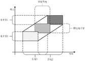
图3本发明中基于可变非对称供电机制的集成运放电平窗扩展装置的电平窗拓展示意图。在供电1情况下,电平窗移动到电平窗1;供电2情况下,电平窗移动到电平窗2。根据应用场景实时调节集成运放的电源,可以扩展集成运放电平窗。如图3所示,相比于固定供电电源,本发明的可变非对称电源供电,至少扩展集成运放的输入输出电平窗三倍以上,由电源与输入输出电平窗计算式可知,集成运放输入输出电平窗与其电源之间的关系是线性的。3 is a schematic diagram of the level window expansion of the integrated operational amplifier level window expansion device based on the variable asymmetric power supply mechanism in the present invention. In the case of power supply 1, the level window moves to level window 1; in the case of power supply 2, the level window moves to level window 2. The power supply of the integrated op amp can be adjusted in real time according to the application scenario, and the level window of the integrated op amp can be expanded. As shown in Figure 3, compared with the fixed power supply, the variable asymmetric power supply of the present invention can at least expand the input and output level window of the integrated operational amplifier by more than three times. From the calculation formula of the power supply and the input and output level window, The relationship between the input and output level window of an integrated op amp and its power supply is linear.
尽管上面对本发明说明性的具体实施方式进行了描述,以便于本技术领域的技术人员理解本发明,但应该清楚,本发明不限于具体实施方式的范围,对本技术领域的普通技术人员来讲,只要各种变化在所附的权利要求限定和确定的本发明的精神和范围内,这些变化是显而易见的,一切利用本发明构思的发明创造均在保护之列。Although the illustrative specific embodiments of the present invention have been described above to facilitate the understanding of the present invention by those skilled in the art, it should be clear that the present invention is not limited to the scope of the specific embodiments. For those skilled in the art, As long as various changes are within the spirit and scope of the present invention as defined and determined by the appended claims, these changes are obvious, and all inventions and creations utilizing the inventive concept are included in the protection list.
Claims (1)
Priority Applications (1)
| Application Number | Priority Date | Filing Date | Title |
|---|---|---|---|
| CN202110675590.8ACN113395046B (en) | 2021-06-18 | 2021-06-18 | Integrated operation and discharge flat window expanding device based on variable asymmetric power supply mechanism |
Applications Claiming Priority (1)
| Application Number | Priority Date | Filing Date | Title |
|---|---|---|---|
| CN202110675590.8ACN113395046B (en) | 2021-06-18 | 2021-06-18 | Integrated operation and discharge flat window expanding device based on variable asymmetric power supply mechanism |
Publications (2)
| Publication Number | Publication Date |
|---|---|
| CN113395046A CN113395046A (en) | 2021-09-14 |
| CN113395046Btrue CN113395046B (en) | 2022-06-03 |
Family
ID=77621905
Family Applications (1)
| Application Number | Title | Priority Date | Filing Date |
|---|---|---|---|
| CN202110675590.8AExpired - Fee RelatedCN113395046B (en) | 2021-06-18 | 2021-06-18 | Integrated operation and discharge flat window expanding device based on variable asymmetric power supply mechanism |
Country Status (1)
| Country | Link |
|---|---|
| CN (1) | CN113395046B (en) |
Citations (3)
| Publication number | Priority date | Publication date | Assignee | Title |
|---|---|---|---|---|
| CN201667616U (en)* | 2010-03-29 | 2010-12-08 | 比亚迪股份有限公司 | A multi-channel power supply load circuit |
| CN204597904U (en)* | 2015-06-11 | 2015-08-26 | 苏州索拉科技有限公司 | A kind of low-voltage discharge circuit worked under high voltage environment |
| CN207976786U (en)* | 2018-02-01 | 2018-10-16 | 深圳市芬能自动化设备有限公司 | Controllable voltage constant current source module |
Family Cites Families (1)
| Publication number | Priority date | Publication date | Assignee | Title |
|---|---|---|---|---|
| CN204928754U (en)* | 2015-09-29 | 2015-12-30 | 哈尔滨新世科技有限责任公司 | Supply circuit that floats is put to fortune |
- 2021
- 2021-06-18CNCN202110675590.8Apatent/CN113395046B/ennot_activeExpired - Fee Related
Patent Citations (3)
| Publication number | Priority date | Publication date | Assignee | Title |
|---|---|---|---|---|
| CN201667616U (en)* | 2010-03-29 | 2010-12-08 | 比亚迪股份有限公司 | A multi-channel power supply load circuit |
| CN204597904U (en)* | 2015-06-11 | 2015-08-26 | 苏州索拉科技有限公司 | A kind of low-voltage discharge circuit worked under high voltage environment |
| CN207976786U (en)* | 2018-02-01 | 2018-10-16 | 深圳市芬能自动化设备有限公司 | Controllable voltage constant current source module |
Also Published As
| Publication number | Publication date |
|---|---|
| CN113395046A (en) | 2021-09-14 |
Similar Documents
| Publication | Publication Date | Title |
|---|---|---|
| CN101339443B (en) | Broad output current scope low pressure difference linear manostat | |
| CN106406411B (en) | Low differential voltage linear voltage stabilizer circuit and power supply | |
| CN103383580B (en) | Self-adaptive low drop regulator | |
| CN109683649B (en) | Constant current circuit | |
| US20210013834A1 (en) | Inverse pseudo fully-differential amplifier having common-mode feedback control circuit | |
| CN101630944B (en) | Drive circuit for improved response speed | |
| CN205693639U (en) | A kind of Full differential operational amplifier based on feedforward with weak positive feedback | |
| CN101839941B (en) | Signal sensing amplifier | |
| CN102868295B (en) | Bootstrap type charging circuit applied to high-voltage DC-DC (Direct Current-Direct Current) convertor | |
| CN106301264A (en) | A kind of Slew Rate enhancement mode operational amplifier | |
| TW201633704A (en) | Differential amplifiers | |
| CN206627849U (en) | The CMOS low pressure difference linear voltage regulators and electronic equipment of dynamic miller compensation | |
| CN102147630A (en) | Controller and driving circuit with controller | |
| CN102722209A (en) | Constant current source circuit | |
| CN106249795A (en) | A kind of LDO circuit of output of floating | |
| CN113395046B (en) | Integrated operation and discharge flat window expanding device based on variable asymmetric power supply mechanism | |
| CN102571004A (en) | Operational amplifier | |
| CN109101069B (en) | Voltage buffer circuit | |
| CN101510724B (en) | Low voltage output circuit | |
| CN109347453A (en) | A High Linear Precision Fully Differential Operational Amplifier Circuit Structure | |
| CN104378073A (en) | Operational amplifier | |
| CN209767486U (en) | A Fast High Frequency Current Amplifier | |
| CN104320105A (en) | A mixed model capacitance multiplier circuit | |
| CN203423670U (en) | Variable-gain analog adder | |
| CN106980337A (en) | A kind of low pressure difference linear voltage regulator |
Legal Events
| Date | Code | Title | Description |
|---|---|---|---|
| PB01 | Publication | ||
| PB01 | Publication | ||
| SE01 | Entry into force of request for substantive examination | ||
| SE01 | Entry into force of request for substantive examination | ||
| GR01 | Patent grant | ||
| GR01 | Patent grant | ||
| CF01 | Termination of patent right due to non-payment of annual fee | ||
| CF01 | Termination of patent right due to non-payment of annual fee | Granted publication date:20220603 |