CN113394228B - Three-dimensional memory and preparation method thereof - Google Patents
Three-dimensional memory and preparation method thereofDownload PDFInfo
- Publication number
- CN113394228B CN113394228BCN202110628570.5ACN202110628570ACN113394228BCN 113394228 BCN113394228 BCN 113394228BCN 202110628570 ACN202110628570 ACN 202110628570ACN 113394228 BCN113394228 BCN 113394228B
- Authority
- CN
- China
- Prior art keywords
- layer
- charge trapping
- blocking
- trench
- channel hole
- Prior art date
- Legal status (The legal status is an assumption and is not a legal conclusion. Google has not performed a legal analysis and makes no representation as to the accuracy of the status listed.)
- Active
Links
Images


Classifications
- H—ELECTRICITY
- H10—SEMICONDUCTOR DEVICES; ELECTRIC SOLID-STATE DEVICES NOT OTHERWISE PROVIDED FOR
- H10B—ELECTRONIC MEMORY DEVICES
- H10B43/00—EEPROM devices comprising charge-trapping gate insulators
- H10B43/30—EEPROM devices comprising charge-trapping gate insulators characterised by the memory core region
- H10B43/35—EEPROM devices comprising charge-trapping gate insulators characterised by the memory core region with cell select transistors, e.g. NAND
- H—ELECTRICITY
- H10—SEMICONDUCTOR DEVICES; ELECTRIC SOLID-STATE DEVICES NOT OTHERWISE PROVIDED FOR
- H10B—ELECTRONIC MEMORY DEVICES
- H10B43/00—EEPROM devices comprising charge-trapping gate insulators
- H10B43/20—EEPROM devices comprising charge-trapping gate insulators characterised by three-dimensional arrangements, e.g. with cells on different height levels
- H10B43/23—EEPROM devices comprising charge-trapping gate insulators characterised by three-dimensional arrangements, e.g. with cells on different height levels with source and drain on different levels, e.g. with sloping channels
- H10B43/27—EEPROM devices comprising charge-trapping gate insulators characterised by three-dimensional arrangements, e.g. with cells on different height levels with source and drain on different levels, e.g. with sloping channels the channels comprising vertical portions, e.g. U-shaped channels
Landscapes
- Non-Volatile Memory (AREA)
- Semiconductor Memories (AREA)
Abstract
Description
Translated fromChinese技术领域technical field
本申请涉及半导体技术领域,更具体地,涉及三维储存器及其制备方法。The present application relates to the field of semiconductor technology, and more particularly, to a three-dimensional memory device and a preparation method thereof.
背景技术Background technique
三维存储器(3D NAND)中沟道结构的功能层是其实现存储功能的关键结构。具体地,功能层包括沿径向由内向外的氧化硅-氮化硅-氧化硅(ONO)结构,每个栅极层可与对应的ONO结构功能层相接触,以形成存储单元。此外,栅极层还可控制对应的ONO结构以捕获电荷的方式实现存储功能。The functional layer of the channel structure in the three-dimensional memory (3D NAND) is the key structure to realize the storage function. Specifically, the functional layer includes a silicon oxide-silicon nitride-silicon oxide (ONO) structure from the inside to the outside in a radial direction, and each gate layer can be in contact with a corresponding functional layer of the ONO structure to form a memory cell. In addition, the gate layer can also control the corresponding ONO structure to realize the storage function by trapping charges.
在现有技术中,通常采用氮化硅层作为电荷陷阱(SiN charge trap),使电荷(空穴或电子)保持在电荷捕获层中。然而,在存储过程中,存储于电荷陷阱的电荷会向沟道结构的轴向方向横向扩散(lateral spreading),这会造成栅极层对应的电荷捕获层的存储可靠性降低,从而降低三维存储器的保持(retention)特性。In the prior art, a silicon nitride layer is generally used as a charge trap (SiN charge trap) to keep charges (holes or electrons) in the charge trap layer. However, during the storage process, the charges stored in the charge traps will spread laterally in the axial direction of the channel structure, which will reduce the storage reliability of the charge trapping layer corresponding to the gate layer, thereby reducing the three-dimensional memory. The retention feature of .
因而,如何改善电荷陷阱中的电荷横向扩散,是本领域技术人员致力于解决的技术问题之一。Therefore, how to improve the lateral diffusion of charges in the charge traps is one of the technical problems to be solved by those skilled in the art.
发明内容SUMMARY OF THE INVENTION
本申请提供了一种三维存储器的制备方法。该制备方法包括:在衬底上形成包括交替叠置的电介质层和牺牲层的叠层结构,并形成贯穿所述叠层结构的沟道孔;经由沟道孔去除牺牲层的朝向沟道孔的一部分,以形成第一沟槽;在第一沟槽内依次形成阻挡层和电荷捕获层;以及在沟道孔的侧壁上形成隧穿层,以覆盖电荷捕获层和所述阻挡层。The present application provides a preparation method of a three-dimensional memory. The preparation method includes: forming a stack structure including alternately stacked dielectric layers and sacrificial layers on a substrate, and forming a channel hole penetrating the stack structure; removing the channel hole facing the sacrificial layer through the channel hole forming a first trench; forming a blocking layer and a charge trapping layer in sequence in the first trench; and forming a tunneling layer on the sidewall of the channel hole to cover the charge trapping layer and the blocking layer.
在一些实施方式中,在第一沟槽内依次形成阻挡层和电荷捕获层的步骤可包括:在第一沟槽的内壁上形成阻挡层;以及在形成有阻挡层的第一沟槽内形成电荷捕获层。In some embodiments, the step of sequentially forming the blocking layer and the charge trapping layer in the first trench may include: forming the blocking layer on the inner wall of the first trench; and forming the first trench in which the blocking layer is formed charge trapping layer.
在一些实施方式中,在第一沟槽内依次形成阻挡层和电荷捕获层的步骤可包括:在沟道孔的侧壁和第一沟槽的内壁上依次形成阻挡层和电荷捕获层;以及去除阻挡层和电荷捕获层的位于沟道孔的侧壁上的部分。In some embodiments, the step of sequentially forming the blocking layer and the charge trapping layer in the first trench may include: sequentially forming the blocking layer and the charge trapping layer on the sidewall of the channel hole and the inner wall of the first trench; and Portions of the blocking layer and the charge trapping layer on the sidewalls of the channel holes are removed.
在一些实施方式中,在第一沟槽内依次形成阻挡层和电荷捕获层的步骤还可包括:去除阻挡层的位于第一沟槽的内壁上的并且朝向沟道孔的一部分,以形成第二沟槽。In some embodiments, the step of sequentially forming the blocking layer and the charge trapping layer in the first trench may further include: removing a portion of the blocking layer located on the inner wall of the first trench and facing the channel hole to form the first trench. Two grooves.
在一些实施方式中,在沟道孔的侧壁上形成隧穿层,以覆盖电荷捕获层和阻挡层的步骤可包括:在第二沟槽内形成所述隧穿层。In some embodiments, forming a tunneling layer on the sidewall of the channel hole to cover the charge trapping layer and the blocking layer may include: forming the tunneling layer in the second trench.
在一些实施方式中,在第一沟槽内依次形成阻挡层和电荷捕获层的步骤可包括:在第一沟槽的朝向沟道孔的表面依次形成阻挡层和电荷捕获层,使得阻挡层和电荷捕获层与相邻的电介质层相接触。In some embodiments, the step of sequentially forming the blocking layer and the charge trapping layer in the first trench may include: sequentially forming the blocking layer and the charge trapping layer on the surface of the first trench facing the channel hole, so that the blocking layer and the charge trapping layer are formed sequentially. The charge trapping layer is in contact with the adjacent dielectric layer.
本申请还提供了一种三维存储器。该三维存储器包括:衬底;叠层结构,位于衬底上,包括交替叠置的电介质层和栅极层;沟道结构,贯穿叠层结构,包括:电介质芯部;围绕电介质芯部的隧穿层;以及依次位于隧穿层外侧的电荷捕获层和阻挡层;其中,电荷捕获层包括多个电荷捕获部分,阻挡层包括多个阻挡部分,电荷捕获部分和阻挡部分位于相邻的电介质层之间。The present application also provides a three-dimensional memory. The three-dimensional memory includes: a substrate; a stack structure on the substrate, including alternately stacked dielectric layers and gate layers; a channel structure, penetrating the stack structure, including: a dielectric core; a tunnel surrounding the dielectric core A pass-through layer; and a charge trapping layer and a blocking layer sequentially located outside the tunneling layer; wherein the charge trapping layer includes a plurality of charge trapping parts, the blocking layer includes a plurality of blocking parts, and the charge trapping part and the blocking part are located in adjacent dielectric layers between.
在一些实施方式中,阻挡部分可至少部分包围电荷捕获部分,隧穿层向阻挡层的方向延伸至相邻的电介质层之间,并与阻挡部分共同环绕电荷捕获部分。In some embodiments, the blocking portion may at least partially surround the charge trapping portion, and the tunneling layer extends between adjacent dielectric layers in the direction of the blocking layer and together with the blocking portion surrounds the charge trapping portion.
在一些实施方式中,电荷捕获部分和阻挡部分可沿电介质芯部的径向方向由内向外依次位于隧穿层的表面,并均与相邻的电介质层相接触。In some embodiments, the charge trapping portion and the blocking portion may be located on the surface of the tunneling layer sequentially from the inside to the outside along the radial direction of the dielectric core, and both are in contact with the adjacent dielectric layers.
在一些实施方式中,阻挡层和栅极层接触的表面可与隧穿层和电介质层接触的表面之间具有预定的距离。In some embodiments, the surface in contact with the barrier layer and the gate layer may have a predetermined distance between the surface in contact with the tunnel layer and the dielectric layer.
在一些实施方式中,阻挡层的材料可包括氧化硅,电荷捕获层的材料可包括氮化硅,隧穿层的材料可包括氧化硅。In some embodiments, the material of the blocking layer may include silicon oxide, the material of the charge trapping layer may include silicon nitride, and the material of the tunneling layer may include silicon oxide.
根据本申请实施方式的三维存储器及其制备方法,通过在牺牲层内形成沟槽以及将电荷捕获层形成于沟槽内,使电荷捕获层位于相邻的电介质层之间,能够有效地抑制栅极层对应的电荷捕获层中的电荷的横向扩散,从而提高电荷捕获层的存储可靠性,进而提高制备完成后的三维存储器的保持特性。According to the three-dimensional memory and the method for fabricating the same according to the embodiment of the present application, by forming the trench in the sacrificial layer and forming the charge trapping layer in the trench, so that the charge trapping layer is located between adjacent dielectric layers, the gate can be effectively suppressed The lateral diffusion of charges in the charge trapping layer corresponding to the polar layer improves the storage reliability of the charge trapping layer, thereby improving the retention characteristics of the three-dimensional memory after the preparation is completed.
附图说明Description of drawings
通过阅读参照以下附图所作的对非限制性实施例所作的详细描述,本申请的其它特征、目的和优点将会变得更明显:Other features, objects and advantages of the present application will become more apparent by reading the detailed description of non-limiting embodiments made with reference to the following drawings:
图1是现有的三维存储器的电荷横向扩散原理图;1 is a schematic diagram of the lateral diffusion of charges in an existing three-dimensional memory;
图2是根据本申请实施方式的三维存储器的制备方法的流程图;2 is a flowchart of a method for manufacturing a three-dimensional memory according to an embodiment of the present application;
图3A至图3F是根据本申请实施方式的三维存储器的制备方法的工艺剖面示意图;3A to 3F are process cross-sectional schematic diagrams of a method for fabricating a three-dimensional memory according to an embodiment of the present application;
图4是根据本申请另一实施方式的三维存储器的制备方法的工艺剖面示意图;以及4 is a schematic cross-sectional process diagram of a method for manufacturing a three-dimensional memory according to another embodiment of the present application; and
图5是根据申请实施方式的形成沟道结构后的剖面结构示意图;以及5 is a schematic diagram of a cross-sectional structure after forming a channel structure according to an embodiment of the application; and
图6是根据本申请实施方式的执行“栅极代替”操作后的剖面结构示意图。FIG. 6 is a schematic cross-sectional structure diagram after performing a “gate replacement” operation according to an embodiment of the present application.
具体实施方式Detailed ways
为了更好地理解本申请,将参考附图对本申请的各个方面做出更详细的说明。应理解,这些详细说明只是对本申请的示例性实施方式的描述,而非以任何方式限制本申请的范围。For a better understanding of the present application, various aspects of the present application will be described in more detail with reference to the accompanying drawings. It should be understood that these detailed descriptions are merely illustrative of exemplary embodiments of the present application and are not intended to limit the scope of the present application in any way.
本文使用的术语是为了描述特定示例性实施方式的目的,并且不意在进行限制。当在本说明书中使用时,术语“包含”、“包含有”、“包括”和/或“包括有”表示存在所述特征、整体、元件、部件和/或它们的组合,但是并不排除一个或多个其它特征、整体、元件、部件和/或它们的组合的存在性。The terminology used herein is for the purpose of describing particular example embodiments and is not intended to be limiting. When used in this specification, the terms "comprising", "comprising", "including" and/or "comprising" indicate the presence of stated features, integers, elements, parts and/or combinations thereof, but do not exclude The presence of one or more other features, integers, elements, components and/or combinations thereof.
本文参考示例性实施方式的示意图来进行描述。本文公开的示例性实施方式不应被解释为限于示出的具体形状和尺寸,而是包括能够实现相同功能的各种等效结构以及由例如制造时产生的形状和尺寸偏差。附图中所示的位置本质上是示意性的,而非旨在对各部件的位置进行限制。This document is described with reference to schematic illustrations of exemplary embodiments. The exemplary embodiments disclosed herein should not be construed as limited to the specific shapes and dimensions shown, but to include various equivalent structures capable of achieving the same function, as well as deviations in shape and dimensions resulting, for example, in manufacture. The locations shown in the figures are schematic in nature and are not intended to limit the location of the various components.
除非另有限定,否则本文使用的所有术语(包括技术术语和科学术语)具有与本公开所属技术领域的普通技术人员的通常理解相同的含义。诸如常用词典中定义的术语应被解释为具有与其在相关领域的语境下的含义一致的含义,并且将不以理想化或过度正式的意义来解释,除非本文明确地如此定义。Unless otherwise defined, all terms (including technical and scientific terms) used herein have the same meaning as commonly understood by one of ordinary skill in the art to which this disclosure belongs. Terms such as those defined in commonly used dictionaries should be construed to have meanings consistent with their meanings in the context of the relevant art, and are not to be construed in an idealized or overly formal sense unless explicitly defined as such herein.
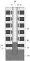
图1是现有的三维存储器的电荷横向扩散原理示意图。如图1所示,现有的三维存储器可包括沟道结构1、与沟道结构1相接触的栅极层2以及位于相邻的栅极层2之间的电介质层3。具体地,沟道结构1可包括电介质芯部4以及依次位于电介质芯部4外侧并沿着电介质芯部4的轴向方向延伸的沟道层5、隧穿层6、电荷捕获层7和阻挡层8。栅极层2可与沟道结构1中的阻挡层8相接触,并与对应的阻挡层8、电荷捕获层7、隧穿层6组成存储单元n。FIG. 1 is a schematic diagram of the principle of lateral diffusion of charges in a conventional three-dimensional memory. As shown in FIG. 1 , an existing three-dimensional memory may include a channel structure 1 , a
在对存储单元n进行编程操作时,可通过栅极层2对存储单元n施加高电压,在电场的作用下可使位于沟道层5中的电荷注入至电荷捕获层7并保持在电荷捕获层7中,从而实现存储单元n的编程。When the memory cell n is programmed, a high voltage can be applied to the memory cell n through the
然而,在对存储单元n进行编程的过程中,与存储单元n对应的栅极层2的边缘电场造成与其相邻的电介质层3位置处存在电荷注入的情况(如图1中箭头①所示的方向),从而使应注入至存储单元n内的电荷存在沿电介质芯部4的轴向方向横向扩散的情况。并且这种情况会随着施加至栅极层2的电压的增大而加剧。However, in the process of programming the memory cell n, the fringing electric field of the
另一方面,随着三维存储器的堆叠层数不断增加,为减小应力影响以及控制成本的需求,电介质层3和栅极层2的厚度也随之减薄。各个存储单元之间相互影响增强,在电荷捕获层7内沿沟道结构1的轴向方向横向扩散的现象更明显(如图1中箭头②所示的方向),从而导致三维存储器的保持特性降低。On the other hand, as the number of stacked layers of the three-dimensional memory continues to increase, the thicknesses of the
此外,现有的三维存储器在高温环境中扩散现象呈加剧的趋势。示例性地,在30℃的条件下三维存储器中的存储介质仅能够保存三个月到一年。尽管三维存储器可以通过定期刷新或者频繁备份的方式来解决存储时长的问题,然而电荷横向扩散仍然是三维存储器由于物理结构而导致的保持特性较差的技术问题之一。In addition, the diffusion phenomenon of the existing three-dimensional memory in a high temperature environment tends to intensify. Exemplarily, the storage medium in the three-dimensional memory can only be stored for three months to one year under the condition of 30°C. Although 3D memory can solve the problem of storage time by means of regular refresh or frequent backup, lateral charge diffusion is still one of the technical problems of poor retention characteristics of 3D memory due to its physical structure.
基于上述技术问题,本申请提供了一种三维存储器的制备方法1000。图2是根据本申请实施方式的三维存储器的制备方法1000的流程图。如图2所示,三维存储器的制备方法1000包括如下步骤。Based on the above technical problems, the present application provides a
S110,在衬底上形成包括交替叠置的电介质层和牺牲层的叠层结构,并形成贯穿叠层结构的沟道孔。S110 , forming a stack structure including alternately stacked dielectric layers and sacrificial layers on the substrate, and forming a channel hole penetrating the stack structure.
S120,经由沟道孔去除牺牲层的朝向沟道孔的一部分,以形成第一沟槽。S120, a part of the sacrificial layer facing the channel hole is removed through the channel hole to form a first trench.
S130,在第一沟槽内依次形成阻挡层和电荷捕获层。S130, forming a blocking layer and a charge trapping layer in sequence in the first trench.
S140,在沟道孔的侧壁上形成隧穿层,以覆盖电荷捕获层和阻挡层。S140, forming a tunneling layer on the sidewall of the channel hole to cover the charge trapping layer and the blocking layer.
图3A至图3F是根据本申请实施方式的三维存储器的制备方法1000的工艺剖面示意图。其中,图3B至图3F为图3A中区域A的局部放大图。应理解的是,制备方法1000中所示的步骤不是排它性的,还可以在所示步骤中的任何步骤之前、之后或之间执行其它步骤。此外,所述步骤中的一些步骤可以是同时地执行的或者可以是按照不同于图2所示的顺序执行的。下面将结合图3A至图3F详细地描述上述的步骤S110至步骤S140。3A to 3F are schematic cross-sectional process diagrams of a
S110,在衬底上形成包括交替叠置的电介质层和牺牲层的叠层结构,并形成贯穿S110, forming a stack structure including alternately stacked dielectric layers and sacrificial layers on the substrate, and forming a through叠层结构的沟道孔。The channel hole of the stack structure.
在步骤S110中,如图3A所示,衬底10可用于支撑其上的器件结构。衬底10可为单晶硅(Si)衬底、单晶锗(Ge)衬底、绝缘体上硅(SOI)衬底或者绝缘体上锗(GOI)衬底等。衬底10的材料还可为化合物半导体。举例而言,衬底10可为砷化镓(GaAs)衬底、磷化铟(InP)衬底或碳化硅(SiC)衬底等。值得注意的是,本申请所述的衬底10还可采用本领域中已知的其它半导体材料中的至少一种制备。此外,衬底10还可为掺杂有P型或者N型掺杂剂的半导体衬底。In step S110, as shown in FIG. 3A, the
叠层结构20可包括在垂直于衬底10的方向上交叠叠置的多个电介质层21和多个牺牲层22。叠层结构20的形成方法可包括诸如化学气相沉积(CVD)、物理气相沉积(PVD)、原子层沉积(ALD)或其任何组合的薄膜沉积工艺。在叠层结构20中,多个电介质层21的厚度可相同也可不相同,多个牺牲层22的厚度可相同也可不相同,并且可根据具体工艺需求进行设置。此外,在叠层结构20的生产工艺中,不同的堆叠层数会对应不同的堆叠高度,举例而言,叠层结构20堆叠的层数可为8层、32层、64层、128层等,叠层结构20的层数越多,集成度越高,由其形成的存储单元的个数越多,可根据实际存储需求来设计叠层结构20的堆叠层数及堆叠高度,本申请对此不做具体的限定。The stacked
在一些实施方式中,电介质层21和牺牲层22可具有不同的刻蚀选择比,牺牲层22可在后续的工艺过程中被去除并被导电材料代替,从而形成栅极层即字线。可选地,电介质层21的材料可包括氧化硅,牺牲层22的材料可包括氮化硅。In some embodiments, the
在该步骤中,可采用例如湿法刻蚀工艺或者诸如等离子体刻蚀、离子铣刻蚀以及反应离子刻蚀等干法刻蚀工艺形成垂直地贯穿叠层结构20的沟道孔31,并且沟道孔31可延伸至衬底10,从而暴露衬底10。In this step, for example, a wet etching process or a dry etching process such as plasma etching, ion milling etching, and reactive ion etching may be used to form the
S120,经由沟道孔去除牺牲层的朝向沟道孔的一部分,以形成第一沟槽。S120, a part of the sacrificial layer facing the channel hole is removed through the channel hole to form a first trench.
在步骤S120中,如图3B所示,可利用上述步骤S110中形成的沟道孔31,采用例如湿法刻蚀工艺或者诸如等离子体刻蚀、离子铣刻蚀以及反应离子刻蚀等干法刻蚀工艺去除牺牲层22朝向沟道孔31的一部分,从而形成第一沟槽23。第一沟槽23可由相邻的电介质层21的表面和位于相邻的电介质层21之间的牺牲层22的表面构成。In step S120, as shown in FIG. 3B, the
在一些实施方式中,第一沟槽23朝向沟道孔31的表面可与沟道孔31的侧壁具有预定的距离,例如20nm。第一沟道23可用于容置在后续工艺过程中形成的阻挡层和电荷捕获层。In some embodiments, the surface of the
S130,在第一沟槽内依次形成阻挡层和电荷捕获层。S130, forming a blocking layer and a charge trapping layer in sequence in the first trench.
在步骤S130中,可采用诸如CVD、PVD、ALD或其任何组合的薄膜沉积工艺在第一沟槽23内沿着朝向沟道孔的方向依次形成阻挡层和电荷捕获层,从而使电荷捕获层形成于叠层结构20中相邻的电介质层21之间。可以理解的是,电荷捕获层作为存储电荷的结构,将其形成于相邻的电介质层21之间有利于防止存储于其内部的电荷沿沟道孔31的轴向方向横向扩散。In step S130, a thin film deposition process such as CVD, PVD, ALD or any combination thereof may be used to sequentially form a blocking layer and a charge trapping layer in the
在一些实施方式中,形成阻挡层和电荷捕获层的步骤可包括:在第一沟槽23的内壁上形成阻挡层以及在形成有阻挡层的第一沟槽23内形成电荷捕获层。In some embodiments, the forming of the blocking layer and the charge trapping layer may include forming a blocking layer on inner walls of the
在在第一沟槽23的内壁上形成阻挡层的步骤中,如图3C所示,可采用诸如CVD、PVD、ALD或其任何组合的薄膜沉积工艺在第一沟槽23的内壁上形成阻挡层32。阻挡层32可例如选用氧化硅(SiOx)制备。可选地,在第一沟槽23的内壁上形成阻挡层32的工艺过程中,可采用相同的工艺方法在沟道孔31的侧壁上形成阻挡层32,从而形成覆盖第一沟槽23的内壁和沟道孔31的侧壁的连续层结构。In the step of forming the barrier layer on the inner wall of the
在在形成有阻挡层32的第一沟槽23内形成电荷捕获层的步骤中,如图3D所示,可采用诸如CVD、PVD、ALD或其任何组合的薄膜沉积工艺在形成有阻挡层32的第一沟槽23内形成电荷捕获层33。电荷捕获层33可例如选用氮化硅(SiNx)制备。可选地,在第一沟槽23内形成电荷捕获层33的工艺过程中,可采用相同的工艺方法在沟道层31的侧壁上形成有阻挡层32的表面进一步地形成电荷捕获层33,从而使填充于第一沟槽23内和位于沟道孔31侧壁上的电荷捕获层33具有连续层结构。In the step of forming the charge trapping layer in the
在一些实施方式中,如图3E所示,当阻挡层32和电荷捕获层33依次形成于沟道孔31的侧壁上之后,可采用例如干法或者湿法刻蚀工艺去除阻挡层32和电荷捕获层33的位于沟道孔31的侧壁上的部分,从而确保电荷捕获层33位于相邻的电介质层21之间。可选地,还可采用相同的工艺方法,在去除阻挡层32和电荷捕获层33的位于沟道孔31的侧壁上的部分的同时,去除阻挡层32的位于第一沟槽23的内壁上的并且朝向沟道孔31的一部分,从而形成电介质层21、阻挡层32以及电荷捕获层33的表面构成的第二沟槽24。第二沟槽24可包括靠近相邻的电介质层21的两个部分。In some embodiments, as shown in FIG. 3E , after the
S140,在沟道孔的侧壁上形成隧穿层,以覆盖电荷捕获层和阻挡层。S140, forming a tunneling layer on the sidewall of the channel hole to cover the charge trapping layer and the blocking layer.
在步骤S140中,如图3F所示,可采用诸如CVD、PVD、ALD或其任何组合的薄膜沉积工艺在沟道孔31的侧壁上形成隧穿层34,从而覆盖形成于第一沟槽23内的阻挡层32和电荷捕获层33。隧穿层34的材料可例如选用氧化硅(SiOx)制备。此外,隧穿层34还可与电荷捕获层33相接触,并与形成于第一沟槽23内的阻挡层32和电荷捕获层33共同组成后续工艺过程中形成的沟道结构的用于实现存储功能的功能层。In step S140, as shown in FIG. 3F, a thin film deposition process such as CVD, PVD, ALD or any combination thereof may be used to form a
在一些实施方式中,在沟道孔31的侧壁上形成隧穿层34的工艺过程中,可采用相同的工艺方法,在步骤S130中形成的第二沟槽24内形成隧穿层34。换言之,隧穿层34可延伸至相邻的电介质层21之间,并与阻挡层32共同环绕电荷捕获层33。应当理解的是,可采用刻蚀工艺去除隧穿层34与电介质层21对应的部分,以使隧穿层34保留在沟道孔的侧壁上并与牺牲层22对应,从而使隧穿层34形成位于沟道孔的侧壁上的离散的层结构。In some embodiments, during the process of forming the
图4是根据本申请另一实施方式的三维存储器的制备方法的工艺剖面示意图。如图4所示,可采用诸如CVD、PVD、ALD或其任何组合的薄膜沉积工艺在第一沟槽23的朝向沟道孔31的表面依次形成阻挡层32和电荷捕获层33,使得阻挡层32与牺牲层22以及相邻的电介质层21相接触,并且使得电荷捕获层33与阻挡层32以及相邻的电介质层21相接触。经上述工艺处理后,电荷捕获层33的朝向沟道孔31的表面可与沟道孔31的侧壁平齐,从而隧穿层34形成于沟道孔31的侧壁上。可选地,电荷捕获层33的朝向沟道孔31的表面可与沟道孔31的侧壁具有预定的距离。换言之,电荷捕获层33可与相邻的电介质层21形成沟槽,从而使隧穿层34在形成于沟道孔31的侧壁上的同时进一步地延伸至沟槽内,并与电荷捕获层33以及相邻的电介质层21相接触。作为一种选择,可采用将牺牲层22的一部分氧化处理,以使氧化处理的部分牺牲层22形成阻挡层32。FIG. 4 is a process cross-sectional schematic diagram of a method for fabricating a three-dimensional memory according to another embodiment of the present application. As shown in FIG. 4 , a thin film deposition process such as CVD, PVD, ALD or any combination thereof may be used to sequentially form a
在一些实施方式中,本申请实施方式提供的三维存储器的制备方法1000还可包括形成沟道结构的步骤。图5是根据申请实施方式的形成沟道结构后的剖面结构示意图。In some embodiments, the
在该步骤中,如图5所示,在采用上述工艺方法1000形成由阻挡层32、电荷捕获层33以及隧穿层34组成的功能层的步骤之前,可采用例如选择性外延生长(SEG)工艺在沟道孔31的底部形成外延层35,外延层35可覆盖在形成沟道孔31的步骤中暴露的衬底10的预先形成的有源区,并且外延层35可与至少一个牺牲层22相对应。外延层35可与其对应的牺牲层22形成沟道结构30的底部选择晶体管。此外,外延层35可形成沟道层36和衬底10之间的电耦合区域。应当理解的是,在采用选择性外延生长工艺使沟道层36与衬底10形成电路回路的情况下,衬底10可为P型衬底。此外,衬底10还可为N型衬底或者复合衬底结构,并且使沟道结构30中的沟道层36与衬底10形成电路回路的工艺过程本申请不做具体地限定。In this step, as shown in FIG. 5 , before the step of forming the functional layer composed of the
进一步地,可采用上述工艺方法1000形成的由阻挡层32、电荷捕获层33以及隧穿层34组成的功能层,并且该功能层可还形成于外延层35的远离衬底10的表面。Further, the functional layer composed of the
进一步地,可采用例如干法或者湿法刻蚀工艺去除该功能层的位于外延层35的远离衬底10的表面的一部分,以形成暴露外延层35的开口。可选地,在去除该功能层的位于外延层35的远离衬底10的表面的一部分的工艺过程中,还可使该开口进一步地延伸至外延层35内部。Further, a part of the functional layer located on the surface of the
进一步地,可采用诸如CVD、PVD、ALD或其任何组合薄膜沉积工艺在上述步骤中形成的开口处以及沟道孔31内的隧穿层34的表面形成沟道层36。沟道层36的材料可选用多晶硅制备。应理解的是,沟道层36的材料不限于此,还可采用其它导电材料制备。Further, a thin film deposition process such as CVD, PVD, ALD or any combination thereof may be used to form the
进一步地,可采用诸如CVD、PVD、ALD或其任何组合薄膜沉积工艺在沟道孔31内填充电介质材料例如氧化硅(SiOx),以形成沟道结构30。可选地,可通过控制填充工艺,在填充过程中形成一个或多个空气间隙以减轻结构应力。Further, a thin film deposition process such as CVD, PVD, ALD, or any combination thereof may be employed to fill the
在一些实施方式中,可采用例如干法或者湿法刻蚀工艺对填充于沟道孔31内的电介质材料的远离衬底10的部分回刻,并填充导电材料,从而形成与沟道层36相接触的沟道插塞(未示出)。沟道插塞可选用与沟道层36相同的材料例如多晶硅制备,并且沟道插塞可作为沟道结构30的漏极端。In some embodiments, a portion of the dielectric material filled in the
在一些实施方式中,本申请实施方式提供的三维存储器的制备方法1000还可包括执行“栅极代替”操作的步骤。图6是根据本申请实施方式的执行“栅极代替”操作后的剖面结构示意图。In some embodiments, the
在该步骤中,如图6所示,可采用例如干法或者湿法刻蚀工艺形成贯穿叠层结构20并延伸至衬底10的栅极缝隙(未示出)。进一步地,可利用上述工艺处理后形成的栅极缝隙作为刻蚀剂的通道,采用例如湿法刻蚀工艺去除叠层结构20中的牺牲层22,以形成多个牺牲间隙。进一步地,可采用诸如CVD、PVD、ALD或其任何组合等薄膜沉积工艺在牺牲间隙内填充导电材料而形成栅极层24。栅极层24可选用诸如钨、钴、铜、铝或者掺杂的晶体硅等制备。经上述工艺处理后,叠层结构20中的牺牲层22可被替换为栅极层24。栅极层24与沟道结构30相接触。更具体地,栅极层24可与沟道结构30中的阻挡层32相接触,并控制沟道结构30中包括阻挡层32、电荷捕获层33以及隧穿层34共同组成的存储单元,从而使存储单元中电荷捕获层33能够以保持电荷的方式处于存储状态。In this step, as shown in FIG. 6 , a gate slit (not shown) extending through the stacked
本申请提供的三维存储器的制备方法,通过在牺牲层内形成沟槽以及将电荷捕获层形成于沟槽内,使电荷捕获层位于相邻的电介质层之间,能够有效地抑制栅极层对应的电荷捕获层中电荷的横向扩散,从而提高电荷捕获层的存储可靠性,进而提高制备完成后的三维存储器的保持特性。In the method for preparing a three-dimensional memory provided by the present application, by forming a trench in a sacrificial layer and forming a charge trapping layer in the trench, so that the charge trapping layer is located between adjacent dielectric layers, the corresponding gate layer can be effectively suppressed. The lateral diffusion of charges in the charge trapping layer can improve the storage reliability of the charge trapping layer, thereby improving the retention characteristics of the three-dimensional memory after the preparation is completed.
本申请还提供了一种三维存储器。该三维存储器可采用上述实施方式中任一制备方法获得。该三维存储器可包括:衬底、叠层结构和沟道结构。The present application also provides a three-dimensional memory. The three-dimensional memory can be obtained by using any of the preparation methods in the above-mentioned embodiments. The three-dimensional memory may include: a substrate, a stack structure, and a channel structure.
叠层结构位于衬底上,并包括交替叠置的电介质层和栅极层。沟道结构贯穿该叠层结构。沟道结构包括:电介质芯部、围绕电介质芯部的隧穿层以及依次位于隧穿层外侧的电荷捕获层和阻挡层。其中,电荷捕获层包括多个电荷捕获部分,阻挡层包括多个阻挡部分,电荷捕获部分和阻挡部分位于相邻的电介质层之间,使得电荷捕获部分被相邻的电介质层间隔,从而能够有效地抑制栅极层对应的电荷捕获部分中电荷的横向扩散,进而提高电荷捕获层的存储可靠性。同时,能够提高三维存储器的保持特性。The stacked structure is on the substrate and includes alternately stacked dielectric layers and gate layers. A channel structure penetrates the stacked structure. The channel structure includes: a dielectric core, a tunneling layer surrounding the dielectric core, and a charge trapping layer and a blocking layer sequentially located outside the tunneling layer. The charge trapping layer includes a plurality of charge trapping portions, the blocking layer includes a plurality of blocking portions, and the charge trapping portion and the blocking portion are located between adjacent dielectric layers, so that the charge trapping portions are separated by the adjacent dielectric layers, thereby effectively The lateral diffusion of charges in the charge trapping portion corresponding to the gate layer is effectively suppressed, thereby improving the storage reliability of the charge trapping layer. At the same time, the retention characteristics of the three-dimensional memory can be improved.
由于在上文中描述制备方法1000时涉及的内容和结构可完全或部分地适用于在这里描述的三维存储器,因此与其相关或相似的内容不再赘述。Since the contents and structures involved in the above description of the
以上描述仅为本申请的较佳实施方式以及对所运用技术原理的说明。本领域技术人员应当理解,本申请中所涉及的发明范围,并不限于上述技术特征的特定组合而成的技术方案,同时也应涵盖在不脱离所述发明构思的情况下,由上述技术特征或其等同特征进行任意组合而形成的其它技术方案。例如上述特征与本申请中公开的(但不限于)具有类似功能的技术特征进行互相替换而形成的技术方案。The above description is only a preferred embodiment of the present application and an illustration of the applied technical principles. Those skilled in the art should understand that the scope of the invention involved in this application is not limited to the technical solution formed by the specific combination of the above-mentioned technical features, and should also cover the above-mentioned technical features without departing from the inventive concept. Other technical solutions formed by any combination of its equivalent features. For example, a technical solution is formed by replacing the above-mentioned features with the technical features disclosed in this application (but not limited to) with similar functions.
Claims (8)
Translated fromChinesePriority Applications (8)
| Application Number | Priority Date | Filing Date | Title |
|---|---|---|---|
| CN202110628570.5ACN113394228B (en) | 2021-06-07 | 2021-06-07 | Three-dimensional memory and preparation method thereof |
| CN202180003163.3ACN113924647B (en) | 2020-10-19 | 2021-08-31 | Three-dimensional memory device and method for forming the three-dimensional memory device |
| CN202180003162.9ACN113924646A (en) | 2020-10-19 | 2021-08-31 | Three-dimensional memory device and method for forming the same |
| PCT/CN2021/115782WO2022083298A1 (en) | 2020-10-19 | 2021-08-31 | Three-dimensional memory device and method for forming the same |
| PCT/CN2021/115807WO2022083299A1 (en) | 2020-10-19 | 2021-08-31 | Three-dimensional memory device and method for forming the same |
| US17/488,879US12171098B2 (en) | 2020-10-19 | 2021-09-29 | Three-dimensional memory device with improved charge lateral migration and method for forming the same |
| US17/488,915US12193233B2 (en) | 2020-10-19 | 2021-09-29 | Three-dimensional memory device with restrained charge migration and method for forming the same |
| US18/931,775US20250056804A1 (en) | 2020-10-19 | 2024-10-30 | Three-dimensional memory device with improved charge lateral migration and method for forming the same |
Applications Claiming Priority (1)
| Application Number | Priority Date | Filing Date | Title |
|---|---|---|---|
| CN202110628570.5ACN113394228B (en) | 2021-06-07 | 2021-06-07 | Three-dimensional memory and preparation method thereof |
Publications (2)
| Publication Number | Publication Date |
|---|---|
| CN113394228A CN113394228A (en) | 2021-09-14 |
| CN113394228Btrue CN113394228B (en) | 2022-05-20 |
Family
ID=77618387
Family Applications (1)
| Application Number | Title | Priority Date | Filing Date |
|---|---|---|---|
| CN202110628570.5AActiveCN113394228B (en) | 2020-10-19 | 2021-06-07 | Three-dimensional memory and preparation method thereof |
Country Status (1)
| Country | Link |
|---|---|
| CN (1) | CN113394228B (en) |
Families Citing this family (1)
| Publication number | Priority date | Publication date | Assignee | Title |
|---|---|---|---|---|
| CN114613839A (en)* | 2022-03-01 | 2022-06-10 | 长江存储科技有限责任公司 | Method for manufacturing three-dimensional memory and three-dimensional memory |
Citations (4)
| Publication number | Priority date | Publication date | Assignee | Title |
|---|---|---|---|---|
| CN105723511A (en)* | 2013-12-24 | 2016-06-29 | 英特尔公司 | Memory strucutre with self-aligned floating and control gates and associated methods |
| US20180374863A1 (en)* | 2017-06-26 | 2018-12-27 | Applied Materials, Inc. | 3d flash memory cells which discourage cross-cell electrical tunneling |
| CN111987106A (en)* | 2020-08-24 | 2020-11-24 | 维沃移动通信有限公司 | Memory and method of making the same |
| US20210066346A1 (en)* | 2019-09-03 | 2021-03-04 | Samsung Electronics Co., Ltd. | Semiconductor devices including separate charge storage layers |
Family Cites Families (3)
| Publication number | Priority date | Publication date | Assignee | Title |
|---|---|---|---|---|
| US8946807B2 (en)* | 2013-01-24 | 2015-02-03 | Micron Technology, Inc. | 3D memory |
| US10680009B2 (en)* | 2017-08-23 | 2020-06-09 | Yangtze Memory Technologies Co., Ltd. | Method for forming gate structure of three-dimensional memory device |
| CN112640103B (en)* | 2020-11-10 | 2023-10-17 | 长江存储科技有限责任公司 | Channel structure with protruding portion in three-dimensional memory device and method for forming same |
- 2021
- 2021-06-07CNCN202110628570.5Apatent/CN113394228B/enactiveActive
Patent Citations (4)
| Publication number | Priority date | Publication date | Assignee | Title |
|---|---|---|---|---|
| CN105723511A (en)* | 2013-12-24 | 2016-06-29 | 英特尔公司 | Memory strucutre with self-aligned floating and control gates and associated methods |
| US20180374863A1 (en)* | 2017-06-26 | 2018-12-27 | Applied Materials, Inc. | 3d flash memory cells which discourage cross-cell electrical tunneling |
| US20210066346A1 (en)* | 2019-09-03 | 2021-03-04 | Samsung Electronics Co., Ltd. | Semiconductor devices including separate charge storage layers |
| CN111987106A (en)* | 2020-08-24 | 2020-11-24 | 维沃移动通信有限公司 | Memory and method of making the same |
Also Published As
| Publication number | Publication date |
|---|---|
| CN113394228A (en) | 2021-09-14 |
Similar Documents
| Publication | Publication Date | Title |
|---|---|---|
| JP7322158B2 (en) | Three-dimensional memory device and manufacturing method thereof | |
| CN114420702A (en) | Three-dimensional memory and preparation method thereof | |
| CN111564442B (en) | Semiconductor structure and preparation method | |
| CN112820736A (en) | Three-dimensional memory and preparation method thereof | |
| CN113035884B (en) | Three-dimensional memory and preparation method thereof | |
| CN113206105B (en) | Three-dimensional memory and preparation method thereof | |
| US11411024B2 (en) | Vertical type semiconductor devices and methods of manufacturing the same | |
| CN112530975B (en) | Three-dimensional memory and preparation method thereof | |
| CN112838097A (en) | Three-dimensional memory and preparation method thereof | |
| CN110718501B (en) | Gap filling method and method for manufacturing semiconductor device using the same | |
| CN113410251B (en) | Three-dimensional memory and preparation method thereof | |
| WO2023133966A1 (en) | Method for manufacturing semiconductor structure, and semiconductor structure | |
| TWI841221B (en) | Semiconductor device | |
| WO2023029036A1 (en) | Three-dimensional memory and manufacturing method therefor | |
| CN111373538A (en) | Three-dimensional memory device and manufacturing method thereof | |
| CN117276327A (en) | Semiconductor device with a semiconductor element having a plurality of electrodes | |
| CN113394228B (en) | Three-dimensional memory and preparation method thereof | |
| CN114497057A (en) | Three-dimensional memory and preparation method thereof | |
| CN113948525A (en) | Manufacturing method of storage structure, three-dimensional memory and manufacturing method thereof | |
| TWI728815B (en) | Three-dimensional memory components and method for forong the same | |
| CN110061008B (en) | 3D NAND flash memory and preparation method thereof | |
| CN112687700A (en) | Three-dimensional memory and preparation method thereof | |
| CN112992910B (en) | Three-dimensional memory and preparation method thereof | |
| CN112864170A (en) | Three-dimensional memory and preparation method thereof | |
| CN114639682A (en) | Three-dimensional memory, preparation method and storage system |
Legal Events
| Date | Code | Title | Description |
|---|---|---|---|
| PB01 | Publication | ||
| PB01 | Publication | ||
| SE01 | Entry into force of request for substantive examination | ||
| SE01 | Entry into force of request for substantive examination | ||
| GR01 | Patent grant | ||
| GR01 | Patent grant |