CN113394166B - Manufacturing method of array substrate, array substrate and display panel - Google Patents
Manufacturing method of array substrate, array substrate and display panelDownload PDFInfo
- Publication number
- CN113394166B CN113394166BCN202110662463.4ACN202110662463ACN113394166BCN 113394166 BCN113394166 BCN 113394166BCN 202110662463 ACN202110662463 ACN 202110662463ACN 113394166 BCN113394166 BCN 113394166B
- Authority
- CN
- China
- Prior art keywords
- electrode
- layer
- additional
- via hole
- array substrate
- Prior art date
- Legal status (The legal status is an assumption and is not a legal conclusion. Google has not performed a legal analysis and makes no representation as to the accuracy of the status listed.)
- Active
Links
- 239000000758substrateSubstances0.000titleclaimsabstractdescription135
- 238000004519manufacturing processMethods0.000titleclaimsabstractdescription26
- 238000002161passivationMethods0.000claimsabstractdescription60
- 229920002120photoresistant polymerPolymers0.000claimsdescription61
- 239000004020conductorSubstances0.000claimsdescription44
- 238000000034methodMethods0.000claimsdescription24
- 238000005530etchingMethods0.000claimsdescription20
- 238000000151depositionMethods0.000claimsdescription8
- 239000004973liquid crystal related substanceSubstances0.000claimsdescription8
- 239000000126substanceSubstances0.000claimsdescription2
- 238000003860storageMethods0.000abstractdescription43
- 239000003990capacitorSubstances0.000abstractdescription29
- 238000005516engineering processMethods0.000abstractdescription2
- 239000000463materialSubstances0.000description23
- 229910052751metalInorganic materials0.000description20
- 239000002184metalSubstances0.000description20
- 238000001039wet etchingMethods0.000description17
- 238000010586diagramMethods0.000description11
- 239000011810insulating materialSubstances0.000description9
- 230000008569processEffects0.000description9
- VYPSYNLAJGMNEJ-UHFFFAOYSA-NSilicium dioxideChemical compoundO=[Si]=OVYPSYNLAJGMNEJ-UHFFFAOYSA-N0.000description8
- XLOMVQKBTHCTTD-UHFFFAOYSA-NZinc monoxideChemical compound[Zn]=OXLOMVQKBTHCTTD-UHFFFAOYSA-N0.000description8
- GPBUGPUPKAGMDK-UHFFFAOYSA-NazanylidynemolybdenumChemical compound[Mo]#NGPBUGPUPKAGMDK-UHFFFAOYSA-N0.000description8
- 229910052750molybdenumInorganic materials0.000description8
- 229910052814silicon oxideInorganic materials0.000description8
- 239000011651chromiumSubstances0.000description7
- 239000010949copperSubstances0.000description7
- 239000010936titaniumSubstances0.000description7
- 229910052581Si3N4Inorganic materials0.000description6
- 229910052782aluminiumInorganic materials0.000description6
- 229910052804chromiumInorganic materials0.000description6
- 229910052802copperInorganic materials0.000description6
- 230000001681protective effectEffects0.000description6
- 239000004065semiconductorSubstances0.000description6
- HQVNEWCFYHHQES-UHFFFAOYSA-Nsilicon nitrideChemical compoundN12[Si]34N5[Si]62N3[Si]51N64HQVNEWCFYHHQES-UHFFFAOYSA-N0.000description6
- 229910052719titaniumInorganic materials0.000description6
- XUIMIQQOPSSXEZ-UHFFFAOYSA-NSiliconChemical compound[Si]XUIMIQQOPSSXEZ-UHFFFAOYSA-N0.000description4
- GWEVSGVZZGPLCZ-UHFFFAOYSA-NTitan oxideChemical compoundO=[Ti]=OGWEVSGVZZGPLCZ-UHFFFAOYSA-N0.000description4
- 230000009286beneficial effectEffects0.000description4
- 230000008901benefitEffects0.000description4
- 230000000694effectsEffects0.000description4
- TWNQGVIAIRXVLR-UHFFFAOYSA-Noxo(oxoalumanyloxy)alumaneChemical compoundO=[Al]O[Al]=OTWNQGVIAIRXVLR-UHFFFAOYSA-N0.000description4
- 229910052710siliconInorganic materials0.000description4
- 239000010703siliconSubstances0.000description4
- OGIDPMRJRNCKJF-UHFFFAOYSA-Ntitanium oxideInorganic materials[Ti]=OOGIDPMRJRNCKJF-UHFFFAOYSA-N0.000description4
- 239000011787zinc oxideSubstances0.000description4
- 229910021417amorphous siliconInorganic materials0.000description3
- 239000011159matrix materialSubstances0.000description3
- 229910021419crystalline siliconInorganic materials0.000description2
- 238000001312dry etchingMethods0.000description2
- AMGQUBHHOARCQH-UHFFFAOYSA-Nindium;oxotinChemical compound[In].[Sn]=OAMGQUBHHOARCQH-UHFFFAOYSA-N0.000description2
- 239000010409thin filmSubstances0.000description2
- VYZAMTAEIAYCRO-UHFFFAOYSA-NChromiumChemical compound[Cr]VYZAMTAEIAYCRO-UHFFFAOYSA-N0.000description1
- RYGMFSIKBFXOCR-UHFFFAOYSA-NCopperChemical compound[Cu]RYGMFSIKBFXOCR-UHFFFAOYSA-N0.000description1
- ZOKXTWBITQBERF-UHFFFAOYSA-NMolybdenumChemical compound[Mo]ZOKXTWBITQBERF-UHFFFAOYSA-N0.000description1
- RTAQQCXQSZGOHL-UHFFFAOYSA-NTitaniumChemical compound[Ti]RTAQQCXQSZGOHL-UHFFFAOYSA-N0.000description1
- 230000005856abnormalityEffects0.000description1
- 239000002253acidSubstances0.000description1
- 230000009471actionEffects0.000description1
- XAGFODPZIPBFFR-UHFFFAOYSA-NaluminiumChemical compound[Al]XAGFODPZIPBFFR-UHFFFAOYSA-N0.000description1
- JYMITAMFTJDTAE-UHFFFAOYSA-Naluminum zinc oxygen(2-)Chemical compound[O-2].[Al+3].[Zn+2]JYMITAMFTJDTAE-UHFFFAOYSA-N0.000description1
- 238000005229chemical vapour depositionMethods0.000description1
- 230000008021depositionEffects0.000description1
- JAONJTDQXUSBGG-UHFFFAOYSA-Ndialuminum;dizinc;oxygen(2-)Chemical compound[O-2].[O-2].[O-2].[O-2].[O-2].[Al+3].[Al+3].[Zn+2].[Zn+2]JAONJTDQXUSBGG-UHFFFAOYSA-N0.000description1
- 238000009792diffusion processMethods0.000description1
- 238000005265energy consumptionMethods0.000description1
- 239000011521glassSubstances0.000description1
- 150000002500ionsChemical class0.000description1
- 239000000203mixtureSubstances0.000description1
- 238000012986modificationMethods0.000description1
- 230000004048modificationEffects0.000description1
- 239000011733molybdenumSubstances0.000description1
- 230000005855radiationEffects0.000description1
- 230000000717retained effectEffects0.000description1
Images


Classifications
- H—ELECTRICITY
- H10—SEMICONDUCTOR DEVICES; ELECTRIC SOLID-STATE DEVICES NOT OTHERWISE PROVIDED FOR
- H10D—INORGANIC ELECTRIC SEMICONDUCTOR DEVICES
- H10D86/00—Integrated devices formed in or on insulating or conducting substrates, e.g. formed in silicon-on-insulator [SOI] substrates or on stainless steel or glass substrates
- H10D86/01—Manufacture or treatment
- H10D86/021—Manufacture or treatment of multiple TFTs
- G—PHYSICS
- G02—OPTICS
- G02F—OPTICAL DEVICES OR ARRANGEMENTS FOR THE CONTROL OF LIGHT BY MODIFICATION OF THE OPTICAL PROPERTIES OF THE MEDIA OF THE ELEMENTS INVOLVED THEREIN; NON-LINEAR OPTICS; FREQUENCY-CHANGING OF LIGHT; OPTICAL LOGIC ELEMENTS; OPTICAL ANALOGUE/DIGITAL CONVERTERS
- G02F1/00—Devices or arrangements for the control of the intensity, colour, phase, polarisation or direction of light arriving from an independent light source, e.g. switching, gating or modulating; Non-linear optics
- G02F1/01—Devices or arrangements for the control of the intensity, colour, phase, polarisation or direction of light arriving from an independent light source, e.g. switching, gating or modulating; Non-linear optics for the control of the intensity, phase, polarisation or colour
- G02F1/13—Devices or arrangements for the control of the intensity, colour, phase, polarisation or direction of light arriving from an independent light source, e.g. switching, gating or modulating; Non-linear optics for the control of the intensity, phase, polarisation or colour based on liquid crystals, e.g. single liquid crystal display cells
- G02F1/133—Constructional arrangements; Operation of liquid crystal cells; Circuit arrangements
- G02F1/136—Liquid crystal cells structurally associated with a semi-conducting layer or substrate, e.g. cells forming part of an integrated circuit
- G02F1/1362—Active matrix addressed cells
- G02F1/136213—Storage capacitors associated with the pixel electrode
- G—PHYSICS
- G02—OPTICS
- G02F—OPTICAL DEVICES OR ARRANGEMENTS FOR THE CONTROL OF LIGHT BY MODIFICATION OF THE OPTICAL PROPERTIES OF THE MEDIA OF THE ELEMENTS INVOLVED THEREIN; NON-LINEAR OPTICS; FREQUENCY-CHANGING OF LIGHT; OPTICAL LOGIC ELEMENTS; OPTICAL ANALOGUE/DIGITAL CONVERTERS
- G02F1/00—Devices or arrangements for the control of the intensity, colour, phase, polarisation or direction of light arriving from an independent light source, e.g. switching, gating or modulating; Non-linear optics
- G02F1/01—Devices or arrangements for the control of the intensity, colour, phase, polarisation or direction of light arriving from an independent light source, e.g. switching, gating or modulating; Non-linear optics for the control of the intensity, phase, polarisation or colour
- G02F1/13—Devices or arrangements for the control of the intensity, colour, phase, polarisation or direction of light arriving from an independent light source, e.g. switching, gating or modulating; Non-linear optics for the control of the intensity, phase, polarisation or colour based on liquid crystals, e.g. single liquid crystal display cells
- G02F1/133—Constructional arrangements; Operation of liquid crystal cells; Circuit arrangements
- G02F1/136—Liquid crystal cells structurally associated with a semi-conducting layer or substrate, e.g. cells forming part of an integrated circuit
- G02F1/1362—Active matrix addressed cells
- G02F1/136222—Colour filters incorporated in the active matrix substrate
- G—PHYSICS
- G02—OPTICS
- G02F—OPTICAL DEVICES OR ARRANGEMENTS FOR THE CONTROL OF LIGHT BY MODIFICATION OF THE OPTICAL PROPERTIES OF THE MEDIA OF THE ELEMENTS INVOLVED THEREIN; NON-LINEAR OPTICS; FREQUENCY-CHANGING OF LIGHT; OPTICAL LOGIC ELEMENTS; OPTICAL ANALOGUE/DIGITAL CONVERTERS
- G02F1/00—Devices or arrangements for the control of the intensity, colour, phase, polarisation or direction of light arriving from an independent light source, e.g. switching, gating or modulating; Non-linear optics
- G02F1/01—Devices or arrangements for the control of the intensity, colour, phase, polarisation or direction of light arriving from an independent light source, e.g. switching, gating or modulating; Non-linear optics for the control of the intensity, phase, polarisation or colour
- G02F1/13—Devices or arrangements for the control of the intensity, colour, phase, polarisation or direction of light arriving from an independent light source, e.g. switching, gating or modulating; Non-linear optics for the control of the intensity, phase, polarisation or colour based on liquid crystals, e.g. single liquid crystal display cells
- G02F1/133—Constructional arrangements; Operation of liquid crystal cells; Circuit arrangements
- G02F1/136—Liquid crystal cells structurally associated with a semi-conducting layer or substrate, e.g. cells forming part of an integrated circuit
- G02F1/1362—Active matrix addressed cells
- G02F1/136286—Wiring, e.g. gate line, drain line
- G02F1/136295—Materials; Compositions; Manufacture processes
- G—PHYSICS
- G02—OPTICS
- G02F—OPTICAL DEVICES OR ARRANGEMENTS FOR THE CONTROL OF LIGHT BY MODIFICATION OF THE OPTICAL PROPERTIES OF THE MEDIA OF THE ELEMENTS INVOLVED THEREIN; NON-LINEAR OPTICS; FREQUENCY-CHANGING OF LIGHT; OPTICAL LOGIC ELEMENTS; OPTICAL ANALOGUE/DIGITAL CONVERTERS
- G02F1/00—Devices or arrangements for the control of the intensity, colour, phase, polarisation or direction of light arriving from an independent light source, e.g. switching, gating or modulating; Non-linear optics
- G02F1/01—Devices or arrangements for the control of the intensity, colour, phase, polarisation or direction of light arriving from an independent light source, e.g. switching, gating or modulating; Non-linear optics for the control of the intensity, phase, polarisation or colour
- G02F1/13—Devices or arrangements for the control of the intensity, colour, phase, polarisation or direction of light arriving from an independent light source, e.g. switching, gating or modulating; Non-linear optics for the control of the intensity, phase, polarisation or colour based on liquid crystals, e.g. single liquid crystal display cells
- G02F1/133—Constructional arrangements; Operation of liquid crystal cells; Circuit arrangements
- G02F1/136—Liquid crystal cells structurally associated with a semi-conducting layer or substrate, e.g. cells forming part of an integrated circuit
- G02F1/1362—Active matrix addressed cells
- G02F1/1368—Active matrix addressed cells in which the switching element is a three-electrode device
- H—ELECTRICITY
- H10—SEMICONDUCTOR DEVICES; ELECTRIC SOLID-STATE DEVICES NOT OTHERWISE PROVIDED FOR
- H10D—INORGANIC ELECTRIC SEMICONDUCTOR DEVICES
- H10D86/00—Integrated devices formed in or on insulating or conducting substrates, e.g. formed in silicon-on-insulator [SOI] substrates or on stainless steel or glass substrates
- H10D86/40—Integrated devices formed in or on insulating or conducting substrates, e.g. formed in silicon-on-insulator [SOI] substrates or on stainless steel or glass substrates characterised by multiple TFTs
- H10D86/441—Interconnections, e.g. scanning lines
- H—ELECTRICITY
- H10—SEMICONDUCTOR DEVICES; ELECTRIC SOLID-STATE DEVICES NOT OTHERWISE PROVIDED FOR
- H10D—INORGANIC ELECTRIC SEMICONDUCTOR DEVICES
- H10D86/00—Integrated devices formed in or on insulating or conducting substrates, e.g. formed in silicon-on-insulator [SOI] substrates or on stainless steel or glass substrates
- H10D86/40—Integrated devices formed in or on insulating or conducting substrates, e.g. formed in silicon-on-insulator [SOI] substrates or on stainless steel or glass substrates characterised by multiple TFTs
- H10D86/481—Integrated devices formed in or on insulating or conducting substrates, e.g. formed in silicon-on-insulator [SOI] substrates or on stainless steel or glass substrates characterised by multiple TFTs integrated with passive devices, e.g. auxiliary capacitors
- H—ELECTRICITY
- H10—SEMICONDUCTOR DEVICES; ELECTRIC SOLID-STATE DEVICES NOT OTHERWISE PROVIDED FOR
- H10D—INORGANIC ELECTRIC SEMICONDUCTOR DEVICES
- H10D86/00—Integrated devices formed in or on insulating or conducting substrates, e.g. formed in silicon-on-insulator [SOI] substrates or on stainless steel or glass substrates
- H10D86/40—Integrated devices formed in or on insulating or conducting substrates, e.g. formed in silicon-on-insulator [SOI] substrates or on stainless steel or glass substrates characterised by multiple TFTs
- H10D86/60—Integrated devices formed in or on insulating or conducting substrates, e.g. formed in silicon-on-insulator [SOI] substrates or on stainless steel or glass substrates characterised by multiple TFTs wherein the TFTs are in active matrices
Landscapes
- Physics & Mathematics (AREA)
- Nonlinear Science (AREA)
- Engineering & Computer Science (AREA)
- Microelectronics & Electronic Packaging (AREA)
- Mathematical Physics (AREA)
- Chemical & Material Sciences (AREA)
- Crystallography & Structural Chemistry (AREA)
- General Physics & Mathematics (AREA)
- Optics & Photonics (AREA)
- Manufacturing & Machinery (AREA)
- Power Engineering (AREA)
- Liquid Crystal (AREA)
Abstract
Translated fromChinese
Description
Translated fromChinese技术领域technical field
本申请涉及显示技术领域,特别涉及一种阵列基板的制作方法、阵列基板及显示面板。The present application relates to the field of display technology, and in particular, to a manufacturing method of an array substrate, an array substrate and a display panel.
背景技术Background technique
目前,薄膜晶体管液晶显示器(TFT-LCD,Thin Film Transistor Liquid CrystalDisplay)具有低辐射、体积小、能耗低等优点,被广泛地应用于各类电子信息产品上。液晶显示器中,每行像素单元在对应栅极线的控制下依次打开,为了保证优良的显示效果,像素结构中需要特别地设计存储电容,存储电容用于储存电荷,用以在一行像素结构关闭时保持像素电极上的电荷量不变,从而维持显示亮度。At present, Thin Film Transistor Liquid Crystal Display (TFT-LCD) has the advantages of low radiation, small size and low energy consumption, and is widely used in various electronic information products. In a liquid crystal display, each row of pixel units is turned on in turn under the control of the corresponding gate line. In order to ensure an excellent display effect, a storage capacitor needs to be specially designed in the pixel structure. The amount of charge on the pixel electrode is kept unchanged at the same time, so as to maintain the display brightness.
在TFT中,通常包括依次层叠设置的栅极层、栅极绝缘层、有源层、源/漏极、钝化层和像素电极层等,且每一层都需要一道光罩制程。为了节省制程,提出了4-MASK(光罩)方案,其中,有源层和源/漏极通过一灰阶光罩合并于第二道制程中完成。在该种结构的TFT中,漏极与公共电极之间因栅极绝缘层而绝缘并形成存储电容。由于漏极下方夹置有有源层,有源层在光线的照射下会产生光漏电流,导致存储电容漏电,进而导致该存储电容对电荷存储的不稳定性,最终造成显示画面闪烁等异常。In a TFT, it usually includes a gate layer, a gate insulating layer, an active layer, a source/drain electrode, a passivation layer, and a pixel electrode layer that are stacked in sequence, and each layer requires a mask process. In order to save the process, a 4-MASK (mask) solution is proposed, in which the active layer and the source/drain are combined in the second process through a gray-scale mask. In the TFT of this structure, the drain electrode and the common electrode are insulated by the gate insulating layer to form a storage capacitor. Since the active layer is sandwiched under the drain, the active layer will generate a light leakage current under the irradiation of light, which will lead to leakage of the storage capacitor, which will lead to the instability of the storage capacitor for charge storage, and finally cause the display screen to flicker and other abnormalities. .
发明内容SUMMARY OF THE INVENTION
本申请实施例的目的在于提供一种阵列基板的制作方法,旨在解决现有的 4-MASK制程方案中存储电容漏电的技术问题。The purpose of the embodiments of the present application is to provide a method for fabricating an array substrate, which aims to solve the technical problem of leakage of storage capacitors in the existing 4-MASK process solution.
本申请实施例是这样实现的,一种阵列基板的制作方法,包括:The embodiments of the present application are implemented in this way, a method for fabricating an array substrate, including:
提供衬底基板,所述衬底基板上设有多个像素区,每一所述像素区包括开口区和非开口区;在所述非开口区内形成栅极和公共电极;a base substrate is provided, a plurality of pixel regions are arranged on the base substrate, each of the pixel regions includes an opening region and a non-opening region; a gate electrode and a common electrode are formed in the non-opening region;
在所述栅极和所述公共电极上形成栅极绝缘层;forming a gate insulating layer on the gate electrode and the common electrode;
在所述栅极绝缘层上于所述非开口区内形成附加电极,所述附加电极在所述衬底基板上的投影与所述公共电极在所述衬底基板上的投影至少部分重合;An additional electrode is formed on the gate insulating layer in the non-open area, and the projection of the additional electrode on the base substrate at least partially coincides with the projection of the common electrode on the base substrate;
在所述栅极绝缘层上形成有源层,以及与所述有源层连接的源极和漏极;forming an active layer on the gate insulating layer, and a source electrode and a drain electrode connected to the active layer;
在所述有源层、源极、漏极和附加电极上形成第一钝化层,并在所述第一钝化层上对应所述附加电极处形成第一过孔,在所述第一钝化层上对应所述漏极处形成第二过孔;A first passivation layer is formed on the active layer, the source electrode, the drain electrode and the additional electrode, and a first via hole is formed on the first passivation layer corresponding to the additional electrode. forming a second via hole on the passivation layer corresponding to the drain;
形成像素电极,所述像素电极包括设于所述开口区内的本体电极,以及设于所述第一钝化层上的连接电极;所述连接电极经由所述第一过孔与所述附加电极连接,且所述连接电极经由所述第二过孔与所述漏极连接。A pixel electrode is formed, the pixel electrode includes a body electrode disposed in the opening area, and a connection electrode disposed on the first passivation layer; the connection electrode is connected to the additional electrode through the first via hole The electrode is connected, and the connection electrode is connected to the drain through the second via hole.
在一个实施例中,所述形成像素电极的步骤包括:在所述第一钝化层上沉积透明导电材料层,并在所述透明导电材料层上沉积第一光阻层,提供像素电极光罩,使用所述像素电极光罩对所述第一光阻层进行曝光,并对曝光后的所述第一光阻层进行显影,得到与所述像素电极相对应的第一保护图案,对所述透明导电材料层进行蚀刻,将所述透明导电材料层上未被所述第一保护图案覆盖的部分蚀刻去除,得到所述像素电极;所述本体电极包括主干部和分支部,所述主干部的线宽小于所述连接电极的线宽,所述分支部的线宽小于所述连接电极的线宽。In one embodiment, the step of forming the pixel electrode includes: depositing a transparent conductive material layer on the first passivation layer, and depositing a first photoresist layer on the transparent conductive material layer to provide pixel electrode light mask, exposing the first photoresist layer by using the pixel electrode mask, and developing the exposed first photoresist layer to obtain a first protection pattern corresponding to the pixel electrode. The transparent conductive material layer is etched, and the part of the transparent conductive material layer that is not covered by the first protection pattern is etched and removed to obtain the pixel electrode; the body electrode includes a trunk portion and a branch portion, and the The line width of the trunk portion is smaller than the line width of the connection electrode, and the line width of the branch portion is smaller than the line width of the connection electrode.
在一个实施例中,所述在所述栅极绝缘层上于所述非开口区内形成附加电极的步骤包括:In one embodiment, the step of forming an additional electrode in the non-open region on the gate insulating layer includes:
在所述栅极绝缘层上沉积附加导电材料层,并在所述附加导电材料层上沉积第二光阻层,使用所述像素电极光罩对所述第二光阻层进行曝光,对曝光后的所述第二光阻层显影,得到与所述连接电极相对应的第二保护图案,对所述附加导电材料层进行蚀刻,将所述附加导电材料层的未被所述第二保护图案覆盖的部分蚀刻去除,得到所述附加电极;或者,An additional layer of conductive material is deposited on the gate insulating layer, and a second photoresist layer is deposited on the additional layer of conductive material, and the second photoresist layer is exposed using the pixel electrode mask. After the second photoresist layer is developed, a second protection pattern corresponding to the connection electrode is obtained, the additional conductive material layer is etched, and the second protection pattern of the additional conductive material layer is not protected by the second layer. The part covered by the pattern is removed by etching to obtain the additional electrode; or,
在所述栅极绝缘层上沉积附加导电材料层,并在所述附加导电材料层上沉积第三光阻层,使用所述像素电极光罩对所述第三光阻层进行曝光,对曝光后的所述第三光阻层显影,得到与所述连接电极和所述本体电极相对应的第三保护图案,对所述附加导电材料层进行湿蚀刻,将所述附加导电材料层的未被所述第三保护图案覆盖的部分以及与所述本体电极的图案相对应的部分均蚀刻去除,得到所述附加电极。An additional conductive material layer is deposited on the gate insulating layer, a third photoresist layer is deposited on the additional conductive material layer, the third photoresist layer is exposed using the pixel electrode mask, and the exposure After the third photoresist layer is developed, a third protection pattern corresponding to the connection electrode and the body electrode is obtained. The part covered by the third protection pattern and the part corresponding to the pattern of the body electrode are removed by etching to obtain the additional electrode.
在一个实施例中,所述有源层部分地形成于所述附加电极上;所述第二过孔形成于所述漏极的边缘,且所述第一过孔和第二过孔相连通。In one embodiment, the active layer is partially formed on the additional electrode; the second via hole is formed on the edge of the drain electrode, and the first via hole and the second via hole communicate with each other .
本申请的另一目的在于提供一种阵列基板,包括:Another object of the present application is to provide an array substrate, comprising:
衬底基板,所述衬底基板上设有多个像素区,每一所述像素区包括开口区和非开口区;所述非开口区内设有栅极和公共电极;a base substrate, a plurality of pixel areas are arranged on the base substrate, each of the pixel areas includes an opening area and a non-opening area; a gate electrode and a common electrode are arranged in the non-opening area;
栅极绝缘层,设于所述栅极和所述公共电极上;a gate insulating layer, disposed on the gate and the common electrode;
附加电极,设于所述栅极绝缘层上,所述附加电极在所述衬底基板上的投影与所述公共电极在所述衬底基板上的投影至少部分重合;an additional electrode, disposed on the gate insulating layer, the projection of the additional electrode on the base substrate at least partially coincides with the projection of the common electrode on the base substrate;
有源层,设于所述栅极绝缘层上;an active layer, disposed on the gate insulating layer;
源极,设于所述有源层上;a source electrode, arranged on the active layer;
漏极,设于所述有源层上并与所述源极相间隔;a drain, disposed on the active layer and spaced apart from the source;
第一钝化层,设于所述有源层、源极、漏极和附加电极上;且所述第一钝化层对应所述附加电极处设有第一过孔,所述第一钝化层对应所述漏极处设有第二过孔;a first passivation layer, disposed on the active layer, the source electrode, the drain electrode and the additional electrode; and the first passivation layer is provided with a first via hole corresponding to the additional electrode, the first passivation layer A second via hole is arranged in the chemical layer corresponding to the drain;
像素电极,包括设于所述开口区内的本体电极,以及设于所述第一钝化层上的连接电极;所述连接电极经由所述第一过孔与所述附加电极连接,且所述连接电极经由所述第二过孔与所述漏极连接。a pixel electrode, comprising a body electrode arranged in the opening area, and a connection electrode arranged on the first passivation layer; the connection electrode is connected to the additional electrode through the first via hole, and the connection electrode is The connection electrode is connected to the drain through the second via hole.
在一个实施例中,所述附加电极在所述衬底基板上的投影位于所述连接电极在所述衬底基板上的投影的内部。In one embodiment, the projection of the additional electrode on the base substrate is located inside the projection of the connection electrode on the base substrate.
在一个实施例中,所述有源层部分位于所述附加电极上。In one embodiment, the active layer portion is located on the additional electrode.
在一个实施例中,所述第二过孔位于所述漏极的边缘,且所述第一过孔和第二过孔相连通。In one embodiment, the second via hole is located at an edge of the drain electrode, and the first via hole and the second via hole communicate with each other.
在一个实施例中,所述阵列基板还包括:设于所述第一钝化层上和所述开口区内的色阻层,以及设于所述色阻层上的第二钝化层,所述像素电极设于所述第二钝化层上;所述第一过孔和所述第二过孔均贯穿所述第一钝化层和所述色阻层。In one embodiment, the array substrate further includes: a color resist layer disposed on the first passivation layer and the opening area, and a second passivation layer disposed on the color resist layer, The pixel electrode is disposed on the second passivation layer; both the first via hole and the second via hole penetrate through the first passivation layer and the color resist layer.
本申请实施例的又一目的在于提供一种显示面板,包括上述各实施例所说的阵列基板、与所述阵列基板相对设置的对置基板,以及夹设于所述阵列基板和所述对置基板之间的液晶层。Another object of the embodiments of the present application is to provide a display panel, which includes the array substrate described in the above embodiments, a counter substrate disposed opposite to the array substrate, and a display panel sandwiched between the array substrate and the counter substrate. liquid crystal layer between the substrates.
本申请实施例提供的阵列基板的制作方法、阵列基板及显示面板的有益效果在于:The beneficial effects of the manufacturing method of the array substrate, the array substrate and the display panel provided by the embodiments of the present application are as follows:
本申请实施例提供的阵列基板的制作方法,通过在栅极绝缘层上形成附加电极,像素电极与漏极、附加电极分别电连接,如此,附加电极和公共电极之间形成存储电容,有源层不会位于附加电极和公共电极之间,因而,有源层在光线照射下产生的光漏电流不会影响存储电容,保证该存储电容对电荷储存的稳定性,进而能够保证显示画面的稳定性,不会产生闪烁、串扰等问题,且,附加电极和公共电极之间的距离小,有利于提高该存储电容的电容值,提高电荷储存能力。基于该阵列基板的制作方法得到的阵列基板,其存储电容不会受到有源层漏电流的影响,电荷储存稳定,能够保证显示画面稳定;具有该阵列基板的显示面板,其存储电容不会受到有源层漏电流的影响,电荷储存稳定,显示画面稳定。In the method for fabricating the array substrate provided by the embodiment of the present application, an additional electrode is formed on the gate insulating layer, and the pixel electrode is electrically connected to the drain electrode and the additional electrode respectively. In this way, a storage capacitor is formed between the additional electrode and the common electrode, and the active The layer will not be located between the additional electrode and the common electrode. Therefore, the light leakage current generated by the active layer under light irradiation will not affect the storage capacitor, ensuring the stability of the storage capacitor for charge storage, and thus ensuring the stability of the display screen. In addition, the distance between the additional electrode and the common electrode is small, which is beneficial to improve the capacitance value of the storage capacitor and improve the charge storage capacity. The storage capacitance of the array substrate obtained by the manufacturing method of the array substrate will not be affected by the leakage current of the active layer, the charge storage is stable, and the display screen can be stable; the storage capacitance of the display panel with the array substrate will not be affected by the leakage current of the active layer. Influenced by the leakage current of the active layer, the charge storage is stable and the display screen is stable.
附图说明Description of drawings
为了更清楚地说明本申请实施例中的技术方案,下面将对实施例中所需要使用的附图作简单地介绍,显而易见地,下面描述中的附图仅仅是本申请的一些实施例,对于本领域普通技术人员来讲,在不付出创造性劳动的前提下,还可以根据这些附图获得其他的附图。In order to illustrate the technical solutions in the embodiments of the present application more clearly, the following briefly introduces the drawings required in the embodiments. Obviously, the drawings in the following description are only some embodiments of the present application. For those of ordinary skill in the art, other drawings can also be obtained from these drawings without any creative effort.
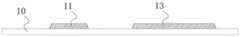
图1是本申请实施例提供的阵列基板的制作方法的流程图;FIG. 1 is a flowchart of a method for fabricating an array substrate provided by an embodiment of the present application;
图2是本申请实施例提供的阵列基板的制作方法的步骤S1的示意图;FIG. 2 is a schematic diagram of step S1 of the method for fabricating an array substrate provided by an embodiment of the present application;
图3是沿图2中A-A线的剖视图;Fig. 3 is a sectional view along line A-A in Fig. 2;
图4是本申请实施例提供的阵列基板的制作方法的步骤S2的示意图;FIG. 4 is a schematic diagram of step S2 of the method for fabricating an array substrate provided by an embodiment of the present application;
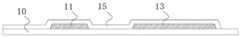
图5是本申请实施例提供的阵列基板的制作方法的步骤S3的示意图;FIG. 5 is a schematic diagram of step S3 of the method for fabricating an array substrate provided by an embodiment of the present application;
图6是沿图5中B-B线的剖视图;Fig. 6 is a sectional view along line B-B in Fig. 5;
图7是本申请实施例提供的阵列基板的制作方法的步骤S4的示意图;7 is a schematic diagram of step S4 of the method for fabricating an array substrate provided by an embodiment of the present application;
图8是沿图7中C-C线的剖视图;Fig. 8 is a sectional view along line C-C in Fig. 7;
图9是本申请实施例提供的阵列基板的制作方法的步骤S5的一个方案示意图;FIG. 9 is a schematic diagram of step S5 of the manufacturing method of the array substrate provided by the embodiment of the present application;
图10本申请实施例提供的阵列基板的制作方法的步骤S5的另一方案示意图;10 is another schematic diagram of step S5 of the manufacturing method of the array substrate provided by the embodiment of the present application;
图11是本申请实施例提供的阵列基板的制作方法的步骤S6的示意图;FIG. 11 is a schematic diagram of step S6 of the method for fabricating an array substrate provided by an embodiment of the present application;
图12是沿图11中D-D线的剖视图;Figure 12 is a sectional view taken along line D-D in Figure 11;
图13是本申请实施例提供的阵列基板的制作方法的步骤S7的示意图;13 is a schematic diagram of step S7 of the method for fabricating an array substrate provided by an embodiment of the present application;
图14至图19是本申请实施例提供的阵列基板的制作方法的步骤S4的分解步骤示意图;FIG. 14 to FIG. 19 are schematic exploded step diagrams of step S4 of the manufacturing method of the array substrate provided by the embodiment of the present application;
图20是本申请实施例提供的阵列基板的制作方法的步骤S3中过蚀刻示意图;FIG. 20 is a schematic diagram of over-etching in step S3 of the manufacturing method of the array substrate provided by the embodiment of the present application;
图21是本申请实施例提供的显示面板的结构示意图。FIG. 21 is a schematic structural diagram of a display panel provided by an embodiment of the present application.
图中标记的含义为:The meanings of the marks in the figure are:
200-显示面板,9-对置基板,8-液晶层;200-display panel, 9-opposing substrate, 8-liquid crystal layer;
100-阵列基板;100-array substrate;
10-衬底基板,101-像素区,102-开口区,103-非开口区,11-栅极,12-栅极线,13-公共电极,14-公共电极线,15-栅极绝缘层,16-附加电极,173-有源层, 171-源极,172-漏极,18-数据线,19-第一钝化层,191-第一过孔,192-第二过孔,193-第三过孔,20-色阻层,21-第二钝化层,221-连接电极,222-本体电极, 223-主干部,224-分支部,23-第三钝化层,24-黑矩阵;10-substrate, 101-pixel area, 102-open area, 103-non-open area, 11-gate, 12-gate line, 13-common electrode, 14-common electrode line, 15-gate insulating layer , 16-Additional electrode, 173-Active layer, 171-Source electrode, 172-Drain electrode, 18-Data line, 19-First passivation layer, 191-First via hole, 192-Second via hole, 193 -Third via hole, 20-Color resist layer, 21-Second passivation layer, 221-Connection electrode, 222-Body electrode, 223-Trunk section, 224-Branch section, 23-Third passivation layer, 24- black matrix;
31-半导体层,311-欧姆接触层,312-沟道层,32-第二金属层,33-第一光阻保护图案,34-第二光阻保护图案,35-源漏金属区,36-有源区。31-semiconductor layer, 311-ohmic contact layer, 312-channel layer, 32-second metal layer, 33-first photoresist protection pattern, 34-second photoresist protection pattern, 35-source-drain metal region, 36- - Active area.
具体实施方式Detailed ways
为了使本申请的目的、技术方案及优点更加清楚明白,以下结合附图及实施例,对本申请进行进一步详细说明。应当理解,此处所描述的具体实施例仅用以解释本申请,并不用于限定本申请。In order to make the purpose, technical solutions and advantages of the present application more clearly understood, the present application will be described in further detail below with reference to the accompanying drawings and embodiments. It should be understood that the specific embodiments described herein are only used to explain the present application, but not to limit the present application.
需说明的是,当部件被称为“固定于”或“设置于”另一个部件,它可以直接或者间接在该另一个部件上。当一个部件被称为是“连接于”另一个部件,它可以是直接或者间接连接至该另一个部件上。术语“上”、“下”、“左”、“右”等指示的方位或位置关系为基于附图所示的方位或位置关系,仅是为了便于描述,而不是指示或暗示所指的装置或元件必须具有特定的方位、以特定的方位构造和操作,因此不能理解为对本专利的限制。术语“第一”、“第二”仅用于便于描述目的,而不能理解为指示或暗示相对重要性或者隐含指明技术特征的数量。“多个”的含义是两个或两个以上,除非另有明确具体的限定。It should be noted that when a component is referred to as being "fixed to" or "disposed on" another component, it can be directly or indirectly on the other component. When an element is referred to as being "connected to" another element, it can be directly or indirectly connected to the other element. The orientation or positional relationship indicated by the terms "upper", "lower", "left", "right", etc. is based on the orientation or positional relationship shown in the drawings, and is only for the convenience of description, rather than indicating or implying the referred device Or elements must have a particular orientation, be constructed and operate in a particular orientation, and therefore should not be construed as a limitation of this patent. The terms "first" and "second" are only used for the purpose of description, and should not be understood as indicating or implying relative importance or implying indicating the number of technical features. "Plurality" means two or more, unless expressly specifically limited otherwise.
为了说明本申请所述的技术方案,以下结合具体附图及实施例进行详细说明。In order to illustrate the technical solutions described in the present application, a detailed description is given below with reference to the specific drawings and embodiments.
请参阅图1,本申请实施例首先提供一种阵列基板的制作方法,包括:Referring to FIG. 1, an embodiment of the present application first provides a method for fabricating an array substrate, including:
步骤S1,如图2和图3所示,在衬底基板10上形成栅极11和公共电极13;Step S1 , as shown in FIG. 2 and FIG. 3 , the
具体地:提供衬底基板10,衬底基板10上设有呈多行多列排布的多个像素区101,每一像素区101包括开口区102和非开口区103。在非开口区103 内形成栅极11和公共电极13。Specifically, a
步骤S2,如图4所示,在栅极11和公共电极13上形成栅极绝缘层15。Step S2 , as shown in FIG. 4 , a
步骤S3,如图5和图6所示,在栅极绝缘层15(图5中省略)上对应非开口区103内形成附加电极16,且,附加电极16在衬底基板10上的投影与公共电极13在衬底基板10上的投影至少部分重叠。Step S3, as shown in FIG. 5 and FIG. 6 , an
步骤S4,如图7和图8所示,在栅极绝缘层15上形成有源层173、源极 171和漏极172。源极171和漏极172分别与有源层173的两端连接。In step S4, as shown in FIGS. 7 and 8, an
由栅极11、有源层173、源极171和漏极172形成薄膜晶体管(TFT)。A thin film transistor (TFT) is formed by the
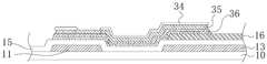
步骤S5,如图9和图10所示,在有源层173、源极171、漏极172和附加电极16上形成第一钝化层19,并在第一钝化层19上对应附加电极16处形成第一过孔191,第一过孔191将部分附加电极16暴露出来,在第一钝化层19 上对应漏极172处形成第二过孔192,第二过孔192将部分漏极172暴露出来。Step S5 , as shown in FIGS. 9 and 10 , a
步骤S6,如图11和图12所示,形成像素电极,具体在第一钝化层19(图 11中省略)上和开口区102内,像素电极包括位于开口区102内的本体电极222 和位于非开口区103内的连接电极221,连接电极221经由第一过孔191与附加电极16电连接,并经由第二过孔192与漏极172电连接。Step S6 , as shown in FIGS. 11 and 12 , a pixel electrode is formed, specifically on the first passivation layer 19 (omitted in FIG. 11 ) and in the
由于像素电极与漏极172电连接,TFT可以驱动像素电极。Since the pixel electrode is electrically connected to the
由于像素电极与附加电极16和漏极172均电连接,因此,附加电极16与漏极172实质电连接。如此,附加电极16与公共电极13之间可以形成存储电容。附加电极16作为存储电容的顶电极,公共电极13作为存储电容的底电极。Since the pixel electrode is electrically connected to both the
本申请实施例提供的阵列基板的制作方法,通过在栅极绝缘层15上形成附加电极16,像素电极经由第一过孔191与附加电极16电连接以及经过第二过孔192与漏极172电连接,因此,附加电极16与像素电极实质电连接,有源层 173不会位于附加电极16和公共电极13之间,有源层173在光线照射下产生的光漏电流不会影响存储电容,保证该存储电容对电荷储存的稳定性,进而能够保证显示画面的稳定性,避免产生画面闪烁等问题;且,附加电极16和公共电极13之间的距离小,有利于提高该存储电容的电容值,提高其电荷储存能力,保证画面显示效果,同时还有利于降低非开口区103的面积,从而提高像素区 101内的开口区102的面积比。In the manufacturing method of the array substrate provided by the embodiment of the present application, by forming the
以下,具体对本申请实施例提供的阵列基板的制作方法的各步骤进行详细描述。Hereinafter, each step of the manufacturing method of the array substrate provided by the embodiments of the present application will be described in detail.
对于步骤S1,请参阅图2和图3,衬底基板10为透明基板,具体为玻璃基板或者塑料基板等。在该步骤S1中,还形成了与栅极11连接的栅极线12,以及与公共电极13连接的公共电极线14。For step S1 , please refer to FIG. 2 and FIG. 3 , the
具体地,该步骤S1是,在衬底基板10上沉积一层金属层(第一金属层),在第一金属层上沉积一层光阻层,提供光罩对该光阻层进行曝光,光阻层部分材料被曝光。对曝光后的光阻层进行显影,光阻层的部分材料被去除,得到与栅极线12、栅极11、公共电极线14和公共电极13对应的保护图案,然后对第一金属层进行湿蚀刻,第一金属层未被保护图案覆盖的部分蚀刻掉,被保护图案覆盖的部分保留,从而得到栅极线12、栅极11、公共电极线14和公共电极13。栅极线12、栅极11、公共电极线14和公共电极13均位于非开口区103 内。Specifically, in this step S1, a metal layer (first metal layer) is deposited on the
第一金属层的材料可以包括铬(Cr)、钼(Mo)、铜(Cu)、钛(Ti)、铝(Al)或氮化钼(MoN)中的至少一种。The material of the first metal layer may include at least one of chromium (Cr), molybdenum (Mo), copper (Cu), titanium (Ti), aluminum (Al), or molybdenum nitride (MoN).
对于步骤S2,如图4所示,通过化学气相沉积法在非开口区103沉积一层绝缘材料,形成能够覆盖上述所说的栅极线12、栅极11、公共电极线14和公共电极13的栅极绝缘层15。栅极绝缘层15的材料可为氧化硅(SiOx)和氮化硅 (SiNx)的至少一种。For step S2, as shown in FIG. 4, a layer of insulating material is deposited on the
对于步骤S3,具体地,在栅极绝缘层15上沉积一层附加导电材料层,在该附加导电材料层上沉积一层光阻层,提供光罩,通过光罩对该光阻层进行曝光,光阻层的部分材料被曝光,对曝光后的光阻层进行显影,得到保护图案,然后对附加导电材料层进行湿蚀刻,附加导电材料层的部分材料被去除,剩余部分即为附加电极16。For step S3, specifically, an additional conductive material layer is deposited on the
对于步骤S4,在栅极绝缘层15上还形成了数据线18,其位于非开口区103,并沿着与栅极线12垂直的方向延伸,同一列像素区101内的源极171连接至同一条数据线18。For step S4, a
附加电极16位于非开口区103内,其与有源层173、源极171和漏极172 之间的相互位置可不做特别限定,但总体上,以参考连接电极221的位置进行设置并有利于上述的第一过孔191的形成为宜。The
请参见附图14至图19,该步骤S4具体是:Please refer to Fig. 14 to Fig. 19, this step S4 is specifically:
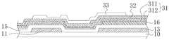
步骤S41,在栅极绝缘层15上形成半导体层31。其中,半导体层31可以包括形成于附加电极16和栅极绝缘层15上的沟道层312(如非晶硅层)和形成于沟道层312上的欧姆接触层311(如掺杂的非晶硅层)。沟道层312和欧姆接触层 311可以分次沉积形成,也可以通过沉积沟道层312并对沟道层312的上部进行离子掺杂得到欧姆接触层311。在半导体层31上沉积一金属层(第二金属层 32),在第二金属层32上沉积光阻层。提供一灰阶光罩(或半色调光罩),该灰阶光罩(或半色调光罩)上设有透光区、非透光区以及半透光区,用于在光阻层上分别形成全曝光区、未曝光区和半曝光区。使用该灰阶光罩(或半色调光罩)对光阻层进行曝光,经显影后,得到第一光阻保护图案33,如图14所示,第一光阻保护图案33呈凸-凹-凸状,其两端的高度大于中部的高度。In step S41 , the
步骤S42,如图15所示,对第二金属层32进行湿蚀刻,第二金属层32上未被第一光阻保护图案33覆盖的区域被去除,得到源漏金属区35。Step S42 , as shown in FIG. 15 , wet etching is performed on the
步骤S43,如图16所示,对半导体层31进行干蚀刻,半导体层31上未被第一光阻保护图案33和源漏金属区35覆盖的区域被去除,得到有源区36。In step S43 , as shown in FIG. 16 , dry etching is performed on the
步骤S44,如图17所示,对第一光阻保护图案33进行灰化,第一光阻保护图案33的高度整体降低,第一光阻保护图案33的高度较低的中部被完全去除,得到第二光阻保护图案34,第二光阻保护图案34包括两个相间隔的保护部,分别覆盖源漏金属区35的两端。In step S44, as shown in FIG. 17, the first
步骤S45,如图18所示,对源漏金属区35进行湿蚀刻,得到源极171和漏极172。Step S45 , as shown in FIG. 18 , wet etching is performed on the source-
如此,源极171在衬底基板10上的投影位于有源区36在衬底基板10上的投影内;漏极172在衬底基板10上的投影位于有源层173在衬底基板10上的投影内。In this way, the projection of the
步骤S46,如图19所示,以第二光阻保护图案34为保护图案,对有源区 36进行干蚀刻,欧姆接触层311的位于源极171和漏极172之间的部分被蚀刻去除,沟道层312的中部保留,如此,得到下层为沟道层312、上层为欧姆接触层311的有源层173。Step S46 , as shown in FIG. 19 , dry etching is performed on the
第二金属层32的材料可以包括Cr、Mo、Cu、Ti、Al或MoN中的至少一种。例如,在本实施例中,第二金属层32为Mo/Al/Mo层、MoN/Al/Mo或 Mo/Al/MoN层,Al具有良好的导电性和低成本优点,而Mo材料能够有效防止 Al原子向非晶硅层的扩散,防止有源层173产生光漏电流,改善TFT的电学特性。可以理解,此处仅作示例,第二金属层的材料构成并不以此为限。The material of the
对于步骤S5,如图9所示,在源极171、漏极172、数据线18和栅极绝缘层15上沉积一绝缘材料层,且在该绝缘层上沉积光阻层,提供光罩,使用光罩对光阻层进行曝光,显影后,光阻层上对应附加电极16位置处和漏极172的位置处被去除,对该绝缘材料层进行干蚀刻,对应附加电极16位置处和漏极172 的位置处的绝缘材料被去除,如此,形成了位于非开口区103的第一钝化层19,且第一钝化层19上对应附加电极16处形成第一过孔191,对应漏极172处形成第二过孔192,第一过孔191将附加电极16部分暴露出来,第二过孔192将漏极172部分暴露出来。For step S5, as shown in FIG. 9, an insulating material layer is deposited on the
步骤S5中所说的绝缘材料可以包括无机绝缘材料,诸如氧化硅、氮化硅、氮氧化硅、氧化铝、氧化钛或氧化锌等。然而,此处仅作示例,具体不限于此。The insulating material in step S5 may include inorganic insulating materials, such as silicon oxide, silicon nitride, silicon oxynitride, aluminum oxide, titanium oxide, or zinc oxide. However, this is only an example, and is not specifically limited to this.
步骤S6,如图11和图12所示,在第一钝化层19上和开口区102内沉积一层透明导电材料层,在该透明导电材料层上沉积光阻层,提供光罩(像素电极光罩),使用该像素电极光罩对光阻层进行曝光,显影后,光阻层形成与所要得到的像素电极相对应的保护图案,使用该保护图案对透明导电材料层进行湿蚀刻,得到像素电极。Step S6, as shown in FIG. 11 and FIG. 12 , deposit a layer of transparent conductive material on the
透明导电材料层可为ITO(Indium Tin Oxide,氧化铟锡)层。当然,此处仅为示例,在其他可选实施例中,透明导电材料层还可以为AZO(Aluminum Zinc Oxide,氧化铝锌)等。The transparent conductive material layer may be an ITO (Indium Tin Oxide, indium tin oxide) layer. Of course, this is only an example, and in other optional embodiments, the transparent conductive material layer may also be AZO (Aluminum Zinc Oxide, aluminum oxide zinc) or the like.
其中,如图11所示,本体电极222包括主干部223以及连接于主干部223 的多个分支部224。在本实施例中,主干部223呈十字状,本体电极222被划分为多个部分(多个畴,本实施例中为四个畴),不同畴内的分支部224的延伸方向不同,同一畴内的多个分支部224相互平行且间隔。如此,使用该像素电极对液晶分子进行偏转控制时,对应不同畴的液晶分子的偏转方向有差别,能够解决显示色偏问题。Wherein, as shown in FIG. 11 , the
主干部223的特征尺寸(线宽)、分支部224的特征尺寸均小于连接电极221 的特征尺寸。The feature size (line width) of the
例如,连接电极221的特征尺寸在20微米以上,其尺寸具体如20微米× 30微米。主干部223的线宽为2微米~8微米,分支部224的线宽为2微米~8 微米。当然,此处仅作示例以用于说明,并不以此为限,在其他可选实施例中,连接电极221、主干部223以及分支部224的特征尺寸均可以有其他数值。For example, the feature size of the
因此,在本实施例中,上述步骤S3所使用的光罩与该步骤S6中为形成像素电极而使用的像素电极光罩。如此,形成该附加电极16不需要额外的光罩,因此,该阵列基板的制作方法中光罩成本不会增加。并且,这使得附加电极16 的位置与连接电极221的位置相对应,更有利于二者之间通过第一过孔191进行连接。Therefore, in this embodiment, the photomask used in the above step S3 and the pixel electrode photomask used in the step S6 for forming the pixel electrodes. In this way, an additional photomask is not required to form the
基于此,再次对步骤S3进行说明。Based on this, step S3 will be described again.
具体地,在一个实现方案中,使用像素电极光罩而形成附加电极16的步骤是:Specifically, in one implementation, the steps of using the pixel electrode mask to form the
提供像素电极光罩,对位于附加导电材料层上方的光阻层进行曝光,对曝光后的光阻层进行显影,得到与像素电极的图案相对应的保护图案,对该附加导电材料层进行湿蚀刻,首先,蚀刻掉该附加导电材料层上未被保护图案覆盖的部分,然后蚀刻掉与本体电极222的图案相对应的部分,剩余的部分即为与连接电极221的图案相对应的附加电极16,如图20所示。A pixel electrode mask is provided, the photoresist layer above the additional conductive material layer is exposed, and the exposed photoresist layer is developed to obtain a protection pattern corresponding to the pattern of the pixel electrode, and the additional conductive material layer is wetted Etching, first, the part of the additional conductive material layer that is not covered by the protective pattern is etched away, and then the part corresponding to the pattern of the
在这里,湿蚀刻为一过蚀刻步骤:由于湿蚀刻过程中所使用的蚀刻液的各向同性,蚀刻液在对该附加导电材料层进行纵向蚀刻的同时,还发生侧向蚀刻,随着侧向蚀刻的增加,在被蚀刻的材料层上获得较细且较薄的图案,而不受限于曝光时的光罩的特征尺寸。Here, the wet etching is an over-etching step: due to the isotropy of the etching solution used in the wet etching process, while the etching solution performs longitudinal etching on the additional conductive material layer, lateral etching also occurs. Increasing to etch, finer and thinner patterns are obtained on the layer of material being etched, independent of the feature size of the reticle at the time of exposure.
具体地,通过提高该步骤S3中湿蚀刻所使用的蚀刻液中酸的浓度和/或增加湿蚀刻的作用时间,能够使得附加该附加导电材料层中对应本体电极222的图案的部分在侧向上完全被蚀刻去除。从而,剩余的部分即为附加电极16。Specifically, by increasing the concentration of the acid in the etching solution used in the wet etching in step S3 and/or increasing the action time of the wet etching, the portion corresponding to the pattern of the
在该实现方案中,步骤S3中湿蚀刻的时间大于步骤S6中湿蚀刻的时间;或,步骤S3中湿蚀刻所使用的蚀刻液的浓度大于步骤S6中所使用的蚀刻液的浓度;或者,步骤S3中湿蚀刻的时间大于步骤S6中湿蚀刻的时间,并且步骤S3中湿蚀刻所使用的蚀刻液的浓度大于步骤S6中所使用的蚀刻液的浓度。In this implementation scheme, the time of wet etching in step S3 is greater than the time of wet etching in step S6; or, the concentration of the etching solution used in the wet etching in step S3 is greater than the concentration of the etching solution used in step S6; or, The time of wet etching in step S3 is greater than the time of wet etching in step S6, and the concentration of the etching solution used in the wet etching in step S3 is greater than that of the etching solution used in step S6.
或者,在另一个实现方案中,使用像素电极光罩而形成附加电极16的步骤是:Alternatively, in another implementation, the steps of using the pixel electrode mask to form the
提供像素电极光罩,对位于附加导电材料层上方的光阻层进行曝光,对曝光后的光阻层进行显影,得到与连接电极221的图案相对应的保护图案,对该附加导电材料层进行湿蚀刻,得到与连接电极221的图案相对应的附加电极16。A pixel electrode mask is provided, the photoresist layer above the additional conductive material layer is exposed, and the exposed photoresist layer is developed to obtain a protection pattern corresponding to the pattern of the
在这里,对光阻层的曝光为一强曝光过程:光阻层中的光敏分子在光线(紫外光)的照射下并吸收光线能量后能够发生部分基团的脱离,导致光阻层材料发生变性。在照射的过程中,光线不可避免地发生散射现象,并且光线在光阻层的表面还会发生反射,最终导致光线能够照射到的区域大于光罩的透光区域,导致光阻层显影后得到的保护图案的特征尺寸小于光罩的特征尺寸。Here, the exposure of the photoresist layer is a strong exposure process: the photosensitive molecules in the photoresist layer can be detached from some groups under the irradiation of light (ultraviolet light) and absorb the light energy, resulting in the occurrence of photoresist layer materials. transsexual. In the process of irradiation, the light is inevitably scattered, and the light will be reflected on the surface of the photoresist layer, and finally the area that the light can irradiate is larger than the light-transmitting area of the photomask, resulting in the photoresist layer after development. The feature size of the protection pattern is smaller than the feature size of the reticle.
具体地,通过提高曝光的光照时间和/或光照强度,位于附加导电材料层上方的光阻层上对应主干部223和分支部224的图案的部分也能够被完全曝光,从而在显影后被去除,显影后的光阻层仅保留对应连接电极221的图案的部分。结果是,在进行后续湿蚀刻时未被覆盖的部分可以蚀刻去除,剩余的部分即为附加电极16。Specifically, by increasing the light exposure time and/or light intensity, the portion of the photoresist layer located above the additional conductive material layer corresponding to the pattern of the
在该实现方案中,步骤S3中曝光的时间大于步骤S6中曝光的时间;或,步骤S3中曝光时的光照强度大于步骤S6中曝光的曝光强度;或者,步骤S3 中曝光的时间大于步骤S6中曝光的时间,且步骤S3中曝光时的光照强度大于步骤S6中曝光的曝光强度。In this implementation scheme, the exposure time in step S3 is greater than the exposure time in step S6; or, the light intensity during exposure in step S3 is greater than the exposure intensity in step S6; or, the exposure time in step S3 is greater than that in step S6 and the light intensity during exposure in step S3 is greater than the exposure intensity of exposure in step S6.
可选地,在本实施例中,附加电极16的材料与像素电极的材料相同,以有利于根据步骤S6的蚀刻工艺和/或曝光工艺来实施步骤S3。Optionally, in this embodiment, the material of the
当然,在其他可选实施例中,在步骤S3中,附加导电材料层可以如同栅极 11或源极171等为非透明导电材料层,如Cr、Mo、Cu、Ti、Al或MoN中的至少一种。在此基础上,通过调整强曝光的光照强度和/或光照时间、湿蚀刻的蚀刻液浓度和/或湿蚀刻时间来得到所需要的连接电极221,对此不在赘述。Of course, in other optional embodiments, in step S3, the additional conductive material layer may be a non-transparent conductive material layer such as the
基于上述的过蚀刻或强曝光步骤,附加电极16的特征尺寸小于连接电极 221的特征尺寸,也即,在该步骤S3中,附加电极16在衬底基板10上的投影位于连接电极221在衬底基板10上的投影的内部。Based on the above-mentioned over-etching or strong exposure step, the feature size of the
进一步地,结合上述连接电极221的制作步骤,在本实施例中,附加电极 16在衬底基板10上的投影与有源层173在衬底基板10上的投影部分重合。也即,步骤S3中,有源层173形成在栅极绝缘层15和附加电极16上,如图8 所示。这样的好处是,在非开口区102的有限面积内,可以同时保证附加电极 16和有源层173各自有足够的面积。当然,在其他可选实施例中,在非开口区 102的面积足够的情况下,有源层173可以不形成在附加电极16上而是与附加电极16同层设置。Further, in combination with the above-mentioned fabrication steps of the connecting
进一步地,结合上述有源层173、源极171和漏极172的制作步骤,在本实施例中,附加电极16在衬底基板10上的投影与漏极172在衬底基板10上的投影部分重合,如图8和图9所示。这样的结果是,第二过孔192可以形成在漏极172的边缘处直至与第一过孔191相连通成为一个大的第三过孔193,该第三过孔193同时暴露出部分附加电极16和部分漏极172。如此,第三过孔193 的尺寸可以增大,第三过孔193的制作精度要求可以降低,制作难度可以降低。Further, in combination with the above-mentioned fabrication steps of the
当然,在其他实施例中,根据漏极172和附加电极16的位置,或者是第一过孔191和第二过孔192的其他功能,又或者是在制作成本允许的情况下,第一过孔191和第二过孔192可以相间隔设置,如图10所示。Of course, in other embodiments, according to the positions of the
在其他可选实施例中,在允许的情况下,步骤S3中可采用额外一光罩来形成附加电极16。具体步骤可以如,在栅极绝缘层15上对应非开口区103内沉积附加导电材料层,并在附加导电材料层上沉积光阻层;使用光罩对该光阻层进行曝光,对曝光后的光阻层显影,得到保护图案;对附加导电材料层进行湿蚀刻(非过蚀刻),得到与保护图案一致的附加电极16。In other optional embodiments, if permitted, an additional photomask may be used to form the
在一个实施例中,请结合参阅图9和图10,本申请实施例提供的阵列基板的制作方法在步骤S5之后、步骤S6之前还包括:在第一钝化层19上和开口区102内形成色阻层20,在色阻层20上对应非开口区103形成第二钝化层21,像素电极形成于第二钝化层21上,且,第一过孔191和第二过孔192同时贯穿色阻层20和第二钝化层21。如此,所得到的基板为COA(Color on Array,色阻层20位于阵列基板100上)型阵列基板100。In one embodiment, please refer to FIG. 9 and FIG. 10 in conjunction with FIG. 9 and FIG. 10 , after step S5 and before step S6 , the method for fabricating the array substrate provided by the embodiment of the present application further includes: on the
第二钝化层21的材料可以包括无机绝缘材料,诸如氧化硅、氮化硅、氮氧化硅、氧化铝、氧化钛或氧化锌等。The material of the
此外,请参阅图1和图13,在一个实施例中,该阵列基板的制作方法还包括步骤S7,在像素电极和第二钝化层21上对应非开口区103形成第三钝化层 23,并在第三钝化层23上对应非开口区103形成黑矩阵24等。如此,得到阵列基板100。In addition, please refer to FIG. 1 and FIG. 13 , in one embodiment, the manufacturing method of the array substrate further includes step S7 , forming a
请结合参阅图11和图13,本申请实施例还提供一种阵列基板100,其通过上述各实施例所说的阵列基板的制作方法所制作得到。具体地,该阵列基板100 包括:Please refer to FIG. 11 and FIG. 13 in conjunction with FIG. 11 , an embodiment of the present application further provides an
衬底基板10,衬底基板10上设有多个呈阵列排布的像素区101,每一像素区101包括开口区102和非开口区103,非开口区103内设有栅极11、栅极线 12、公共电极13和公共电极线14;The
栅极绝缘层15,设于栅极11、栅极线12、公共电极13、公共电极线14 以及衬底基板10上;The
附加电极16,设于栅极绝缘层15上,且附加电极16在衬底基板10上的投影与公共电极13在衬底基板10上的投影至少部分重叠;The
有源层173,设于栅极绝缘层15上;The
源极171,设于有源层173上;The
漏极172,设于有源层173上且与源极171相间隔;由栅极11、有源层173、源极171和漏极172形成TFT;The
第一钝化层19,设于有源层173、源极171、漏极172和附加电极16上,且第一钝化层19对应附加电极16处设有第一过孔191,对应漏极172处设有第二过孔192;The
像素电极,包括位于开口区102内的本体电极222以及设于第一钝化层19 上且位于非开口区103内的连接电极221,连接电极221经由第一过孔191与附加电极16电连接,并经由第二过孔192与漏极172电连接。The pixel electrode includes a
由于像素电极与漏极172电连接,TFT可以驱动像素电极。Since the pixel electrode is electrically connected to the
由于像素电极与附加电极16和漏极172均电连接,因此,附加电极16与漏极172实质电连接。如此,附加电极16与公共电极13之间因栅极绝缘层15 而绝缘,二者之间可以形成存储电容。附加电极16作为存储电容的顶电极,公共电极13作为存储电容的底电极。Since the pixel electrode is electrically connected to both the
本申请实施例提供的阵列基板100,其栅极绝缘层15上设有附加电极16,像素电极经由第一过孔191与附加电极16电连接以及经过第二过孔192与漏极172电连接,附加电极16与像素电极实质电连接,在附加电极16和公共电极 13之间形成存储电容时,有源层173不会位于附加电极16和公共电极13之间,有源层173在光线照射下产生的光漏电流不会影响存储电容,保证该存储电容对电荷储存的稳定性,进而能够保证显示画面的稳定性,避免产生画面闪烁等问题;且,附加电极16和公共电极13之间的距离小,有利于提高该存储电容的电容值,提高其电荷储存能力,保证画面显示效果,同时还有利于降低非开口区103的面积,从而提高像素区101内开口区102的面积比。In the
如图13所示,附加电极16在衬底基板10上的投影与有源层173在衬底基板10上的投影部分重合,也即,有源层173位于栅极绝缘层15和附加电极16 上,这样可以在非开口区102的有限面积内同时保证附加电极16和有源层173 各自有足够的面积。当然,在其他可选实施例中,在非开口区102的面积足够的情况下,有源层173可以不形成在附加电极16上而是与附加电极16同层设置。As shown in FIG. 13 , the projection of the
进一步地,请继续参阅图13,在本实施例中,附加电极16在衬底基板10 上的投影与漏极172在衬底基板10上的投影部分重合。这样的结果是,第二过孔192可以形成在漏极172的边缘处直至与第一过孔191相连通成为一个大的第三过孔193,该第三过孔193同时暴露出部分附加电极16和部分漏极172。如此,第三过孔193的尺寸可以增大,第三过孔193的制作精度要求可以降低,制作难度可以降低。Further, please continue to refer to FIG. 13 , in this embodiment, the projection of the
当然,在其他可选实施例中,根据漏极172和附加电极16的位置,或者是第一过孔191和第二过孔192的其他功能,又或者是在制作成本允许的情况下,第一过孔191和第二过孔192可以相间隔设置,请参考前述的图10。Of course, in other optional embodiments, according to the positions of the
栅极11、栅极线12、公共电极13和公共电极线14的材料可以包括Cr、 Mo、Cu、Ti、Al或MoN中的至少一种。栅极绝缘层15的材料可包括氧化硅 (SiOx)和氮化硅(SiNx)的至少一种。有源层173可以包括下层的非晶硅层和上层的欧姆接触层。源极171和漏极172的材料可以包括Cr、Mo、Cu、Ti、Al或MoN中的至少一种。第一绝缘层的材料可以包括无机绝缘材料,诸如氧化硅、氮化硅、氮氧化硅、氧化铝、氧化钛或氧化锌等。Materials of the
像素电极的材料为ITO,或者是AZO等。The material of the pixel electrode is ITO, or AZO or the like.
附加电极16的材料可包括非透明导电材料,如Cr、Mo、Cu、Ti、Al或 MoN中的至少一种;或者,附加电极16的材料包括透明导电材料,如ITO或者是AZO等。在本实施例中,附加电极16的材料与像素电极的材料相同。The material of the
如图11和图13所示,附加电极16的特征尺寸小于连接电极221的特征尺寸,也即,附加电极16在衬底基板10上的投影位于连接电极221在衬底基板 10上的投影的内部。As shown in FIG. 11 and FIG. 13 , the feature size of the
如图13所示,源极171在衬底基板10上的投影位于有源层173在衬底基板10上的投影的内部;漏极172在衬底基板10上的投影位于有源层173在衬底基板10上的投影的内部。As shown in FIG. 13 , the projection of the
请继续参阅图11和图13,在一个实施例中,该阵列基板100还包括色阻层20和第二钝化层21,色阻层20设于第一钝化层19上及开口区102内,第二钝化层21设于色阻层20上且对应非开口区103,第一过孔191和第二过孔 192同时贯穿色阻层20和第二钝化层21;像素电极形成于第二钝化层21上及开口区102内。Please continue to refer to FIG. 11 and FIG. 13 , in one embodiment, the
第二绝缘层的材料可以包括无机绝缘材料,诸如氧化硅、氮化硅、氮氧化硅、氧化铝、氧化钛或氧化锌等。The material of the second insulating layer may include inorganic insulating materials such as silicon oxide, silicon nitride, silicon oxynitride, aluminum oxide, titanium oxide, or zinc oxide, and the like.
在一个实施例中,如图13所示,该阵列基板100还包括形成在像素电极和第二钝化层21上对应非开口区103的第三钝化层23,以及形成在第三钝化层 23上对应非开口区103的黑矩阵24。In one embodiment, as shown in FIG. 13 , the
请参阅图21,本申请实施例还提供一种显示面板200,包括上述各实施例所说的阵列基板100、与阵列基板100相对设置的对置基板9,以及夹设于阵列基板100和对置基板9之间的液晶层8。Referring to FIG. 21 , an embodiment of the present application further provides a
本申请实施例提供的显示面板200,其阵列基板100中的存储电容不会受到有源层173在光线照射下产生的光漏电流的影响,存储电容的电荷储存稳定,能够保证显示画面的稳定性,避免产生画面闪烁等问题;且,附加电极16和公共电极13之间的距离小,该存储电容具有高的电容值,高的电荷储存能力,保证画面显示效果,同时非开口区103的面积可以降低,从而像素区101内开口区102的面积比可以提高。In the
以上所述仅为本申请的较佳实施例而已,并不用以限制本申请,凡在本申请的精神和原则之内所作的任何修改、等同替换和改进等,均应包含在本申请的保护范围之内。The above descriptions are only preferred embodiments of the present application, and are not intended to limit the present application. Any modifications, equivalent replacements and improvements made within the spirit and principles of the present application shall be included in the protection of the present application. within the range.
Claims (9)
Translated fromChinesePriority Applications (1)
| Application Number | Priority Date | Filing Date | Title |
|---|---|---|---|
| CN202110662463.4ACN113394166B (en) | 2021-06-15 | 2021-06-15 | Manufacturing method of array substrate, array substrate and display panel |
Applications Claiming Priority (1)
| Application Number | Priority Date | Filing Date | Title |
|---|---|---|---|
| CN202110662463.4ACN113394166B (en) | 2021-06-15 | 2021-06-15 | Manufacturing method of array substrate, array substrate and display panel |
Publications (2)
| Publication Number | Publication Date |
|---|---|
| CN113394166A CN113394166A (en) | 2021-09-14 |
| CN113394166Btrue CN113394166B (en) | 2022-02-08 |
Family
ID=77621181
Family Applications (1)
| Application Number | Title | Priority Date | Filing Date |
|---|---|---|---|
| CN202110662463.4AActiveCN113394166B (en) | 2021-06-15 | 2021-06-15 | Manufacturing method of array substrate, array substrate and display panel |
Country Status (1)
| Country | Link |
|---|---|
| CN (1) | CN113394166B (en) |
Families Citing this family (6)
| Publication number | Priority date | Publication date | Assignee | Title |
|---|---|---|---|---|
| CN114355684A (en)* | 2021-12-24 | 2022-04-15 | 滁州惠科光电科技有限公司 | Array substrate, manufacturing method and display panel |
| US12176355B2 (en) | 2022-05-11 | 2024-12-24 | Tcl China Star Optoelectronics Technology Co., Ltd. | Display panel and manufacturing method thereof |
| CN114967257B (en)* | 2022-05-11 | 2023-10-03 | Tcl华星光电技术有限公司 | Display panel and manufacturing method thereof |
| CN115390302A (en)* | 2022-08-23 | 2022-11-25 | 广州华星光电半导体显示技术有限公司 | Liquid crystal display panel and manufacturing method thereof |
| EP4597485A1 (en)* | 2022-09-28 | 2025-08-06 | Boe Technology Group Co., Ltd. | Display substrate and preparation method therefor, and display apparatus |
| CN115981059B (en)* | 2023-03-20 | 2023-06-23 | 惠科股份有限公司 | Liquid crystal display panel and liquid crystal display |
Citations (4)
| Publication number | Priority date | Publication date | Assignee | Title |
|---|---|---|---|---|
| US6411346B1 (en)* | 1998-06-16 | 2002-06-25 | Mitsubishi Denki Kabushiki Kaisha | Active matrix LCD in which a change in the storage capacitance Cs due to having multiple exposure regions is compensated for by a change in the coupling capacitance Cgd |
| CN105470269A (en)* | 2016-01-26 | 2016-04-06 | 深圳市华星光电技术有限公司 | TFT array substrate and manufacturing method thereof |
| CN105572995A (en)* | 2016-02-01 | 2016-05-11 | 昆山龙腾光电有限公司 | Array substrate and manufacturing method thereof and liquid crystal display device |
| CN110426904A (en)* | 2019-06-27 | 2019-11-08 | 惠科股份有限公司 | Array substrate and display device |
Family Cites Families (2)
| Publication number | Priority date | Publication date | Assignee | Title |
|---|---|---|---|---|
| KR100433209B1 (en)* | 2001-06-25 | 2004-05-27 | 엘지.필립스 엘시디 주식회사 | Array Substrate of Liquid Crystal Display Device and Fabricating Method Thereof |
| CN109116647B (en)* | 2018-09-17 | 2021-08-27 | 京东方科技集团股份有限公司 | Array substrate, preparation method thereof and display device |
- 2021
- 2021-06-15CNCN202110662463.4Apatent/CN113394166B/enactiveActive
Patent Citations (4)
| Publication number | Priority date | Publication date | Assignee | Title |
|---|---|---|---|---|
| US6411346B1 (en)* | 1998-06-16 | 2002-06-25 | Mitsubishi Denki Kabushiki Kaisha | Active matrix LCD in which a change in the storage capacitance Cs due to having multiple exposure regions is compensated for by a change in the coupling capacitance Cgd |
| CN105470269A (en)* | 2016-01-26 | 2016-04-06 | 深圳市华星光电技术有限公司 | TFT array substrate and manufacturing method thereof |
| CN105572995A (en)* | 2016-02-01 | 2016-05-11 | 昆山龙腾光电有限公司 | Array substrate and manufacturing method thereof and liquid crystal display device |
| CN110426904A (en)* | 2019-06-27 | 2019-11-08 | 惠科股份有限公司 | Array substrate and display device |
Also Published As
| Publication number | Publication date |
|---|---|
| CN113394166A (en) | 2021-09-14 |
Similar Documents
| Publication | Publication Date | Title |
|---|---|---|
| CN113394166B (en) | Manufacturing method of array substrate, array substrate and display panel | |
| CN100504524C (en) | Array substrate of liquid crystal display device and manufacturing method thereof | |
| CN100451781C (en) | Liquid crystal display device including polycrystalline silicon thin film transistor and method of fabricating the same | |
| JP4607418B2 (en) | Array substrate for liquid crystal display device and manufacturing method thereof | |
| CN1637530B (en) | Manufacturing method of transflective liquid crystal display device | |
| US7785940B2 (en) | TFT array substrate and method for fabricating the same | |
| US8362526B2 (en) | Liquid crystal display device and fabricating method thereof | |
| US8730418B2 (en) | Array substrate and method for manufacturing the same | |
| CN101995713B (en) | TFT-LCD array substrate and manufacturing method thereof | |
| US5981972A (en) | Actived matrix substrate having a transistor with multi-layered ohmic contact | |
| CN105304643A (en) | TFT array substrate and preparation method thereof | |
| CN101825814A (en) | TFT (Thin Film Transistor)-LCD (Liquid Crystal Display) array baseplate and manufacturing method thereof | |
| CN210325749U (en) | Array substrate and display panel | |
| WO2017124673A1 (en) | Method for manufacturing array substrate and liquid crystal display panel | |
| CN101320740A (en) | Display substrate, display substrate manufacturing method, and display device having display substrate | |
| US20100320470A1 (en) | Thin film transistor array panel and method for manufacturing the same | |
| WO2014153958A1 (en) | Array substrate, method for manufacturing array substrate and display device | |
| US20120113377A1 (en) | Array substrate and manufacturing method thereof, and liquid crystal display | |
| US7214965B2 (en) | Thin film transistor array panel and method of manufacturing the same | |
| CN101799603B (en) | TFT-LCD array substrate and manufacture method thereof | |
| US20160300867A1 (en) | Array substrate and liquid crystal display module including tft having improved mobility and method of fabricating the same | |
| US20030123009A1 (en) | Array substrate for IPS mode liquid crystal display device and fabricating method for the same | |
| CN109300841B (en) | The manufacturing method of array substrate | |
| JP4392843B2 (en) | Thin film transistor array substrate, manufacturing method thereof, and liquid crystal display panel | |
| KR20070115370A (en) | Display device with improved aperture ratio and manufacturing method thereof |
Legal Events
| Date | Code | Title | Description |
|---|---|---|---|
| PB01 | Publication | ||
| PB01 | Publication | ||
| SE01 | Entry into force of request for substantive examination | ||
| SE01 | Entry into force of request for substantive examination | ||
| GR01 | Patent grant | ||
| GR01 | Patent grant |