CN113391471B - Spatial light modulator and its preparation method - Google Patents
Spatial light modulator and its preparation methodDownload PDFInfo
- Publication number
- CN113391471B CN113391471BCN202110658175.1ACN202110658175ACN113391471BCN 113391471 BCN113391471 BCN 113391471BCN 202110658175 ACN202110658175 ACN 202110658175ACN 113391471 BCN113391471 BCN 113391471B
- Authority
- CN
- China
- Prior art keywords
- modulation layer
- unit
- spatial light
- light modulator
- modulation
- Prior art date
- Legal status (The legal status is an assumption and is not a legal conclusion. Google has not performed a legal analysis and makes no representation as to the accuracy of the status listed.)
- Active
Links
Images


Classifications
- G—PHYSICS
- G02—OPTICS
- G02F—OPTICAL DEVICES OR ARRANGEMENTS FOR THE CONTROL OF LIGHT BY MODIFICATION OF THE OPTICAL PROPERTIES OF THE MEDIA OF THE ELEMENTS INVOLVED THEREIN; NON-LINEAR OPTICS; FREQUENCY-CHANGING OF LIGHT; OPTICAL LOGIC ELEMENTS; OPTICAL ANALOGUE/DIGITAL CONVERTERS
- G02F1/00—Devices or arrangements for the control of the intensity, colour, phase, polarisation or direction of light arriving from an independent light source, e.g. switching, gating or modulating; Non-linear optics
- G02F1/01—Devices or arrangements for the control of the intensity, colour, phase, polarisation or direction of light arriving from an independent light source, e.g. switching, gating or modulating; Non-linear optics for the control of the intensity, phase, polarisation or colour
- G02F1/03—Devices or arrangements for the control of the intensity, colour, phase, polarisation or direction of light arriving from an independent light source, e.g. switching, gating or modulating; Non-linear optics for the control of the intensity, phase, polarisation or colour based on ceramics or electro-optical crystals, e.g. exhibiting Pockels effect or Kerr effect
- G02F1/0305—Constructional arrangements
- G02F1/0316—Electrodes
- G—PHYSICS
- G02—OPTICS
- G02F—OPTICAL DEVICES OR ARRANGEMENTS FOR THE CONTROL OF LIGHT BY MODIFICATION OF THE OPTICAL PROPERTIES OF THE MEDIA OF THE ELEMENTS INVOLVED THEREIN; NON-LINEAR OPTICS; FREQUENCY-CHANGING OF LIGHT; OPTICAL LOGIC ELEMENTS; OPTICAL ANALOGUE/DIGITAL CONVERTERS
- G02F1/00—Devices or arrangements for the control of the intensity, colour, phase, polarisation or direction of light arriving from an independent light source, e.g. switching, gating or modulating; Non-linear optics
- G02F1/01—Devices or arrangements for the control of the intensity, colour, phase, polarisation or direction of light arriving from an independent light source, e.g. switching, gating or modulating; Non-linear optics for the control of the intensity, phase, polarisation or colour
- G02F1/09—Devices or arrangements for the control of the intensity, colour, phase, polarisation or direction of light arriving from an independent light source, e.g. switching, gating or modulating; Non-linear optics for the control of the intensity, phase, polarisation or colour based on magneto-optical elements, e.g. exhibiting Faraday effect
- G—PHYSICS
- G02—OPTICS
- G02F—OPTICAL DEVICES OR ARRANGEMENTS FOR THE CONTROL OF LIGHT BY MODIFICATION OF THE OPTICAL PROPERTIES OF THE MEDIA OF THE ELEMENTS INVOLVED THEREIN; NON-LINEAR OPTICS; FREQUENCY-CHANGING OF LIGHT; OPTICAL LOGIC ELEMENTS; OPTICAL ANALOGUE/DIGITAL CONVERTERS
- G02F1/00—Devices or arrangements for the control of the intensity, colour, phase, polarisation or direction of light arriving from an independent light source, e.g. switching, gating or modulating; Non-linear optics
- G02F1/01—Devices or arrangements for the control of the intensity, colour, phase, polarisation or direction of light arriving from an independent light source, e.g. switching, gating or modulating; Non-linear optics for the control of the intensity, phase, polarisation or colour
- G02F1/11—Devices or arrangements for the control of the intensity, colour, phase, polarisation or direction of light arriving from an independent light source, e.g. switching, gating or modulating; Non-linear optics for the control of the intensity, phase, polarisation or colour based on acousto-optical elements, e.g. using variable diffraction by sound or like mechanical waves
Landscapes
- Physics & Mathematics (AREA)
- Nonlinear Science (AREA)
- General Physics & Mathematics (AREA)
- Optics & Photonics (AREA)
- Engineering & Computer Science (AREA)
- Chemical & Material Sciences (AREA)
- Ceramic Engineering (AREA)
- Crystallography & Structural Chemistry (AREA)
- Power Engineering (AREA)
- Optical Modulation, Optical Deflection, Nonlinear Optics, Optical Demodulation, Optical Logic Elements (AREA)
Abstract
Translated fromChinese
Description
Translated fromChinese技术领域technical field
本公开涉及光学技术领域,尤其涉及一种空间光调制器及其制备方法。The present disclosure relates to the field of optical technology, in particular to a spatial light modulator and a preparation method thereof.
背景技术Background technique
空间光调制器是一种能够调节光波的波长、振幅和相位等光学参量的光学器件。空间光调制器在空间光通信、生化传感器、光学计算机和数字全息成像等领域具有重要作用。随着信息时代的快速发展,空间光调制器有望促进光学宽带网络等产品的性能提升。A spatial light modulator is an optical device that can adjust optical parameters such as wavelength, amplitude, and phase of light waves. Spatial light modulators play an important role in the fields of spatial optical communication, biochemical sensors, optical computers, and digital holographic imaging. With the rapid development of the information age, spatial light modulators are expected to facilitate the performance improvement of products such as optical broadband networks.
传统的空间光调制器包含稳定性较低的有机材料和复杂的结构。由于材料和结构的性能限制,空间光调制器存在插入损耗高和调制速度低的缺点。目前空间光调制器的种类主要是液晶空间光调制器。液晶空间光调制器的主要功能材料是液晶,还包括导向层和封框胶。封框胶等连接结构容易移动,存在固定稳定性弱的问题。液晶的使用温度通常不超过50℃。液晶、导向层和封框胶都是温度稳定性较低的有机物,在光照和较高温度下使用容易老化,存在使用温度低、使用寿命短的问题。液晶空间光调制器的调制机理通常采用液晶的电致双折射效应,由于液晶材料、液晶层的厚度的最小均匀性和液晶层最小厚度的限制,液晶空间光调制器存在插入损耗高和调制速度低的缺点,插入损耗为1.5dB(反射率72%),调制速度通常在百赫兹量级。Conventional spatial light modulators contain less stable organic materials and complex structures. Due to the performance limitations of materials and structures, spatial light modulators have the disadvantages of high insertion loss and low modulation speed. At present, the main types of spatial light modulators are liquid crystal spatial light modulators. The main functional material of the liquid crystal spatial light modulator is liquid crystal, which also includes the guiding layer and the sealing glue. Connection structures such as sealing glue are easy to move, and there is a problem of weak fixing stability. The operating temperature of liquid crystals usually does not exceed 50°C. Liquid crystals, guide layers, and frame sealants are all organic substances with low temperature stability. They are prone to aging when used under sunlight and high temperature, and have the problems of low operating temperature and short service life. The modulation mechanism of the liquid crystal spatial light modulator usually adopts the electric birefringence effect of the liquid crystal. Due to the minimum uniformity of the thickness of the liquid crystal material and the liquid crystal layer and the limitation of the minimum thickness of the liquid crystal layer, the liquid crystal spatial light modulator has high insertion loss and high modulation speed. Low disadvantage, the insertion loss is 1.5dB (reflectivity 72%), and the modulation speed is usually on the order of hundreds of hertz.
因为液晶空间光调制器包含的结构零件较多,液晶空间光调制器的制备方法存在加工步骤多、加工难度高、生产成本高和成品率低的缺点。液晶空间光调制器的制备步骤通常包括硅基互补金属氧化物半导体集成电路的制备步骤和液晶面板贴合封装的步骤。硅基互补金属氧化物半导体集成电路的制备步骤通常包括第一次沉积氧化硅、第一次图形化、离子注入、去除剩余氧化硅、第二次沉积氧化硅、沉积氮化硅、第二次图形化、第三次沉积氧化硅、沉积氮化硅、第三次图形化以及制备接触孔、栅极和电极等,共包括9次沉积、3次离子注入和7次图形化等19个步骤,成品率为90%。液晶面板贴合封装的步骤包括制备导向层、曝光导向层、涂布封框胶、液晶灌注和涂布封口胶等5个步骤,成品率为30%。因此,液晶空间光调制器的制备步骤共24个,成品率为27%,成品率较低,生产成本高。其中,图形化的次数较多、对准偏差较大,接触孔的制备难度大,涂布封框胶对准偏差较大,因此液晶空间光调制器的加工难度高。Because the liquid crystal spatial light modulator contains many structural parts, the preparation method of the liquid crystal spatial light modulator has the disadvantages of many processing steps, high processing difficulty, high production cost and low yield. The preparation steps of the liquid crystal spatial light modulator generally include the preparation steps of silicon-based complementary metal oxide semiconductor integrated circuits and the steps of bonding and packaging liquid crystal panels. The preparation steps of silicon-based complementary metal oxide semiconductor integrated circuits usually include the first deposition of silicon oxide, the first patterning, ion implantation, the removal of remaining silicon oxide, the second deposition of silicon oxide, the deposition of silicon nitride, the second Patterning, the third deposition of silicon oxide, the deposition of silicon nitride, the third patterning and the preparation of contact holes, gates and electrodes, etc., including a total of 19 steps including 9 depositions, 3 ion implantations and 7 patterning , The yield rate is 90%. The steps of bonding and encapsulating the liquid crystal panel include five steps of preparing the orientation layer, exposing the orientation layer, coating the frame sealant, pouring the liquid crystal and coating the sealant, and the yield rate is 30%. Therefore, the preparation steps of the liquid crystal spatial light modulator are totally 24, and the yield rate is 27%, which is low and the production cost is high. Among them, the number of times of patterning is large, the alignment deviation is large, the preparation of the contact hole is difficult, and the alignment deviation of the coated frame sealant is large, so the processing of the liquid crystal spatial light modulator is difficult.
发明内容Contents of the invention
(一)要解决的技术问题(1) Technical problems to be solved
基于上述问题,本公开提供了一种空间光调制器及其制备方法,以缓解现有技术中空间光调制器插入损耗高、调制速度低、稳定性低、使用寿命短、加工步骤多、加工难度高、成品率低、生产成本高等技术问题。Based on the above problems, the present disclosure provides a spatial light modulator and its preparation method to alleviate the problems of high insertion loss, low modulation speed, low stability, short service life, many processing steps, and processing problems in the prior art. Technical problems such as high difficulty, low yield, and high production cost.
(二)技术方案(2) Technical solution
本公开的一个方面,提供一种空间光调制器,包括:调制层单元,包括依次设置的不同折射率的第一调制层、第二调制层和第三调制层;所述第二调制层的折射率与所述第一调制层和第三调制层不同,所述第一调制层、第二调制层和第三调制层中至少一个调制层设置有至少一个图形单元;电极单元,包括正电极和负电极,位于所述图形单元的间隙之中,所述电极单元能够调节所述电极单元所接触的调制层所述第二调制层的光学性质。One aspect of the present disclosure provides a spatial light modulator, including: a modulation layer unit, including a first modulation layer, a second modulation layer, and a third modulation layer with different refractive indices arranged in sequence; the second modulation layer The refractive index is different from the first modulation layer and the third modulation layer, at least one modulation layer in the first modulation layer, the second modulation layer and the third modulation layer is provided with at least one pattern unit; the electrode unit includes a positive electrode and a negative electrode, located in the gap of the pattern unit, the electrode unit can adjust the optical properties of the modulation layer that the electrode unit is in contact with and the second modulation layer.
根据本公开实施例,所述电极单元位于所述第一调制层、所述第二调制层和所述第三调制层的任意一层的上方并与对应的调制层接触。According to an embodiment of the present disclosure, the electrode unit is located above any one of the first modulation layer, the second modulation layer and the third modulation layer and is in contact with the corresponding modulation layer.
根据本公开实施例,所述电极单元位于所述第一调制层、所述第二调制层或所述第三调制层每一层的上方并与对应的调制层接触。According to an embodiment of the present disclosure, the electrode unit is located above each layer of the first modulation layer, the second modulation layer or the third modulation layer and is in contact with the corresponding modulation layer.
根据本公开实施例,所述调制层单元包括至少三层调制层,任意相邻的两层调制层之间的折射率差的绝对值至少具有两种。According to an embodiment of the present disclosure, the modulation layer unit includes at least three modulation layers, and the absolute value of the refractive index difference between any two adjacent modulation layers has at least two types.
根据本公开实施例,所述电极单元位于所述调制层单元的任意一层调制层或每一层调制层的上方并与该层调制层接触。According to an embodiment of the present disclosure, the electrode unit is located above any modulation layer or each modulation layer of the modulation layer unit and is in contact with the modulation layer.
根据本公开实施例,所述调制层单元的制备材料选自热光材料、电光材料、声光材料或磁光材料;所述调制层单元的材料类型为单晶材料、多晶材料或非晶材料;所述调制层单元材料为导体、半导体或绝缘体。According to an embodiment of the present disclosure, the preparation material of the modulation layer unit is selected from thermo-optic material, electro-optic material, acousto-optic material or magneto-optic material; the material type of the modulation layer unit is single crystal material, polycrystalline material or amorphous material. material; the modulation layer unit material is a conductor, a semiconductor or an insulator.
根据本公开实施例,其中:所述调制层单元的结构类型包括薄膜结构、纳米结构、超晶格结构或光子晶体结构中任意一种;所述图形单元的形状选自立方体、长方体、圆柱、梯形锥体;所述电极单元的制备材料选自金属单质、合金、透明导电氧化物。According to an embodiment of the present disclosure, wherein: the structure type of the modulation layer unit includes any one of a thin film structure, a nanostructure, a superlattice structure or a photonic crystal structure; the shape of the graphic unit is selected from a cube, a cuboid, a cylinder, Trapezoidal cone; the preparation material of the electrode unit is selected from simple metal, alloy and transparent conductive oxide.
根据本公开实施例,所述图形单元的间隙宽度为0.1nm到1mm;所述电极单元和所述图形单元的间隙为0.05nm到5000nm,所述正电极和负电极的间距为0.2nm到1mm。According to an embodiment of the present disclosure, the gap width of the pattern unit is 0.1nm to 1mm; the gap between the electrode unit and the pattern unit is 0.05nm to 5000nm, and the distance between the positive electrode and the negative electrode is 0.2nm to 1mm .
本公开的另一方面,提供一种空间光调制器的制备方法,用于制备上述任一项所述的空间光调制器,包括:在衬底上方依次制备多层调制层得到调制层单元;对需要图形化的调制层进行图形化得到图形单元;在所述图形单元的间隙制备电极单元;以及对电极单元进行图形化,完成空间光调制器的制备。Another aspect of the present disclosure provides a method for preparing a spatial light modulator, which is used to prepare the spatial light modulator described in any one of the above, including: sequentially preparing multiple modulation layers on a substrate to obtain a modulation layer unit; Patterning the modulation layer that needs to be patterned to obtain pattern units; preparing electrode units in the gaps between the pattern units; and patterning the electrode units to complete the preparation of the spatial light modulator.
根据本公开实施例,所述的制备方法,还包括,将电极单元接触的调制层的下表面进行减薄和抛光,将所述电极接触的调制层的下表面和所述电极单元接触的调制层下方的调制层的上表面进行键合。According to an embodiment of the present disclosure, the preparation method further includes thinning and polishing the lower surface of the modulation layer in contact with the electrode unit, and making the modulation layer in contact with the electrode unit contact the lower surface of the modulation layer. The upper surface of the modulation layer below the layer is bonded.
(三)有益效果(3) Beneficial effects
从上述技术方案可以看出,本公开空间光调制器及其制备方法至少具有以下有益效果其中之一或其中一部分:It can be seen from the above technical solutions that the spatial light modulator of the present disclosure and its preparation method have at least one or part of the following beneficial effects:
(1)插入损耗低;(1) Low insertion loss;
(2)调制速度高;(2) High modulation speed;
(3)稳定性高,使用寿命长的特点;(3) High stability and long service life;
(4)加工步骤少、加工难度低、成品率高,生产成本低。(4) Fewer processing steps, low processing difficulty, high yield and low production cost.
附图说明Description of drawings
图1示意性示出了本公开实施例的空间光调制器的结构示意图;FIG. 1 schematically shows a schematic structural diagram of a spatial light modulator according to an embodiment of the present disclosure;
图2示意性示出了本公开实施例的空间光调制器的俯视结构示意图;FIG. 2 schematically shows a schematic top view of a spatial light modulator according to an embodiment of the present disclosure;
图3示意性示出了本公开实施例的空间光调制器的另一种结构示意图;Fig. 3 schematically shows another structural diagram of a spatial light modulator according to an embodiment of the present disclosure;
图4示意性示出了本公开实施例的空间光调制器的制备方法的流程图;FIG. 4 schematically shows a flow chart of a method for manufacturing a spatial light modulator according to an embodiment of the present disclosure;
【附图中本公开实施例主要元件符号说明】[Description of main component symbols of the embodiment of the present disclosure in the accompanying drawings]
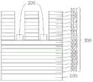
100-衬底层;200-电极单元;300-调制层单元;301-第一单元层;302-第二单元层;303-第三单元层;304-第四单元层;305-第五单元层;306-第六单元层;307-第七单元层;308-第八单元层;309-第九单元层;310-第十单元层;311-第十一单元层;312-第十二单元层;313-第十三单元层;314-第十四单元层;315-第十五单元层;316-第十六单元层;317-第十七单元层。100-substrate layer; 200-electrode unit; 300-modulation layer unit; 301-first unit layer; 302-second unit layer; 303-third unit layer; 304-fourth unit layer; 305-fifth unit layer ;306-sixth unit floor; 307-seventh unit floor; 308-eighth unit floor; 309-ninth unit floor; 310-tenth unit floor; 311-eleventh unit floor; 312-twelfth unit 313-thirteenth unit floor; 314-fourteenth unit floor; 315-fifteenth unit floor; 316-sixteenth unit floor; 317-seventeenth unit floor.
具体实施方式Detailed ways
本公开提供了一种空间光调制器及其制备方法,通过采用调制电极改变调制层的光学性质,进而实现对光波的调制,相较于液晶空间光调制器,因为采用了使用无机物作为固体状态的调制层和电极单元,具有插入损耗低、调制速度高、稳定性高和使用寿命长的特点。制备时可以实现加工步骤少、加工难度低、成品率高,所以生产成本低的有益效果。The present disclosure provides a spatial light modulator and a preparation method thereof. By using modulation electrodes to change the optical properties of the modulation layer, the modulation of light waves is realized. Compared with liquid crystal spatial light modulators, because inorganic substances are used as solid The state modulation layer and electrode unit have the characteristics of low insertion loss, high modulation speed, high stability and long service life. During the preparation, the beneficial effects of less processing steps, low processing difficulty, high yield and low production cost can be realized.
为使本公开的目的、技术方案和优点更加清楚明白,以下结合具体实施例,并参照附图,对本公开进一步详细说明。In order to make the purpose, technical solutions and advantages of the present disclosure clearer, the present disclosure will be further described in detail below in conjunction with specific embodiments and with reference to the accompanying drawings.
在本公开实施例中,提供一种空间光调制器,结合图1和图2所示,所述空间光调制器,包括:In an embodiment of the present disclosure, a spatial light modulator is provided. As shown in FIG. 1 and FIG. 2 , the spatial light modulator includes:
调制层单元300,包括依次设置的不同折射率的第一调制层301、第二调制层302和第三调制层303;所述第二调制层302的折射率与所述第一调制层301和第三调制层303不同,所述第一调制层301、第二调制层302和第三调制层303中至少一个调制层设置有至少一个图形单元;The
电极单元200,包括正电极和负电极,位于所述图形单元的间隙之中,所述电极单元能够调节所述电极单元所接触的调制层所述第二调制层的光学性质。The
如图1所示,调制层单元300包括第一调制层301、第二调制层302和第三调制层303,第二调制层302位于第一调制层301和第三调制层303之间。第二调制层302的折射率与第一调制层301和第三调制层303不同。第三调制层303包括至少一个图形单元。As shown in FIG. 1 , the
电极单元200位于第二调制层302的上方并与之接触。电极单元200位于第三调制层303的图形单元的间隙之中。电极单元200包括正电极和负电极。The
具体地,调制层单元300为热光材料、电光材料、声光材料或磁光材料。具体地,调制层单元300为单晶材料、多晶材料或非晶材料。具体地,调制层单元300为导体、半导体或绝缘体。具体地,调制层单元300包括但不限于Si、Ge、ITO、AZO、ZnO、GaN、AlN、ZnS、SiC、AlP、GaP、Au、Ag、Pt、Ta2O5、SiO2、Si3N4和Al2O3材料。具体地,调制层单元300的厚度为10nm到1mm。Specifically, the
较佳地,第一调制层301为SiO2材料,厚度为0.5mm,折射率为1.5。第一调制层301同时起到衬底的作用。较佳地,第二调制层302为多晶Si材料,较佳地,第二调制层302的厚度为100nm,折射率为3.5。较佳地,第三调制层303为Ge材料,厚度为200nm,折射率为4.2。第一调制层301和第二调制层302的折射率差的绝对值为2,第二调制层302和第三调制层303的折射率差的绝对值为0.7,两种折射率差的绝对值不相等。Preferably, the
可以理解的是,入射光波在第二调制层内进行传播时,通过对第二调制层施加电场或热场,可以改变第二调制层的折射率和吸收系数,改变第一调制层301和第二调制层302的折射率差的绝对值、第二调制层302和第三调制层303的折射率差的绝对值,从而改变反射光光束之间的相位差、改变反射光光束之间的干涉条件,进而实现反射光信号强度的调制。It can be understood that when the incident light wave propagates in the second modulation layer, by applying an electric field or a thermal field to the second modulation layer, the refractive index and absorption coefficient of the second modulation layer can be changed, and the
具体地,所述图形单元具有不同的折射率;第三调制层303的图形单元包括但不限于立方体、长方体、圆柱和梯形锥体。较佳地,第三调制层303的图形单元为长方体。具体地,第三调制层303的图形单元的间隙为0.1nm到1mm。较佳地,长方体的间隙为5000nm。Specifically, the graphic units have different refractive indices; the graphic units of the
具体地,电极单元200为金属、合金和透明导电氧化物中的任意一种或任意多种。电极单元包括但不限于Ag、Cu、Au、Al、Pt、Ni、Cr、Ti和ITO材料,电极单元的厚度为10nm到2000nm。电极单元200为电阻率不大于5×10⁻⁷Ω·m且与第二调制层302的接触势垒不大于1.5eV的具有低电阻率和低接触势垒的材料。较佳地,电极单元为Au/Al材料,Al的厚度为50nm,Au的厚度为150nm。Al材料的电阻率为2.7×10-8Ω·m,Au材料的电阻率为2.4×10-8Ω·m。电极单元200包括正电极和负电极,具体地,正电极和负电极的间距为0.2nm到1mm。较佳地,正电极和负电极的间距为100μm。Specifically, the
该电极单元的作用是连接电源与第二调制层,对第二调制层产生热场或电场,从而对在第二调制层中传输的光进行调制。可以理解的是,低电阻率的材料具有高的导电性能,低的接触势垒有利于电流的传导。并且,金属材料的热导率高,有利于传热。The function of the electrode unit is to connect the power source and the second modulation layer, generate a thermal field or an electric field on the second modulation layer, and thus modulate the light transmitted in the second modulation layer. It can be understood that materials with low resistivity have high electrical conductivity, and a low contact barrier is conducive to the conduction of electric current. Moreover, the metal material has high thermal conductivity, which is beneficial to heat transfer.
具体地,正电极和第三调制层303的图形单元的间隙为0.05nm到5000nm,负电极和第三调制层303的图形单元的间隙为0.05nm到5000nm。较佳地,正电极和第三调制层303的图形单元的间隙为1000nm,负电极和第三调制层303的图形单元的间隙为1000nm。可以理解的是,电极单元位于图形单元的间隙,不是位于调制层之间,可以减少电极单元对于光的吸收损耗。Specifically, the gap between the positive electrode and the pattern unit of the
作为本公开实施例的一种可选的实施方式,第三调制层303的图形单元具有不同的折射率。第三调制层303的图形单元的材料包括Ge材料和Ta2O5材料。Ge材料的厚度为90nm的正整数倍,折射率为4.2。Ta2O5材料的厚度为180nm的正整数倍,折射率为2.1。可以理解的是,在不同区域设置不同折射率的图形单元可以实现对入射光波不同的调制效果,可以增加空间光调制器的灵活性。As an optional implementation manner of the embodiment of the present disclosure, the pattern units of the
作为本公开实施例的一种可选的实施方式,电极单元200位于第一调制层301、第二调制层302和第三调制层303的任意一层或每一层的上方并与之接触。通过对每一层调制层施加电场或热场,都能够对光波进行调制,可以增加空间光调制器的灵活性和应用的便捷性。As an optional implementation manner of the embodiment of the present disclosure, the
作为本公开实施例的一种可选的实施方式,具体地,调制层单元300包括至少三层调制层,任意相邻的两层调制层的折射率差的绝对值至少具有两种。电极单元200位于调制层的任意一层或每一层的上方并与之接触。通过调整调制层的数量,可以实现空间光调制器的插入损耗较低的性能。通过对每一层调制层施加电场或热场,都能够对光波进行调制,可以增加空间光调制器的灵活性和应用的便捷性。As an optional implementation manner of the embodiment of the present disclosure, specifically, the
图3示意性示出了本公开另一实施例的空间光调制器结构示意图。Fig. 3 schematically shows a structural diagram of a spatial light modulator according to another embodiment of the present disclosure.
根据本公开实施例的一种可选的实施方式,包括衬底层100、调制层单元300和电极单元200。An optional implementation manner according to an embodiment of the present disclosure includes a
调制层单元300包括17层,其中,任意相邻的两层调制层的折射率差的绝对值具有两种。第一调制层301位于衬底层100的上方,第二调制层302位于第一调制层301和第三调制层303之间,其他调制层按编号从小到大的顺序依次从下向上排列。第十调制层310到第十七调制层317包括至少一个图形单元。The
电极单元200位于第九调制层309的上方并与之接触。电极单元200位于第十调制层310到第十七调制层317的图形单元的间隙之中。电极单元200包括正电极和负电极。The
具体地,衬底层100为导体、半导体或绝缘体,衬底层包括但不限于Al、Si、SiO2和Al2O3材料。较佳地,衬底层100为单晶Si材料。具体地,衬底层的厚度为0.1mm到10mm。较佳地,该衬底层的厚度为0.5mm。该衬底层的主要作用是承载和便于集成。Specifically, the
较佳地,第九调制层309为多晶Si材料,较佳地,第九调制层309的厚度为100nm,折射率为3.5。较佳地,除第九调制层309之外的每一层偶数调制层为SiO2材料,厚度为270nm的正整数倍,折射率为1.4。较佳地,除第九调制层309之外的每一层奇数调制层为TiO2材料,厚度为200nm的正整数倍,折射率为1.9,任意相邻偶数调制层和奇数调制层的折射率差的绝对值为0.5。第九调制层和相邻的调制层的折射率差的绝对值为的2.1。第九调制层309的作用是对光波进行调制,除第九调制层309之外的其它调制层的作用是对波长1550nm的光波进行高度反射。较佳地,第一调制层301到第八调制层308对1550nm波长光波的反射率为85%,第十调制层310到第十七调制层317对1550nm波长光波的反射率为85%。可以理解的是,在第九调制层下方增加其它调制层,其它调制层采用致密的绝缘体材料,能起到降低光的散射损耗的作用,从而降低空间光调制器的插入损耗。Preferably, the
根据本公开的一些实施例,空间光调制器对1550nm波长光波的反射率为90%,对1550nm波长光波的插入损耗为0.5dB,低于现有技术中液晶空间光调制器的插入损耗(1.5dB),比现有技术中液晶空间光调制器的插入损耗降低了三分之二。本公开的空间光调制器的调制速度在兆赫兹量级,比现有技术中液晶空间光调制器的调制速度(百赫兹量级)高4个量级。因此,本公开公开的空间光调制器相较于现有技术中的液晶空间光调制器,具有插入损耗低和调制速度高的特点。According to some embodiments of the present disclosure, the reflectivity of the spatial light modulator for light waves with a wavelength of 1550nm is 90%, and the insertion loss for light waves with a wavelength of 1550nm is 0.5dB, which is lower than the insertion loss (1.5 dB) of liquid crystal spatial light modulators in the prior art. dB), the insertion loss of the liquid crystal spatial light modulator in the prior art is reduced by two-thirds. The modulation speed of the spatial light modulator of the present disclosure is on the order of megahertz, which is 4 orders of magnitude higher than that of the liquid crystal spatial light modulator in the prior art (on the order of one hundred hertz). Therefore, compared with the liquid crystal spatial light modulator in the prior art, the spatial light modulator disclosed in the present disclosure has the characteristics of low insertion loss and high modulation speed.
根据本公开的一些实施例,衬底层100、调制层单元300和电极单元200都是固体,且衬底层100、调制层单元300和电极单元200都是无机物。无机物固体的使用温度通常高于液晶等有机物,具有使用温度高的优点。同时,无机物固体的抗老化性通常高于有机物,具有使用寿命长的优点,并且,衬底层100、调制层单元300和电极单元200的位置及相对位置均为固定不可变的,因此,本公开公开的空间光调制器相较于现有技术中的液晶空间光调制器,具有稳定性高和使用寿命长的特点。According to some embodiments of the present disclosure, the
图4示意性示出了本公开实施例的空间光调制器的制备方法的流程图。Fig. 4 schematically shows a flowchart of a method for manufacturing a spatial light modulator according to an embodiment of the present disclosure.
如图4所述,本公开还公开了一种空间光调制器的制备方法,包括:As shown in Figure 4, the present disclosure also discloses a method for preparing a spatial light modulator, including:
操作S1:在衬底100上方依次制备多层调制层得到调制层单元300;如图3所示,在衬底层100上方制备调制层单元300,依次制备第一调制层301到第十七调制层317;Operation S1: sequentially prepare multiple modulation layers on the
操作S2:对需要图形化的调制层进行图形化得到图形单元;Operation S2: Graphicalize the modulation layer that needs to be patterned to obtain a graphic unit;
如图3所示,对调制层单元300进行图形化,对需要图形化的第十调制层310到第十七调制层317进行图形化得到图形单元;As shown in FIG. 3 , the
操作S3:在所述图形单元的间隙制备电极单元;Operation S3: preparing electrode units between the pattern units;
如图3所示,在图形化单元的间隙中制备电极单元200,电极单元200位于第九调制层309上。As shown in FIG. 3 , an
操作S4:对电极单元200进行图形化,完成空间光调制器的制备。Operation S4: patterning the
根据本公开的一些实施例,将调制层单元300进行图形化之前还包括,将电极接触的第九调制层309的下表面进行减薄和抛光,将第九调制层309的下表面和第八调制层308的上表面进行键合。According to some embodiments of the present disclosure, before patterning the
根据本公开的一些实施例,制备调制层单元300和制备电极单元200时采用物理法或化学法;物理法包括以下之一:磁控溅射法、离子束溅射法、电子束蒸发法、热蒸发法或分子束外延法;化学法包括以下之一:化学气相沉积法、电化学法、溶胶凝胶法或水热法。制备所述调制层和制备所述电极单元包括沉积法或键合法;图形化的工艺方法包括光刻和刻蚀。According to some embodiments of the present disclosure, a physical method or a chemical method is used to prepare the
根据本公开的一些实施例,本公开公开的空间光调制器的制备方法包括2次沉积和2次图形化,共4个小步骤,远远地少于现有技术中液晶空间光调制器的加工步骤(24个),因此,本公开公开的空间光调制器的制备方法简化了加工工艺,提高了生产效率,降低了生产成本。According to some embodiments of the present disclosure, the manufacturing method of the spatial light modulator disclosed in the present disclosure includes 2 times of deposition and 2 times of patterning, a total of 4 small steps, which is far less than that of the liquid crystal spatial light modulator in the prior art There are 24 processing steps. Therefore, the manufacturing method of the spatial light modulator disclosed in the present disclosure simplifies the processing technology, improves the production efficiency, and reduces the production cost.
另外,本公开公开的空间光调制器的制备方法只包括沉积和图形化等加工难度较低的工艺,图形化的次数较少、对准偏差较小,不存在接触孔和封框胶的制备,具有加工难度低的优点,进一步降低了成产成本和提高了生产效率。In addition, the manufacturing method of the spatial light modulator disclosed in the present disclosure only includes processes such as deposition and patterning with low processing difficulty, the number of patterning is small, the alignment deviation is small, and there is no preparation of contact holes and sealing glue , has the advantages of low processing difficulty, further reduces the production cost and improves the production efficiency.
通过本公开公开的空间光调制器的制备方法生产空间光调制器的成品率可以高达90%,相较于现有技术中液晶空间光调制器的成品率27%,提高了产率,降低了损耗与成本。The yield of the spatial light modulator produced by the preparation method of the spatial light modulator disclosed in the present disclosure can be as high as 90%. Compared with the yield of 27% of the liquid crystal spatial light modulator in the prior art, the yield is improved and the loss and cost.
本公开公开的空间光调制器的调制机理为:利用第九调制层309的光学性质的变化调制经过空间光调制器的光波的光学参量。采用入射光照射空间光调制器,通过电极单元200对第九调制层309施加某种能量(例如:电和热等)改变第九调制层309的光学性质(例如:折射率和吸收系数等),从而改变空间光调制器的反射光的光学参量(例如:相位和振幅等)。除第九调制层309之外的其它调制层的作用是对波长1550nm的光波进行高度反射,其它调制层采用致密的绝缘体材料,能起到降低光的散射损耗的作用,从而降低空间光调制器的插入损耗。The modulation mechanism of the spatial light modulator disclosed in the present disclosure is: using the change of the optical properties of the
通过上述技术方案,通过采用调制电极改变调制层的光学性质,进而实现对光波的调制,相较于液晶空间光调制器,同时,因为采用了使用无机物作为固体状态的调制层和电极单元,本公开提供的空间光调制器具有插入损耗低、调制速度高、稳定性高和使用寿命长的特点。利用所述空间光调制器的所述制备方法可以实现加工步骤少、加工难度低、成品率高,所以生产成本低的有益效果。Through the above-mentioned technical scheme, the optical properties of the modulation layer are changed by using the modulation electrode, and then the modulation of the light wave is realized. Compared with the liquid crystal spatial light modulator, at the same time, because the modulation layer and the electrode unit using inorganic substances as solid state are used, The spatial light modulator provided by the present disclosure has the characteristics of low insertion loss, high modulation speed, high stability and long service life. Using the preparation method of the spatial light modulator can realize the beneficial effects of less processing steps, low processing difficulty, high yield and low production cost.
至此,已经结合附图对本公开实施例进行了详细描述。需要说明的是,在附图或说明书正文中,未绘示或描述的实现方式,均为所属技术领域中普通技术人员所知的形式,并未进行详细说明。此外,上述对各元件和方法的定义并不仅限于实施例中提到的各种具体结构、形状或方式,本领域普通技术人员可对其进行简单地更改或替换。So far, the embodiments of the present disclosure have been described in detail with reference to the accompanying drawings. It should be noted that, in the accompanying drawings or in the text of the specification, implementations that are not shown or described are forms known to those of ordinary skill in the art, and are not described in detail. In addition, the above definitions of each element and method are not limited to the various specific structures, shapes or methods mentioned in the embodiments, and those skilled in the art can easily modify or replace them.
依据以上描述,本领域技术人员应当对本公开空间光调制器及其制备方法有了清楚的认识。Based on the above description, those skilled in the art should have a clear understanding of the disclosed spatial light modulator and its manufacturing method.
综上所述,本公开提供了一种空间光调制器及其制备方法,在衬底上方依次制备各层调制层、对需要接触电极的每层调制层的上方的所有调制层进行图形化、在调制层的上方制备电极层和对电极层进行图形化,得到的空间光调制器具有插入损耗低和调制速度高的特点。上述制备方法相较于制备液晶空间光调制器,具有加工步骤少、加工难度低、成品率高,所以生产成本低的有益效果。In summary, the present disclosure provides a spatial light modulator and a manufacturing method thereof, in which various modulation layers are sequentially prepared above a substrate, and all modulation layers above each modulation layer that need to be in contact with electrodes are patterned, The electrode layer is prepared on the modulation layer and the electrode layer is patterned, and the obtained spatial light modulator has the characteristics of low insertion loss and high modulation speed. Compared with the preparation of the liquid crystal spatial light modulator, the above preparation method has the beneficial effects of less processing steps, low processing difficulty, high yield and low production cost.
还需要说明的是,实施例中提到的方向用语,例如“上”、“下”、“前”、“后”、“左”、“右”等,仅是参考附图的方向,并非用来限制本公开的保护范围。贯穿附图,相同的元素由相同或相近的附图标记来表示。在可能导致对本公开的理解造成混淆时,将省略常规结构或构造。It should also be noted that the directional terms mentioned in the embodiments, such as "up", "down", "front", "back", "left", "right", etc., are only referring to the directions of the drawings, not Used to limit the protection scope of this disclosure. Throughout the drawings, the same elements are indicated by the same or similar reference numerals. Conventional structures or constructions are omitted when they may obscure the understanding of the present disclosure.
并且图中各部件的形状和尺寸不反映真实大小和比例,而仅示意本公开实施例的内容。另外,在权利要求中,不应将位于括号之间的任何参考符号构造成对权利要求的限制。And the shape and size of each component in the figure do not reflect the actual size and proportion, but only illustrate the content of the embodiment of the present disclosure. Furthermore, in the claims, any reference signs placed between parentheses shall not be construed as limiting the claim.
再者,单词“包含”不排除存在未列在权利要求中的元件或步骤。位于元件之前的单词“一”或“一个”不排除存在多个这样的元件。Furthermore, the word "comprising" does not exclude the presence of elements or steps not listed in a claim. The word "a" or "an" preceding an element does not exclude the presence of a plurality of such elements.
说明书与权利要求中所使用的序数例如“第一”、“第二”、“第三”等的用词,以修饰相应的元件,其本身并不意味着该元件有任何的序数,也不代表某一元件与另一元件的顺序、或是制造方法上的顺序,该些序数的使用仅用来使具有某命名的一元件得以和另一具有相同命名的元件能做出清楚区分。Words such as "first", "second", "third" and the like used in the description and claims to modify the corresponding elements do not in themselves mean that the elements have any ordinal numbers, nor The use of these ordinal numbers to represent the sequence of an element with respect to another element, or the order of manufacturing methods, is only used to clearly distinguish one element with a certain designation from another element with the same designation.
此外,除非特别描述或必须依序发生的步骤,上述步骤的顺序并无限制于以上所列,且可根据所需设计而变化或重新安排。并且上述实施例可基于设计及可靠度的考虑,彼此混合搭配使用或与其他实施例混合搭配使用,即不同实施例中的技术特征可以自由组合形成更多的实施例。In addition, unless specifically described or steps that must occur sequentially, the order of the above steps is not limited to that listed above and may be changed or rearranged according to the desired design. Moreover, the above-mentioned embodiments can be mixed and matched with each other or with other embodiments based on design and reliability considerations, that is, technical features in different embodiments can be freely combined to form more embodiments.
本领域那些技术人员可以理解,可以对实施例中的设备中的模块进行自适应性地改变并且把它们设置在与该实施例不同的一个或多个设备中。可以把实施例中的模块或单元或组件组合成一个模块或单元或组件,以及此外可以把它们分成多个子模块或子单元或子组件。除了这样的特征和/或过程或者单元中的至少一些是相互排斥之外,可以采用任何组合对本说明书(包括伴随的权利要求、摘要和附图)中公开的所有特征以及如此公开的任何方法或者设备的所有过程或单元进行组合。除非另外明确陈述,本说明书(包括伴随的权利要求、摘要和附图)中公开的每个特征可以由提供相同、等同或相似目的的替代特征来代替。并且,在列举了若干装置的单元权利要求中,这些装置中的若干个可以是通过同一个硬件项来具体体现。Those skilled in the art can understand that the modules in the device in the embodiment can be adaptively changed and arranged in one or more devices different from the embodiment. Modules or units or components in the embodiments may be combined into one module or unit or component, and furthermore may be divided into a plurality of sub-modules or sub-units or sub-assemblies. All features disclosed in this specification (including accompanying claims, abstract and drawings) and any method or method so disclosed may be used in any combination, except that at least some of such features and/or processes or units are mutually exclusive. All processes or units of equipment are combined. Each feature disclosed in this specification (including accompanying claims, abstract and drawings) may be replaced by alternative features serving the same, equivalent or similar purpose, unless expressly stated otherwise. Moreover, in a unit claim enumerating several means, several of these means may be embodied by the same item of hardware.
以上所述的具体实施例,对本公开的目的、技术方案和有益效果进行了进一步详细说明,所应理解的是,以上所述仅为本公开的具体实施例而已,并不用于限制本公开,凡在本公开的精神和原则之内,所做的任何修改、等同替换、改进等,均应包含在本公开的保护范围之内。The specific embodiments described above further describe the purpose, technical solutions and beneficial effects of the present disclosure in detail. It should be understood that the above descriptions are only specific embodiments of the present disclosure, and are not intended to limit the present disclosure. Any modifications, equivalent replacements, improvements, etc. made within the spirit and principles of the present disclosure shall be included within the protection scope of the present disclosure.
Claims (9)
Translated fromChinesePriority Applications (1)
| Application Number | Priority Date | Filing Date | Title |
|---|---|---|---|
| CN202110658175.1ACN113391471B (en) | 2021-06-11 | 2021-06-11 | Spatial light modulator and its preparation method |
Applications Claiming Priority (1)
| Application Number | Priority Date | Filing Date | Title |
|---|---|---|---|
| CN202110658175.1ACN113391471B (en) | 2021-06-11 | 2021-06-11 | Spatial light modulator and its preparation method |
Publications (2)
| Publication Number | Publication Date |
|---|---|
| CN113391471A CN113391471A (en) | 2021-09-14 |
| CN113391471Btrue CN113391471B (en) | 2023-04-14 |
Family
ID=77620869
Family Applications (1)
| Application Number | Title | Priority Date | Filing Date |
|---|---|---|---|
| CN202110658175.1AActiveCN113391471B (en) | 2021-06-11 | 2021-06-11 | Spatial light modulator and its preparation method |
Country Status (1)
| Country | Link |
|---|---|
| CN (1) | CN113391471B (en) |
Families Citing this family (2)
| Publication number | Priority date | Publication date | Assignee | Title |
|---|---|---|---|---|
| CN114047651B (en)* | 2021-11-17 | 2022-11-08 | 中国科学院半导体研究所 | Spatial light modulator and method for manufacturing the same |
| CN116909043A (en)* | 2023-06-26 | 2023-10-20 | 中国科学院半导体研究所 | Spatial light modulator and preparation method thereof |
Family Cites Families (5)
| Publication number | Priority date | Publication date | Assignee | Title |
|---|---|---|---|---|
| JP5054639B2 (en)* | 2008-09-01 | 2012-10-24 | 日本放送協会 | Light modulator and spatial light modulator |
| JP2011180355A (en)* | 2010-03-01 | 2011-09-15 | Nippon Hoso Kyokai <Nhk> | Optical modulation element and spatial light modulator |
| CN104570402B (en)* | 2013-10-12 | 2018-05-29 | 中国科学院苏州纳米技术与纳米仿生研究所 | Spatial light modulator based on metamaterial structure and preparation method thereof |
| JP2017156555A (en)* | 2016-03-02 | 2017-09-07 | 日本放送協会 | Multistage light modulator and spatial light modulator |
| CN112596281B (en)* | 2020-12-17 | 2022-12-23 | 中国科学院半导体研究所 | Spatial light modulator and method of making the same |
- 2021
- 2021-06-11CNCN202110658175.1Apatent/CN113391471B/enactiveActive
Also Published As
| Publication number | Publication date |
|---|---|
| CN113391471A (en) | 2021-09-14 |
Similar Documents
| Publication | Publication Date | Title |
|---|---|---|
| CN108279511A (en) | A kind of electrooptic modulator based on phase-change material | |
| CN113391471B (en) | Spatial light modulator and its preparation method | |
| CN114047651B (en) | Spatial light modulator and method for manufacturing the same | |
| CN210720940U (en) | A liquid crystal box, liquid crystal antenna unit and liquid crystal phased array antenna | |
| CN112596281B (en) | Spatial light modulator and method of making the same | |
| CN107894669B (en) | Hybrid integrated optical modulator with graphene lithium niobate multilayer structure and preparation method thereof | |
| CN105700266B (en) | A kind of surface plasmons electric absorption optical modulator based on graphene | |
| CN105044929A (en) | Thermo-optic modulator based on graphene micro-ring structure and manufacturing method thereof | |
| CN115032819B (en) | Co-packaged light engine system and silicon-based modulator of phase change material array therefor | |
| CN102393550A (en) | Dimming delay line for silica delay and manufacturing method thereof | |
| CN115047655A (en) | Electro-optical modulation device based on micro electric heater and manufacturing method thereof | |
| CN111856783A (en) | Optical device and method of making the same | |
| CN113359330A (en) | Sinking electrode lithium niobate thin film electro-optical modulator and preparation method thereof | |
| CN113933931A (en) | A ring cavity light modulator based on vanadium dioxide nanowires | |
| CN110147000A (en) | An organic polymer optical waveguide absorption optical modulator based on buried graphene electrodes | |
| CN116009284A (en) | Micro optical switch unit based on double-hole GST phase change material and design method | |
| CN114005932A (en) | Controllable super-surface structure based on phase-change material and preparation method thereof | |
| WO2025060546A1 (en) | Optical modulator | |
| CN210427998U (en) | A metal nanoantenna-enhanced ultracompact graphene electro-optic modulator | |
| CN116400522B (en) | Thin film lithium niobate modulator with electrode layered climbing and its preparation method | |
| US20250261484A1 (en) | Micro-led chip, and preparation method and use thereof | |
| CN115712207A (en) | Silicon-based thermal modulation phase shifter based on transparent conductive oxide | |
| CN117250806A (en) | A lithium niobate film-sulfur series integrated chip on-chip acousto-optical control device and preparation method | |
| CN115167014A (en) | A C-band silicon-based modulator based on vanadium dioxide metamaterial structure | |
| CN109541822A (en) | A kind of graphene electro-optical modulator and preparation method thereof |
Legal Events
| Date | Code | Title | Description |
|---|---|---|---|
| PB01 | Publication | ||
| PB01 | Publication | ||
| SE01 | Entry into force of request for substantive examination | ||
| SE01 | Entry into force of request for substantive examination | ||
| GR01 | Patent grant | ||
| GR01 | Patent grant |