CN113327904B - A double-sided high-efficiency heat dissipation hermetic packaging structure and its preparation method - Google Patents
A double-sided high-efficiency heat dissipation hermetic packaging structure and its preparation methodDownload PDFInfo
- Publication number
- CN113327904B CN113327904BCN202110471099.3ACN202110471099ACN113327904BCN 113327904 BCN113327904 BCN 113327904BCN 202110471099 ACN202110471099 ACN 202110471099ACN 113327904 BCN113327904 BCN 113327904B
- Authority
- CN
- China
- Prior art keywords
- chip
- packaging substrate
- heat dissipation
- double
- substrate
- Prior art date
- Legal status (The legal status is an assumption and is not a legal conclusion. Google has not performed a legal analysis and makes no representation as to the accuracy of the status listed.)
- Active
Links
- 238000004806packaging method and processMethods0.000titleclaimsabstractdescription110
- 230000017525heat dissipationEffects0.000titleclaimsabstractdescription59
- 238000002360preparation methodMethods0.000titleclaimsabstractdescription6
- 239000000758substrateSubstances0.000claimsabstractdescription105
- 239000007788liquidSubstances0.000claimsabstractdescription15
- 238000001816coolingMethods0.000claimsabstractdescription12
- 230000010354integrationEffects0.000claimsdescription17
- 239000000919ceramicSubstances0.000claimsdescription14
- XUIMIQQOPSSXEZ-UHFFFAOYSA-NSiliconChemical compound[Si]XUIMIQQOPSSXEZ-UHFFFAOYSA-N0.000claimsdescription12
- 239000002184metalSubstances0.000claimsdescription12
- 238000000034methodMethods0.000claimsdescription12
- 229910052710siliconInorganic materials0.000claimsdescription12
- 239000010703siliconSubstances0.000claimsdescription12
- 229910000679solderInorganic materials0.000claimsdescription6
- 238000003466weldingMethods0.000claimsdescription4
- SWPMTVXRLXPNDP-UHFFFAOYSA-N4-hydroxy-2,6,6-trimethylcyclohexene-1-carbaldehydeChemical compoundCC1=C(C=O)C(C)(C)CC(O)C1SWPMTVXRLXPNDP-UHFFFAOYSA-N0.000claimsdescription3
- 238000004519manufacturing processMethods0.000claimsdescription2
- 238000007789sealingMethods0.000claimsdescription2
- 238000004377microelectronicMethods0.000abstractdescription2
- 238000005516engineering processMethods0.000description6
- 238000010586diagramMethods0.000description2
- 238000009826distributionMethods0.000description2
- 230000004907fluxEffects0.000description2
- 230000008054signal transmissionEffects0.000description2
- 230000002159abnormal effectEffects0.000description1
- 230000009286beneficial effectEffects0.000description1
- 239000000969carrierSubstances0.000description1
- 238000001312dry etchingMethods0.000description1
- 238000003475laminationMethods0.000description1
- 238000005457optimizationMethods0.000description1
- 238000000206photolithographyMethods0.000description1
- 238000005245sinteringMethods0.000description1
Images


Classifications
- H—ELECTRICITY
- H01—ELECTRIC ELEMENTS
- H01L—SEMICONDUCTOR DEVICES NOT COVERED BY CLASS H10
- H01L23/00—Details of semiconductor or other solid state devices
- H01L23/34—Arrangements for cooling, heating, ventilating or temperature compensation ; Temperature sensing arrangements
- H01L23/46—Arrangements for cooling, heating, ventilating or temperature compensation ; Temperature sensing arrangements involving the transfer of heat by flowing fluids
- H01L23/473—Arrangements for cooling, heating, ventilating or temperature compensation ; Temperature sensing arrangements involving the transfer of heat by flowing fluids by flowing liquids
- B—PERFORMING OPERATIONS; TRANSPORTING
- B81—MICROSTRUCTURAL TECHNOLOGY
- B81B—MICROSTRUCTURAL DEVICES OR SYSTEMS, e.g. MICROMECHANICAL DEVICES
- B81B1/00—Devices without movable or flexible elements, e.g. microcapillary devices
- B—PERFORMING OPERATIONS; TRANSPORTING
- B81—MICROSTRUCTURAL TECHNOLOGY
- B81C—PROCESSES OR APPARATUS SPECIALLY ADAPTED FOR THE MANUFACTURE OR TREATMENT OF MICROSTRUCTURAL DEVICES OR SYSTEMS
- B81C1/00—Manufacture or treatment of devices or systems in or on a substrate
- B81C1/00015—Manufacture or treatment of devices or systems in or on a substrate for manufacturing microsystems
- B81C1/00023—Manufacture or treatment of devices or systems in or on a substrate for manufacturing microsystems without movable or flexible elements
- B81C1/00055—Grooves
- B81C1/00063—Trenches
- B—PERFORMING OPERATIONS; TRANSPORTING
- B81—MICROSTRUCTURAL TECHNOLOGY
- B81C—PROCESSES OR APPARATUS SPECIALLY ADAPTED FOR THE MANUFACTURE OR TREATMENT OF MICROSTRUCTURAL DEVICES OR SYSTEMS
- B81C1/00—Manufacture or treatment of devices or systems in or on a substrate
- B81C1/00015—Manufacture or treatment of devices or systems in or on a substrate for manufacturing microsystems
- B81C1/00023—Manufacture or treatment of devices or systems in or on a substrate for manufacturing microsystems without movable or flexible elements
- B81C1/00055—Grooves
- B81C1/00071—Channels
- H—ELECTRICITY
- H01—ELECTRIC ELEMENTS
- H01L—SEMICONDUCTOR DEVICES NOT COVERED BY CLASS H10
- H01L21/00—Processes or apparatus adapted for the manufacture or treatment of semiconductor or solid state devices or of parts thereof
- H01L21/02—Manufacture or treatment of semiconductor devices or of parts thereof
- H01L21/04—Manufacture or treatment of semiconductor devices or of parts thereof the devices having potential barriers, e.g. a PN junction, depletion layer or carrier concentration layer
- H01L21/48—Manufacture or treatment of parts, e.g. containers, prior to assembly of the devices, using processes not provided for in a single one of the groups H01L21/18 - H01L21/326 or H10D48/04 - H10D48/07
- H01L21/4814—Conductive parts
- H01L21/4871—Bases, plates or heatsinks
- H01L21/4882—Assembly of heatsink parts
- H—ELECTRICITY
- H01—ELECTRIC ELEMENTS
- H01L—SEMICONDUCTOR DEVICES NOT COVERED BY CLASS H10
- H01L23/00—Details of semiconductor or other solid state devices
- H01L23/34—Arrangements for cooling, heating, ventilating or temperature compensation ; Temperature sensing arrangements
- H01L23/36—Selection of materials, or shaping, to facilitate cooling or heating, e.g. heatsinks
- H01L23/367—Cooling facilitated by shape of device
- H—ELECTRICITY
- H01—ELECTRIC ELEMENTS
- H01L—SEMICONDUCTOR DEVICES NOT COVERED BY CLASS H10
- H01L23/00—Details of semiconductor or other solid state devices
- H01L23/34—Arrangements for cooling, heating, ventilating or temperature compensation ; Temperature sensing arrangements
- H01L23/36—Selection of materials, or shaping, to facilitate cooling or heating, e.g. heatsinks
- H01L23/373—Cooling facilitated by selection of materials for the device or materials for thermal expansion adaptation, e.g. carbon
- H01L23/3731—Ceramic materials or glass
- H—ELECTRICITY
- H01—ELECTRIC ELEMENTS
- H01L—SEMICONDUCTOR DEVICES NOT COVERED BY CLASS H10
- H01L23/00—Details of semiconductor or other solid state devices
- H01L23/34—Arrangements for cooling, heating, ventilating or temperature compensation ; Temperature sensing arrangements
- H01L23/46—Arrangements for cooling, heating, ventilating or temperature compensation ; Temperature sensing arrangements involving the transfer of heat by flowing fluids
- H01L23/467—Arrangements for cooling, heating, ventilating or temperature compensation ; Temperature sensing arrangements involving the transfer of heat by flowing fluids by flowing gases, e.g. air
- H—ELECTRICITY
- H01—ELECTRIC ELEMENTS
- H01L—SEMICONDUCTOR DEVICES NOT COVERED BY CLASS H10
- H01L23/00—Details of semiconductor or other solid state devices
- H01L23/552—Protection against radiation, e.g. light or electromagnetic waves
- H—ELECTRICITY
- H01—ELECTRIC ELEMENTS
- H01L—SEMICONDUCTOR DEVICES NOT COVERED BY CLASS H10
- H01L25/00—Assemblies consisting of a plurality of semiconductor or other solid state devices
- H01L25/16—Assemblies consisting of a plurality of semiconductor or other solid state devices the devices being of types provided for in two or more different subclasses of H10B, H10D, H10F, H10H, H10K or H10N, e.g. forming hybrid circuits
Landscapes
- Engineering & Computer Science (AREA)
- Microelectronics & Electronic Packaging (AREA)
- Computer Hardware Design (AREA)
- Physics & Mathematics (AREA)
- Condensed Matter Physics & Semiconductors (AREA)
- General Physics & Mathematics (AREA)
- Power Engineering (AREA)
- Manufacturing & Machinery (AREA)
- Chemical & Material Sciences (AREA)
- Analytical Chemistry (AREA)
- Materials Engineering (AREA)
- Health & Medical Sciences (AREA)
- Electromagnetism (AREA)
- Toxicology (AREA)
- Ceramic Engineering (AREA)
- Cooling Or The Like Of Semiconductors Or Solid State Devices (AREA)
Abstract
Description
Translated fromChinese技术领域technical field
本发明涉及微电子散热技术领域,具体的,涉及一种双面高效散热气密封装结构及其制备方法。The invention relates to the technical field of microelectronic heat dissipation, in particular to a double-sided high-efficiency heat dissipation airtight packaging structure and a preparation method thereof.
背景技术Background technique
为满足电子设备高密度、高性能、高可靠的应用需求,微波组件的封装结构持续向着小型化、高集成度、高气密性的方向发展。传统平面集成的方式已经不能满足要求,需要将元器件在封装基板上双面集成,在相同的面积下,实现集成密度提升一倍。此外,由于GaN微波功率技术的逐渐成熟,功率芯片的功率密度逐渐提升,其热流密度也随之提升。普通的被动散热技术已经不能满足微波组件的散热需求,需要采用更高效的微流体增强散热技术。In order to meet the high-density, high-performance, and high-reliability application requirements of electronic equipment, the packaging structure of microwave components continues to develop in the direction of miniaturization, high integration, and high airtightness. The traditional planar integration method can no longer meet the requirements. It is necessary to integrate the components on both sides of the package substrate, and achieve double the integration density under the same area. In addition, due to the gradual maturity of GaN microwave power technology, the power density of power chips has gradually increased, and its heat flux has also increased. Ordinary passive heat dissipation technology can no longer meet the heat dissipation requirements of microwave components, and more efficient microfluidic enhanced heat dissipation technology is required.
现有关于高效散热结构和双面封装结构的专利很多:如中国专利ZL201810601226.5提出了一种基于硅基微流道和多腔槽结构实现大功率GaN器件散热的封装方法,实现了面向微波应用的高密度集成;然而,该专利基于硅基板集成,技术难度大,中小批量加工时成本高。又如中国专利202010160541.6提出了一种LTCC基板双面腔体结构的制作方法;然而,该专利并没有涉及LTCC基板内嵌微流道,以及LTCC微流道与硅基微流道的一体化集成,不能解决功率芯片的高效散热问题。There are many existing patents on high-efficiency heat dissipation structures and double-sided packaging structures: for example, Chinese patent ZL201810601226.5 proposes a packaging method for heat dissipation of high-power GaN devices based on silicon-based microfluidic channels and multi-cavity groove structures, realizing microwave-oriented High-density integration of applications; however, this patent is based on silicon substrate integration, which is technically difficult and costly for small and medium batch processing. Another example is Chinese patent 202010160541.6, which proposes a method for manufacturing a double-sided cavity structure on an LTCC substrate; however, this patent does not involve microchannels embedded in LTCC substrates, and the integrated integration of LTCC microchannels and silicon-based microchannels , can not solve the problem of efficient heat dissipation of power chips.
如何构建面向典型微波多芯片组件应用的双面高效散热气密封装结构,在实现高热流密度散热的同时,满足组件气密封装和微波信号电磁兼容性要求,目前还鲜有报道。How to construct a double-sided high-efficiency heat-dissipating hermetic packaging structure for typical microwave multi-chip module applications, while achieving high heat flux dissipation and meeting the requirements of hermetic packaging of components and electromagnetic compatibility of microwave signals, is still rarely reported.
发明内容Contents of the invention
本发明所要解决的问题是:针对现有技术存在的问题,本发明提供一种双面高效散热气密封装结构及其制备方法,在满足封装结构气密性的前提下,实现大功率芯片高效散热、中小功率芯片有效散热,最终实现封装内热量均匀分布,同时满足微波信号传输的电磁兼容性要求。The problem to be solved by the present invention is: Aiming at the problems existing in the prior art, the present invention provides a double-sided high-efficiency heat-dissipating hermetic packaging structure and its preparation method, which can realize high-efficiency high-power chips on the premise of satisfying the airtightness of the packaging structure. Heat dissipation, effective heat dissipation of small and medium power chips, and finally achieve uniform heat distribution in the package, while meeting the electromagnetic compatibility requirements of microwave signal transmission.
本发明采用的技术方案如下: 一种双面高效散热气密封装结构,包括:散热微流道、封装基板、第一芯片、第二芯片、围框、盖板一、盖板二、液冷连接器和电连接器;The technical solution adopted by the present invention is as follows: A double-sided high-efficiency heat-dissipating hermetic packaging structure, including: heat-dissipating micro-channel, packaging substrate, first chip, second chip, surrounding frame, cover plate 1,
所述散热微流道和围框焊接在封装基板上;The heat dissipation micro-channel and the surrounding frame are welded on the packaging substrate;
所述第一芯片焊接在散热微流道上,第二芯片焊接在封装基板上,且第一芯片和第二芯片均与封装基板互联;The first chip is welded on the heat dissipation micro-channel, the second chip is welded on the packaging substrate, and both the first chip and the second chip are interconnected with the packaging substrate;
所述盖板一焊接在围框上,盖板二焊接在封装基板上;The first cover plate is welded on the surrounding frame, and the second cover plate is welded on the packaging substrate;
所述液冷连接器和电连接器焊接在封装基板底部。The liquid cooling connector and the electrical connector are welded on the bottom of the packaging substrate.
所述散热微流道为高效散热硅基微流道,其中的流道为小尺寸、高深宽比微流道,流道尺寸在10~100µm之间,流道深宽比≥5:1;微流体的散热能力与微流道的流道截面尺寸密切相关,流道的截面宽度越窄、深宽比越大,微流道的换热能力愈强;同时硅基MEMS加工工艺由于采用了光刻、干法刻蚀等微纳加工工艺,可以制备截面宽度为数十微米、深宽比大于5:1的高效散热微流道,实现局部高效散热,其高效散热能力为500W/cm2~1000W/cm2。The heat-dissipating microchannel is a high-efficiency heat-dissipating silicon-based microchannel, wherein the flow channel is a small-sized, high-aspect-ratio micro-channel, the channel size is between 10 and 100 µm, and the channel aspect ratio is ≥ 5:1; The heat dissipation capacity of microfluid is closely related to the cross-sectional size of the micro-channel. The narrower the cross-sectional width of the channel and the larger the aspect ratio, the stronger the heat transfer capacity of the micro-channel. At the same time, the silicon-based MEMS processing technology adopts the Photolithography, dry etching and other micro-nano processing techniques can prepare highly efficient heat dissipation microchannels with a cross-sectional width of tens of microns and an aspect ratio greater than 5:1 to achieve local efficient heat dissipation, and its high-efficiency heat dissipation capacity is 500W/cm2 ~1000W/cm2 .
所述第一芯片为大功率射频芯片,包括功率放大芯片和开关芯片;所述第二芯片为中小功率芯片,包括除大功率功率放大芯片和大功率开关芯片以外的其它所有芯片。The first chip is a high-power radio frequency chip, including a power amplifier chip and a switch chip; the second chip is a low-to-medium power chip, including all other chips except a high-power power amplifier chip and a high-power switch chip.
所述封装基板为内嵌微流道双面腔槽陶瓷封装基板,其中的流道为中小尺寸微流道,流道尺寸在100µm~3mm之间,流道深宽比≤3:1,该中小尺寸微流道用于第二芯片的普通散热,其普通散热能力为50W/cm2~150W/cm2。The packaging substrate is a ceramic packaging substrate with double-sided cavity grooves embedded in micro-channels, wherein the flow channels are small and medium-sized micro-channels, the size of the flow channels is between 100 μm and 3 mm, and the aspect ratio of the flow channels is ≤ 3:1. The small and medium-sized micro-channels are used for ordinary heat dissipation of the second chip, and their ordinary heat dissipation capacity is 50W/cm2 -150W/cm2 .
所述内嵌微流道双面腔槽陶瓷封装基板为LTCC或HTCC陶瓷封装基板,HTCC或LTCC陶瓷基板可以比较方便地在单块基板中实现毫米尺度的深腔槽,故可以在封装基板正反两面制备毫米尺度的腔槽,再与散热微流道一体化集成,实现功率第一芯片顶部需要保留高空气腔的需求。The embedded micro-channel double-sided cavity ceramic packaging substrate is an LTCC or HTCC ceramic packaging substrate, and the HTCC or LTCC ceramic substrate can easily realize millimeter-scale deep cavity grooves in a single substrate, so it can be used on the packaging substrate. Millimeter-scale cavity grooves are prepared on both sides, and then integrated with heat dissipation micro-channels to realize the need to retain a high-level air cavity on the top of the power-first chip.
所述封装基板的顶面有深腔槽,所述封装基板顶面深腔槽深度在1.5mm~3mm之间,所述封装基板顶面深腔槽用于集成散热微流道;所述封装基板的底面有矮腔槽,所述封装基板底面矮腔槽的深度在0.5mm~1mm之间,所述封装基板底面矮腔槽用于集成第二芯片。The top surface of the packaging substrate has a deep cavity groove, the depth of the deep cavity groove on the top surface of the packaging substrate is between 1.5 mm and 3 mm, and the deep cavity groove on the top surface of the packaging substrate is used for integrating heat dissipation micro-channels; the packaging The bottom surface of the substrate has a low-cavity groove, and the depth of the low-cavity groove on the bottom surface of the packaging substrate is between 0.5 mm and 1 mm, and the low-cavity groove on the bottom surface of the packaging substrate is used for integrating the second chip.
所述围框为金属围框;所述盖板一和盖板二均为金属盖板。The surrounding frame is a metal surrounding frame; the first cover plate and the second cover plate are both metal cover plates.
所述封装基板顶面深腔槽、围框和盖板一之间有气密高空气腔,气密高空气腔的高度在1mm~3mm之间;所述封装基板底面矮腔槽与盖板二之间有气密矮空气腔,气密矮空气腔的高度在0.5mm~1mm之间;在多芯片大功率微波组件中,功率放大芯片顶部需要保留1~3mm的高空气腔,其余芯片顶部需要保留数百微米的矮空气腔,防止出现芯片输出信号异常、自激和烧毁等现象。There is an airtight high air cavity between the deep cavity groove on the top surface of the packaging substrate, the surrounding frame and the cover plate, and the height of the airtight high air cavity is between 1mm and 3mm; the low cavity groove on the bottom surface of the packaging substrate and the cover plate There is an airtight low air cavity between the two, and the height of the airtight low air cavity is between 0.5mm and 1mm; in a multi-chip high-power microwave component, a high air cavity of 1 to 3mm needs to be reserved on the top of the power amplifier chip, and the other chips A short air cavity of hundreds of microns needs to be reserved on the top to prevent abnormal chip output signals, self-excitation, and burnout.
本发明还公开了一种双面高效散热气密封装结构的制备方法,包括以下步骤:The invention also discloses a method for preparing a double-sided high-efficiency heat-dissipating hermetic packaging structure, which includes the following steps:
步骤1:将散热微流道和围框气密焊接在封装基板顶面上;Step 1: Airtightly weld the heat dissipation microchannel and the surrounding frame on the top surface of the packaging substrate;
步骤2:通过低热阻集成的方式将第一芯片焊接在散热微流道上;Step 2: Solder the first chip on the heat dissipation microchannel through low thermal resistance integration;
步骤3:通过键合引线,将第一芯片和封装基板互联;Step 3: interconnecting the first chip and the packaging substrate through bonding wires;
步骤4:将盖板一焊接在围框上进行气密封盖;Step 4: Weld the cover plate to the frame for airtight sealing;
步骤5:将第二芯片通过低热阻集成的方法焊接在封装基板上;Step 5: Welding the second chip on the packaging substrate by means of low thermal resistance integration;
步骤6:再通过引键合引线,将第二芯片与封装基板互联;Step 6: interconnecting the second chip with the packaging substrate through bonding wires;
步骤7:利用盖板二对封装基板进行气密封盖,得到双面高效散热气密封装结构;Step 7: Use the
步骤8:将液冷连接器和电连接器焊接在封装基板上。Step 8: Solder the liquid cooling connector and the electrical connector on the package substrate.
与现有技术相比,采用上述技术方案的有益效果为:Compared with the prior art, the beneficial effects of adopting the above technical solution are:
(1)将高效散热硅基微流道与内嵌微流道双面腔槽陶瓷封装基板一体化集成。同步在封装基板顶面制备深腔槽,并结合金属围框和金属盖板实现高空气腔;在封装基板底面制备矮腔槽,并结合金属盖板实现矮空气腔。在满足封装结构气密性的前提下,同时满足微波信号传输的电磁兼容性要求。(1) Integrated high-efficiency heat-dissipating silicon-based microchannels and ceramic packaging substrates with embedded microchannels and double-sided cavities. Simultaneously prepare deep cavity grooves on the top surface of the packaging substrate, and combine the metal frame and metal cover to realize the high air cavity; prepare the low cavity groove on the bottom surface of the packaging substrate, and combine the metal cover to realize the low air cavity. On the premise of meeting the airtightness of the packaging structure, it also meets the electromagnetic compatibility requirements of microwave signal transmission.
(2)使用内嵌中小尺寸微流道的双面腔槽陶瓷封装基板作为分流网络和中小功率芯片的普通散热载体,可实现50W/cm2~150W/cm2的散热能力;使用内嵌小尺寸、高深宽比微流道的高效散热硅基微流道作为大功率射频芯片的高效散热载体,可实现500W/cm2~1000W/cm2的散热能力。分别优化设计两种流道的尺寸和结构后,将二者双面集成,实现大功率芯片高效散热、中小功率芯片有效散热,最终实现封装内热量均匀分布。(2) Using the double-sided cavity ceramic packaging substrate embedded with small and medium-sized micro-channels as a common heat dissipation carrier for the shunt network and small and medium-power chips can achieve a heat dissipation capacity of 50W/cm2 to 150W/cm2 ; High-efficiency heat-dissipating silicon-based micro-channels with large size and high aspect ratio micro-channels are used as high-efficiency heat dissipation carriers for high-power radio frequency chips, and can achieve a heat dissipation capacity of 500W/cm2 to 1000W/cm2 . After optimizing the size and structure of the two flow channels, they are double-sidedly integrated to achieve efficient heat dissipation for high-power chips, effective heat dissipation for small and medium-power chips, and finally achieve uniform heat distribution in the package.
(3)综合利用了硅基微纳加工工艺可制备小尺寸、高深宽比微流道和陶瓷基板叠层后烧结工艺可制备中小尺寸微流道、毫米尺度腔槽的技术优势,实现了成本、散热能力和微波性能的综合最优。(3) The silicon-based micro-nano processing technology can be used to prepare small-sized, high-aspect-ratio micro-channels and the technical advantages of ceramic substrate lamination and sintering technology can be used to prepare small and medium-sized micro-channels and millimeter-scale cavities. , comprehensive optimization of heat dissipation capacity and microwave performance.
(4)使用一块封装基板就可以实现更多元器件的双面集成,集成密度更高,集成工艺更加简单。(4) The double-sided integration of more components can be realized by using one packaging substrate, the integration density is higher, and the integration process is simpler.
附图说明Description of drawings
图1是本发明的剖面示意图。Fig. 1 is a schematic cross-sectional view of the present invention.
图2是本发明的散热微流道切面示意图。Fig. 2 is a schematic diagram of a sectional view of the heat dissipation microfluidic channel of the present invention.
图3是本发明的封装基板切面示意图。FIG. 3 is a schematic cross-sectional view of the packaging substrate of the present invention.
图4是本发明的制备方法工艺流程图。Fig. 4 is a process flow diagram of the preparation method of the present invention.
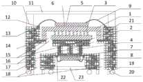
附图标记:1-散热微流道;2-封装基板;3-小尺寸、高深宽比微流道;4-中小尺寸微流道;5-第一芯片;6-第一芯片低热阻集成界面;7-第二芯片低热阻集成界面;8-第二芯片;9-键合引线;10-围框;11-盖板一;12-焊盘;13-封装基板内金属布线层;14-封装基板内金属通孔;15-进/出液口Ⅰ;16-进/出液口Ⅱ;17-分流网络;18-进/出液口Ⅲ;19-液冷连接器;20-电连接器;21-封装基板顶面深腔槽;22-封装基板底面矮腔槽;23-盖板二。Reference signs: 1-heat dissipation microchannel; 2-package substrate; 3-small size, high aspect ratio microchannel; 4-small and medium size microchannel; 5-first chip; 6-first chip low thermal resistance integration Interface; 7-second chip low thermal resistance integrated interface; 8-second chip; 9-bonding wire; 10-surrounding frame; 11-cover plate 1; 12-pad; 13-metal wiring layer in package substrate; 14 -Metal through hole in the package substrate; 15-inlet/outlet port I; 16-inlet/outlet port II; 17-shunt network; 18-inlet/outlet port III; 19-liquid cooling connector; 20-electricity Connector; 21-deep cavity groove on the top surface of the packaging substrate; 22-short cavity groove on the bottom surface of the packaging substrate; 23-cover plate two.
具体实施方式Detailed ways
下面结合附图对本发明作进一步描述。The present invention will be further described below in conjunction with the accompanying drawings.
如图1-图3所示,一种双面高效散热气密封装结构,包括:散热微流道1、封装基板2、第一芯片5、第二芯片8、围框10、盖板一11、盖板二23、液冷连接器19和电连接器20;As shown in Figures 1-3, a double-sided high-efficiency heat-dissipating hermetic packaging structure includes: a heat-dissipating microchannel 1, a
所述散热微流道1和围框10焊接在封装基板2上;The heat dissipation microchannel 1 and the surrounding
所述第一芯片5焊接在散热微流道1上,第二芯片8焊接在封装基板2上,且第一芯片5和第二芯片8均与封装基板2互联;The
所述盖板一11焊接在围框10上,盖板二23焊接在封装基板2上;The
所述液冷连接器19和电连接器20焊接在封装基板2底部。The
在一个优选的实施例中,所述散热微流道1为高效散热硅基微流道,其中的流道为小尺寸、高深宽比微流道3,流道尺寸为25µm,流道深宽比为10:1。In a preferred embodiment, the heat-dissipating microchannel 1 is an efficient heat-dissipating silicon-based microchannel, in which the flow channel is a small-sized, high-aspect-ratio micro-channel 3 with a channel size of 25 μm and a depth and width of the channel. The ratio is 10:1.
在一个优选的实施例中,所述散热微流道1的底部还设有进/出液口Ⅰ15。In a preferred embodiment, the bottom of the heat dissipation microchannel 1 is also provided with a liquid inlet/outlet I15.
在一个优选的实施例中,所述封装基板2为内嵌微流道双面腔槽陶瓷封装基板,所述内嵌微流道双面腔槽陶瓷封装基板,其中的流道尺寸为500um,流道深宽比为1:1。In a preferred embodiment, the
在一个优选的实施例中,所述封装基板2的顶面设有进/出液口Ⅱ16,底面设有进/出液口Ⅲ18;且封装基板中部设有中小尺寸微流道4,同时封装基板内部两侧还设有分流网络17。In a preferred embodiment, the top surface of the
在一个优选的实施例中,所述第一芯片5,包括功率放大芯片和开关芯片;所述第二芯片8,包括除大功率功率放大芯片和大功率开关芯片以外的其它所有芯片。In a preferred embodiment, the
在一个优选的实施例中,所述封装基板2的顶面有深腔槽,所述封装基板顶面深腔槽21深度在1.5mm~3mm之间,所述封装基板顶面深腔槽21用于集成散热微流道;所述封装基板2的底面有矮腔槽,所述封装基板底面矮腔槽22的深度在0.5mm~1mm之间,所述封装基板底面矮腔槽用于集成第二芯片。In a preferred embodiment, the top surface of the
在一个优选的实施例中,所述盖板一11、封装基板顶面深腔槽21和围框10之间形成了第一芯片5顶部2mm的气密高空气腔;所述封装基板底面矮腔槽22和盖板二23之间形成了第二芯片8顶部800um的气密矮空气腔。In a preferred embodiment, an airtight high air cavity of 2 mm at the top of the
需要说明的是,散热微流道1用于实现第一芯片600W/cm2的高效散热;封装基板2用于实现1个散热微流道的供液和第二芯片100W/cm2的普通散热。It should be noted that the heat dissipation microchannel 1 is used to realize the efficient heat dissipation of the first chip at 600W/cm2 ; the
需要说明的是,所述封装基板顶面深腔槽21上可集成1个或多个散热微流道。It should be noted that one or more heat dissipation micro-channels can be integrated in the
需要说明的是,该双面高效散热气密封装结构使用液冷连接器19和电连接器20对外互联。It should be noted that the double-sided high-efficiency heat-dissipating hermetic packaging structure uses a liquid-cooled
如图4所示,提供了一种上述双面高效散热气密封装结构的制备方法:As shown in Figure 4, a method for preparing the above-mentioned double-sided high-efficiency heat-dissipating hermetic packaging structure is provided:
步骤1:将散热微流道1和围框10气密焊接在封装基板2上;Step 1: Hermetically welding the heat dissipation micro-channel 1 and the surrounding
步骤2:通过低热阻集成的方式将第一芯片5焊接在散热微流道1上;Step 2: Solder the
步骤3:通过键合引线,将第一芯片5和封装基板2互联;Step 3: interconnecting the
步骤4:将盖板一11焊接在围框10上进行气密封盖;Step 4: Weld the
步骤5:将第二芯片8通过低热阻集成的方法焊接在封装基板2上;Step 5: Welding the
步骤6:再通过键合引线,将中小功率芯片8与封装基板2互联;Step 6: interconnecting the small and
步骤7:利用盖板二23对封装基板2进行焊接气密封盖,得到双面高效散热气密封装结构;Step 7: Use the
步骤8:将液冷连接器19和电连接器20焊接在封装基板上。Step 8: Solder the
本发明并不局限于前述的具体实施方式。本发明扩展到任何在本说明书中披露的新特征或任何新的组合,以及披露的任一新的方法或过程步骤或任何新的组合。如果本领域技术人员,在不脱离本发明的精神所做的非实质性改变或改进,都应该属于本发明权利要求保护的范围。The present invention is not limited to the foregoing specific embodiments. The invention extends to any novel feature or any novel combination disclosed in this specification, and to any new method or process step or any novel combination disclosed. Any insubstantial changes or improvements made by those skilled in the art without departing from the spirit of the present invention shall all fall within the protection scope of the claims of the present invention.
Claims (9)
Translated fromChinesePriority Applications (1)
| Application Number | Priority Date | Filing Date | Title |
|---|---|---|---|
| CN202110471099.3ACN113327904B (en) | 2021-04-29 | 2021-04-29 | A double-sided high-efficiency heat dissipation hermetic packaging structure and its preparation method |
Applications Claiming Priority (1)
| Application Number | Priority Date | Filing Date | Title |
|---|---|---|---|
| CN202110471099.3ACN113327904B (en) | 2021-04-29 | 2021-04-29 | A double-sided high-efficiency heat dissipation hermetic packaging structure and its preparation method |
Publications (2)
| Publication Number | Publication Date |
|---|---|
| CN113327904A CN113327904A (en) | 2021-08-31 |
| CN113327904Btrue CN113327904B (en) | 2023-06-02 |
Family
ID=77413919
Family Applications (1)
| Application Number | Title | Priority Date | Filing Date |
|---|---|---|---|
| CN202110471099.3AActiveCN113327904B (en) | 2021-04-29 | 2021-04-29 | A double-sided high-efficiency heat dissipation hermetic packaging structure and its preparation method |
Country Status (1)
| Country | Link |
|---|---|
| CN (1) | CN113327904B (en) |
Families Citing this family (5)
| Publication number | Priority date | Publication date | Assignee | Title |
|---|---|---|---|---|
| CN114256175B (en)* | 2021-12-07 | 2023-09-01 | 中国电子科技集团公司第二十九研究所 | Tile type TR (transmitter-receiver) component embedded in micro-channel and preparation method thereof |
| CN115175438B (en)* | 2022-07-04 | 2025-08-01 | 中国电子科技集团公司第二十九研究所 | Airtight packaging method of microwave assembly based on embedded micro-channel printed circuit board |
| CN115315064A (en)* | 2022-07-04 | 2022-11-08 | 中国电子科技集团公司第二十九研究所 | Hermetic packaging assembly based on embedded microfluidic printed circuit board and preparation method thereof |
| CN115602636B (en)* | 2022-11-02 | 2025-09-19 | 中国电子科技集团公司第二十九研究所 | Three-dimensional airtight packaging structure and packaging method |
| CN116190243B (en)* | 2022-11-14 | 2025-08-19 | 四川斯艾普电子科技有限公司 | Method for improving power capacity of thick film integrated radio frequency device and radio frequency device |
Citations (11)
| Publication number | Priority date | Publication date | Assignee | Title |
|---|---|---|---|---|
| JP2005322879A (en)* | 2004-04-06 | 2005-11-17 | Showa Denko Kk | Semiconductor device substrate, semiconductor module, and electric vehicle |
| CN101826494A (en)* | 2010-04-13 | 2010-09-08 | 北京大学 | Heat dissipation device based on carbon nanotube arrays and low temperature co-fired ceramics and preparation method |
| JP2011060914A (en)* | 2009-09-08 | 2011-03-24 | Mitsubishi Electric Corp | Power semiconductor device |
| US7990711B1 (en)* | 2010-02-24 | 2011-08-02 | International Business Machines Corporation | Double-face heat removal of vertically integrated chip-stacks utilizing combined symmetric silicon carrier fluid cavity and micro-channel cold plate |
| WO2013091143A1 (en)* | 2011-12-21 | 2013-06-27 | 武汉飞恩微电子有限公司 | Microchannel direct bonded copper substrate and packaging structure and process of power device thereof |
| CN109524373A (en)* | 2018-11-19 | 2019-03-26 | 中国电子科技集团公司第五十八研究所 | The three-dimensional active heat removal encapsulating structure and its manufacture craft of embedded fluid channel |
| CN110255490A (en)* | 2019-06-26 | 2019-09-20 | 中国电子科技集团公司第三十八研究所 | Integrated fluid channel radiator structure, preparation method and wafer level packaging structure |
| CN110739230A (en)* | 2019-09-24 | 2020-01-31 | 杭州臻镭微波技术有限公司 | manufacturing method of three-dimensional stacked heat dissipation module aiming at radio frequency chip heat concentration points |
| EP3716321A1 (en)* | 2019-03-29 | 2020-09-30 | AT & S Austria Technologie & Systemtechnik Aktiengesellschaft | Component carrier with embedded semiconductor component and embedded highly conductive block which are mutually coupled |
| CN112103252A (en)* | 2020-08-07 | 2020-12-18 | 西安电子科技大学 | Refrigeration type LTCC micro-system based on metal micro-channel and preparation method thereof |
| CN112420678A (en)* | 2020-11-19 | 2021-02-26 | 中国电子科技集团公司第二十九研究所 | High-heat-dissipation digital-analog integrated packaging structure and manufacturing method thereof |
Family Cites Families (12)
| Publication number | Priority date | Publication date | Assignee | Title |
|---|---|---|---|---|
| JP2003100989A (en)* | 2001-09-27 | 2003-04-04 | Hitachi Ltd | High frequency module |
| US6953985B2 (en)* | 2002-06-12 | 2005-10-11 | Freescale Semiconductor, Inc. | Wafer level MEMS packaging |
| US7230334B2 (en)* | 2004-11-12 | 2007-06-12 | International Business Machines Corporation | Semiconductor integrated circuit chip packages having integrated microchannel cooling modules |
| JP4478618B2 (en)* | 2005-06-28 | 2010-06-09 | 本田技研工業株式会社 | Power semiconductor module |
| EP1916884B1 (en)* | 2006-10-27 | 2011-04-06 | Agie Charmilles SA | Circuit board unit and method for production thereof |
| US7834448B2 (en)* | 2007-09-05 | 2010-11-16 | Delphi Technologies, Inc. | Fluid cooled semiconductor power module having double-sided cooling |
| US8106505B2 (en)* | 2007-10-31 | 2012-01-31 | International Business Machines Corporation | Assembly including plural through wafer vias, method of cooling the assembly and method of fabricating the assembly |
| US8616266B2 (en)* | 2008-09-12 | 2013-12-31 | Rockwell Collins, Inc. | Mechanically compliant thermal spreader with an embedded cooling loop for containing and circulating electrically-conductive liquid |
| DE102010002990A1 (en)* | 2010-03-18 | 2011-09-22 | Robert Bosch Gmbh | Microfluidic system for analysis and diagnostic purposes and corresponding method for the production of a microfluidic system |
| JP2017152446A (en)* | 2016-02-22 | 2017-08-31 | 三菱電機株式会社 | Electronic module |
| CN111564430B (en)* | 2020-06-19 | 2022-08-19 | 青岛歌尔智能传感器有限公司 | System-in-package structure and electronic equipment |
| CN112086415B (en)* | 2020-08-11 | 2022-08-02 | 中国电子科技集团公司第二十九研究所 | A Novel Multiscale Thermal Management Structure and Micro-assembly Method |
- 2021
- 2021-04-29CNCN202110471099.3Apatent/CN113327904B/enactiveActive
Patent Citations (11)
| Publication number | Priority date | Publication date | Assignee | Title |
|---|---|---|---|---|
| JP2005322879A (en)* | 2004-04-06 | 2005-11-17 | Showa Denko Kk | Semiconductor device substrate, semiconductor module, and electric vehicle |
| JP2011060914A (en)* | 2009-09-08 | 2011-03-24 | Mitsubishi Electric Corp | Power semiconductor device |
| US7990711B1 (en)* | 2010-02-24 | 2011-08-02 | International Business Machines Corporation | Double-face heat removal of vertically integrated chip-stacks utilizing combined symmetric silicon carrier fluid cavity and micro-channel cold plate |
| CN101826494A (en)* | 2010-04-13 | 2010-09-08 | 北京大学 | Heat dissipation device based on carbon nanotube arrays and low temperature co-fired ceramics and preparation method |
| WO2013091143A1 (en)* | 2011-12-21 | 2013-06-27 | 武汉飞恩微电子有限公司 | Microchannel direct bonded copper substrate and packaging structure and process of power device thereof |
| CN109524373A (en)* | 2018-11-19 | 2019-03-26 | 中国电子科技集团公司第五十八研究所 | The three-dimensional active heat removal encapsulating structure and its manufacture craft of embedded fluid channel |
| EP3716321A1 (en)* | 2019-03-29 | 2020-09-30 | AT & S Austria Technologie & Systemtechnik Aktiengesellschaft | Component carrier with embedded semiconductor component and embedded highly conductive block which are mutually coupled |
| CN110255490A (en)* | 2019-06-26 | 2019-09-20 | 中国电子科技集团公司第三十八研究所 | Integrated fluid channel radiator structure, preparation method and wafer level packaging structure |
| CN110739230A (en)* | 2019-09-24 | 2020-01-31 | 杭州臻镭微波技术有限公司 | manufacturing method of three-dimensional stacked heat dissipation module aiming at radio frequency chip heat concentration points |
| CN112103252A (en)* | 2020-08-07 | 2020-12-18 | 西安电子科技大学 | Refrigeration type LTCC micro-system based on metal micro-channel and preparation method thereof |
| CN112420678A (en)* | 2020-11-19 | 2021-02-26 | 中国电子科技集团公司第二十九研究所 | High-heat-dissipation digital-analog integrated packaging structure and manufacturing method thereof |
Also Published As
| Publication number | Publication date |
|---|---|
| CN113327904A (en) | 2021-08-31 |
Similar Documents
| Publication | Publication Date | Title |
|---|---|---|
| CN113327904B (en) | A double-sided high-efficiency heat dissipation hermetic packaging structure and its preparation method | |
| CN112086415B (en) | A Novel Multiscale Thermal Management Structure and Micro-assembly Method | |
| CA2589183C (en) | Heat sink with microchannel cooling for power devices | |
| EP2228821B1 (en) | Methods for Making Millichannel Substrate | |
| CN108766897A (en) | Realize the packaging method of the 3-D heterojunction structure of high-power GaN device layer heat dissipation | |
| CN104425470A (en) | Semiconductor module and a method for fabrication thereof by extended embedding technologies | |
| CN118471941B (en) | Integrated liquid-cooled microchannel embedded packaging structure based on wafer growth | |
| WO2020248905A1 (en) | Wafer-level 3d stacked microchannel heat dissipation structure and manufacturing method therefor | |
| CN111769087A (en) | A high-power GaN device heat dissipation and integration integrated structure and manufacturing method | |
| CN112768432B (en) | Microfluidic adapter plate integrating high-power radio frequency chip and preparation method thereof | |
| CN113056087A (en) | Printed circuit board embedded with micro-channel and preparation method thereof | |
| CN109560054A (en) | A kind of metallic micro channel heat sink structure and its manufacturing method applied to chip cooling | |
| CN105870071A (en) | Aluminum nitride multilayer-ceramic leadless-periphery flat packaging shell | |
| CN114256175B (en) | Tile type TR (transmitter-receiver) component embedded in micro-channel and preparation method thereof | |
| CN114256177A (en) | A high-power chip heat dissipation structure and preparation method thereof | |
| CN114783970A (en) | A high-power radio frequency array three-dimensional heterogeneous microfluidic cooling device | |
| CN113299618B (en) | A three-dimensional integrated high-efficiency heat dissipation packaging structure and its preparation method | |
| Chen et al. | Demonstration of wire bondless silicon carbide power module with integrated LTCC jet impingement cooler | |
| CN118553701A (en) | Micro-channel liquid cooling integrated packaging structure of embedded power module | |
| CN209418488U (en) | A Metal Microchannel Heat Sink Structure for Chip Heat Dissipation | |
| CN111524814A (en) | Preparation method of high-reliability and high-density integrated structure of power device | |
| Steiner et al. | IGBT module setup with integrated micro-heat sinks | |
| CN115910954A (en) | Micro-channel radiator-based packaging structure of microwave power device and manufacturing method | |
| CN115226290A (en) | Microwave assembly based on embedded microchannel printed circuit board and preparation method thereof | |
| CN113793836A (en) | Packaging structure of monolithic integrated power module and preparation method thereof |
Legal Events
| Date | Code | Title | Description |
|---|---|---|---|
| PB01 | Publication | ||
| PB01 | Publication | ||
| SE01 | Entry into force of request for substantive examination | ||
| SE01 | Entry into force of request for substantive examination | ||
| GR01 | Patent grant | ||
| GR01 | Patent grant |