CN113285718B - Sensor analog front-end circuit - Google Patents
Sensor analog front-end circuitDownload PDFInfo
- Publication number
- CN113285718B CN113285718BCN202110383612.3ACN202110383612ACN113285718BCN 113285718 BCN113285718 BCN 113285718BCN 202110383612 ACN202110383612 ACN 202110383612ACN 113285718 BCN113285718 BCN 113285718B
- Authority
- CN
- China
- Prior art keywords
- circuit
- signal
- gain
- fully differential
- switch
- Prior art date
- Legal status (The legal status is an assumption and is not a legal conclusion. Google has not performed a legal analysis and makes no representation as to the accuracy of the status listed.)
- Active
Links
- 230000003044adaptive effectEffects0.000claimsabstractdescription55
- 230000003139buffering effectEffects0.000claimsabstractdescription4
- 239000003990capacitorSubstances0.000claimsdescription98
- 208000033707Early-onset X-linked optic atrophyDiseases0.000claimsdescription12
- 208000025019optic atrophy 2Diseases0.000claimsdescription12
- 238000005070samplingMethods0.000claimsdescription12
- 238000010586diagramMethods0.000description21
- 208000009689optic atrophy 4Diseases0.000description7
- 208000006042optic atrophy 5Diseases0.000description7
- 230000003321amplificationEffects0.000description5
- 238000003199nucleic acid amplification methodMethods0.000description5
- 238000000034methodMethods0.000description3
- 238000006243chemical reactionMethods0.000description2
- 238000001514detection methodMethods0.000description2
- 230000009286beneficial effectEffects0.000description1
- 239000000306componentSubstances0.000description1
- 239000012141concentrateSubstances0.000description1
- 239000008358core componentSubstances0.000description1
- 230000001934delayEffects0.000description1
- 230000005611electricityEffects0.000description1
- 230000036541healthEffects0.000description1
- 238000004519manufacturing processMethods0.000description1
- 238000005259measurementMethods0.000description1
- 230000007246mechanismEffects0.000description1
- 210000003205muscleAnatomy0.000description1
Images


Classifications
- H—ELECTRICITY
- H03—ELECTRONIC CIRCUITRY
- H03M—CODING; DECODING; CODE CONVERSION IN GENERAL
- H03M1/00—Analogue/digital conversion; Digital/analogue conversion
- H03M1/12—Analogue/digital converters
- H03M1/34—Analogue value compared with reference values
- H03M1/38—Analogue value compared with reference values sequentially only, e.g. successive approximation type
- H03M1/46—Analogue value compared with reference values sequentially only, e.g. successive approximation type with digital/analogue converter for supplying reference values to converter
- H03M1/462—Details of the control circuitry, e.g. of the successive approximation register
- Y—GENERAL TAGGING OF NEW TECHNOLOGICAL DEVELOPMENTS; GENERAL TAGGING OF CROSS-SECTIONAL TECHNOLOGIES SPANNING OVER SEVERAL SECTIONS OF THE IPC; TECHNICAL SUBJECTS COVERED BY FORMER USPC CROSS-REFERENCE ART COLLECTIONS [XRACs] AND DIGESTS
- Y02—TECHNOLOGIES OR APPLICATIONS FOR MITIGATION OR ADAPTATION AGAINST CLIMATE CHANGE
- Y02D—CLIMATE CHANGE MITIGATION TECHNOLOGIES IN INFORMATION AND COMMUNICATION TECHNOLOGIES [ICT], I.E. INFORMATION AND COMMUNICATION TECHNOLOGIES AIMING AT THE REDUCTION OF THEIR OWN ENERGY USE
- Y02D30/00—Reducing energy consumption in communication networks
- Y02D30/70—Reducing energy consumption in communication networks in wireless communication networks
Landscapes
- Engineering & Computer Science (AREA)
- Theoretical Computer Science (AREA)
- Amplifiers (AREA)
- Analogue/Digital Conversion (AREA)
Abstract
Translated fromChinese
Description
Translated fromChinese技术领域technical field
本发明属于模拟与数字混合集成电路技术领域,具体涉及一种传感器模拟前端电路。The invention belongs to the technical field of analog and digital hybrid integrated circuits, and in particular relates to a sensor analog front-end circuit.
背景技术Background technique
当今社会,人们对健康身体的需求日益提高,如何快捷且低成本的监测身体健康成为当下人们关注的焦点,其中不可或缺的一环便是便携式可穿戴生物医疗设备,包括对心电、肌电、脑电等各种生物电信号的测量。In today's society, people's demand for healthy body is increasing day by day. How to monitor health quickly and at low cost has become the focus of people's attention. An indispensable part of it is portable wearable biomedical equipment, including ECG, muscle Measurement of various bioelectrical signals such as electricity and EEG.
基于便携式生物医疗设备使用环境和要求,高精度和低功耗始终是其核心部件-传感器模拟前端电路设计的重要内容。目前,大多模拟前端电路采用全集成的模拟电路实现反馈,使用全集成的模拟集成电路可以将元器件集中在一个集成电路板上,制作过程更加简单,方便快捷,且单块板子上功能完善,使用方便,适于使用者直接使用,且相对于非全集成的,可以相对应的降低功耗;或者是采用多比较器与峰值检测逻辑电路实现反馈,这种方法相对于全集成的模拟电路,采用了数字与模拟电路结合的设计方法,更稳定,功耗也会进一步降低。Based on the use environment and requirements of portable biomedical equipment, high precision and low power consumption are always important elements in the design of its core component - sensor analog front-end circuit. At present, most analog front-end circuits use fully integrated analog circuits to achieve feedback. Using fully integrated analog integrated circuits can concentrate components on an integrated circuit board. The manufacturing process is simpler, more convenient and faster, and the functions on a single board are perfect. Easy to use, suitable for users to use directly, and compared with non-fully integrated, can reduce power consumption correspondingly; or use multiple comparators and peak detection logic circuits to achieve feedback, this method is compared to fully integrated analog circuits , using a design method combining digital and analog circuits, it is more stable and the power consumption will be further reduced.
但是,上述模拟电路实现方式,自身噪声大、控制精度差,而多比较器与峰值检测逻辑电路使用比较器数目多,会大幅牺牲功耗。However, the implementation of the above-mentioned analog circuit has large noise and poor control precision, while the multi-comparator and peak detection logic circuits use a large number of comparators, which will greatly sacrifice power consumption.
发明内容Contents of the invention
为了解决现有技术中存在的上述问题,本发明提供了一种传感器模拟前端电路。In order to solve the above-mentioned problems in the prior art, the present invention provides a sensor analog front-end circuit.
本发明的一个实施例提供了一种传感器模拟前端电路,包括增益自适应调节电路和缓冲电路,其中,An embodiment of the present invention provides a sensor analog front-end circuit, including a gain adaptive adjustment circuit and a buffer circuit, wherein,
增益自适应调节电路和缓冲电路,其中,gain adaptive adjustment circuit and buffer circuit, wherein,
所述增益自适应调节电路,连接信号输入端,用于对差分输入信号进行自适应增益调节;The gain adaptive adjustment circuit is connected to the signal input end, and is used for adaptive gain adjustment of the differential input signal;
所述缓冲电路,连接所述增益自适应调节电路,用于对调节后的差分输入信号进行缓冲处理。The buffer circuit is connected to the gain adaptive adjustment circuit, and is used for buffering the adjusted differential input signal.
在本发明的一个实施例中,所述增益自适应调节电路包括斩波调制可变增益放大电路、逐次逼近型模数转换器、二进制码转温度计码数字逻辑转换器、反相器,其中,In one embodiment of the present invention, the gain adaptive adjustment circuit includes a chopper modulation variable gain amplifier circuit, a successive approximation analog-to-digital converter, a binary code to thermometer code digital logic converter, and an inverter, wherein,
所述斩波调制可变增益放大电路,连接所述信号输入端、所述缓冲电路,用于对所述差分输入信号进行自适应增益调节得到第一处理信号,并将所述第一处理信号输出至所述缓冲电路;The chopper modulation variable gain amplifier circuit is connected to the signal input terminal and the buffer circuit, and is used to perform adaptive gain adjustment on the differential input signal to obtain a first processed signal, and convert the first processed signal to output to the buffer circuit;
所述逐次逼近型模数转换器,连接所述斩波调制可变增益放大电路,用于将所述第一处理信号量化为二进制码;The successive approximation analog-to-digital converter is connected to the chopper modulation variable gain amplifier circuit, and is used to quantize the first processed signal into a binary code;
所述二进制码转温度计码数字逻辑转换器,连接所述逐次逼近型模数转换器,用于将所述二进制码转化为温度计码;The binary code to thermometer code digital logic converter is connected to the successive approximation analog-to-digital converter for converting the binary code into a thermometer code;
所述反相器,连接所述二进制码转温度计码数字逻辑转换器、所述斩波调制可变增益放大电路,用于将所述温度计码的高低电平进行翻转得到开关控制信号,并将所述开关控制信号输出至所述斩波调制可变增益放大电路。The inverter is connected to the binary code to thermometer code digital logic converter and the chopping modulation variable gain amplifier circuit, and is used to reverse the high and low levels of the thermometer code to obtain a switch control signal, and The switch control signal is output to the chopper modulation variable gain amplifier circuit.
在本发明的一个实施例中,所述逐次逼近型模数转换器输出N位二进制码,并由所述二进制码转温度计码数字逻辑转换器将所述N位二进制码转为2N位温度计码,N为大于0的整数。In one embodiment of the present invention, the successive approximation analog-to-digital converter outputs N-bit binary codes, and the N-bit binary codes are converted into 2N -bit thermometers by the binary code-to-thermometer code digital logic converter Code, N is an integer greater than 0.
在本发明的一个实施例中,所述斩波调制可变增益放大电路包括第一斩波调制器CH1、第一偏置电路、第二偏置电路、第一开关电容阵列、第二开关电容阵列、第二斩波调制器CH2、全差分斩波调制放大电路OPA1、第一全差分放大器OPA2、第二全差分放大器OPA3、第一反馈电路、第二反馈电路,其中,In one embodiment of the present invention, the chopper modulation variable gain amplifier circuit includes a first chopper modulator CH1, a first bias circuit, a second bias circuit, a first switched capacitor array, a second switched capacitor Array, second chopper modulator CH2, fully differential chopper modulation amplifying circuit OPA1, first fully differential amplifier OPA2, second fully differential amplifier OPA3, first feedback circuit, second feedback circuit, wherein,
所述信号输入端与所述第一斩波调制器CH1连接,所述第一斩波调制器CH1的第一输出端、所述第一开关电容阵列、所述第一偏置电路、所述全差分斩波调制放大电路OPA1的正相输入端、所述第一全差分放大器OPA2的正相输入端、所述第二全差分放大器OPA3的正相输入端依次连接,所述第一斩波调制器CH1的第二输出端、所述第二开关电容阵列、所述第二偏置电路、所述全差分斩波调制放大电路OPA1的反相输入端、所述第一全差分放大器OPA2的反相输入端、所述第二全差分放大器OPA3的反相输入端依次连接,所述第一反馈电路跨接在所述全差分斩波调制放大器OPA1的正相输入端、所述第二全差分放大器OPA3的反相输出端之间,所述第二反馈电路跨接在所述全差分斩波调制放大电路OPA1的反相输入端、所述第二全差分放大器OPA3的正相输出端之间,所述第二全差分放大器OPA3的反相输出端与所述第一反馈电路之间、所述第二全差分放大器OPA3的正相输出端与所述第二反馈电路之间连接有所述第二斩波调制器CH2。The signal input terminal is connected to the first chopping modulator CH1, the first output terminal of the first chopping modulator CH1, the first switched capacitor array, the first bias circuit, the The non-inverting input end of the fully differential chopper modulating amplifying circuit OPA1, the non-inverting input end of the first fully differential amplifier OPA2, and the non-inverting input end of the second fully differential amplifier OPA3 are connected in sequence, and the first chopper The second output terminal of the modulator CH1, the second switched capacitor array, the second bias circuit, the inverting input terminal of the fully differential chopping modulation amplifier circuit OPA1, the first fully differential amplifier OPA2 The inverting input terminal and the inverting input terminal of the second fully differential amplifier OPA3 are connected in sequence, and the first feedback circuit is connected across the non-inverting input terminal of the fully differential chopping modulation amplifier OPA1, the second fully differential amplifier OPA1 Between the inverting output terminals of the differential amplifier OPA3, the second feedback circuit is connected between the inverting input terminals of the fully differential chopping modulation amplifier circuit OPA1 and the non-inverting output terminals of the second fully differential amplifier OPA3 between the inverting output terminal of the second fully differential amplifier OPA3 and the first feedback circuit, and between the non-inverting output terminal of the second fully differential amplifier OPA3 and the second feedback circuit. Describe the second chopping modulator CH2.
在本发明的一个实施例中,所述第一开关电容阵列包括2N组并联的第一电容开关电路,每组第一电容开关电路包括依次连接的一电容C、一开关Si,0≤i≤2N-1,每组第一电容开关电路中电容的另一端与所述第一斩波调制器CH1的第一输出端连接,每组第一电容开关电路中开关的另一端与所述第一偏置电路连接。In one embodiment of the present invention, the first switched capacitor array includes 2N groups of first capacitor switch circuits connected in parallel, each group of first capacitor switch circuits includes a capacitor C and a switch Si connected in sequence, 0≤ i≤2N -1, the other end of the capacitor in each group of first capacitor switch circuits is connected to the first output end of the first chopper modulator CH1, and the other end of the switch in each group of first capacitor switch circuits is connected to the first output end of the first capacitor switch circuit. connected to the first bias circuit.
在本发明的一个实施例中,所述第二开关电容阵列包括2N组并联的第二电容开关电路,每组第二电容开关电路包括依次连接的一电容C、一开关Si,每组第二电容开关电路中电容的另一端与所述第一斩波调制器CH1的第二输出端连接,每组第二电容开关电路中开关的另一端与所述第二偏置电路连接。In one embodiment of the present invention, the second switched capacitor array includes 2N groups of second capacitor switch circuits connected in parallel, each group of second capacitor switch circuits includes a capacitor C and a switch Si connected in sequence, each group The other end of the capacitor in the second capacitor switch circuit is connected to the second output end of the first chopper modulator CH1, and the other end of the switch in each group of second capacitor switch circuits is connected to the second bias circuit.
在本发明的一个实施例中,所述逐次逼近型模数转换器包括自举开关、第三电容阵列、动态比较器和SAR控制逻辑器,其中,In one embodiment of the present invention, the successive approximation analog-to-digital converter includes a bootstrap switch, a third capacitor array, a dynamic comparator, and a SAR control logic, wherein,
所述自举开关,连接所述斩波调制可变增益放大电路,用于对所述第一处理信号进行采样得到采样信号;The bootstrap switch is connected to the chopping modulation variable gain amplifier circuit, and is used to sample the first processed signal to obtain a sampling signal;
所述第三电容阵列,连接所述自举开关,用于根据开关控制信号对所述采样信号进行更新;The third capacitor array is connected to the bootstrap switch, and is used to update the sampling signal according to a switch control signal;
所述动态比较器,连接所述第三电容阵列,用于比较参考信号、更新的采样信号得到比较结果;The dynamic comparator is connected to the third capacitor array, and is used to compare the reference signal and the updated sampling signal to obtain a comparison result;
所述SAR控制逻辑器,连接所述动态比较器、所述第三电容阵列、所述二进制码转温度计码数字逻辑转换器,用于根据所述比较结果量化输出二进制码,将所述二进制码输入至所述二进制码转温度计码数字逻辑转换器,并更新开关控制信号,将更新的开关控制信号输入至所述第三电容阵列。The SAR control logic is connected to the dynamic comparator, the third capacitor array, and the binary code to thermometer code digital logic converter, and is used to quantize and output the binary code according to the comparison result, and convert the binary code to input to the digital logic converter from binary code to thermometer code, and update the switch control signal, and input the updated switch control signal to the third capacitor array.
在本发明的一个实施例中,所述第三电容阵列为差分等比例电容阵列。In one embodiment of the present invention, the third capacitor array is a differential equal-proportion capacitor array.
在本发明的一个实施例中,所述增益自适应调节电路还包括单位增益放大电路,其中,In one embodiment of the present invention, the gain adaptive adjustment circuit further includes a unity gain amplifier circuit, wherein,
所述斩波调制可变增益放大电路,用于对所述差分输入信号进行自适应增益调节得到第一处理信号;The chopper modulation variable gain amplifier circuit is configured to perform adaptive gain adjustment on the differential input signal to obtain a first processed signal;
所述单位增益放大电路,连接所述斩波调制可变增益放大电路、所述缓冲电路,用于对所述第一处理信号进行单位增益放大得到第二处理信号,并将所述第二处理信号输出至所述缓冲电路;The unit gain amplifying circuit is connected to the chopper modulation variable gain amplifying circuit and the buffer circuit, and is used to amplify the first processed signal by unit gain to obtain a second processed signal, and convert the second processed signal to The signal is output to the buffer circuit;
所述逐次逼近型模数转换器,连接所述单位增益放大电路,用于将所述第二处理信号量化为二进制码。The successive approximation analog-to-digital converter is connected to the unity gain amplifier circuit, and is used for quantizing the second processed signal into a binary code.
在本发明的一个实施例中,所述逐次逼近型模数转换器中所述自举开关,连接所述单位增益放大电路,还用于对所述第二处理信号进行采样得到采样信号。In one embodiment of the present invention, the bootstrap switch in the successive approximation analog-to-digital converter is connected to the unity gain amplifier circuit, and is also used to sample the second processed signal to obtain a sampling signal.
与现有技术相比,本发明的有益效果:Compared with prior art, the beneficial effect of the present invention:
本发明提供的传感器模拟前端电路,可以实现对输入信号的高精度获取与自适应增益调节,是一种高精度低功耗的传感器模拟前端电路。The sensor analog front-end circuit provided by the present invention can realize high-precision acquisition of input signals and self-adaptive gain adjustment, and is a sensor analog front-end circuit with high precision and low power consumption.
以下将结合附图及实施例对本发明做进一步详细说明。The present invention will be described in further detail below in conjunction with the accompanying drawings and embodiments.
附图说明Description of drawings
图1是本发明实施例提供的一种传感器模拟前端电路的结构示意图;Fig. 1 is a schematic structural diagram of a sensor analog front-end circuit provided by an embodiment of the present invention;
图2是本发明实施例提供的传感器模拟前端电路中增益自适应调节电路的结构示意图;2 is a schematic structural diagram of a gain adaptive adjustment circuit in a sensor analog front-end circuit provided by an embodiment of the present invention;
图3是本发明实施例提供的传感器模拟前端电路中另一种增益自适应调节电路的结构示意图;3 is a schematic structural diagram of another gain adaptive adjustment circuit in the sensor analog front-end circuit provided by the embodiment of the present invention;
图4是本发明实施例提供的增益自适应调节电路中斩波调制可变增益放大电路的结构示意图;4 is a schematic structural diagram of a chopping modulation variable gain amplifier circuit in the gain adaptive adjustment circuit provided by an embodiment of the present invention;
图5是本发明实施例提供的斩波调制可变增益放大电路中全差分斩波调制放大电路的结构示意图;5 is a schematic structural diagram of a fully differential chopping modulation amplifier circuit in a chopping modulation variable gain amplifier circuit provided by an embodiment of the present invention;
图6是本发明实施例提供的增益自适应调节电路中另一种斩波调制可变增益放大电路的结构示意图;6 is a schematic structural diagram of another chopping modulation variable gain amplifier circuit in the gain adaptive adjustment circuit provided by the embodiment of the present invention;
图7是本发明实施例提供的增益自适应调节电路中逐次逼近型模数转换器的结构示意图;FIG. 7 is a schematic structural diagram of a successive approximation analog-to-digital converter in a gain adaptive adjustment circuit provided by an embodiment of the present invention;
图8是本发明实施例提供的传感器模拟前端电路中再一种增益自适应调节电路的结构示意图;8 is a schematic structural diagram of another gain adaptive adjustment circuit in the sensor analog front-end circuit provided by the embodiment of the present invention;
图9是本发明实施例提供的传感器模拟前端电路中又一种增益自适应调节电路的结构示意图;9 is a schematic structural diagram of another gain adaptive adjustment circuit in the sensor analog front-end circuit provided by the embodiment of the present invention;
图10是本发明实施例提供的增益自适应调节电路中单位增益放大电路的结构示意图;10 is a schematic structural diagram of a unity gain amplifier circuit in a gain adaptive adjustment circuit provided by an embodiment of the present invention;
图11是本发明实施例提供的增益自适应调节电路中另一种逐次逼近型模数转换器的结构示意图。FIG. 11 is a schematic structural diagram of another successive approximation analog-to-digital converter in the gain adaptive adjustment circuit provided by the embodiment of the present invention.
具体实施方式Detailed ways
下面结合具体实施例对本发明做进一步详细的描述,但本发明的实施方式不限于此。The present invention will be described in further detail below in conjunction with specific examples, but the embodiments of the present invention are not limited thereto.
实施例一Embodiment one
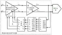
请参见图1,图1是本发明实施例提供的一种传感器模拟前端电路的流程示意图。本实施例提出了一种传感器模拟前端电路,该传感器模拟前端电路包括:增益自适应调节电路和缓冲电路,其中,增益自适应调节电路,连接信号输入端,用于对差分输入信号进行自适应增益调节,差分输入信号包括第一差分输入信号VIN、第二差分输入信号VIP;缓冲电路,连接增益自适应调节电路,用于对调节后的差分输入信号进行缓冲处理。本实施例通过增益自适应调节电路自动进行增益调节,使输出信号幅度稳定,然后缓冲电路输入阻抗高、输出阻抗低,可以完整传递增益自适应调节电路输出信号同时对输出信号进行隔离保护,完整输运信号,增强带负载的能力,增加延时,防止后级噪声对输出信号产生影响。Please refer to FIG. 1 . FIG. 1 is a schematic flowchart of a sensor analog front-end circuit provided by an embodiment of the present invention. This embodiment proposes a sensor analog front-end circuit, the sensor analog front-end circuit includes: a gain adaptive adjustment circuit and a buffer circuit, wherein the gain adaptive adjustment circuit is connected to the signal input end, and is used to adapt the differential input signal For gain adjustment, the differential input signal includes a first differential input signal VIN and a second differential input signal VIP ; a buffer circuit is connected to a gain adaptive adjustment circuit for buffering the adjusted differential input signal. In this embodiment, the gain adjustment is automatically performed by the gain adaptive adjustment circuit to stabilize the amplitude of the output signal, and then the buffer circuit has high input impedance and low output impedance, so that the output signal of the gain adaptive adjustment circuit can be completely transmitted and the output signal is isolated and protected. Transport signals, enhance the ability to carry loads, increase delays, and prevent post-stage noise from affecting output signals.
本实施例提出的传感器模拟前端电路,可以实现对输入信号的高精度获取与自适应增益调节,是一种高精度低功耗的传感器模拟前端电路。The sensor analog front-end circuit proposed in this embodiment can realize high-precision acquisition of input signals and adaptive gain adjustment, and is a sensor analog front-end circuit with high precision and low power consumption.
进一步地,本实施例增益自适应调节电路包括斩波调制可变增益放大电路、逐次逼近型模数转换器、二进制码转温度计码数字逻辑转换器、反相器。Further, the adaptive gain adjustment circuit of this embodiment includes a chopper modulation variable gain amplifier circuit, a successive approximation analog-to-digital converter, a binary code to thermometer code digital logic converter, and an inverter.
具体而言,请参见图2,图2是本发明实施例提供的传感器模拟前端电路中增益自适应调节电路的结构示意图,本实施例增益自适应调节中:斩波调制可变增益放大电路,连接信号输入端、缓冲电路,用于对差分输入信号进行自适应增益调节得到第一处理信号,第一处理信号包括第一差分输出信号VON、第二差分输出信号VOP,并将第一处理信号输出至缓冲电路,本实施例斩波调制可变增益放大电路在逐次逼近型模数转换器、二进制码转温度计码数字逻辑转换器和反相器控制环路的调控下,自动调节模拟前端电路差分输入信号,使输出的第一处理信号幅度稳定;逐次逼近型模数转换器,连接斩波调制可变增益放大电路,用于将第一处理信号量化为二进制码;二进制码转温度计码数字逻辑转换器,连接逐次逼近型模数转换器,用于将二进制码转化为温度计码;反相器,连接二进制码转温度计码数字逻辑转换器、斩波调制可变增益放大电路,用于将温度计码的高低电平进行翻转得到开关控制信号,并将开关控制信号输出至斩波调制可变增益放大电路,自动控制斩波调制可变增益放大电路的增益调节开关,进而完成对增益的自适应调节。其中,逐次逼近型模数转换器输出N位二进制码,并由二进制码转温度计码数字逻辑转换器将N位二进制码转为2N位温度计码,N为大于0的整数,比如二进制码000对应温度计码00000000,二进制码001对应温度计码00000001,二进制码010对应温度计码00000011,以此类推,二进制码111对应温度计码01111111。以N=6为例,请参见图3,图3是本发明实施例提供的传感器模拟前端电路中另一种增益自适应调节电路的结构示意图。Specifically, please refer to FIG. 2. FIG. 2 is a schematic structural diagram of the gain adaptive adjustment circuit in the sensor analog front-end circuit provided by the embodiment of the present invention. In the gain adaptive adjustment of this embodiment: the chopping modulation variable gain amplifier circuit, connected to the signal input terminal and the buffer circuit, for performing adaptive gain adjustment on the differential input signal to obtain the first processed signal, the first processed signal includes the first differential output signal VON , the second differential output signal VOP , and the first The processed signal is output to the buffer circuit. In this embodiment, the chopper modulation variable gain amplifier circuit automatically adjusts the analog signal under the control of the successive approximation analog-to-digital converter, the binary code to thermometer code digital logic converter and the inverter control loop. The differential input signal of the front-end circuit stabilizes the amplitude of the output first processed signal; the successive approximation analog-to-digital converter is connected to the chopper modulation variable gain amplifier circuit, which is used to quantize the first processed signal into binary code; the binary code is converted into a thermometer Code digital logic converter, connected with successive approximation analog-to-digital converter, used to convert binary code into thermometer code; inverter, connected with binary code to thermometer code digital logic converter, chopping modulation variable gain amplifier circuit, used Invert the high and low levels of the thermometer code to obtain the switch control signal, and output the switch control signal to the chopping modulation variable gain amplifier circuit, automatically control the gain adjustment switch of the chopping modulation variable gain amplifier circuit, and then complete the gain adjustment adaptive adjustment. Among them, the successive approximation analog-to-digital converter outputs N-bit binary code, and the binary code-to-thermometer code digital logic converter converts the N-bit binary code into 2N -bit thermometer code, and N is an integer greater than 0, such as binary code 000 Corresponds to thermometer code 00000000, binary code 001 corresponds to thermometer code 00000001, binary code 010 corresponds to thermometer code 00000011, and so on, binary code 111 corresponds to thermometer code 01111111. Taking N=6 as an example, please refer to FIG. 3 . FIG. 3 is a schematic structural diagram of another gain adaptive adjustment circuit in the sensor analog front-end circuit provided by an embodiment of the present invention.
进一步地,本实施例斩波调制可变增益放大电路包括第一斩波调制器CH1、第一偏置电路、第二偏置电路、第一开关电容阵列、第二开关电容阵列、第二斩波调制器CH2、全差分斩波调制放大电路OPA1、第一全差分放大器OPA2、第二全差分放大器OPA3、第一反馈电路、第二反馈电路。Further, the chopper modulation variable gain amplifier circuit in this embodiment includes a first chopper modulator CH1, a first bias circuit, a second bias circuit, a first switched capacitor array, a second switched capacitor array, a second chopper Wave modulator CH2, fully differential chopper modulation amplifier circuit OPA1, first fully differential amplifier OPA2, second fully differential amplifier OPA3, first feedback circuit, and second feedback circuit.
具体而言,请参见图4,图4是本发明实施例提供的增益自适应调节电路中斩波调制可变增益放大电路的结构示意图,本实施例斩波调制可变增益放大电路中:信号输入端与第一斩波调制器CH1连接,第一斩波调制器CH1的第一输出端、第一开关电容阵列、第一偏置电路、全差分斩波调制放大电路OPA1的正相输入端、第一全差分放大器OPA2的正相输入端、第二全差分放大器OPA3的正相输入端依次连接,第一斩波调制器CH1的第二输出端、第二开关电容阵列、第二偏置电路、全差分斩波调制放大电路OPA1的反相输入端、第一全差分放大器OPA2的反相输入端、第二全差分放大器OPA3的反相输入端依次连接,第一反馈电路跨接在全差分斩波调制放大器OPA1的正相输入端、第二全差分放大器OPA3的反相输出端之间,第二反馈电路跨接在全差分斩波调制放大电路OPA1的反相输入端、第二全差分放大器OPA3的正相输出端之间,第二全差分放大器OPA3的反相输出端与第一反馈电路之间、第二全差分放大器OPA3的正相输出端与第二反馈电路之间连接有第二斩波调制器CH2。其中,第一偏置电路包括一电阻RG1,电阻RG1的一端与全差分斩波调制放大电路OPA1的正相输入端连接,电阻RG1的另一端接VCM,第二偏置电路包括一电阻RG2,电阻RG2的一端与全差分斩波调制放大电路OPA1的反相输入端连接,电阻RG2的另一端接VCM;第一反馈电路包括一电容CS1,电容CS1的一端与全差分斩波调制放大电路OPA1的正相输入端连接,电容CS1的另一端与第二斩波调制器CH2的第一输出端连接,第二反馈电路包括一电容CS2,电容CS2的一端与全差分斩波调制放大电路OPA1的反相输入端连接,电容CS2的另一端与第二斩波调制器CH2的第二输出端连接。Specifically, please refer to FIG. 4. FIG. 4 is a schematic structural diagram of the chopping modulation variable gain amplifier circuit in the gain adaptive adjustment circuit provided by the embodiment of the present invention. In the chopping modulation variable gain amplifier circuit of this embodiment: the signal The input terminal is connected to the first chopping modulator CH1, the first output terminal of the first chopping modulator CH1, the first switched capacitor array, the first bias circuit, and the non-inverting input terminal of the fully differential chopping modulation amplifier circuit OPA1 , the positive phase input end of the first full differential amplifier OPA2, the positive phase input end of the second full differential amplifier OPA3 are connected sequentially, the second output end of the first chopper modulator CH1, the second switched capacitor array, the second bias circuit, the inverting input terminal of the fully differential chopper modulating amplifying circuit OPA1, the inverting input terminal of the first fully differential amplifier OPA2, and the inverting input terminal of the second fully differential amplifier OPA3 are connected sequentially, and the first feedback circuit is connected across the entire Between the non-inverting input terminal of the differential chopper modulating amplifier OPA1 and the inverting output terminal of the second fully differential amplifier OPA3, the second feedback circuit is connected across the inverting input terminal of the fully differential chopping modulating amplifying circuit OPA1, the second fully differential amplifier OPA3 Between the non-inverting output terminals of the differential amplifier OPA3, between the inverting output terminals of the second fully differential amplifier OPA3 and the first feedback circuit, and between the non-inverting output terminals of the second fully differential amplifier OPA3 and the second feedback circuit Second chopping modulator CH2. Wherein, the first bias circuit includes a resistor RG1 , one end of the resistor RG1 is connected to the non-inverting input end of the fully differential chopping modulation amplifier circuit OPA1, and the other end of the resistor RG1 is connected to VCM , and the second bias circuit includes A resistor RG2 , one end of the resistor RG2 is connected to the inverting input end of the fully differential chopping modulation amplifier circuit OPA1, and the other end of the resistor RG2 is connected to VCM ; the first feedback circuit includes a capacitor CS1 , the capacitor CS1 One end is connected to the non-inverting input end of the fully differential chopper modulation amplifier circuit OPA1, the other end of the capacitor CS1 is connected to the first output end of the second chopper modulator CH2, and the second feedback circuit includes a capacitor CS2 , the capacitor C S2 One end ofS2 is connected to the inverting input end of the fully differential chopping modulation amplifier circuit OPA1, and the other end of the capacitor CS2 is connected to the second output end of the second chopping modulator CH2.
本实施例斩波调制可变增益放大电路采用三级闭环全差分运放结构,包括全差分斩波调制放大器OPA1、第一全差分放大器OPA2、第二全差分放大器OPA3,全差分斩波调制放大电路OPA1为一全差分斩波调制折叠共源共栅放大器,第一全差分放大器OPA2、第二全差分放大器OPA3分别为一单级放大器,请参见图5,图5是本发明实施例提供的斩波调制可变增益放大电路中全差分斩波调制放大电路的结构示意图,图5为该全差分斩波调制折叠共源共栅放大器的具体电路结构,单级放大器电路结构具体不限。The chopper modulation variable gain amplifier circuit of this embodiment adopts a three-stage closed-loop fully differential operational amplifier structure, including a fully differential chopper modulation amplifier OPA1, a first fully differential amplifier OPA2, a second fully differential amplifier OPA3, and a fully differential chopper modulation amplifier. The circuit OPA1 is a fully differential chopping modulation folded cascode amplifier, the first fully differential amplifier OPA2 and the second fully differential amplifier OPA3 are respectively a single-stage amplifier, please refer to Figure 5, which is provided by the embodiment of the present invention The structural schematic diagram of the fully differential chopping modulation amplifier circuit in the chopping modulation variable gain amplifier circuit, Fig. 5 is the specific circuit structure of the fully differential chopping modulation folded cascode amplifier, the single stage amplifier circuit structure is not limited.
进一步地,请参见图6,图6是本发明实施例提供的增益自适应调节电路中另一种斩波调制可变增益放大电路的结构示意图,本实施例在上述图4的基础上,图4中第一开关电容阵列具体包括第一开关电容阵列包括2N组并联的第一电容开关电路,每组第一电容开关电路包括依次连接的一电容C、一开关Si,0≤i≤2N-1,每组第一电容开关电路中电容的另一端与第一斩波调制器CH1的第一输出端连接,每组第一电容开关电路中开关的另一端与第一偏置电路连接;图4中第二开关电容阵列具体包括第二开关电容阵列包括2N组并联的第二电容开关电路,每组第二电容开关电路包括依次连接的一电容C、一开关Si,每组第二电容开关电路中电容的另一端与第一斩波调制器CH1的第二输出端连接,每组第二电容开关电路中开关的另一端与第二偏置电路连接。本实施例以N=6为例,斩波调制可变增益放大电路在逐次逼近型模数转换器、二进制码转温度计码数字逻辑转换器和反相器的调节下,可以实现64级,单步长增益为1,总增益1~64的可调范围,自动调节斩波调制可变增益放大电路的输入信号,将输出信号固定在目标可处理信号范围内。Further, please refer to FIG. 6. FIG. 6 is a schematic structural diagram of another chopping modulation variable gain amplifier circuit in the gain adaptive adjustment circuit provided by the embodiment of the present invention. This embodiment is based on the above-mentioned FIG. 4, and the figure The first switched capacitor array in 4 specifically includes that the first switched capacitor array includes 2N groups of first capacitor switch circuits connected in parallel, and each group of first capacitor switch circuits includes a capacitor C and a switch Si connected in sequence, 0≤i≤ 2N -1, the other end of the capacitor in each group of the first capacitor switch circuit is connected to the first output end of the first chopper modulator CH1, and the other end of the switch in each group of the first capacitor switch circuit is connected to the first bias circuit Connection; the second switched capacitor array in Fig. 4 specifically includes the second switched capacitor array including 2N groups of second capacitor switch circuits connected in parallel, each group of second capacitor switch circuits includes a capacitor C and a switch Si connected in sequence, each The other end of the capacitor in the group of second capacitor switch circuits is connected to the second output end of the first chopper modulator CH1, and the other end of the switch in each group of second capacitor switch circuits is connected to the second bias circuit. In this embodiment, taking N=6 as an example, the chopper modulation variable gain amplifier circuit can realize 64 levels under the adjustment of the successive approximation analog-to-digital converter, binary code-to-thermometer code-digital logic converter, and inverter. The step gain is 1, and the total gain is adjustable from 1 to 64. The input signal of the chopper modulation variable gain amplifier circuit is automatically adjusted, and the output signal is fixed within the target signal range that can be processed.
进一步地,本实施例逐次逼近型模数转换器包括自举开关、第三电容阵列、动态比较器和SAR控制逻辑器。Further, the successive approximation analog-to-digital converter in this embodiment includes a bootstrap switch, a third capacitor array, a dynamic comparator, and a SAR control logic.
具体而言,请参见图7,图7是本发明实施例提供的增益自适应调节电路中逐次逼近型模数转换器的结构示意图,本实施例逐次逼近型模数转换器中:自举开关,连接斩波调制可变增益放大电路,用于对第一处理信号进行采样得到采样信号,实现高质量采样;第三电容阵列,连接自举开关,用于根据开关控制信号对采样信号进行更新,优选地,第三电容阵列为差分等比例电容阵列;动态比较器,连接第三电容阵列,用于比较参考信号Vref、更新的采样信号得到比较结果;SAR控制逻辑器,连接动态比较器、第三电容阵列、二进制码转温度计码数字逻辑转换器,用于根据比较结果量化输出二进制码,将二进制码输入至二进制码转温度计码数字逻辑转换器,并更新开关控制信号,将更新的开关控制信号输入至第三电容阵列,SAR控制逻辑器在锁存本周期比较结果的同时控制下一周期第三电容阵列的打开/关闭操作。Specifically, please refer to FIG. 7. FIG. 7 is a schematic structural diagram of the successive approximation analog-to-digital converter in the gain adaptive adjustment circuit provided by the embodiment of the present invention. In the successive approximation analog-to-digital converter of this embodiment: the bootstrap switch , connected to the chopper modulation variable gain amplifier circuit, used to sample the first processed signal to obtain a sampled signal to achieve high-quality sampling; the third capacitor array, connected to the bootstrap switch, used to update the sampled signal according to the switch control signal , preferably, the third capacitor array is a differential equal-proportion capacitor array; the dynamic comparator is connected to the third capacitor array, and is used to compare the reference signal Vref and the updated sampling signal to obtain a comparison result; the SAR control logic is connected to the dynamic comparator , a third capacitor array, and a binary code-to-thermometer code digital logic converter, used to quantify and output binary codes according to the comparison result, input the binary codes to the binary code-to-thermometer code digital logic converter, and update the switch control signal, and update the updated The switch control signal is input to the third capacitor array, and the SAR control logic controls the on/off operation of the third capacitor array in the next cycle while latching the comparison result of the current cycle.
进一步地,本实施例增益自适应调节电路还包括单位增益放大电路。Further, the gain adaptive adjustment circuit in this embodiment further includes a unity gain amplifier circuit.
具体而言,请参见图8,图8是本发明实施例提供的传感器模拟前端电路中再一种增益自适应调节电路的结构示意图,本实施例在图2基础上,增益自适应调节电路还包括单位增益放大电路,整个电路结构中:斩波调制可变增益放大电路,用于对差分输入信号进行自适应增益调节得到第一处理信号;单位增益放大电路,连接斩波调制可变增益放大电路、缓冲电路,用于对第一处理信号进行单位增益放大得到第二处理信号,第二处理信号包括第三差分输出信号VON1、第四差分输出信号VOP1,并将第二处理信号输出至缓冲电路;逐次逼近型模数转换器,连接单位增益放大电路,用于将第二处理信号量化为二进制码;二进制码转温度计码数字逻辑转换器,连接逐次逼近型模数转换器,用于将二进制码转化为温度计码;反相器,连接二进制码转温度计码数字逻辑转换器、斩波调制可变增益放大电路,用于将温度计码的高低电平进行翻转得到开关控制信号,并将开关控制信号输出至斩波调制可变增益放大电路。具体图8所示的增益自适应调节电路实现原理类似图2所示的增益自适应调节电路,唯一不同的是增加了单位增益放大电路,对斩波调制可变增益放大电路输出信号进行1倍增益放大,将斩波调制可变增益放大电路输出信号进行完整输运,提供低输出阻抗,将斩波调制可变增益放大电路输出信号进行单位增益放大后输出至缓冲电路、逐次逼近型模数转换器。对应地,以N=6为例,请参见图9,图9是本发明实施例提供的传感器模拟前端电路中又一种增益自适应调节电路的结构示意。Specifically, please refer to FIG. 8. FIG. 8 is a schematic structural diagram of another gain adaptive adjustment circuit in the sensor analog front-end circuit provided by the embodiment of the present invention. On the basis of FIG. 2 in this embodiment, the gain adaptive adjustment circuit is also Including the unit gain amplifier circuit, in the whole circuit structure: the chopper modulation variable gain amplifier circuit is used to perform adaptive gain adjustment on the differential input signal to obtain the first processed signal; the unit gain amplifier circuit is connected to the chopping modulation variable gain amplifier circuit The circuit and the buffer circuit are used to amplify the first processing signal with unity gain to obtain the second processing signal, the second processing signal includes the third differential output signal VON1 and the fourth differential output signal VOP1 , and output the second processing signal to the buffer circuit; the successive approximation analog-to-digital converter is connected to the unit gain amplifier circuit, and is used to quantize the second processed signal into binary code; the binary code to thermometer code digital logic converter is connected to the successive approximation analog-to-digital converter, using It is used to convert the binary code into a thermometer code; the inverter is connected to a binary code-to-thermometer code digital logic converter and a chopper modulation variable gain amplifier circuit, which is used to reverse the high and low levels of the thermometer code to obtain a switch control signal, and The switch control signal is output to the chopper modulation variable gain amplifier circuit. Specifically, the realization principle of the gain adaptive adjustment circuit shown in Figure 8 is similar to the gain adaptive adjustment circuit shown in Figure 2, the only difference is that a unit gain amplifier circuit is added, and the output signal of the chopper modulation variable gain amplifier circuit is doubled. Gain amplification, the output signal of the chopping modulation variable gain amplifier circuit is completely transported, and low output impedance is provided, the output signal of the chopping modulation variable gain amplifier circuit is amplified by unity gain and then output to the buffer circuit, successive approximation modulus converter. Correspondingly, taking N=6 as an example, please refer to FIG. 9 , which is a schematic structural diagram of another gain adaptive adjustment circuit in the sensor analog front-end circuit provided by an embodiment of the present invention.
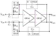
请参见图10,图10是本发明实施例提供的增益自适应调节电路中单位增益放大电路的结构示意图,本实施例单位增益放大电路包括电容C1、电容C2、第一偏置电路、第二偏置电路、第三全差分放大器OPA4、第四全差分放大器OPA5、第一反馈电路、第二反馈电路,电容C1、第一偏置电路、第三全差分放大器OPA4的正相输入端、第四全差分放大器OPA5的正相输入端连接,电容C2、第二偏置电路、第三全差分放大器OPA4的反相输入端、第四全差分放大器OPA5的反相输入端连接,第三全差分放大器OPA4的正相输入端与第四全差分放大器OPA5的正相输出端之间跨接第一反馈电路,第三全差分放大器OPA4的反相输入端与第四全差分放大器OPA5的反相输出端之间跨接第二反馈电路。其中,第一偏置电路、第二偏置电路、第一反馈电路、第二反馈电路采用与图6所示斩波调制可变增益放大电路中第一偏置电路、第二偏置电路、第一反馈电路、第二反馈电路相同的电路结构,在此不再赘述。Please refer to FIG. 10. FIG. 10 is a schematic structural diagram of a unity gain amplifier circuit in a gain adaptive adjustment circuit provided by an embodiment of the present invention. The unity gain amplifier circuit of this embodiment includes a capacitor C1 , a capacitor C2 , a first bias circuit, The second bias circuit, the third fully differential amplifier OPA4, the fourth fully differential amplifier OPA5, the first feedback circuit, the second feedback circuit, the capacitor C1 , the first bias circuit, the positive phase input of the third fully differential amplifier OPA4 terminal, the noninverting input terminal of the fourth fully differential amplifier OPA5, the capacitorC2 , the second bias circuit, the inverting input terminal of the third fully differential amplifier OPA4, and the inverting input terminal of the fourth fully differential amplifier OPA5, The first feedback circuit is connected between the non-inverting input terminal of the third fully differential amplifier OPA4 and the non-inverting output terminal of the fourth fully differential amplifier OPA5, and the inverting input terminal of the third fully differential amplifier OPA4 is connected to the fourth fully differential amplifier OPA5. The second feedback circuit is connected across the inverting output terminals of the two. Wherein, the first bias circuit, the second bias circuit, the first feedback circuit, and the second feedback circuit adopt the first bias circuit, the second bias circuit, the second bias circuit, The circuit structures of the first feedback circuit and the second feedback circuit are the same, and will not be repeated here.
本实施例单位增益放大电路采用两级闭环全差分运放结构,包括第三全差分放大器OPA4、第四全差分放大器OPA5,第三全差分放大器OPA4、第四全差分放大器OPA5均为一单级放大器,可以采用与第一全差分放大器OPA2、第二全差分放大器OPA3相同的单级放大器电路结构,单级放大器电路结构具体不限。The unit gain amplifier circuit of this embodiment adopts a two-stage closed-loop fully differential operational amplifier structure, including the third fully differential amplifier OPA4, the fourth fully differential amplifier OPA5, the third fully differential amplifier OPA4, and the fourth fully differential amplifier OPA5 are all single-stage The amplifier may adopt the same single-stage amplifier circuit structure as the first fully differential amplifier OPA2 and the second fully differential amplifier OPA3, and the single-stage amplifier circuit structure is not specifically limited.
进一步地,请参见图11,图11是本发明实施例提供的增益自适应调节电路中另一种逐次逼近型模数转换器的结构示意图,本实施例增加了单位增益放大电路的增益自适应调节电路中,逐次逼近型模数转换器不再连接斩波调制可变增益放大电路,而是连接单位增益放大电路,单位增益放大电路输出的第二处理信号输入至逐次逼近型模数转换器,具体:自举开关,连接单位增益放大电路,用于对第二处理信号进行采样得到采样信号;第三电容阵列,连接自举开关,用于根据开关控制信号对采样信号进行更新;动态比较器,连接第三电容阵列,用于比较参考信号、更新的采样信号得到比较结果;SAR控制逻辑器,连接动态比较器、第三电容阵列、二进制码转温度计码数字逻辑转换器,用于根据比较结果量化输出二进制码,将二进制码输入至二进制码转温度计码数字逻辑转换器,并更新开关控制信号,将更新的开关控制信号输入至第三电容阵列。Further, please refer to FIG. 11. FIG. 11 is a schematic structural diagram of another successive approximation analog-to-digital converter in the gain adaptive adjustment circuit provided by the embodiment of the present invention. In this embodiment, the gain adaptive gain of the unity gain amplifier circuit is added. In the adjustment circuit, the successive approximation analog-to-digital converter is no longer connected to the chopping modulation variable gain amplifier circuit, but is connected to the unit gain amplifier circuit, and the second processed signal output by the unit gain amplifier circuit is input to the successive approximation analog-to-digital converter , specifically: a bootstrap switch, connected to a unity gain amplifier circuit, used to sample the second processed signal to obtain a sampling signal; the third capacitor array, connected to a bootstrap switch, used to update the sampled signal according to the switch control signal; dynamic comparison The device is connected to the third capacitor array, which is used to compare the reference signal and the updated sampling signal to obtain the comparison result; the SAR control logic device is connected to the dynamic comparator, the third capacitor array, and the binary code to thermometer code digital logic converter, which is used to obtain the comparison result according to the The comparison result is quantized to output a binary code, and the binary code is input to a binary code-to-thermometer code digital logic converter, and a switch control signal is updated, and the updated switch control signal is input to the third capacitor array.
本实施例提供的传感器模拟前端电路中,斩波调制可变增益放大电路首先对差分输入信号进行斩波调制,将差分输入信号输入至斩波调制可变增益放大电路的差分输入端,以初始默认增益对差分输入信号放大并有斩波开关模块解调;单位增益放大电路将斩波调制可变增益放大电路的输出信号放大单位增益;6位逐次逼近型模数转换器将单位增益放大电路的输出信号量化为6位二进制码A5~A0;二进制码转温度计码数字逻辑转换器将6位二进制码A5~A0转换为64位温度计码T63~T0,64位温度计码输出接反相器后,反馈接回至斩波调制可变增益放大电路,并控制斩波调制可变增益放大电路增益的开关,每一位温度计码输出经反相器进行高低电平翻转后对应斩波调制可变增益放大电路中一个开关,T0温度计码输出接反相器后输出TN0,反馈至开关S0,T1温度计码输出接反相器后输出TN1,反馈至开关S1,T2温度计码输出接反相器后输出TN2,反馈至开关S2,以此类推,T62温度计码输出接反相器后输出TN62,反馈至开关S62,T63温度计码输出接反相器后输出TN63,反馈至开关S63,具体调节机理举例如下:In the sensor analog front-end circuit provided in this embodiment, the chopping modulation variable gain amplifier circuit first performs chopping modulation on the differential input signal, and then inputs the differential input signal to the differential input terminal of the chopping modulation variable gain amplifier circuit to initially The default gain amplifies the differential input signal and demodulates it with a chopper switch module; the unit gain amplifier circuit amplifies the output signal of the chopper modulation variable gain amplifier circuit to unity gain; the 6-bit successive approximation analog-to-digital converter converts the unit gain amplifier circuit to The output signal is quantized into 6-bit binary code A5 ~A0 ; binary code to thermometer code digital logic converter converts 6-bit binary code A5 ~A0 into 64-bit thermometer code T63 ~T0 , 64-bit thermometer code After the output is connected to the inverter, the feedback is connected to the chopping modulation variable gain amplifier circuit, and the switch of the gain of the chopping modulation variable gain amplifier circuit is controlled. The output of each thermometer code is flipped from high to low by the inverter. Corresponding to a switch in the chopping modulation variable gain amplifier circuit, the T0 thermometer code output is connected to the inverter and then outputs TN0 , which is fed back to the switch S0 , and the T1 thermometer code output is connected to the inverter and outputs TN1 , which is fed back to the switch S1 , T2 thermometer code output connected to the inverter and output TN2 , fed back to switch S2 , and so on, T62 thermometer code output connected to the inverter and output TN62 , fed back to switch S62 , T63 thermometer After the code output is connected to the inverter, it outputs TN63 , which is fed back to the switch S63 . The specific adjustment mechanism is as follows:
(1)、当差分输入信号较大时,经斩波调制可变增益放大电路和单位增益放大电路增益放大后,输入逐次逼近型模数转换器,量化输出二进制码,此时假设输出二进制码A5~A0=1,二进制码转温度计码数字逻辑转换器将二进制码A5~A0=1转化为温度计码:T63=0,T62~T0=1,反相器将温度计码输出对应转换为TN63=1,TN62~TN0=0,反馈至斩波调制可变增益放大电路增益控制开关,TN63对应开关S63,TN62对应开关S62,以此类推,TN61~TN0分别对应开关S61~S0,此时第一开关电容阵列、第二开关电容阵列中电容C只有1路导通,增益为C/C=1,降低增益,完成一次对信号增益放大的自动调节,下一周期继续重复上述操作,直至模拟前端电路输出的模拟信号满足固定信号幅度范围,缓冲电路将自动调节后的模拟输出信号进行单位增益放大,输出至模数转换电路处理。(1) When the differential input signal is large, after the chopping modulates the variable gain amplifier circuit and the unit gain amplifier circuit gain amplification, it is input to the successive approximation analog-to-digital converter, and the binary code is quantized and output. At this time, it is assumed that the binary code is output A5 ~ A0 = 1, binary code to thermometer code digital logic converter converts binary code A5 ~ A0 = 1 into thermometer code: T63 = 0, T62 ~ T0 = 1, inverter converts thermometer code The corresponding output is converted to TN63 = 1, TN62 ~ TN0 = 0, fed back to the gain control switch of the chopper modulation variable gain amplifier circuit, TN63 corresponds to the switch S63 , TN62 corresponds to the switch S62 , and so on, TN61 ~ TN0 correspond to switches S61 ~ S0 respectively. At this time, only one path of capacitor C in the first switched capacitor array and the second switched capacitor array is turned on, and the gain is C/C=1. Reduce the gain to complete a signal pairing Automatic adjustment of gain amplification, repeat the above operation in the next cycle, until the analog signal output by the analog front-end circuit meets the fixed signal amplitude range, the buffer circuit will perform unity gain amplification on the automatically adjusted analog output signal, and output it to the analog-to-digital conversion circuit for processing .
(2)、当差分输入信号较小时,经由斩波调制可变增益放大电路和单位增益放大电路增益放大后,输入至逐次逼近型模数转换器,量化输出二进制码,此时假设输出二进制码A5~A1=0、A0=1,二进制码转温度计码数字逻辑转换器将二进制码A5~A1=0、A0=1转化为温度计码:T63~T1=0,T0=1,反相器将温度计码输出对应转换为TN63~TN1=1,TN0=0,反馈至斩波调制可变增益放大电路增益控制开关,TN63对应开关S63,TN62对应开关S62,以此类推,TN61~TN0分别对应开关S61~S0,此时第一开关电容阵列、第二开关电容阵列中电容C有63路导通,增益为63C/C=63,提升了增益,完成一次对信号增益放大的自动调节,下一周期继续重复上述操作,直至模拟前端输出的模拟信号满足固定信号幅度范围。缓冲电路将自动调节后的模拟输出信号进行单位增益放大,输出至模数转换电路处理。(2) When the differential input signal is small, after the gain is amplified by the chopper modulation variable gain amplifier circuit and the unity gain amplifier circuit, it is input to the successive approximation analog-to-digital converter, and the binary code is quantized and output. At this time, it is assumed that the binary code is output A5 ~A1 =0, A0 =1, binary code to thermometer code digital logic converter converts binary code A5 ~A1 =0, A0 =1 into thermometer code: T63 ~T1 =0, T0 =1, the inverter converts the thermometer code output correspondingly to TN63 ~ TN1 =1, TN0 =0, feeds back to the gain control switch of the chopper modulation variable gain amplifier circuit, TN63 corresponds to the switch S63 , TN62 corresponds to the switch S62 , and so on, TN61 ~ TN0 respectively correspond to the switches S61 ~ S0 , at this time, there are 63 circuits of capacitor C in the first switched capacitor array and the second switched capacitor array, and the gain is 63C/ C=63, the gain is increased, and an automatic adjustment of the signal gain amplification is completed, and the above operation is repeated in the next cycle until the analog signal output by the analog front end meets the fixed signal amplitude range. The buffer circuit amplifies the automatically adjusted analog output signal with unity gain, and outputs it to the analog-to-digital conversion circuit for processing.
本实施例缓冲电路可以采用与单位增益放大电路类似的两级闭环全差分运放结构,闭环增益设定为1。The buffer circuit of this embodiment may adopt a two-stage closed-loop fully differential operational amplifier structure similar to the unity gain amplifier circuit, and the closed-loop gain is set to 1.
综上所述,本实施例提出的传感器模拟前端电路,采用斩波调制技术和自适应增益调节技术,将斩波调制可变增益放大电路、低功耗逐次逼近型模数转换器、二进制码转温度计码数字逻辑转换器、缓冲电路单芯片全集成的方式,并由斩波调制可变增益放大电路、低功耗逐次逼近型模数转换器、二进制码转温度计码数字逻辑转换器、反相器完成闭环增益自适应调节,具有精度高、可配置性强的优势,同时辅助电路采用逐次逼近型模数转换器,实现了超低功耗反馈调节,降低了整体电路功耗,适用于便携式可穿戴医疗设备中。To sum up, the sensor analog front-end circuit proposed in this embodiment adopts chopping modulation technology and adaptive gain adjustment technology to combine chopping modulation variable gain amplifier circuit, low power successive approximation analog-to-digital converter, binary code Convert thermometer code digital logic converter, buffer circuit single chip fully integrated way, and by chopper modulation variable gain amplifier circuit, low power consumption successive approximation analog-to-digital converter, binary code to thermometer code digital logic converter, inverse The phase device completes the closed-loop gain adaptive adjustment, which has the advantages of high precision and strong configurability. At the same time, the auxiliary circuit adopts a successive approximation analog-to-digital converter, which realizes ultra-low power consumption feedback adjustment and reduces the overall circuit power consumption. It is suitable for in portable wearable medical devices.
以上内容是结合具体的优选实施方式对本发明所作的进一步详细说明,不能认定本发明的具体实施只局限于这些说明。对于本发明所属技术领域的普通技术人员来说,在不脱离本发明构思的前提下,还可以做出若干简单推演或替换,都应当视为属于本发明的保护范围。The above content is a further detailed description of the present invention in conjunction with specific preferred embodiments, and it cannot be assumed that the specific implementation of the present invention is limited to these descriptions. For those of ordinary skill in the technical field of the present invention, without departing from the concept of the present invention, some simple deduction or replacement can be made, which should be regarded as belonging to the protection scope of the present invention.
Claims (1)
Translated fromChinesePriority Applications (1)
| Application Number | Priority Date | Filing Date | Title |
|---|---|---|---|
| CN202110383612.3ACN113285718B (en) | 2021-04-09 | 2021-04-09 | Sensor analog front-end circuit |
Applications Claiming Priority (1)
| Application Number | Priority Date | Filing Date | Title |
|---|---|---|---|
| CN202110383612.3ACN113285718B (en) | 2021-04-09 | 2021-04-09 | Sensor analog front-end circuit |
Publications (2)
| Publication Number | Publication Date |
|---|---|
| CN113285718A CN113285718A (en) | 2021-08-20 |
| CN113285718Btrue CN113285718B (en) | 2023-04-07 |
Family
ID=77276350
Family Applications (1)
| Application Number | Title | Priority Date | Filing Date |
|---|---|---|---|
| CN202110383612.3AActiveCN113285718B (en) | 2021-04-09 | 2021-04-09 | Sensor analog front-end circuit |
Country Status (1)
| Country | Link |
|---|---|
| CN (1) | CN113285718B (en) |
Families Citing this family (1)
| Publication number | Priority date | Publication date | Assignee | Title |
|---|---|---|---|---|
| CN115459714A (en)* | 2022-09-02 | 2022-12-09 | 上海交通大学 | Signal folding amplifier based on capacitive digital-to-analog converter and signal chain circuit thereof |
Citations (5)
| Publication number | Priority date | Publication date | Assignee | Title |
|---|---|---|---|---|
| US6823028B1 (en)* | 2000-05-12 | 2004-11-23 | National Semiconductor Corporation | Digitally controlled automatic gain control system for use in an analog front-end of a receiver |
| CN201672968U (en)* | 2010-05-14 | 2010-12-15 | 成都赛腾自动化工程有限公司 | Adaptive signal adjusting device for vibrating sensor |
| WO2015154671A1 (en)* | 2014-04-09 | 2015-10-15 | 华为技术有限公司 | Self-calibration method and device for pipeline successive approximation type analogue to digital convertor |
| KR101923829B1 (en)* | 2017-10-26 | 2018-11-29 | 서울대학교산학협력단 | Semiconductor device for reading out signal from sensor |
| CN111803069A (en)* | 2020-08-11 | 2020-10-23 | 江苏德长医疗科技有限公司 | Self-adaptive dynamic gain adjustment pressure distribution measuring system |
Family Cites Families (2)
| Publication number | Priority date | Publication date | Assignee | Title |
|---|---|---|---|---|
| TW481390U (en)* | 2000-12-15 | 2002-03-21 | Ind Tech Res Inst | Automatic gain adjusting circuit for analog signal |
| TWI692112B (en)* | 2019-03-11 | 2020-04-21 | 茂達電子股份有限公司 | Light sensor having adaptively controlled gain |
- 2021
- 2021-04-09CNCN202110383612.3Apatent/CN113285718B/enactiveActive
Patent Citations (5)
| Publication number | Priority date | Publication date | Assignee | Title |
|---|---|---|---|---|
| US6823028B1 (en)* | 2000-05-12 | 2004-11-23 | National Semiconductor Corporation | Digitally controlled automatic gain control system for use in an analog front-end of a receiver |
| CN201672968U (en)* | 2010-05-14 | 2010-12-15 | 成都赛腾自动化工程有限公司 | Adaptive signal adjusting device for vibrating sensor |
| WO2015154671A1 (en)* | 2014-04-09 | 2015-10-15 | 华为技术有限公司 | Self-calibration method and device for pipeline successive approximation type analogue to digital convertor |
| KR101923829B1 (en)* | 2017-10-26 | 2018-11-29 | 서울대학교산학협력단 | Semiconductor device for reading out signal from sensor |
| CN111803069A (en)* | 2020-08-11 | 2020-10-23 | 江苏德长医疗科技有限公司 | Self-adaptive dynamic gain adjustment pressure distribution measuring system |
Non-Patent Citations (2)
| Title |
|---|
| "Design of AGC amplifier for CMOS Image Sensor";Guoyi Yu等;《2012 IEEE International Symposium on Radio-Frequency Integration Technology (RFIT)》;20130107;第34-36页* |
| "低压低功耗智能传感器模拟前端设计进展";陈铖颖等;《微电子学》;20150228;第45卷(第1期);第88-93页* |
Also Published As
| Publication number | Publication date |
|---|---|
| CN113285718A (en) | 2021-08-20 |
Similar Documents
| Publication | Publication Date | Title |
|---|---|---|
| CN111277236B (en) | A kind of front-end circuit and dynamic range improvement method based on gain adaptive adjustment | |
| Li et al. | An ECG recording front-end with continuous-time level-crossing sampling | |
| CN110311677B (en) | SAR ADC based on novel capacitance switch switching algorithm | |
| JP2779267B2 (en) | Preamplifier circuit | |
| TWI459723B (en) | Zero-crossing-based analog/digital convertor with current mismatch correction | |
| CN111294051B (en) | Automatic gain adjustment amplifying circuit based on successive approximation type analog-to-digital converter | |
| Yazdani et al. | A low power fully differential level-crossing ADC with low power charge redistribution input for biomedical applications | |
| CN113285718B (en) | Sensor analog front-end circuit | |
| WO2024119815A1 (en) | Two-stage successive-approximation-register analog-to-digital converter based on differential amplifier | |
| CN102723951A (en) | Pipelined ADC (Analog-to-Digital Converter) digital background correcting circuit with translation technology | |
| CN110224701B (en) | Pipelined ADC | |
| CN119315988B (en) | Analog-to-digital converter, conversion method and electronic product | |
| TWI782692B (en) | Multiplying digital-to-analog converter with pre-sampling and associated pipelined analog-to-digital converter | |
| CN109302185A (en) | A cyclic analog-to-digital converter with multiplexing operational amplifier and its conversion method | |
| CN110120814B (en) | A current comparator and comparison method for eliminating offset error | |
| CN114696829A (en) | Analog-to-digital conversion circuit and pipeline analog-to-digital converter | |
| CN118138050A (en) | A direct quantization analog front-end interface circuit based on delta modulator | |
| Zhu et al. | A 1.8 V, SNDR 96.3 dB analog front-end circuit design for ECG signal acquisition | |
| Trivedi | Low power and high speed sample-and-hold circuit | |
| AU2015349443A1 (en) | DC offset cancellation method and device | |
| Adimulam et al. | A low power, low noise Programmable Analog Front End (PAFE) for biopotential measurements | |
| Fujimoto et al. | A switched-capacitor variable gain amplifier for CCD image sensor interface system | |
| US20100141492A1 (en) | Low power consumption analog-to-digital converter | |
| El-Sankary et al. | Low power, low voltage, 10bit-50MSPS pipeline ADC dedicated for front-end ultrasonic receivers | |
| US20200358400A1 (en) | High signal-to-noise ratio amplifier with multiple output modes |
Legal Events
| Date | Code | Title | Description |
|---|---|---|---|
| PB01 | Publication | ||
| PB01 | Publication | ||
| SE01 | Entry into force of request for substantive examination | ||
| SE01 | Entry into force of request for substantive examination | ||
| GR01 | Patent grant | ||
| GR01 | Patent grant |