CN113285197B - Three-dimensional impedance network double-side loaded slow wave substrate integrated waveguide and design method thereof - Google Patents
Three-dimensional impedance network double-side loaded slow wave substrate integrated waveguide and design method thereofDownload PDFInfo
- Publication number
- CN113285197B CN113285197BCN202110553726.8ACN202110553726ACN113285197BCN 113285197 BCN113285197 BCN 113285197BCN 202110553726 ACN202110553726 ACN 202110553726ACN 113285197 BCN113285197 BCN 113285197B
- Authority
- CN
- China
- Prior art keywords
- impedance network
- integrated waveguide
- substrate
- substrate integrated
- slow wave
- Prior art date
- Legal status (The legal status is an assumption and is not a legal conclusion. Google has not performed a legal analysis and makes no representation as to the accuracy of the status listed.)
- Active
Links
- 239000000758substrateSubstances0.000titleclaimsabstractdescription89
- 238000013461designMethods0.000titleclaimsdescription15
- 238000000034methodMethods0.000titleclaimsdescription11
- 239000002184metalSubstances0.000claimsabstractdescription83
- 229910052751metalInorganic materials0.000claimsabstractdescription83
- 238000000576coating methodMethods0.000claimsabstractdescription40
- 239000011248coating agentSubstances0.000claimsabstractdescription35
- 238000003491arrayMethods0.000claimsabstractdescription5
- WYTGDNHDOZPMIW-RCBQFDQVSA-NalstonineNatural productsC1=CC2=C3C=CC=CC3=NC2=C2N1C[C@H]1[C@H](C)OC=C(C(=O)OC)[C@H]1C2WYTGDNHDOZPMIW-RCBQFDQVSA-N0.000claimsdescription37
- 230000007704transitionEffects0.000claimsdescription15
- RYGMFSIKBFXOCR-UHFFFAOYSA-NCopperChemical compound[Cu]RYGMFSIKBFXOCR-UHFFFAOYSA-N0.000claimsdescription12
- 229910052802copperInorganic materials0.000claimsdescription12
- 239000010949copperSubstances0.000claimsdescription12
- 238000001465metallisationMethods0.000claimsdescription10
- 239000003989dielectric materialSubstances0.000claimsdescription4
- 239000007787solidSubstances0.000claims1
- 230000000694effectsEffects0.000abstractdescription23
- 230000005684electric fieldEffects0.000abstractdescription9
- 238000000926separation methodMethods0.000abstractdescription5
- 230000002457bidirectional effectEffects0.000abstractdescription4
- 239000011247coating layerSubstances0.000description13
- 239000010410layerSubstances0.000description11
- 238000011068loading methodMethods0.000description10
- 238000010586diagramMethods0.000description9
- 230000005540biological transmissionEffects0.000description8
- 230000003071parasitic effectEffects0.000description6
- 238000012545processingMethods0.000description4
- 239000012141concentrateSubstances0.000description3
- 238000004519manufacturing processMethods0.000description3
- 230000008569processEffects0.000description3
- 230000002708enhancing effectEffects0.000description2
- 238000003780insertionMethods0.000description2
- 230000037431insertionEffects0.000description2
- 239000000463materialSubstances0.000description2
- 238000012986modificationMethods0.000description2
- 230000004048modificationEffects0.000description2
- 238000011160researchMethods0.000description2
- 238000004088simulationMethods0.000description2
- 241000270295SerpentesSpecies0.000description1
- 230000009286beneficial effectEffects0.000description1
- 239000003990capacitorSubstances0.000description1
- 238000005253claddingMethods0.000description1
- 230000007547defectEffects0.000description1
- 238000011161developmentMethods0.000description1
- 238000009826distributionMethods0.000description1
- 230000006872improvementEffects0.000description1
- 230000010354integrationEffects0.000description1
- 239000002356single layerSubstances0.000description1
- 238000003466weldingMethods0.000description1
Images


Classifications
- H—ELECTRICITY
- H01—ELECTRIC ELEMENTS
- H01P—WAVEGUIDES; RESONATORS, LINES, OR OTHER DEVICES OF THE WAVEGUIDE TYPE
- H01P3/00—Waveguides; Transmission lines of the waveguide type
- H01P3/16—Dielectric waveguides, i.e. without a longitudinal conductor
- H—ELECTRICITY
- H01—ELECTRIC ELEMENTS
- H01P—WAVEGUIDES; RESONATORS, LINES, OR OTHER DEVICES OF THE WAVEGUIDE TYPE
- H01P11/00—Apparatus or processes specially adapted for manufacturing waveguides or resonators, lines, or other devices of the waveguide type
- H01P11/001—Manufacturing waveguides or transmission lines of the waveguide type
- H01P11/003—Manufacturing lines with conductors on a substrate, e.g. strip lines, slot lines
- H—ELECTRICITY
- H01—ELECTRIC ELEMENTS
- H01P—WAVEGUIDES; RESONATORS, LINES, OR OTHER DEVICES OF THE WAVEGUIDE TYPE
- H01P11/00—Apparatus or processes specially adapted for manufacturing waveguides or resonators, lines, or other devices of the waveguide type
- H01P11/001—Manufacturing waveguides or transmission lines of the waveguide type
- H01P11/006—Manufacturing dielectric waveguides
- H—ELECTRICITY
- H01—ELECTRIC ELEMENTS
- H01P—WAVEGUIDES; RESONATORS, LINES, OR OTHER DEVICES OF THE WAVEGUIDE TYPE
- H01P3/00—Waveguides; Transmission lines of the waveguide type
- H01P3/02—Waveguides; Transmission lines of the waveguide type with two longitudinal conductors
- H01P3/08—Microstrips; Strip lines
- H01P3/081—Microstriplines
Landscapes
- Engineering & Computer Science (AREA)
- Manufacturing & Machinery (AREA)
- Waveguides (AREA)
Abstract
Description
Translated fromChinese技术领域technical field
本发明涉及微波无源器件技术领域,具体而言,涉及三维阻抗网络双面加载的慢波基片集成波导及其设计方法。The invention relates to the technical field of microwave passive devices, in particular to a slow-wave substrate integrated waveguide loaded on both sides of a three-dimensional impedance network and a design method thereof.
背景技术Background technique
基片集成波导(Substrate Integrated Waveguide, SIW)技术作为一种新型导波结构,它既保持了传统金属波导的高Q值、低损耗、高功率容量等优点,又易于与微带线、共面波导等各种平面结构相集成。随着印刷电路板等电路加工工艺的发展,SIW剖面低、尺寸小、易加工等传统矩形金属波导不具备的优势更加凸显。因此,SIW已广泛地运用于微波毫米波电路系统及微波元器件的设计,如滤波器、定向耦合器、移相器、功率分配/合成器等。Substrate Integrated Waveguide (SIW) technology, as a new type of guided wave structure, not only maintains the advantages of high Q value, low loss, and high power capacity of traditional metal waveguides, but also is easy to integrate with microstrip lines, coplanar Various planar structures such as waveguides are integrated. With the development of circuit processing technology such as printed circuit boards, the advantages of SIW, which are not available in traditional rectangular metal waveguides, such as low profile, small size, and easy processing, are more prominent. Therefore, SIW has been widely used in the design of microwave and millimeter-wave circuit systems and microwave components, such as filters, directional couplers, phase shifters, power distribution/combiners, etc.
对于微波低频段的应用来说,由于SIW 固有截止频率的限制,其占电路面积仍然过大,这制约着其在紧凑型微波系统中的应用。2014年,法国格勒诺布尔大学A. Niembro-Martín等人首次提出慢波基片集成波导(Slow-Wave Substrate Integrated Waveguide,SW-SIW)的概念,寄托于各类加载手段提升基片材料的等效电磁参数,突破导波传播的限制,以获得慢波效应。对于SIW小型化技术来说,具有十分重要的工程意义和科研价值。For the application of microwave low frequency band, due to the limitation of the inherent cutoff frequency of SIW, its circuit area is still too large, which restricts its application in compact microwave systems. In 2014, A. Niembro-Martín and others from the University of Grenoble in France first proposed the concept of Slow-Wave Substrate Integrated Waveguide (SW-SIW), which relies on various loading methods to improve the substrate material. Equivalent electromagnetic parameters, breaking through the limitations of guided wave propagation to obtain slow wave effects. For SIW miniaturization technology, it has very important engineering significance and scientific research value.
近年来涌现的几类慢波基片集成波导(SW-SIW)设计方法,依据慢波效应产生的本质可以分为环-伞形阻抗和蛇形阻抗两类。基于金属化通孔阵列加载的SW-SIW作为典型的环-伞形阻抗,由双层介质基片构成,会不可避免地带来制造过程的复杂化和加工成本的提升。基于集总参数电感/微带多段线加载的电感增强型SW-SIW在单层的基础上,具有较为良好的慢波效应。但是上述两类SW-SIW都仅实现了电场或是磁场的任一剥离,对于微波器件电尺寸小型化的需求有待进一步改善。Several types of slow-wave substrate-integrated waveguide (SW-SIW) design methods that have emerged in recent years can be divided into two categories: ring-umbrella impedance and serpentine impedance according to the nature of the slow-wave effect. As a typical ring-umbrella impedance, the SW-SIW loaded based on the metallized via array is composed of a double-layer dielectric substrate, which will inevitably lead to the complication of the manufacturing process and the increase of the processing cost. The inductance-enhanced SW-SIW based on lumped parameter inductance/microstrip polyline loading has a relatively good slow-wave effect on the basis of a single layer. However, both of the above two types of SW-SIWs only achieve either peeling of the electric field or the magnetic field, and the demand for miniaturization of the electrical size of microwave devices needs to be further improved.
发明内容SUMMARY OF THE INVENTION
本发针对背景技术存在的缺陷,提出了三维阻抗网络双面加载的慢波基片集成波导及其设计方法。本发明可通过上表面环-伞阻抗网络与下表面蛇形阻抗网络构成三维的慢波阻抗网络,实现电场和磁场的双向分离,获得更强烈的慢波效应。Aiming at the defects of the background technology, the present invention proposes a slow-wave substrate integrated waveguide loaded on both sides of a three-dimensional impedance network and a design method thereof. The invention can form a three-dimensional slow-wave impedance network through the loop-umbrella impedance network on the upper surface and the serpentine impedance network on the lower surface, so as to realize the bidirectional separation of the electric field and the magnetic field, and obtain a stronger slow-wave effect.
本发明的实施例通过以下技术方案实现:三维阻抗网络双面加载的慢波基片集成波导,包括介质基片,所述介质基片的上下两个表面为金属敷层且介质基片两侧设置有金属化通孔阵列,上表面金属敷层通过金属化通孔阵列穿过介质基片与下表面金属敷层相连;The embodiments of the present invention are realized by the following technical solutions: a slow-wave substrate integrated waveguide loaded on both sides of a three-dimensional impedance network, including a dielectric substrate, the upper and lower surfaces of the dielectric substrate are metal clad layers and two sides of the dielectric substrate are A metallized through hole array is provided, and the upper surface metal coating layer is connected to the lower surface metal coating layer through the dielectric substrate through the metallized through hole array;
所述介质基片的上表面金属敷层上设置有N个与其通过缺口电气连接的金属贴片,N个金属贴片、缺口和金属化通孔的组合构成环-伞形立体阻抗网络,N为大于等于1的正整数,所述金属化通孔连接设置在下表面金属敷层的蛇形阻抗网络;The upper surface metal coating layer of the dielectric substrate is provided with N metal patches electrically connected with it through the notch, and the combination of the N metal patches, the notch and the metallized through hole constitutes a ring-umbrella three-dimensional impedance network, N is a positive integer greater than or equal to 1, the metallized through hole is connected to the serpentine impedance network arranged on the metal coating layer on the lower surface;
所述蛇形阻抗网络由N个横向蛇形线以及与其连接的纵向微带线的组合构成,相邻的所述横向蛇形线以及纵向微带线对应连接,所述金属化通孔垂直连接于横向蛇形线与纵向微带线的横纵向交叉处。The serpentine impedance network is composed of a combination of N transverse serpentine lines and vertical microstrip lines connected to them. The adjacent transverse serpentine lines and vertical microstrip lines are correspondingly connected, and the metallized through holes are vertically connected. At the intersection of the transverse serpentine line and the longitudinal microstrip line.
根据一种优选实施方式,所述金属贴片为圆形金属贴片,所述缺口设置为环形槽。According to a preferred embodiment, the metal patch is a circular metal patch, and the notch is configured as an annular groove.
根据一种优选实施方式,所述金属化通孔连接于所述圆形金属贴片的中心位置。According to a preferred embodiment, the metallized through hole is connected to the center of the circular metal patch.
根据一种优选实施方式,所述环-伞形立体阻抗网络中各伞型单元间隔设置,彼此间通过金属敷层电气连接。According to a preferred embodiment, the umbrella-shaped units in the ring-umbrella-shaped three-dimensional impedance network are arranged at intervals, and are electrically connected to each other through a metal coating.
根据一种优选实施方式,所述环-伞形立体阻抗网络中各伞型单元的间距小于四分之一导波波长。According to a preferred embodiment, the spacing between the umbrella-shaped elements in the ring-umbrella-shaped three-dimensional impedance network is less than a quarter of the guided wave wavelength.
根据一种优选实施方式,所述上表面金属敷层和下表面金属敷层均为铜。According to a preferred embodiment, both the upper surface metal coating and the lower surface metal coating are copper.
根据一种优选实施方式,所述介质基片的厚度为0.1~5mm,所述上表面金属敷层和下表面金属敷层的厚度为0.01~0.05mm。According to a preferred embodiment, the thickness of the dielectric substrate is 0.1˜5 mm, and the thicknesses of the upper surface metal coating layer and the lower surface metal coating layer are 0.01˜0.05 mm.
根据一种优选实施方式,所述介质基片的厚度为1.016mm,所述上表面金属敷层和下表面金属敷层的厚度均为0.035mm。According to a preferred embodiment, the thickness of the dielectric substrate is 1.016 mm, and the thicknesses of the upper surface metal coating layer and the lower surface metal coating layer are both 0.035 mm.
根据一种优选实施方式,所述介质基片上表面金属敷层的两端分别通过一梯形过渡段与输入端和输出端微带线相连。According to a preferred embodiment, both ends of the metal coating on the upper surface of the dielectric substrate are respectively connected to the input end and the output end microstrip line through a trapezoidal transition section.
本发明还提供如上述所述的三维阻抗网络双面加载的慢波基片集成波导的设计方法,包括:The present invention also provides the above-mentioned design method for the slow-wave substrate integrated waveguide loaded on both sides of the three-dimensional impedance network, including:
步骤1:由实际需要的导波波长确定基片集成波导介质基片的微波介质材料;Step 1: Determine the microwave dielectric material of the substrate-integrated waveguide dielectric substrate according to the actual required waveguide wavelength;
步骤2:在介质基片的上下两个表面两侧设置金属化通孔阵列,连接介质基片的上、下表面金属敷层;Step 2: arrange metallized through hole arrays on both sides of the upper and lower surfaces of the dielectric substrate to connect the metal coating layers on the upper and lower surfaces of the dielectric substrate;
步骤3:对介质基片的环-伞形阻抗进行设计,利用电磁仿真软件建模环-伞形立体阻抗网络;Step 3: Design the ring-umbrella impedance of the dielectric substrate, and use electromagnetic simulation software to model the ring-umbrella three-dimensional impedance network;
步骤4:对介质基片下表面金属敷层的蛇形阻抗进行设计,将所有相邻的蛇形阻抗连接,使介质基片下表面金属敷层整体达到电气连接,利用电磁仿真软件建模蛇形阻抗网络;Step 4: Design the serpentine impedance of the metal coating on the lower surface of the dielectric substrate, connect all adjacent serpentine impedances so that the metal coating on the lower surface of the dielectric substrate is electrically connected as a whole, and use electromagnetic simulation software to model the snake shape impedance network;
步骤5:对基片集成波导进行微带过渡设计,在其上表面金属敷层的两端加入梯形过渡段,通过调整梯形过渡段的特性,实现对微带线与基片集成波导之间的驻波情况的调整。Step 5: Design the microstrip transition for the substrate integrated waveguide, add trapezoidal transition sections at both ends of the metal coating on its upper surface, and adjust the characteristics of the trapezoidal transition section to realize the transition between the microstrip line and the substrate integrated waveguide. Adjustment for standing wave conditions.
本发明实施例的技术方案至少具有如下优点和有益效果:本发明的慢波基片集成波导通过上表面伞形单元集中原本位于基片集成波导中部的电场,通过下表面蛇形线单元引发磁场沿着蛇形网络在下表面集中,上表面伞形单元与下表面蛇形线单元构成三维的慢波阻抗网络,实现电场和磁场的双向分离,使得三维阻抗网络双面加载的慢波基片集成波导获得了更强烈的慢波效应,从而能够减小横向尺寸,获得更良好的小型化效果。The technical solutions of the embodiments of the present invention have at least the following advantages and beneficial effects: the slow-wave substrate-integrated waveguide of the present invention concentrates the electric field originally located in the middle of the substrate-integrated waveguide through the umbrella-shaped unit on the upper surface, and induces the magnetic field through the serpentine-shaped line unit on the lower surface Concentrating on the lower surface along the serpentine network, the umbrella-shaped element on the upper surface and the serpentine line element on the lower surface form a three-dimensional slow-wave impedance network, which realizes the bidirectional separation of the electric field and the magnetic field, and enables the integration of the slow-wave substrate loaded on both sides of the three-dimensional impedance network. The waveguide obtains a stronger slow-wave effect, so that the lateral size can be reduced and a better miniaturization effect can be obtained.
附图说明Description of drawings
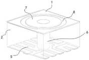
图1为本发明实施例1提供的三维阻抗网络双面加载的慢波基片集成波导的结构示意图;1 is a schematic structural diagram of a slow-wave substrate integrated waveguide loaded on both sides of a three-dimensional impedance network according to Embodiment 1 of the present invention;
图2为本发明实施例3提供的三维阻抗网络单元的结构示意图;2 is a schematic structural diagram of a three-dimensional impedance network unit provided in
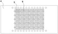
图3为本发明实施例2提供的慢波基片集成波导上表面的结构示意图;3 is a schematic structural diagram of the upper surface of the slow-wave substrate integrated waveguide provided in
图4为本发明实施例1提供的慢波基片集成波导下表面的结构示意图;4 is a schematic structural diagram of the lower surface of the slow-wave substrate integrated waveguide provided in Embodiment 1 of the present invention;
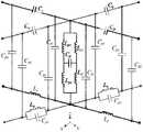
图5为本发明实施例3提供的三维慢波阻抗网络等效电路示意图;5 is a schematic diagram of an equivalent circuit of a three-dimensional slow-wave impedance network provided in
图6为本发明实施例3提供的三维慢波阻抗网络等效电路简化示意图;6 is a simplified schematic diagram of an equivalent circuit of a three-dimensional slow-wave impedance network provided in
图7为本发明实施例3提供的三维阻抗网络双面加载的慢波基片集成波导的等效电路模型示意图;7 is a schematic diagram of an equivalent circuit model of a slow-wave substrate integrated waveguide loaded on both sides of a three-dimensional impedance network according to
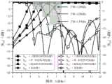
图8为本发明实施例4提供的三种不同网络加载的SW-SIW和传统SIW的传输模型仿真结果示意图;FIG. 8 is a schematic diagram of simulation results of transmission models of SW-SIW and traditional SIW loaded by three different networks according to
图标:1-上表面金属敷层,2-介质基片,3-金属化通孔阵列,4-下表面金属敷层,5-蛇形阻抗网络,6-金属化通孔,7-圆形金属贴片,8-环形槽,9-梯形过渡段。Icons: 1- Top metallization, 2-Dielectric substrate, 3-Metalized via array, 4-Bottom metallization, 5-Snake impedance network, 6-Metalized via, 7-Circular Metal patch, 8-ring groove, 9- trapezoidal transition.
具体实施方式Detailed ways
为使本发明实施例的目的、技术方案和优点更加清楚,下面将结合本发明实施例中的附图,对本发明实施例中的技术方案进行清楚、完整地描述,显然,所描述的实施例是本发明一部分实施例,而不是全部的实施例。通常在此处附图中描述和示出的本发明实施例的组件可以以各种不同的配置来布置和设计。In order to make the purposes, technical solutions and advantages of the embodiments of the present invention clearer, the technical solutions in the embodiments of the present invention will be clearly and completely described below with reference to the accompanying drawings in the embodiments of the present invention. Obviously, the described embodiments These are some embodiments of the present invention, but not all embodiments. The components of the embodiments of the invention generally described and illustrated in the drawings herein may be arranged and designed in a variety of different configurations.
实施例1Example 1
参阅图1所示的三维阻抗网络双面加载的慢波基片集成波导,包括介质基片,所述介质基片的上下两个表面为金属敷层且介质基片两侧设置有金属化通孔阵列,上表面金属敷层通过金属化通孔阵列穿过介质基片与下表面金属敷层相连。Referring to the slow-wave substrate integrated waveguide with double-sided loading of the three-dimensional impedance network shown in FIG. 1, it includes a dielectric substrate, the upper and lower surfaces of the dielectric substrate are metal cladding layers, and metallization holes are arranged on both sides of the dielectric substrate. A hole array, the upper surface metal coating layer is connected to the lower surface metal coating layer through the dielectric substrate through the metallized through hole array.
所述介质基片的上表面金属敷层上设置有N个与其通过缺口电气连接的金属贴片,N个金属贴片、缺口和金属化通孔的组合构成环-伞形立体阻抗网络,每个组合(环-伞阻抗单元)均包括一金属贴片和一与所述金属贴片连接的金属化通孔,其中,N为大于等于1的正整数,所述金属化通孔连接设置在下表面金属敷层的蛇形阻抗网络;The metal coating layer on the upper surface of the dielectric substrate is provided with N metal patches electrically connected with it through the notch. Each combination (ring-umbrella impedance unit) includes a metal patch and a metallized through hole connected to the metal patch, where N is a positive integer greater than or equal to 1, and the metallized through hole is connected to the bottom Serpentine impedance network of surface metal coating;
参阅图4所示的下表面结构,所述蛇形阻抗网络由N个横向蛇形线以及与其连接的纵向微带线的组合构成,每个组合(蛇形阻抗单元)均包括一横向蛇形线和一与所述横向蛇形线连接的纵向微带线,其中,相邻的所述横向蛇形线以及纵向微带线对应连接,使下表面金属敷层整体达到电气连接;所述金属化通孔垂直连接于横向蛇形线与纵向微带线的横纵向交叉处,构成三维阻抗网络单元。Referring to the lower surface structure shown in FIG. 4 , the serpentine impedance network is composed of a combination of N transverse serpentine lines and vertical microstrip lines connected thereto, and each combination (serpentine impedance unit) includes a transverse serpentine line and a vertical microstrip line connected to the transverse serpentine line, wherein the adjacent transverse serpentine lines and the vertical microstrip line are connected correspondingly, so that the metal coating on the lower surface is electrically connected as a whole; the metal The through holes are vertically connected to the transverse and longitudinal intersections of the transverse serpentine line and the longitudinal microstrip line to form a three-dimensional impedance network unit.
当N为1时,上表面的组合直接通过金属化过孔连接下表面组合的横纵向交叉处。采用该结构的基片集成波导,其性能、慢波效应不佳。为了增强其性能和慢波效应,N取较大值。When N is 1, the combination of the upper surface is directly connected to the transverse and longitudinal intersection of the combination of the lower surface through metallized vias. The substrate integrated waveguide using this structure has poor performance and slow wave effect. In order to enhance its performance and slow wave effect, N takes a larger value.
需要说明的是,本实施例通过上表面的组合可捕获原本位于基片集成波导中部的电场,从而极大增强了基片集成波导上表面的电容效应。对于磁场而言,下表面的组合能够引发磁场沿着横向蛇形线及纵向微带线在下表面集中,从而有效的实现了磁场向下剥离。综上,本实施例的三维阻抗网络双面加载的慢波能够实现电场和磁场的双向分离,获得了更强烈的慢波效应;从而能够减小横向尺寸,获得更良好的小型化效果。It should be noted that, in this embodiment, the electric field originally located in the middle of the substrate-integrated waveguide can be captured by the combination of the upper surfaces, thereby greatly enhancing the capacitive effect on the upper surface of the substrate-integrated waveguide. For the magnetic field, the combination of the lower surface can induce the magnetic field to concentrate on the lower surface along the transverse serpentine line and the longitudinal microstrip line, thereby effectively realizing the downward stripping of the magnetic field. To sum up, the slow wave loaded on both sides of the three-dimensional impedance network in this embodiment can realize bidirectional separation of electric field and magnetic field, and obtain a stronger slow wave effect; thus, the lateral size can be reduced, and a better miniaturization effect can be obtained.
实施例2Example 2
本实施例在上述实施例的基础上对环-伞形立体阻抗网络的结构做了优化。This embodiment optimizes the structure of the ring-umbrella three-dimensional impedance network on the basis of the above-mentioned embodiment.
环-伞形立体阻抗网络在上表面金属敷层与金属敷层共同构成矩形加载区域;参阅图3所示的上表面结构中的组合结构所示,金属贴片为圆形,缺口对应设置为环形;具体的,受标准PCB加工工艺精度的限制,环形槽宽度需不小于0.05mm,且宽度越小,慢波效果越好;圆形金属贴片直径须大于金属化通孔的直径,在一种实施方式中,金属化通孔的直径为0.5mm。进一步的,所述金属化通孔连接于所述圆形金属贴片的中心位置。环-伞形立体阻抗网络包括多个沿矩形加载区域依次排列的组合;例如沿横向构成单排结构/多排结构,沿纵向构成单排结构/多排结构;此外,组合也可以采用周期排列的多排多列结构,例如组合沿横向设置有多排且沿纵向设置有多列;相邻组合通过其横向边沿或纵向边沿直接连接,也可以通过其余介质材料实现电气连接。附图中并未给出该结构的示例。The ring-umbrella-shaped three-dimensional impedance network forms a rectangular loading area on the upper surface of the metal coating and the metal coating; referring to the combined structure in the upper surface structure shown in Figure 3, the metal patch is circular, and the gap is correspondingly set as Ring; specifically, limited by the precision of standard PCB processing technology, the width of the annular groove should not be less than 0.05mm, and the smaller the width, the better the slow wave effect; the diameter of the circular metal patch must be larger than the diameter of the metallized through hole. In one embodiment, the diameter of the metallized via is 0.5 mm. Further, the metallized through hole is connected to the center of the circular metal patch. The ring-umbrella three-dimensional impedance network includes a plurality of combinations arranged in sequence along the rectangular loading area; for example, a single-row structure/multi-row structure is formed in the transverse direction, and a single-row structure/multi-row structure is formed in the longitudinal direction; in addition, the combination can also be arranged periodically The multi-row multi-column structure, for example, the combination is provided with multiple rows in the transverse direction and multiple columns in the longitudinal direction; the adjacent combinations are directly connected by their transverse or longitudinal edges, and can also be electrically connected through the remaining dielectric materials. An example of this structure is not shown in the drawings.
采用该结构的基片集成波导,其上表面的电容效应不佳。为了增强上表面的电容效应,需要重设计环-伞形立体阻抗网络的组合排列。The substrate-integrated waveguide using this structure has poor capacitance effect on the upper surface. To enhance the capacitive effect of the upper surface, the combined arrangement of the ring-umbrella stereo impedance network needs to be redesigned.
进一步的,参阅图3所示的上表面结构,环-伞形立体阻抗网络中各组合间隔设置,各组合的间距需小于四分之一导波波长,彼此间通过金属敷层电气连接。Further, referring to the upper surface structure shown in FIG. 3, each combination in the ring-umbrella three-dimensional impedance network is arranged at intervals, and the spacing of each combination should be less than a quarter of the guided wave wavelength, and they are electrically connected to each other through a metal coating.
经实验研究,基于上述思想,发明人研发了一种能够在慢波效应和小型化结构上均有良好效果的结构。详见下实施例。Through experimental research and based on the above-mentioned idea, the inventor has developed a structure that can have good effects on both the slow-wave effect and the miniaturized structure. See the examples below for details.
实施例3Example 3
基于上述结构,上表面金属敷层和下表面金属敷层采用敷铜工艺,介质基片的厚度为0.1~5mm,所述上表面金属敷层和下表面金属敷层的厚度为0.01~0.05mm;在一种实施方式中,铜厚度均为0.035mm,介质基片则选用厚度为1.016mm的板材为最优选项。上表面铜层采用标准PCB工艺加工蚀刻成中空矩形与矩形内环-伞形立体阻抗网络的组合,二者共同构成矩形加载区域。矩形加载区域的两端分别通过一梯形过渡段与输入端和输出端微带线相连;其中,所述输入端和输出端微带线的特性阻抗均为50Ω。Based on the above structure, the metal coating on the upper surface and the metal coating on the lower surface adopt the copper coating process, the thickness of the dielectric substrate is 0.1-5 mm, and the thickness of the metal coating on the upper surface and the metal coating on the lower surface is 0.01-0.05mm ; In an embodiment, the copper thickness is 0.035mm, and the dielectric substrate is a plate with a thickness of 1.016mm as the best option. The copper layer on the upper surface is processed and etched into a combination of a hollow rectangle and a rectangular inner ring-umbrella three-dimensional impedance network using a standard PCB process, and the two together form a rectangular loading area. Two ends of the rectangular loading area are respectively connected with the input end and the output end microstrip line through a trapezoidal transition section; wherein, the characteristic impedance of the input end and the output end microstrip line are both 50Ω.
矩形加载区域中各组合通过上表面铜层彼此间隔小于四分之一导波波长的间距相连,环-伞形立体阻抗网络通过焊接与中空矩形铜层连接,使介质基片上表面金属铜层整体达到电气连接。Each combination in the rectangular loading area is connected to each other by the copper layer on the upper surface with a spacing smaller than a quarter of the guided wave wavelength, and the ring-umbrella three-dimensional impedance network is connected to the hollow rectangular copper layer by welding, so that the metal copper layer on the upper surface of the dielectric substrate is integrated as a whole. achieve electrical connection.
下表面铜层采用标准PCB工艺加工蚀刻成中空矩形与矩形内蛇形阻抗网络的组合,将所有相邻的组合中横向蛇形线与纵向微带线所构成的蛇形阻抗网络,以及中空矩形铜层的四边对应连接起来,使介质基片下表面金属铜层整体达到电气连接。The copper layer on the lower surface is processed and etched into a combination of a hollow rectangle and a serpentine impedance network in the rectangle by standard PCB process. The four sides of the copper layer are connected correspondingly, so that the whole metal copper layer on the lower surface of the dielectric substrate is electrically connected.
基于图3和图4的上表面环-伞阻抗网络的组合和下表面蛇形阻抗网络的组合所构成的三维阻抗网络单元,可以得到如图7所示的三维阻抗网络双面加载的慢波的等效电路模型。Based on the three-dimensional impedance network unit formed by the combination of the upper surface loop-umbrella impedance network and the combination of the lower surface serpentine impedance network shown in Figure 3 and Figure 4, the slow wave loaded on both sides of the three-dimensional impedance network as shown in Figure 7 can be obtained. equivalent circuit model.
本实施例通过三维阻抗网络的方式,产生慢波效应,同时有效降低了横向和纵向尺寸,实现了显著降低基片集成波导尺寸的效果。且本基片集成波导,基于成熟的PCB制造技术和SMT工艺,体积小,易于制作和大批量生产。In this embodiment, the slow wave effect is generated by means of a three-dimensional impedance network, and the lateral and vertical dimensions are effectively reduced, and the effect of significantly reducing the dimensions of the substrate integrated waveguide is achieved. And this substrate integrated waveguide, based on mature PCB manufacturing technology and SMT process, is small in size, easy to manufacture and mass-produced.
下面以一个基于该结构,介质基片采用Rogers Kappa 438,相对介电常数为4.38,介质损耗角正切为0.005,厚度为1.016mm,上下表面金属敷层为铜,厚度为0.035mm;截止频率在3.91GHz附近。通带范围内,带内插损为0.69dB-0.77dB,回波损耗优于20dB的基片集成波导设计为例,具体说明相关内容。该慢波结构示意图如图1所示,三维阻抗网络单元如图2所示,其中,Cx、Cy表示上表面金属敷层与圆形金属贴片之间的增强电容;Lpz表示由金属化通孔带来的寄生电感;Cp表示金属化通孔内壁带来的寄生电容;Cpz表示上表面金属敷层以及圆形金属贴片与下表面组合之间产生的寄生电容;Lx、Ly分别表示下表面组合中的横向蛇形线和纵向微带线增强电感;Cpx表示下表面组合自身产生的寄生电容。需要说明的是,上表面金属敷层为了容纳除导波方向电流以外的对冲电流,沿金属化通孔会形成径向电流路径,所以该路径感应处的寄生电感Lpz不可省略。对于产生的寄生电容Cp、Cpz、Cpx,其数值远小于增强电容Cx、Cy的数值,所以图5能够简化为图6,得到简化后的三维阻抗网络单元等效电路。Based on this structure, the dielectric substrate is made of Rogers Kappa 438, the relative dielectric constant is 4.38, the dielectric loss tangent is 0.005, the thickness is 1.016mm, and the metal coating on the upper and lower surfaces is copper, with a thickness of 0.035mm; the cut-off frequency is at Near 3.91GHz. In the passband range, the insertion loss in the band is 0.69dB-0.77dB, and the return loss is better than 20dB. The schematic diagram of the slow-wave structure is shown in Figure 1, and the three-dimensional impedance network unit is shown in Figure 2, where Cx and Cy represent the enhanced capacitance between the upper surface metal coating and the circular metal patch; Lpz represents the Parasitic inductance caused by metallized through holes; Cp represents the parasitic capacitance caused by the inner wall of the metallized through hole; Cpz represents the parasitic capacitance generated between the upper surface metal coating and the combination of the circular metal patch and the lower surface; Lx andLy respectively represent the enhanced inductance of the transverse serpentine line and the vertical microstrip line in the lower surface combination; Cpx represents the parasitic capacitance generated by the lower surface combination itself. It should be noted that, in order to accommodate the rush current except the current in the guided wave direction, the metallization layer on the upper surface will form a radial current path along the metallized through hole, so the parasitic inductance Lpz induced by the path cannot be omitted. For the generated parasitic capacitances Cp , Cpz , and Cpx , the values are much smaller than the values of the enhancement capacitances Cx and Cy , so FIG. 5 can be simplified as FIG. 6 , and the simplified equivalent circuit of the three-dimensional impedance network unit is obtained.
在本实施例中,电场和磁场的分离是加载环-伞形立体阻抗网络和蛇形阻抗网络促成的。其中,上表面包围圆形金属贴片的金属敷层对应于传统基片集成波导的上表面,由上表面金属敷层包围的圆形金属贴片实际上是通过金属化过孔连接升高的接地面。该结构由于电场被金属化通孔顶部的圆形金属贴片与上表面金属敷层之间的环形槽捕获,所以使原本位于基片集成波导中部的电场集中在增强电容Cx、Cy周围,从而极大增强了基片集成波导上表面的电容效应。In this embodiment, the separation of the electric and magnetic fields is facilitated by the loading ring-umbrella stereo impedance network and the serpentine impedance network. Among them, the metal coating surrounded by the circular metal patch on the upper surface corresponds to the upper surface of the traditional substrate integrated waveguide, and the circular metal patch surrounded by the metal coating on the upper surface is actually raised by metallized vias. ground plane. In this structure, since the electric field is captured by the annular groove between the circular metal patch on the top of the metallized via and the metal coating on the upper surface, the electric field originally located in the middle of the integrated waveguide of the substrate is concentrated around the enhanced capacitors Cx and Cy , thereby greatly enhancing the capacitance effect on the upper surface of the substrate integrated waveguide.
横向蛇形线及其纵向连接的纵向微带线构成的组合等效为增强电感Lx、Ly。对于磁场而言,下表面组合等效的增强电感Lx、Ly带来额外的表面电流路径,引发磁场沿着该组合在下表面集中,有效的实现了磁场向下剥离。从而本实施例的三维阻抗网络单元表现出强烈的慢波效应。The combination formed by the transverse serpentine line and its longitudinally connected longitudinal microstrip lines is equivalent to enhanced inductance Lx ,Ly . For the magnetic field, the combination of equivalent enhanced inductances Lx and Ly on the lower surface brings additional surface current paths, causing the magnetic field to concentrate on the lower surface along the combination, effectively realizing the downward stripping of the magnetic field. Therefore, the three-dimensional impedance network unit of this embodiment exhibits a strong slow wave effect.
进一步的,本实施例以下将传统的SIW传输线、下表面蛇形网络加载型SW-SIW传输线、环-伞形阵列加载型SW-SIW传输线与本实施例的三维阻抗网络双面加载的SW-SIW传输线进行比较。Further, in this embodiment, the traditional SIW transmission line, the lower surface serpentine network loaded SW-SIW transmission line, the ring-umbrella array loaded SW-SIW transmission line and the three-dimensional impedance network double-sided loaded SW-SIW transmission line of this embodiment are used in the following. SIW transmission line for comparison.
参阅图8所示,示出了三种不同网络加载的SW-SIW和传统SIW的传输模型仿真结果,可以看出基于三维阻抗网络双面加载的SW-SIW的截止频率在3.91GHz附近。通带范围内,带内插损为0.69dB-0.77dB,回波损耗优于20dB。综上所述,如果采用传统SIW结构来实现截止频率相同的传输线,在介质基片材料完全相同的情况下,传统SIW结构的物理宽度为18.5mm。基于三维阻抗网络双面加载的SW-SIW的横向宽度较少了约40%。即,本实施例的三维阻抗网络双面加载的慢波能够减小横向尺寸,获得良好的小型化效果。Referring to Figure 8, which shows the simulation results of the transmission model of SW-SIW loaded with three different networks and traditional SIW, it can be seen that the cut-off frequency of SW-SIW loaded on both sides of the three-dimensional impedance network is around 3.91 GHz. In the passband range, the intraband insertion loss is 0.69dB-0.77dB, and the return loss is better than 20dB. To sum up, if the traditional SIW structure is used to realize the transmission line with the same cut-off frequency, the physical width of the traditional SIW structure is 18.5mm under the condition of the same dielectric substrate material. The lateral width of the SW-SIW based on the double-sided loading of the 3D impedance network is reduced by about 40%. That is, the slow wave loaded on both sides of the three-dimensional impedance network of the present embodiment can reduce the lateral size and obtain a good miniaturization effect.
本实施例还提供上述三维阻抗网络双面加载的慢波的设计方法包括:This embodiment also provides the above-mentioned design method for slow waves loaded on both sides of the three-dimensional impedance network, including:
步骤1:由实际需要的导波波长确定基片集成波导介质基片的微波介质材料;Step 1: Determine the microwave dielectric material of the substrate-integrated waveguide dielectric substrate according to the actual required waveguide wavelength;
步骤2:在介质基片的上下两个表面两侧设置金属化通孔阵列,连接介质基片的上、下表面金属敷层;Step 2: arrange metallized through hole arrays on both sides of the upper and lower surfaces of the dielectric substrate to connect the metal coating layers on the upper and lower surfaces of the dielectric substrate;
步骤3:对介质基片的环-伞形单元进行设计,利用电磁仿真软件建模环-伞形立体阻抗网络;Step 3: Design the ring-umbrella unit of the dielectric substrate, and use electromagnetic simulation software to model the ring-umbrella three-dimensional impedance network;
步骤4:对介质基片下表面金属敷层的蛇形阻抗单元进行设计,将所有相邻的蛇形阻抗单元连接,使介质基片下表面金属敷层整体达到电气连接,利用电磁仿真软件建模蛇形阻抗网络;Step 4: Design the serpentine impedance unit of the metal coating on the lower surface of the dielectric substrate, connect all adjacent serpentine impedance units, so that the metal coating on the lower surface of the dielectric substrate can be electrically connected as a whole. Modular serpentine impedance network;
步骤5:对基片集成波导进行微带过渡设计,在其上表面金属敷层的两端加入梯形过渡段,通过调整梯形过渡段的特性,实现对微带线与基片集成波导之间的驻波情况的调整。Step 5: Design the microstrip transition for the substrate integrated waveguide, add trapezoidal transition sections at both ends of the metal coating on its upper surface, and adjust the characteristics of the trapezoidal transition section to realize the transition between the microstrip line and the substrate integrated waveguide. Adjustment for standing wave conditions.
以上仅为本发明的优选实施例而已,并不用于限制本发明,对于本领域的技术人员来说,本发明可以有各种更改和变化。凡在本发明的精神和原则之内,所作的任何修改、等同替换、改进等,均应包含在本发明的保护范围之内。The above are only preferred embodiments of the present invention, and are not intended to limit the present invention. For those skilled in the art, the present invention may have various modifications and changes. Any modification, equivalent replacement, improvement, etc. made within the spirit and principle of the present invention shall be included within the protection scope of the present invention.
Claims (10)
Priority Applications (1)
| Application Number | Priority Date | Filing Date | Title |
|---|---|---|---|
| CN202110553726.8ACN113285197B (en) | 2021-05-20 | 2021-05-20 | Three-dimensional impedance network double-side loaded slow wave substrate integrated waveguide and design method thereof |
Applications Claiming Priority (1)
| Application Number | Priority Date | Filing Date | Title |
|---|---|---|---|
| CN202110553726.8ACN113285197B (en) | 2021-05-20 | 2021-05-20 | Three-dimensional impedance network double-side loaded slow wave substrate integrated waveguide and design method thereof |
Publications (2)
| Publication Number | Publication Date |
|---|---|
| CN113285197A CN113285197A (en) | 2021-08-20 |
| CN113285197Btrue CN113285197B (en) | 2022-04-15 |
Family
ID=77280489
Family Applications (1)
| Application Number | Title | Priority Date | Filing Date |
|---|---|---|---|
| CN202110553726.8AActiveCN113285197B (en) | 2021-05-20 | 2021-05-20 | Three-dimensional impedance network double-side loaded slow wave substrate integrated waveguide and design method thereof |
Country Status (1)
| Country | Link |
|---|---|
| CN (1) | CN113285197B (en) |
Families Citing this family (2)
| Publication number | Priority date | Publication date | Assignee | Title |
|---|---|---|---|---|
| CN113889737B (en)* | 2021-09-30 | 2022-04-08 | 西华大学 | Substrate integrated waveguide parameter optimization method and structure based on reinforcement learning |
| CN115513622B (en)* | 2022-11-03 | 2023-07-04 | 西华大学 | Quarter-mode slow-wave substrate integrated waveguide filter |
Citations (4)
| Publication number | Priority date | Publication date | Assignee | Title |
|---|---|---|---|---|
| WO2016058627A1 (en)* | 2014-10-13 | 2016-04-21 | Gapwaves Ab | A microwave or millimeter wave rf part assembled with pick-and-place technology |
| CN106654497A (en)* | 2017-01-03 | 2017-05-10 | 电子科技大学 | Miniaturized broadband slow-wave half-mode substrate-integrated waveguide coupler and design method thereof |
| CN106887661A (en)* | 2017-03-15 | 2017-06-23 | 电子科技大学 | Slow wave substrate integration wave-guide based on the loading of lumped parameter inductance |
| CN112072249A (en)* | 2020-07-20 | 2020-12-11 | 西安电子科技大学 | A broadband slow-wave substrate integrated waveguide with high slow-wave coefficient |
Family Cites Families (1)
| Publication number | Priority date | Publication date | Assignee | Title |
|---|---|---|---|---|
| CN110752430B (en)* | 2019-10-28 | 2021-06-29 | 南京邮电大学 | Miniaturized slow-wave half-mode substrate integrated waveguide E-plane coupler |
- 2021
- 2021-05-20CNCN202110553726.8Apatent/CN113285197B/enactiveActive
Patent Citations (4)
| Publication number | Priority date | Publication date | Assignee | Title |
|---|---|---|---|---|
| WO2016058627A1 (en)* | 2014-10-13 | 2016-04-21 | Gapwaves Ab | A microwave or millimeter wave rf part assembled with pick-and-place technology |
| CN106654497A (en)* | 2017-01-03 | 2017-05-10 | 电子科技大学 | Miniaturized broadband slow-wave half-mode substrate-integrated waveguide coupler and design method thereof |
| CN106887661A (en)* | 2017-03-15 | 2017-06-23 | 电子科技大学 | Slow wave substrate integration wave-guide based on the loading of lumped parameter inductance |
| CN112072249A (en)* | 2020-07-20 | 2020-12-11 | 西安电子科技大学 | A broadband slow-wave substrate integrated waveguide with high slow-wave coefficient |
Non-Patent Citations (3)
| Title |
|---|
| Broadband mm-wave propagation characterization of planar groove gap waveguide;Titus Oyedokun et al.;《Microw Opt Technol Lett.》;20201230;第1-5页* |
| Metallized Blind Via Holes and Surface Etching Incorporation for Miniaturization Enhancement in Slow-wave Substrate Integrated Waveguide;Yuliang Zhou et al.;《2019 Photonics & Electromagnetics Research Symposium - Fall (PIERS - Fall)》;20200305;第1224-1227页* |
| Slow-Wave Effect Enhanced Substrate Integrated Waveguide with Multi-Antipodal Blind Via-Holes and Distributed Metal Strips;Yuliang Zhou et al.;《IEEE Microwave and Wireless Components Letters》;20200701;第753-756页* |
Also Published As
| Publication number | Publication date |
|---|---|
| CN113285197A (en) | 2021-08-20 |
Similar Documents
| Publication | Publication Date | Title |
|---|---|---|
| CN115777161B (en) | Multilayer waveguide with metasurface, arrangement thereof and method of production | |
| KR100349571B1 (en) | Resonator Using Defected Ground Structure on Dielectric | |
| US6617943B1 (en) | Package substrate interconnect layout for providing bandpass/lowpass filtering | |
| CN108172958B (en) | Periodic slow wave transmission line unit based on coplanar waveguide | |
| CN106887661B (en) | Slow wave substrate integration wave-guide based on the load of lumped parameter inductance | |
| KR20090092706A (en) | System for interconnecting two substrates each comprising at least one transmission line | |
| JP5466340B2 (en) | Coupling mechanism for microwave reentrant resonant cavity attached to PCB | |
| CN113285197B (en) | Three-dimensional impedance network double-side loaded slow wave substrate integrated waveguide and design method thereof | |
| CN108777343A (en) | Substrate integration wave-guide transmission structure, antenna structure and connection method | |
| CN208173765U (en) | Substrate integration wave-guide transmission structure, antenna structure | |
| CN106654497B (en) | Miniaturized broadband slow-wave half-mode substrate-integrated waveguide coupler and its design method | |
| US8179204B2 (en) | Bandgap impedance surface of polar configuration usable in a waveguide transition module | |
| CN102709658B (en) | Half mode double-ridge substrate integrated waveguide with transitional balanced micro-strip lines | |
| CN112768857A (en) | Serial six-order substrate integrated waveguide cross-coupling filter | |
| CN115693063A (en) | Miniature substrate integrated waveguide filter with internal ripple suppression | |
| US7002433B2 (en) | Microwave coupler | |
| CN210006879U (en) | Miniaturized broadband coupler of thin film integration technology | |
| CN105720330A (en) | Novel complementary split-ring resonator structure-based substrate integrated waveguide band-pass filter | |
| WO2025139847A1 (en) | Circularly polarized array antenna and wireless communication device | |
| CN204885390U (en) | A double-layer miniaturized low-cost directional branch coupler | |
| CN118472580A (en) | Slow-wave HMSIW dual-frequency filter power divider loaded with complementary serpentine split ring and its design method | |
| CN103515680A (en) | Dual-mode band-pass filter and multi-order band-pass filter formed by the same | |
| KR20210032113A (en) | Transition structure between microstrip and hollow substrate integrated waveguide | |
| Khalil et al. | Compact SIW leaky wave antenna | |
| Maloratsky | Microstrip circuits with a modified ground plane |
Legal Events
| Date | Code | Title | Description |
|---|---|---|---|
| PB01 | Publication | ||
| PB01 | Publication | ||
| SE01 | Entry into force of request for substantive examination | ||
| SE01 | Entry into force of request for substantive examination | ||
| GR01 | Patent grant | ||
| GR01 | Patent grant |