CN113193333B - Fractal structure on-chip antenna applied to CMOS (complementary Metal oxide semiconductor) process - Google Patents
Fractal structure on-chip antenna applied to CMOS (complementary Metal oxide semiconductor) processDownload PDFInfo
- Publication number
- CN113193333B CN113193333BCN202110475059.6ACN202110475059ACN113193333BCN 113193333 BCN113193333 BCN 113193333BCN 202110475059 ACN202110475059 ACN 202110475059ACN 113193333 BCN113193333 BCN 113193333B
- Authority
- CN
- China
- Prior art keywords
- antenna
- patch
- fractal
- diamond
- cut
- Prior art date
- Legal status (The legal status is an assumption and is not a legal conclusion. Google has not performed a legal analysis and makes no representation as to the accuracy of the status listed.)
- Active
Links
- 238000000034methodMethods0.000titleclaimsabstractdescription15
- 230000000295complement effectEffects0.000titleabstract2
- 229910044991metal oxideInorganic materials0.000titleabstract2
- 150000004706metal oxidesChemical class0.000titleabstract2
- 239000004065semiconductorSubstances0.000titleabstract2
- 239000004020conductorSubstances0.000claimsabstractdescription31
- 230000005855radiationEffects0.000claimsabstractdescription12
- 239000000758substrateSubstances0.000claimsabstractdescription10
- 238000002161passivationMethods0.000claimsabstractdescription9
- XUIMIQQOPSSXEZ-UHFFFAOYSA-NSiliconChemical compound[Si]XUIMIQQOPSSXEZ-UHFFFAOYSA-N0.000claimsabstractdescription8
- 229910052710siliconInorganic materials0.000claimsabstractdescription8
- 239000010703siliconSubstances0.000claimsabstractdescription8
- 229910003460diamondInorganic materials0.000claimsdescription26
- 239000010432diamondSubstances0.000claimsdescription26
- 239000002184metalSubstances0.000claimsdescription14
- VYPSYNLAJGMNEJ-UHFFFAOYSA-NSilicium dioxideChemical compoundO=[Si]=OVYPSYNLAJGMNEJ-UHFFFAOYSA-N0.000claimsdescription11
- 238000005516engineering processMethods0.000claimsdescription9
- 239000000919ceramicSubstances0.000claimsdescription5
- 235000012239silicon dioxideNutrition0.000claimsdescription5
- 239000000377silicon dioxideSubstances0.000claimsdescription5
- 239000011159matrix materialSubstances0.000claimsdescription3
- 239000011295pitchSubstances0.000claims1
- 238000004891communicationMethods0.000abstractdescription8
- 230000008054signal transmissionEffects0.000abstractdescription3
- 230000002349favourable effectEffects0.000abstract1
- 238000010586diagramMethods0.000description5
- 230000010354integrationEffects0.000description3
- 238000001228spectrumMethods0.000description3
- 238000004519manufacturing processMethods0.000description2
- 230000009286beneficial effectEffects0.000description1
- 230000005540biological transmissionEffects0.000description1
- 230000000694effectsEffects0.000description1
- 230000005672electromagnetic fieldEffects0.000description1
- 238000003384imaging methodMethods0.000description1
- 238000000059patterningMethods0.000description1
- 229910052814silicon oxideInorganic materials0.000description1
Images


Classifications
- H—ELECTRICITY
- H01—ELECTRIC ELEMENTS
- H01Q—ANTENNAS, i.e. RADIO AERIALS
- H01Q1/00—Details of, or arrangements associated with, antennas
- H01Q1/12—Supports; Mounting means
- H01Q1/22—Supports; Mounting means by structural association with other equipment or articles
- H01Q1/2283—Supports; Mounting means by structural association with other equipment or articles mounted in or on the surface of a semiconductor substrate as a chip-type antenna or integrated with other components into an IC package
- H—ELECTRICITY
- H01—ELECTRIC ELEMENTS
- H01Q—ANTENNAS, i.e. RADIO AERIALS
- H01Q1/00—Details of, or arrangements associated with, antennas
- H01Q1/36—Structural form of radiating elements, e.g. cone, spiral, umbrella; Particular materials used therewith
- H01Q1/38—Structural form of radiating elements, e.g. cone, spiral, umbrella; Particular materials used therewith formed by a conductive layer on an insulating support
- H—ELECTRICITY
- H01—ELECTRIC ELEMENTS
- H01Q—ANTENNAS, i.e. RADIO AERIALS
- H01Q15/00—Devices for reflection, refraction, diffraction or polarisation of waves radiated from an antenna, e.g. quasi-optical devices
- H01Q15/14—Reflecting surfaces; Equivalent structures
- H—ELECTRICITY
- H01—ELECTRIC ELEMENTS
- H01Q—ANTENNAS, i.e. RADIO AERIALS
- H01Q23/00—Antennas with active circuits or circuit elements integrated within them or attached to them
- H—ELECTRICITY
- H01—ELECTRIC ELEMENTS
- H01Q—ANTENNAS, i.e. RADIO AERIALS
- H01Q5/00—Arrangements for simultaneous operation of antennas on two or more different wavebands, e.g. dual-band or multi-band arrangements
- H01Q5/10—Resonant antennas
- H—ELECTRICITY
- H01—ELECTRIC ELEMENTS
- H01Q—ANTENNAS, i.e. RADIO AERIALS
- H01Q9/00—Electrically-short antennas having dimensions not more than twice the operating wavelength and consisting of conductive active radiating elements
- H01Q9/04—Resonant antennas
- H01Q9/0485—Dielectric resonator antennas
Landscapes
- Engineering & Computer Science (AREA)
- Microelectronics & Electronic Packaging (AREA)
- Physics & Mathematics (AREA)
- Electromagnetism (AREA)
- Waveguide Aerials (AREA)
Abstract
Description
Translated fromChinese技术领域technical field
本发明属于无线通信技术领域,涉及毫米波集成电路和片上天线技术,特别提供一种基于CMOS工艺的应用于毫米波频段的同时加载人工磁导体和介质谐振器的分形结构片上天线。The invention belongs to the technical field of wireless communication, relates to millimeter-wave integrated circuits and on-chip antenna technology, and particularly provides a fractal structure on-chip antenna based on CMOS technology and applied to a millimeter-wave frequency band and loaded with artificial magnetic conductors and dielectric resonators at the same time.
背景技术Background technique
随着无线通信技术的迅速发展以及智能终端的大范围普及,低频段的资源被大量使用,这使得无线通信系统分配的频谱资源变得日益拥挤,系统容量变得日益匮乏,为了解决系统容量匮乏以及频谱资源短缺问题,研究者们将目光转向了更加广阔的毫米波段。作为收发射频信号的无源器件,天线是通信系统的核心,如何增加天线的频谱数据传输量是毫米波通信发展的重大挑战。57~64GHz是目前最热门的毫米波频段之一,适用于高带宽短距离无线通信系统;这样的高频下天线的尺寸较小,极为适合与芯片集成在一起,而CMOS工艺提供了这样一个集成的平台。With the rapid development of wireless communication technology and the widespread popularization of intelligent terminals, the resources of the low frequency band are used in large quantities, which makes the spectrum resources allocated by the wireless communication system become increasingly crowded and the system capacity becomes increasingly scarce. In order to solve the lack of system capacity As well as the shortage of spectrum resources, researchers turned their attention to the wider millimeter waveband. As a passive device that transmits and receives radio frequency signals, the antenna is the core of the communication system. How to increase the spectrum data transmission capacity of the antenna is a major challenge for the development of millimeter wave communication. 57-64GHz is one of the most popular millimeter-wave frequency bands, suitable for high-bandwidth short-distance wireless communication systems; the size of the antenna at such high frequencies is small, which is very suitable for integration with chips, and the CMOS process provides such a Integrated platform.
目前,将天线与芯片集成在一起的技术分为片上天线与封装天线两种,与封装天线相比,片上天线直接放置在芯片上,去除了芯片间互连线的影响,使得结构变得简单,降低了制造精度可靠性的需求,减小了集成的成本。片上天线作为毫米波频段的收发器,可以运用于成像以及短距离高频率的无线通信,但是,由于低阻抗硅衬底引入的损耗,导致现有片上天线的研究普遍存在低增益、低效率的现象,极大阻碍了片上天线的推广。At present, the technology of integrating the antenna and the chip is divided into two types: on-chip antenna and packaged antenna. Compared with packaged antenna, on-chip antenna is directly placed on the chip, which removes the influence of interconnecting lines between chips and simplifies the structure. , reducing the requirement of manufacturing accuracy and reliability, and reducing the cost of integration. As a transceiver in the millimeter wave band, the on-chip antenna can be used in imaging and short-distance high-frequency wireless communication. However, due to the loss introduced by the low-impedance silicon substrate, the existing research on on-chip antennas generally suffer from low gain and low efficiency. This phenomenon has greatly hindered the promotion of on-chip antennas.
发明内容SUMMARY OF THE INVENTION
本发明的目的在于针对现有毫米波频段(60GHz)片上天线存在的低增益、低效率的问题,提出了一种基于CMOS工艺的应用于毫米波频段的同时加载人工磁导体和介质谐振器的分形结构片上天线,用以提高天线的增益以及工作带宽。The purpose of the present invention is to solve the problems of low gain and low efficiency of the existing millimeter-wave band (60GHz) on-chip antennas, and propose a CMOS technology-based method for simultaneously loading artificial magnetic conductors and dielectric resonators in the millimeter-wave band. Fractal structure on-chip antenna to improve antenna gain and operating bandwidth.
为实现上述目的,本发明采用的技术方案在于:To achieve the above object, the technical scheme adopted in the present invention is:
一种应用于CMOS工艺的分形结构片上天线,包括:从下往上依次层叠的接地层1、硅衬底层2、二氧化硅层3及钝化层4;其特征在于,所述二氧化硅层3中设置有分形天线5与人工磁导体结构6,且人工磁导体结构6位于分形天线5的下方;所述钝化层4上还设置有介质谐振器7。A fractal structure on-chip antenna applied to a CMOS process, comprising: a
进一步的,所述分形天线5包括:辐射贴片8、馈线9以及GSG结构10,所述辐射贴片通过馈线连接到GSG焊盘的信号端;所述辐射贴片由共顶点设置的第五切角菱形贴片8-5、第四切角菱形贴片8-4、第二切角菱形贴片8-2、第一切角菱形贴片8-1与第三切角菱形贴片8-3沿顺时针方向依次拼接构成,每个切角菱形贴片的顶角均为72°,第五、第四、第三、第二切角菱形贴片的边长分别为第一切角菱形贴片的边长的5、4、3、2倍。Further, the
更进一步的,所述切角菱形贴片由菱形贴片沿顶角切扇形切角形成,扇形切角的圆心角为72°、且与菱形贴片的顶角重合,扇形切角的边长与菱形贴片的边长相等。Further, the corner-cut diamond patch is formed by cutting the fan-shaped cut corner along the top corner of the diamond-shaped patch. The sides of the rhombus patch are of equal length.
进一步的,所述人工磁导体结构6由若干个呈矩阵排列的人工磁导体单元6-1构成,且任意相邻人工磁导体单元间的间距相同。Further, the artificial
更进一步的,所述人工磁导体单元6-1呈正方形金属环状、且四角均切相同尺寸正方形切角,所述正方形切角的边长小于金属环的环宽。Further, the artificial magnetic conductor unit 6-1 is in the shape of a square metal ring, and all four corners are cut with square cut corners of the same size, and the side length of the square cut corner is smaller than the ring width of the metal ring.
进一步的,所述介质谐振器7为矩形陶瓷介质块。Further, the
本发明的有益效果在于:通过人工磁导体结构减小损耗硅衬底对于天线辐射性能的影响,并在天线顶层加上介质谐振器,实现天线增益和带宽的提高。The beneficial effect of the invention is that the influence of the lossy silicon substrate on the radiation performance of the antenna is reduced by the artificial magnetic conductor structure, and a dielectric resonator is added on the top layer of the antenna to improve the antenna gain and bandwidth.
本发明提供一种应用于毫米波频段的分形结构片上天线,该片上天线具有分形结构,拥有宽带宽特性,适用于多个频段的信号传输;同时,加载于分形天线下的人工磁导体结构具有实现电磁波全反射的效果,有助于减小电磁波在低阻高介电常数的硅衬底中的损耗,使得天线增益上升;加载于钝化层上的介质谐振器具有将电磁波向上方聚拢的作用,不但减小了衬底的损耗,还提升了天线辐射的方向性,使得天线增益提升;并且,该片上天线能够与CMOS工艺芯片集成,去除了芯片间互连线的影响,使得结构变得简单,降低了制造精度可靠性的需求,减小了集成的成本,简化了芯片间信号传输的匹配问题,同时极大的节省了系统占用的面积。The invention provides a fractal structure on-chip antenna applied to a millimeter wave frequency band. The on-chip antenna has a fractal structure, has wide bandwidth characteristics, and is suitable for signal transmission in multiple frequency bands; at the same time, the artificial magnetic conductor structure loaded under the fractal antenna has The effect of total reflection of electromagnetic waves is helpful to reduce the loss of electromagnetic waves in the silicon substrate with low resistance and high dielectric constant, which increases the antenna gain; the dielectric resonator loaded on the passivation layer has the ability to gather electromagnetic waves upward. It not only reduces the loss of the substrate, but also improves the directivity of the antenna radiation, so that the antenna gain is improved; and the on-chip antenna can be integrated with the CMOS process chip, which removes the influence of the interconnect lines between the chips and makes the structure change. It is simple, reduces the requirement of manufacturing accuracy and reliability, reduces the cost of integration, simplifies the matching problem of signal transmission between chips, and greatly saves the area occupied by the system.
综上,本发明提供一种基于CMOS工艺的应用于毫米波频段的同时加载人工磁导体和介质谐振器的分形结构片上天线,能够显著提高天线的增益以及工作带宽。In conclusion, the present invention provides a fractal structure on-chip antenna based on CMOS technology and applied to the millimeter wave frequency band and loaded with artificial magnetic conductors and dielectric resonators, which can significantly improve the gain and operating bandwidth of the antenna.
附图说明Description of drawings
图1为本发明应用于60GHz的分形结构片上天线的横截面结构示意图。FIG. 1 is a schematic cross-sectional structural diagram of a fractal structure on-chip antenna applied to 60 GHz according to the present invention.
图2为本发明中分形天线的结构示意图。FIG. 2 is a schematic structural diagram of a fractal antenna in the present invention.
图3为本发明中切角菱形贴片的结构示意图。FIG. 3 is a schematic structural diagram of a cut-angle diamond patch in the present invention.
图4为本发明中人工磁导体阵列的结构示意图。FIG. 4 is a schematic structural diagram of an artificial magnetic conductor array in the present invention.
图5为本发明中人工磁导体单元的结构示意图。FIG. 5 is a schematic structural diagram of an artificial magnetic conductor unit in the present invention.
图6为本发明实施例中分形结构片上天线的回波损耗曲线。FIG. 6 is the return loss curve of the fractal structure on-chip antenna in the embodiment of the present invention.
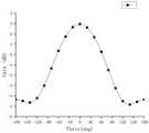
图7为本发明实施例中分形结构片上天线在60GHz处的增益曲线。FIG. 7 is a gain curve of the fractal structure on-chip antenna at 60 GHz in an embodiment of the present invention.
具体实施方式Detailed ways
下面结合附图和实施例对本发明作进一步的详细说明。The present invention will be further described in detail below in conjunction with the accompanying drawings and embodiments.
本实施例提供一种基于CMOS工艺的应用于60GHz的同时加载人工磁导体和介质谐振器的分形结构片上天线,其结构如图1所示,具体包括:从下往上依次层叠的接地层1、硅衬底层2、二氧化硅层3及钝化层4;其特征在于,所述二氧化硅层中设置有分形天线5与人工磁导体结构6,所述人工磁导体结构6位于分形天线5的下方、且两者互不接触;所述钝化层4上还设置有介质谐振器7、且位于距馈电端口所在边缘200um处;更为具体的讲:This embodiment provides a fractal structure on-chip antenna based on CMOS technology and applied to 60 GHz simultaneously loaded with artificial magnetic conductors and dielectric resonators, the structure of which is shown in FIG. ,
所述分形天线5的结构如图2所示,具体包括:辐射贴片8、馈线9以及GSG结构10,所述辐射贴片通过馈线连接到GSG焊盘的信号端;所述辐射贴片由共顶点设置的第五切角菱形贴片8-5、第四切角菱形贴片8-4、第二切角菱形贴片8-2、第一切角菱形贴片8-1与第三切角菱形贴片8-3沿顺时针方向依次拼接构成,每个切角菱形贴片的顶角均为72°,第五、第四、第三、第二切角菱形贴片的边长分别为第一切角菱形贴片的边长的5、4、3、2倍,所述馈线连接于第五切角菱形贴片的底边上、且位于中点;更进一步的,所述切角菱形贴片由菱形贴片沿顶角切扇形切角形成,所述扇形切角的圆心角为72°、且与菱形贴片的顶角重合,同时,扇形切角的边长与菱形贴片的边长相等,如图3所示;The structure of the
所述人工磁导体结构6由若干个呈矩阵排列的人工磁导体单元6-1构成,且任意相邻人工磁导体单元间保持相同间距,如图4所示;所述人工磁导体单元6-1呈正方形金属环状、且四角均切相同尺寸正方形切角,所述正方形切角的边长小于金属环的环宽,如图5所示;The artificial
所述介质谐振器7为矩形陶瓷介质块。The
进一步的,本实施例中,上述分形结构片上天线采用0.18μm CMOS工艺,共有六层金属结构,从上至下依次为顶层金属M6层到底层金属M1;所述分形天线5由顶层金属M6图形化形成,为了实现输入端口50Ω阻抗匹配、设置馈线9拥有比共面波导馈电结构的信号端口更小的宽度,同时,为了提升天线的性能、共面波导馈电的接地端引入金属填充结构;所述金属填充结构的尺寸为400×350μm2,接地端口的尺寸为80×80μm2,信号端口的尺寸为50×70μm2,馈线的线宽为32um,第二切角菱形贴片的边长为200um;所述人工磁导体结构6由底层金属M1图形化形成,人工磁导体单元阵列大小为9×9,单元尺寸为114×114μm2,单元间距为50um、切角尺寸为7×7um2;所述介质谐振器7为矩形陶瓷介质块,介电常数为20,高度为500μm、尺寸为500×900μm2;另外,需要说明的是,在不同的CMOS工艺下,硅衬底层、二氧化硅层、钝化层及各个金属层具有各自的厚度参数,此处本发明就不再赘述。Further, in this embodiment, the above-mentioned fractal structure on-chip antenna adopts a 0.18 μm CMOS process, and has a total of six metal layers, from top to bottom in order from the top metal M6 layer to the bottom metal M1; the
采用电磁场仿真软件对本实施例中加载人工磁导体和矩形陶瓷介质块的分形结构片上天线进行仿真,如图6所示为天线的回波损耗,由图可见,天线在42GHz~72GHz的S11参数均小于-10dB,在50GHz附近存在一个谐振点,天线的相对带宽可达75%,具有宽带特性;如图7所示为天线在60GHz处的增益,天线的辐射方向为正上方,且最大增益能够达到2.9dB。The fractal structure on-chip antenna loaded with artificial magnetic conductors and rectangular ceramic dielectric blocks in this embodiment is simulated by electromagnetic field simulation software. Figure 6 shows the return loss of the antenna. Less than -10dB, there is a resonance point near 50GHz, the relative bandwidth of the antenna can reach 75%, and it has broadband characteristics; Figure 7 shows the gain of the antenna at 60GHz, the radiation direction of the antenna is directly above, and the maximum gain can be up to 2.9dB.
以上所述,仅为本发明的具体实施方式,本说明书中所公开的任一特征,除非特别叙述,均可被其他等效或具有类似目的的替代特征加以替换;所公开的所有特征、或所有方法或过程中的步骤,除了互相排斥的特征和/或步骤以外,均可以任何方式组合。The above descriptions are only specific embodiments of the present invention, and any feature disclosed in this specification, unless otherwise stated, can be replaced by other equivalent or alternative features with similar purposes; all the disclosed features, or All steps in a method or process, except mutually exclusive features and/or steps, may be combined in any way.
Claims (5)
Translated fromChinesePriority Applications (1)
| Application Number | Priority Date | Filing Date | Title |
|---|---|---|---|
| CN202110475059.6ACN113193333B (en) | 2021-04-29 | 2021-04-29 | Fractal structure on-chip antenna applied to CMOS (complementary Metal oxide semiconductor) process |
Applications Claiming Priority (1)
| Application Number | Priority Date | Filing Date | Title |
|---|---|---|---|
| CN202110475059.6ACN113193333B (en) | 2021-04-29 | 2021-04-29 | Fractal structure on-chip antenna applied to CMOS (complementary Metal oxide semiconductor) process |
Publications (2)
| Publication Number | Publication Date |
|---|---|
| CN113193333A CN113193333A (en) | 2021-07-30 |
| CN113193333Btrue CN113193333B (en) | 2022-10-11 |
Family
ID=76980774
Family Applications (1)
| Application Number | Title | Priority Date | Filing Date |
|---|---|---|---|
| CN202110475059.6AActiveCN113193333B (en) | 2021-04-29 | 2021-04-29 | Fractal structure on-chip antenna applied to CMOS (complementary Metal oxide semiconductor) process |
Country Status (1)
| Country | Link |
|---|---|
| CN (1) | CN113193333B (en) |
Citations (1)
| Publication number | Priority date | Publication date | Assignee | Title |
|---|---|---|---|---|
| CN103151606A (en)* | 2013-02-04 | 2013-06-12 | 河北科技大学 | Nested type Koch fractal Beidou dual-frequency micro-strip antenna |
Family Cites Families (8)
| Publication number | Priority date | Publication date | Assignee | Title |
|---|---|---|---|---|
| US7256740B2 (en)* | 2005-03-30 | 2007-08-14 | Intel Corporation | Antenna system using complementary metal oxide semiconductor techniques |
| CN101227026B (en)* | 2007-12-27 | 2012-04-25 | 上海交通大学 | On-chip Multi-Metal Interconnect Layer Combination Antenna |
| US9190738B2 (en)* | 2010-04-11 | 2015-11-17 | Broadcom Corporation | Projected artificial magnetic mirror |
| CN102142612B (en)* | 2011-01-21 | 2013-07-03 | 上海交通大学 | Miniaturized on-chip antenna capable of resisting harmonic waves |
| US8917210B2 (en)* | 2012-11-27 | 2014-12-23 | International Business Machines Corporation | Package structures to improve on-chip antenna performance |
| CN104037489A (en)* | 2014-03-26 | 2014-09-10 | 杭州电子科技大学 | 60GHz on-chip antenna based on artificial magnetic conductor structure |
| CN106299645A (en)* | 2016-08-22 | 2017-01-04 | 北京无线电测量研究所 | A kind of on-chip antenna based on silicon technology |
| CN110265780B (en)* | 2019-06-20 | 2020-11-03 | 南京航空航天大学 | Stealth antenna housing with medium-frequency broadband wave-transmitting, high-frequency and low-frequency polarization conversion |
- 2021
- 2021-04-29CNCN202110475059.6Apatent/CN113193333B/enactiveActive
Patent Citations (1)
| Publication number | Priority date | Publication date | Assignee | Title |
|---|---|---|---|---|
| CN103151606A (en)* | 2013-02-04 | 2013-06-12 | 河北科技大学 | Nested type Koch fractal Beidou dual-frequency micro-strip antenna |
Non-Patent Citations (1)
| Title |
|---|
| Aperture-Coupled Koch Fractal on-Chip Antennas for 60 GHz ISM Band;Samuel Medeiros Araújo Morais;《2018 IEEE MTT-S Latin America Microwave Conference》;20190429;全文* |
Also Published As
| Publication number | Publication date |
|---|---|
| CN113193333A (en) | 2021-07-30 |
Similar Documents
| Publication | Publication Date | Title |
|---|---|---|
| US7444734B2 (en) | Apparatus and methods for constructing antennas using vias as radiating elements formed in a substrate | |
| CN110323540B (en) | Antenna structure and packaged antenna | |
| CN109742525B (en) | Filtering antenna | |
| US7675466B2 (en) | Antenna array feed line structures for millimeter wave applications | |
| US8164167B2 (en) | Integrated circuit structure and a method of forming the same | |
| US9196951B2 (en) | Millimeter-wave radio frequency integrated circuit packages with integrated antennas | |
| Wang et al. | InFO_AiP technology for high performance and compact 5G millimeter wave system integration | |
| CN109037923A (en) | A kind of mimo antenna array of millimeter wave broadband filter antenna and its composition | |
| CN113013605B (en) | Multi-feed package antenna based on fan-out package | |
| US11715886B2 (en) | Low-cost, IPD and laminate based antenna array module | |
| CN114614257A (en) | A Planar High Isolation K/Ka Band Common Aperture Phased Array Antenna | |
| US8022784B2 (en) | Planar transmission line-to-waveguide transition apparatus having an embedded bent stub | |
| Brebels et al. | Compact LTCC antenna package for 60 GHz wireless transmission of uncompressed video | |
| CN107104288A (en) | A kind of embedded multi-layer miniaturized structure paster antenna | |
| CN113193333B (en) | Fractal structure on-chip antenna applied to CMOS (complementary Metal oxide semiconductor) process | |
| CN112909531B (en) | An L-shaped wide-bandwidth beam circularly polarized on-chip antenna for millimeter-wave frequency band | |
| CN210926005U (en) | Integrated antenna packaging structure | |
| CN112531339A (en) | Millimeter wave broadband packaged antenna based on Fan-out packaging technology | |
| CN119764876B (en) | Packaging antenna and antenna array based on three-dimensional stacking technology | |
| Xin et al. | A W-band Fully-Integrated Phased Array Based on the Organic HDI Substrate | |
| KR20160047842A (en) | Chip antenna for near communication and method of manufacturing the same | |
| CN114122674B (en) | A millimeter wave packaged antenna based on fan-out packaging technology | |
| CN119518291B (en) | Transceiver multi-beam network and antenna based on ultra-multi-layer mixed-pressure PCB technology | |
| CN115425394B (en) | Strip line based on laminated structure and laminated array antenna unit based on heterogeneous substrate three-dimensional stacking | |
| CN119764876A (en) | Packaging antenna and antenna array based on three-dimensional stacking technology |
Legal Events
| Date | Code | Title | Description |
|---|---|---|---|
| PB01 | Publication | ||
| PB01 | Publication | ||
| SE01 | Entry into force of request for substantive examination | ||
| SE01 | Entry into force of request for substantive examination | ||
| GR01 | Patent grant | ||
| GR01 | Patent grant |