CN113138487B - Display panel and display device - Google Patents
Display panel and display deviceDownload PDFInfo
- Publication number
- CN113138487B CN113138487BCN202110392451.4ACN202110392451ACN113138487BCN 113138487 BCN113138487 BCN 113138487BCN 202110392451 ACN202110392451 ACN 202110392451ACN 113138487 BCN113138487 BCN 113138487B
- Authority
- CN
- China
- Prior art keywords
- metal layer
- display panel
- layer
- area
- display
- Prior art date
- Legal status (The legal status is an assumption and is not a legal conclusion. Google has not performed a legal analysis and makes no representation as to the accuracy of the status listed.)
- Active
Links
Images


Classifications
- G—PHYSICS
- G02—OPTICS
- G02F—OPTICAL DEVICES OR ARRANGEMENTS FOR THE CONTROL OF LIGHT BY MODIFICATION OF THE OPTICAL PROPERTIES OF THE MEDIA OF THE ELEMENTS INVOLVED THEREIN; NON-LINEAR OPTICS; FREQUENCY-CHANGING OF LIGHT; OPTICAL LOGIC ELEMENTS; OPTICAL ANALOGUE/DIGITAL CONVERTERS
- G02F1/00—Devices or arrangements for the control of the intensity, colour, phase, polarisation or direction of light arriving from an independent light source, e.g. switching, gating or modulating; Non-linear optics
- G02F1/01—Devices or arrangements for the control of the intensity, colour, phase, polarisation or direction of light arriving from an independent light source, e.g. switching, gating or modulating; Non-linear optics for the control of the intensity, phase, polarisation or colour
- G02F1/13—Devices or arrangements for the control of the intensity, colour, phase, polarisation or direction of light arriving from an independent light source, e.g. switching, gating or modulating; Non-linear optics for the control of the intensity, phase, polarisation or colour based on liquid crystals, e.g. single liquid crystal display cells
- G02F1/133—Constructional arrangements; Operation of liquid crystal cells; Circuit arrangements
- G02F1/1333—Constructional arrangements; Manufacturing methods
- G02F1/1345—Conductors connecting electrodes to cell terminals
- G02F1/13454—Drivers integrated on the active matrix substrate
- G—PHYSICS
- G02—OPTICS
- G02F—OPTICAL DEVICES OR ARRANGEMENTS FOR THE CONTROL OF LIGHT BY MODIFICATION OF THE OPTICAL PROPERTIES OF THE MEDIA OF THE ELEMENTS INVOLVED THEREIN; NON-LINEAR OPTICS; FREQUENCY-CHANGING OF LIGHT; OPTICAL LOGIC ELEMENTS; OPTICAL ANALOGUE/DIGITAL CONVERTERS
- G02F1/00—Devices or arrangements for the control of the intensity, colour, phase, polarisation or direction of light arriving from an independent light source, e.g. switching, gating or modulating; Non-linear optics
- G02F1/01—Devices or arrangements for the control of the intensity, colour, phase, polarisation or direction of light arriving from an independent light source, e.g. switching, gating or modulating; Non-linear optics for the control of the intensity, phase, polarisation or colour
- G02F1/13—Devices or arrangements for the control of the intensity, colour, phase, polarisation or direction of light arriving from an independent light source, e.g. switching, gating or modulating; Non-linear optics for the control of the intensity, phase, polarisation or colour based on liquid crystals, e.g. single liquid crystal display cells
- G02F1/133—Constructional arrangements; Operation of liquid crystal cells; Circuit arrangements
- G02F1/136—Liquid crystal cells structurally associated with a semi-conducting layer or substrate, e.g. cells forming part of an integrated circuit
- G02F1/1362—Active matrix addressed cells
- G02F1/1368—Active matrix addressed cells in which the switching element is a three-electrode device
- G—PHYSICS
- G02—OPTICS
- G02F—OPTICAL DEVICES OR ARRANGEMENTS FOR THE CONTROL OF LIGHT BY MODIFICATION OF THE OPTICAL PROPERTIES OF THE MEDIA OF THE ELEMENTS INVOLVED THEREIN; NON-LINEAR OPTICS; FREQUENCY-CHANGING OF LIGHT; OPTICAL LOGIC ELEMENTS; OPTICAL ANALOGUE/DIGITAL CONVERTERS
- G02F1/00—Devices or arrangements for the control of the intensity, colour, phase, polarisation or direction of light arriving from an independent light source, e.g. switching, gating or modulating; Non-linear optics
- G02F1/01—Devices or arrangements for the control of the intensity, colour, phase, polarisation or direction of light arriving from an independent light source, e.g. switching, gating or modulating; Non-linear optics for the control of the intensity, phase, polarisation or colour
- G02F1/13—Devices or arrangements for the control of the intensity, colour, phase, polarisation or direction of light arriving from an independent light source, e.g. switching, gating or modulating; Non-linear optics for the control of the intensity, phase, polarisation or colour based on liquid crystals, e.g. single liquid crystal display cells
- G02F1/133—Constructional arrangements; Operation of liquid crystal cells; Circuit arrangements
- G02F1/1333—Constructional arrangements; Manufacturing methods
- G02F1/1335—Structural association of cells with optical devices, e.g. polarisers or reflectors
- G02F1/133509—Filters, e.g. light shielding masks
- G02F1/133514—Colour filters
- G—PHYSICS
- G02—OPTICS
- G02F—OPTICAL DEVICES OR ARRANGEMENTS FOR THE CONTROL OF LIGHT BY MODIFICATION OF THE OPTICAL PROPERTIES OF THE MEDIA OF THE ELEMENTS INVOLVED THEREIN; NON-LINEAR OPTICS; FREQUENCY-CHANGING OF LIGHT; OPTICAL LOGIC ELEMENTS; OPTICAL ANALOGUE/DIGITAL CONVERTERS
- G02F1/00—Devices or arrangements for the control of the intensity, colour, phase, polarisation or direction of light arriving from an independent light source, e.g. switching, gating or modulating; Non-linear optics
- G02F1/01—Devices or arrangements for the control of the intensity, colour, phase, polarisation or direction of light arriving from an independent light source, e.g. switching, gating or modulating; Non-linear optics for the control of the intensity, phase, polarisation or colour
- G02F1/13—Devices or arrangements for the control of the intensity, colour, phase, polarisation or direction of light arriving from an independent light source, e.g. switching, gating or modulating; Non-linear optics for the control of the intensity, phase, polarisation or colour based on liquid crystals, e.g. single liquid crystal display cells
- G02F1/133—Constructional arrangements; Operation of liquid crystal cells; Circuit arrangements
- G02F1/136—Liquid crystal cells structurally associated with a semi-conducting layer or substrate, e.g. cells forming part of an integrated circuit
- G02F1/1362—Active matrix addressed cells
- G02F1/136222—Colour filters incorporated in the active matrix substrate
- G—PHYSICS
- G02—OPTICS
- G02F—OPTICAL DEVICES OR ARRANGEMENTS FOR THE CONTROL OF LIGHT BY MODIFICATION OF THE OPTICAL PROPERTIES OF THE MEDIA OF THE ELEMENTS INVOLVED THEREIN; NON-LINEAR OPTICS; FREQUENCY-CHANGING OF LIGHT; OPTICAL LOGIC ELEMENTS; OPTICAL ANALOGUE/DIGITAL CONVERTERS
- G02F1/00—Devices or arrangements for the control of the intensity, colour, phase, polarisation or direction of light arriving from an independent light source, e.g. switching, gating or modulating; Non-linear optics
- G02F1/01—Devices or arrangements for the control of the intensity, colour, phase, polarisation or direction of light arriving from an independent light source, e.g. switching, gating or modulating; Non-linear optics for the control of the intensity, phase, polarisation or colour
- G02F1/13—Devices or arrangements for the control of the intensity, colour, phase, polarisation or direction of light arriving from an independent light source, e.g. switching, gating or modulating; Non-linear optics for the control of the intensity, phase, polarisation or colour based on liquid crystals, e.g. single liquid crystal display cells
- G02F1/133—Constructional arrangements; Operation of liquid crystal cells; Circuit arrangements
- G02F1/136—Liquid crystal cells structurally associated with a semi-conducting layer or substrate, e.g. cells forming part of an integrated circuit
- G02F1/1362—Active matrix addressed cells
- G02F1/136286—Wiring, e.g. gate line, drain line
- H—ELECTRICITY
- H10—SEMICONDUCTOR DEVICES; ELECTRIC SOLID-STATE DEVICES NOT OTHERWISE PROVIDED FOR
- H10D—INORGANIC ELECTRIC SEMICONDUCTOR DEVICES
- H10D86/00—Integrated devices formed in or on insulating or conducting substrates, e.g. formed in silicon-on-insulator [SOI] substrates or on stainless steel or glass substrates
- H10D86/40—Integrated devices formed in or on insulating or conducting substrates, e.g. formed in silicon-on-insulator [SOI] substrates or on stainless steel or glass substrates characterised by multiple TFTs
- H10D86/441—Interconnections, e.g. scanning lines
- H—ELECTRICITY
- H10—SEMICONDUCTOR DEVICES; ELECTRIC SOLID-STATE DEVICES NOT OTHERWISE PROVIDED FOR
- H10D—INORGANIC ELECTRIC SEMICONDUCTOR DEVICES
- H10D86/00—Integrated devices formed in or on insulating or conducting substrates, e.g. formed in silicon-on-insulator [SOI] substrates or on stainless steel or glass substrates
- H10D86/40—Integrated devices formed in or on insulating or conducting substrates, e.g. formed in silicon-on-insulator [SOI] substrates or on stainless steel or glass substrates characterised by multiple TFTs
- H10D86/60—Integrated devices formed in or on insulating or conducting substrates, e.g. formed in silicon-on-insulator [SOI] substrates or on stainless steel or glass substrates characterised by multiple TFTs wherein the TFTs are in active matrices
- G—PHYSICS
- G02—OPTICS
- G02F—OPTICAL DEVICES OR ARRANGEMENTS FOR THE CONTROL OF LIGHT BY MODIFICATION OF THE OPTICAL PROPERTIES OF THE MEDIA OF THE ELEMENTS INVOLVED THEREIN; NON-LINEAR OPTICS; FREQUENCY-CHANGING OF LIGHT; OPTICAL LOGIC ELEMENTS; OPTICAL ANALOGUE/DIGITAL CONVERTERS
- G02F2201/00—Constructional arrangements not provided for in groups G02F1/00 - G02F7/00
- G02F2201/50—Protective arrangements
Landscapes
- Physics & Mathematics (AREA)
- Nonlinear Science (AREA)
- Mathematical Physics (AREA)
- Chemical & Material Sciences (AREA)
- Crystallography & Structural Chemistry (AREA)
- General Physics & Mathematics (AREA)
- Optics & Photonics (AREA)
- Engineering & Computer Science (AREA)
- Microelectronics & Electronic Packaging (AREA)
- Devices For Indicating Variable Information By Combining Individual Elements (AREA)
- Liquid Crystal (AREA)
Abstract
Description
Translated fromChinese技术领域technical field
本申请涉及显示技术领域,尤其涉及一种显示面板及显示装置。The present application relates to the field of display technology, and in particular, to a display panel and a display device.
背景技术Background technique
薄膜晶体管液晶显示器(Thin Film Transistor Liquid Crystal Display,TFT-LCD)具有轻薄、环保、高性能等优点,已广泛应用于各种电子产品中,尤其是大尺寸显示产品中。为了提升人们的视觉效果,拓宽可视范围,显示器的边框宽度要求越来越窄。目前,GOA(Gate Driver on Array,阵列基板行驱动)技术是实现窄边框的一种重要手段,该技术直接将电极驱动电路设计在阵列基板上,在缩小边框宽度的同时,还可以减少制作程序,降低产品成本,使面板更加轻薄。Thin Film Transistor Liquid Crystal Display (TFT-LCD) has the advantages of lightness, thinness, environmental protection and high performance, and has been widely used in various electronic products, especially large-size display products. In order to improve people's visual effects and widen the viewing range, the border width of the display is required to be narrower and narrower. At present, GOA (Gate Driver on Array, array substrate row drive) technology is an important means to achieve a narrow frame. This technology directly designs the electrode driver circuit on the array substrate, which reduces the width of the frame and reduces the manufacturing process. , reduce product cost and make the panel thinner and lighter.
GOA区域的显示面板线路集成复杂,覆盖第一金属层和第二金属层的保护性膜层,比如第二金属层上的钝化层,厚度较薄,在一些过孔刻蚀处理的过程中,这种保护性膜层容易被刻蚀损伤,导致第二金属层裸露,或第一金属层与第二金属层短路,进而造成显示面板功能异常。The circuit integration of the display panel in the GOA area is complex. The protective film covering the first metal layer and the second metal layer, such as the passivation layer on the second metal layer, has a relatively thin thickness. During some via etching processes , the protective film layer is easily damaged by etching, resulting in the exposure of the second metal layer, or the short circuit between the first metal layer and the second metal layer, thereby causing the display panel to function abnormally.
所以,目前显示面板的GOA区域容易出现两层金属层之间短路的技术问题。Therefore, the technical problem of short circuit between two metal layers is prone to occur in the GOA region of the current display panel.
发明内容SUMMARY OF THE INVENTION
本申请提供一种显示面板及显示装置,用于缓解显示面板GOA区域的金属层存在的容易短路的技术问题。The present application provides a display panel and a display device for alleviating the technical problem of easy short-circuiting in the metal layer in the GOA region of the display panel.
本申请提供一种显示面板,其包括显示区和设置于所述显示区至少一侧的栅极驱动走线区;The present application provides a display panel, which includes a display area and a gate driving wiring area disposed on at least one side of the display area;
所述显示面板还包括对应所述显示区和所述栅极驱动走线区设置的色阻层,所述色阻层包括色阻;The display panel further includes a color resist layer corresponding to the display area and the gate driving wiring area, and the color resist layer includes a color resist;
所述栅极驱动走线区包括第一金属层和设置于所述第一金属层之上的第二金属层,位于所述栅极驱动走线区的色阻至少覆盖所述第二金属层。The gate driving wiring area includes a first metal layer and a second metal layer disposed on the first metal layer, and the color resist located in the gate driving wiring area at least covers the second metal layer .
在本申请的显示面板中,所述栅极驱动走线区还包括设置于所述第一金属层与所述第二金属层之间的第一绝缘层,位于所述栅极驱动走线区的色阻覆盖所述第一绝缘层。In the display panel of the present application, the gate driving wiring area further includes a first insulating layer disposed between the first metal layer and the second metal layer, located in the gate driving wiring area The color resist covers the first insulating layer.
在本申请的显示面板中,所述栅极驱动走线区包括光阻层,所述光阻层覆盖位于所述栅极驱动走线区的色阻。In the display panel of the present application, the gate driving wiring area includes a photoresist layer, and the photoresist layer covers the color resist located in the gate driving wiring area.
在本申请的显示面板中,所述显示区设置有所述光阻层,所述光阻层覆盖位于所述显示区的色阻。In the display panel of the present application, the display area is provided with the photoresist layer, and the photoresist layer covers the color resist located in the display area.
在本申请的显示面板中,所述栅极驱动走线区还包括设置于所述第二金属层与所述色阻层之间的第二绝缘层,位于所述栅极驱动走线区的色阻覆盖所述第二绝缘层。In the display panel of the present application, the gate driving wiring area further includes a second insulating layer disposed between the second metal layer and the color resist layer, and is located in the gate driving wiring area. The color resist covers the second insulating layer.
在本申请的显示面板中,所述显示面板还包括像素电极,至少部分所述像素电极位于所述栅极驱动走线区,位于所述栅极驱动走线区的像素电极设置于所述光阻层上。In the display panel of the present application, the display panel further includes pixel electrodes, at least part of the pixel electrodes are located in the gate driving wiring area, and the pixel electrodes located in the gate driving wiring area are disposed in the light on the resistive layer.
在本申请的显示面板中,所述第一金属层与所述第一绝缘层之间还设置有半导体层,所述第二金属层设置于所述半导体层上。In the display panel of the present application, a semiconductor layer is further disposed between the first metal layer and the first insulating layer, and the second metal layer is disposed on the semiconductor layer.
在本申请的显示面板中,所述第一金属层对应所述显示区和所述栅极驱动走线区设置;In the display panel of the present application, the first metal layer is disposed corresponding to the display area and the gate driving wiring area;
所述第二金属层对应所述显示区和所述栅极驱动走线区设置。The second metal layer is disposed corresponding to the display area and the gate driving wiring area.
在本申请的显示面板中,位于所述栅极驱动走线区的色阻包括蓝色阻。In the display panel of the present application, the color resists located in the gate driving wiring region include blue resists.
本申请还提供一种显示装置,其包括如上所述显示面板。The present application also provides a display device including the above-mentioned display panel.
本申请的有益效果是:本申请提供一种显示面板及显示装置,显示面板包括显示区和设置于显示区至少一侧的栅极驱动走线区,该显示面板还包括对应显示区和栅极驱动走线区设置的色阻层,色阻层包括色阻;栅极驱动走线区包括第一金属层和设置于第一金属层之上的第二金属层,位于栅极驱动走线区的色阻至少覆盖第二金属层。本申请通过在栅极驱动走线区设置覆盖第二金属层的色阻,增强了对第二金属层的保护,防止显示面板的刻蚀等制程导致第二金属层暴露以及第一金属层与第二金属层短路,有利于提升显示面板的制程良率;且覆盖第二金属层的色阻与显示区的色阻相同,可以通过同一制程制作,因此在栅极驱动走线区增加色阻结构不会导致显示面板制程工艺的复杂化。The beneficial effects of the present application are as follows: the present application provides a display panel and a display device, the display panel includes a display area and a gate driving wiring area disposed on at least one side of the display area, and the display panel also includes a corresponding display area and a gate The color resistance layer is arranged in the driving wiring area, and the color resistance layer includes color resistance; the gate driving wiring area includes a first metal layer and a second metal layer arranged on the first metal layer, and is located in the gate driving wiring area The color resist covers at least the second metal layer. In the present application, by arranging a color resist covering the second metal layer in the gate driving wiring area, the protection of the second metal layer is enhanced, and the process of etching and other processes of the display panel can prevent the second metal layer from being exposed and the first metal layer and the first metal layer being exposed. The second metal layer is short-circuited, which is beneficial to improve the process yield of the display panel; and the color resistance covering the second metal layer is the same as the color resistance of the display area, and can be fabricated by the same process, so the color resistance is increased in the gate driving wiring area. The structure does not complicate the display panel manufacturing process.
附图说明Description of drawings
下面结合附图,通过对本申请的具体实施方式详细描述,将使本申请的技术方案及其它有益效果显而易见。The technical solutions and other beneficial effects of the present application will be apparent through the detailed description of the specific embodiments of the present application in conjunction with the accompanying drawings.
图1是本申请实施例提供的显示面板的平面结构示意图。FIG. 1 is a schematic plan view of a display panel provided by an embodiment of the present application.
图2是图1所示的显示面板的栅极驱动走线区的第一种局部截面结构示意图。FIG. 2 is a schematic diagram of a first partial cross-sectional structure of the gate driving wiring area of the display panel shown in FIG. 1 .
图3是图1所示的显示面板的显示区的第一种局部截面结构示意图。FIG. 3 is a schematic diagram of a first partial cross-sectional structure of the display area of the display panel shown in FIG. 1 .
图4是图1所示的显示面板的栅极驱动走线区的第二种局部截面结构示意图。FIG. 4 is a schematic diagram of a second partial cross-sectional structure of the gate driving wiring area of the display panel shown in FIG. 1 .
图5是图1所示的显示面板的栅极驱动走线区的第三种局部截面结构示意图。FIG. 5 is a schematic diagram of a third partial cross-sectional structure of the gate driving wiring area of the display panel shown in FIG. 1 .
图6是图1所示的显示面板的显示区的第二种局部截面结构示意图。FIG. 6 is a schematic diagram of a second partial cross-sectional structure of the display area of the display panel shown in FIG. 1 .
具体实施方式Detailed ways
下面将结合本申请实施例中的附图,对本申请实施例中的技术方案进行清楚、完整地描述。显然,所描述的实施例仅仅是本申请一部分实施例,而不是全部的实施例。基于本申请中的实施例,本领域技术人员在没有作出创造性劳动前提下所获得的所有其他实施例,都属于本申请保护的范围。The technical solutions in the embodiments of the present application will be clearly and completely described below with reference to the accompanying drawings in the embodiments of the present application. Obviously, the described embodiments are only a part of the embodiments of the present application, but not all of the embodiments. Based on the embodiments in the present application, all other embodiments obtained by those skilled in the art without creative work fall within the protection scope of the present application.
本申请实施例提供一种显示面板及显示装置,所述显示面板包括显示区和设置于所述显示区至少一侧的栅极驱动走线区,所述显示面板还包括对应所述显示区和所述栅极驱动走线区设置的色阻层,所述色阻层包括色阻;所述栅极驱动走线区包括第一金属层和设置于所述第一金属层之上的第二金属层,位于所述栅极驱动走线区的色阻至少覆盖所述第二金属层。本申请实施例通过在栅极驱动走线区设置覆盖第二金属层的色阻,增强了对第二金属层的保护,防止显示面板的刻蚀等制程导致第二金属层暴露以及第一金属层与第二金属层短路,有利于提升显示面板的制程良率;且覆盖第二金属层的色阻与显示区的色阻相同,可以通过同一制程制作,因此在栅极驱动走线区增加色阻结构不会导致显示面板制程工艺的复杂化。Embodiments of the present application provide a display panel and a display device, the display panel includes a display area and a gate driving wiring area disposed on at least one side of the display area, and the display panel further includes and corresponding to the display area and a color resist layer arranged in the gate driving wiring area, the color resisting layer includes a color resist; the gate driving wiring area includes a first metal layer and a second metal layer arranged on the first metal layer A metal layer, the color resist located in the gate driving wiring area covers at least the second metal layer. In the embodiments of the present application, by arranging a color resist covering the second metal layer in the gate driving wiring area, the protection of the second metal layer is enhanced, and the process such as etching of the display panel can prevent the second metal layer from being exposed and the first metal layer being exposed. The layer and the second metal layer are short-circuited, which is beneficial to improve the process yield of the display panel; and the color resistance covering the second metal layer is the same as the color resistance of the display area, and can be fabricated through the same process, so the increase in the gate drive wiring area The color resist structure does not complicate the display panel manufacturing process.
请参阅图1,图1是本申请实施例提供的显示面板的平面结构示意图。所述显示面板包括显示区10、设置于所述显示区10侧边的栅极驱动走线区20和设置于所述栅极驱动走线区20的远离所述显示区10的一侧的公共走线区30。所述显示区10是所述显示面板上发挥显示功能的区域,所述显示区10内设置有用于实现其显示功能的多个像素单元。Please refer to FIG. 1 . FIG. 1 is a schematic plan view of a display panel provided by an embodiment of the present application. The display panel includes a
可选地,所述栅极驱动走线区20包括两部分,分别对应设置于所述显示区10的相对两侧。所述栅极驱动走线区20内设置有栅极驱动电路,所述栅极驱动电路用于驱动所述显示区10内的像素单元进行显示。Optionally, the gate
可选地,所述公共走线区30包括两部分,分别对应设置于所述显示面板的相对两侧,且均位于所述栅极驱动走线区20的远离所述显示区10的侧边。所述公共走线区30内设置有公共走线,所述公共走线用于位于所述显示区10内的像素单元提供公共电压信号。Optionally, the
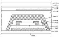
在一种实施例中,请参阅图2和图3,图2是图1所示的显示面板的栅极驱动走线区的第一种局部截面结构示意图,图3是图1所示的显示面板的显示区的第一种局部截面结构示意图。In an embodiment, please refer to FIG. 2 and FIG. 3 , FIG. 2 is a schematic diagram of a first partial cross-sectional structure of the gate driving wiring area of the display panel shown in FIG. 1 , and FIG. 3 is the display shown in FIG. 1 . A schematic diagram of the first partial cross-sectional structure of the display area of the panel.
所述显示面板包括覆盖所述显示区10和所述栅极驱动走线区20的衬底基板101,所述衬底基板101可以是玻璃等硬质基板,也可以是聚酰亚胺等柔性基板。The display panel includes a
所述显示面板包括设置于所述衬底基板101上的第一金属层102,所述第一金属层102覆盖所述显示面板的显示区10和栅极驱动走线区20。所述第一金属层102上设置有金属走线,比如位于所述栅极驱动走线区20内的栅极和栅极线。The display panel includes a
所述显示面板包括覆盖所述第一金属层102的第一绝缘层103,所述第一绝缘层103覆盖所述显示面板的显示区10和栅极驱动走线区20。所述第一绝缘层103包括无机绝缘材料。所述第一绝缘层103可以是栅极绝缘层。The display panel includes a
所述显示面板包括设置于所述第一绝缘层103上的半导体层104,所述半导体层104覆盖所述显示面板的显示区10和栅极驱动走线区20。所述半导体层104内设置有半导体材料,所述半导体材料用于形成薄膜晶体管的有源层。The display panel includes a
所述显示面板还包括设置于所述半导体层104上的第二金属层105,所述第二金属层105覆盖所述显示面板的显示区10和栅极驱动走线区20。所述第二金属层105的局部区域位于所述第一绝缘层103上,所述第二金属层105与所述第一金属层102通过所述第一绝缘层103保持电性绝缘。所述第二金属层105上设置有金属走线,所述金属走线包括用于构成薄膜晶体管的源极线和漏极线。The display panel further includes a
所述显示面板还包括覆盖所述第二金属层105的第二绝缘层106,所述第二绝缘层106覆盖所述显示面板的显示区10和栅极驱动走线区20。所述第二绝缘层106还可以进一步覆盖所述第一绝缘层103和所述半导体层104。所述第二绝缘层106包括无机绝缘材料。The display panel further includes a second insulating
所述显示面板还包括位于所述第二绝缘层106上的色阻层107,所述色阻层107覆盖所述显示面板的显示区10和栅极驱动走线区20。所述色阻层107包括多个色阻。The display panel further includes a color resist
在所述栅极驱动走线区20内,所述色阻层107内的色阻至少覆盖所述第二金属层105所在的区域。由于所述第二金属层105位于所述第一金属层102和第一绝缘层103的上层,因此,覆盖所述第二金属层105的色阻也自然覆盖所述第一金属层102和第一绝缘层103;并且所述色阻层107由于位于所述第二绝缘层106的上层,其必然会对所述第二绝缘层106形成覆盖。因此,本实施例可以利用所述色阻层107实现对所述第二金属层105以及所述第二金属层105附近的绝缘膜层的保护。In the gate driving
进一步地,位于所述栅极驱动走线区20的色阻可以是蓝色阻、绿色阻和红色阻中的至少一种,优选为蓝色阻。当所述栅极驱动走线区20的色阻设置为蓝色阻时,在实现利用色阻对第二金属层105及第二金属层105附近的膜层进行保护的同时,利用透过蓝色阻的光线偏暗的特点,达到显示面板在栅极驱动走线区20内低透光或不透光的效果,提升显示面板的显示品质。Further, the color resistor located in the gate driving
本实施例通过在所述栅极驱动走线区20内设置覆盖所述第二金属层105的色阻,增强了对第二金属层105及第二金属层105的附近膜层的保护,防止显示面板的刻蚀等制程对覆盖所述第二金属层105的绝缘膜层以及第一金属层102与第二金属层105之间的绝缘膜层产生刻蚀破坏效果,并导致第二金属层105暴露以及第一金属层102与第二金属层105短路。因此,本实施例有利于提升显示面板的制程良率。In this embodiment, by arranging a color resistance covering the
在所述显示区10内,所述色阻层107包括阵列排布的多个色阻块,每个所述色阻块对应所述显示面板的一个像素单元设置。位于所述显示区10内的色阻包括红色阻、绿色阻和蓝色阻,所述红色阻、所述绿色阻和所述蓝色阻交替排列,所述红色阻对应所述显示面板的红像素单元,所述绿色阻对应所述显示面板的绿像素单元,所述蓝色阻对应所述显示面板的蓝像素单元。位于所述显示区10的色阻用于对所述显示面板的出光进行过滤,从而实现彩色显示。In the
此外,位于所述显示区10的色阻和位于所述栅极驱动走线区20的色阻在材料和制作工艺上保持一致,因此,在制作显示区10内的色阻时可以同步完成栅极驱动走线区20内色阻的制作。因此,本实施例提供的在栅极驱动走线区20制作色阻结构的设计不会导致显示面板制程工艺的复杂化。In addition, the color resists located in the
所述显示面板还包括设置于所述色阻层107上的光阻层108,所述光阻层108覆盖所述显示面板的显示区10和栅极驱动走线区20。所述光阻层108用于对所述色阻层107及所述色阻层107以下的金属层和绝缘性膜层提供进一步的保护,降低出现刻蚀损伤的风险。The display panel further includes a
所述显示面板还包括设置于所述光阻层108上的像素电极109,所述像素电极109覆盖所述显示区10,并且所述像素电极109至少覆盖部分所述栅极驱动走线区20。位于所述显示区10内的像素电极109通过所述光阻层108、所述色阻层107和所述第二绝缘层106上的过孔,与所述第二金属层105电性连接。所述像素电极109对应显示面板的像素单元设置,所述像素电极109接收由所述第二金属层105传输的数据信号以控制各个像素单元的显示。The display panel further includes a
所述显示面板还包括设置于所述像素电极109上的液晶层111,且所述液晶层111对应所述显示区10设置。所述栅极驱动走线区20在对应所述液晶层111的膜层设置有封框胶110。所述液晶层111内设置有液晶,所述液晶用于调整所述显示面板的显示灰阶。所述封框胶110用于对所述液晶层111的侧边进行封装。The display panel further includes a
所述显示面板还包括设置于所述液晶层111和所述封框胶110上的公共电极112,所述公共电极112覆盖所述显示面板的显示区10和栅极驱动走线区20。所述公共电极112电性连接至所述公共走线区30。所述公共电极112用于提供公共电压,以驱动所述液晶层111内的液晶产生偏转。The display panel further includes a
所述显示面板还包括位于所述公共电极112上的上基板113,所述上基板113覆盖所述显示面板的显示区10和栅极驱动走线区20。The display panel further includes an
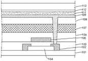
在一种实施例中,请参阅图4,图4是图1所示的显示面板的栅极驱动走线区的第二种局部截面结构示意图。其中,与图4对应的显示区的截面结构和图3所示的显示区的截面结构相同。In an embodiment, please refer to FIG. 4 . FIG. 4 is a schematic diagram of a second partial cross-sectional structure of the gate driving wiring area of the display panel shown in FIG. 1 . The cross-sectional structure of the display area corresponding to FIG. 4 is the same as the cross-sectional structure of the display area shown in FIG. 3 .
图4所示的栅极驱动走线区20的截面结构与图2所示的栅极驱动走线区20的截面结构相似,其不同之处仅在于以下方面:The cross-sectional structure of the gate driving
所述第一绝缘层103沿所述第一金属层102的布置位置覆盖所述第一金属层102的全部外露表面。所述第二绝缘层106沿所述第二金属层105的布置位置覆盖所述第二金属层105的全部外露表面。所述色阻层107对所述第一绝缘层103和所述第二绝缘层106的全部外露表面形成包围式覆盖,从而对所述第一绝缘层103和所述第二绝缘层106形成全面保护,防止显示面板的刻蚀等制程对所述第一绝缘层103和所述第二绝缘层106造成破坏。The first insulating
本实施例通过在所述栅极驱动走线区20内设置色阻,对第二金属层105及第二金属层105的附近膜层进行保护,防止显示面板的刻蚀等制程对覆盖所述第二金属层105的绝缘膜层以及第一金属层102与第二金属层105之间的绝缘膜层产生刻蚀破坏效果,进而防止第二金属层105暴露以及第一金属层102与第二金属层105短路,有利于提升显示面板的制程良率;且覆盖第二金属层105的色阻与显示区10的色阻相同,可以通过同一制程制作,因此在栅极驱动走线区20增加色阻结构不会导致显示面板制程工艺的复杂化。In this embodiment, by arranging a color resist in the gate driving
在一种实施例中,请参阅图5和图6,图5是图1所示的显示面板的栅极驱动走线区的第三种局部截面结构示意图,图6是图1所示的显示面板的显示区的第二种局部截面结构示意图。其中,图5所示的栅极驱动走线区的显示面板结构与图2所示的栅极驱动走线区的显示面板结构相同或相似,图6所示的显示区的显示面板结构与图3所示的显示区的显示面板结构相同或相似,下面对图5和图6所示的显示面板结构进行说明,其中未详述之处,请参阅上述实施例的记载。In one embodiment, please refer to FIG. 5 and FIG. 6 , FIG. 5 is a schematic diagram of a third partial cross-sectional structure of the gate driving wiring area of the display panel shown in FIG. 1 , and FIG. 6 is the display shown in FIG. 1 . A schematic diagram of a second partial cross-sectional structure of the display area of the panel. The structure of the display panel in the gate driving wiring area shown in FIG. 5 is the same as or similar to the display panel structure in the gate driving wiring area shown in FIG. 2 , and the structure of the display panel in the display area shown in FIG. The structure of the display panel in the display area shown in 3 is the same or similar. The structure of the display panel shown in FIG. 5 and FIG. 6 will be described below.
所述显示面板包括覆盖所述显示区10和所述栅极驱动走线区20的衬底基板101。所述衬底基板101上设置有第一金属层102和半导体层104,所述第一金属层102和所述半导体层104均覆盖所述显示面板的显示区10和栅极驱动走线区20。所述半导体层104内设置有半导体材料,所述半导体材料用于形成薄膜晶体管的有源层。所述第一金属层102上设置有金属走线,所述金属走线包括用于构成薄膜晶体管的源极和漏极。The display panel includes a
所述显示面板包括覆盖所述第一金属层102和所述半导体层104的第一绝缘层103,所述第一绝缘层103覆盖所述显示面板的显示区10和栅极驱动走线区20。所述第一绝缘层103包括无机绝缘材料。所述第一绝缘层103可以是栅极绝缘层。The display panel includes a first insulating
所述显示面板还包括设置于所述第一绝缘层103上的第二金属层105,所述第二金属层105覆盖所述显示面板的显示区10和栅极驱动走线区20。所述第二金属层105上设置有金属走线,所述金属走线包括用于构成薄膜晶体管的栅极。The display panel further includes a
所述显示面板还包括覆盖所述第二金属层105的第二绝缘层106,所述第二绝缘层106覆盖所述显示面板的显示区10和栅极驱动走线区20。The display panel further includes a second insulating
所述显示面板还包括位于所述第二绝缘层106上的色阻层107,所述色阻层107覆盖所述显示面板的显示区10和栅极驱动走线区20。所述色阻层107包括多个色阻。The display panel further includes a color resist
在所述栅极驱动走线区20内,所述色阻层107内的色阻至少覆盖所述第二金属层105所在的区域。由于所述第二金属层105位于所述第一金属层102和第一绝缘层103的上层,因此,覆盖所述第二金属层105的色阻也自然覆盖所述第一金属层102和第一绝缘层103;并且所述色阻层107由于位于所述第二绝缘层106的上层,其必然会对所述第二绝缘层106形成覆盖。因此,本实施例可以利用所述色阻层107实现对所述第二金属层105以及所述第二金属层105附近的绝缘膜层的保护。In the gate driving
进一步地,位于所述栅极驱动走线区20的色阻可以是蓝色阻、绿色阻和红色阻中的至少一种,优选为蓝色阻。当所述栅极驱动走线区20的色阻设置为蓝色阻时,在实现利用色阻对第二金属层105及第二金属层105附近的膜层进行保护的同时,利用透过蓝色阻的光线偏暗的特点,达到显示面板在栅极驱动走线区20内低透光或不透光的效果,提升显示面板的显示品质。Further, the color resistor located in the gate driving
本实施例通过在所述栅极驱动走线区20内设置覆盖所述第二金属层105的色阻,增强了对第二金属层105及第二金属层105的附近膜层的保护,防止显示面板的刻蚀等制程对覆盖所述第二金属层105的绝缘膜层以及第一金属层102与第二金属层105之间的绝缘膜层产生刻蚀破坏效果,并导致第二金属层105暴露以及第一金属层102与第二金属层105短路。因此,本实施例有利于提升显示面板的制程良率。In this embodiment, by arranging a color resistance covering the
在所述显示区10内,所述色阻层107包括阵列排布的多个色阻块,每个所述色阻块对应所述显示面板的一个像素单元设置。位于所述显示区10内的色阻包括红色阻、绿色阻和蓝色阻,所述红色阻、所述绿色阻和所述蓝色阻交替排列,所述红色阻对应所述显示面板的红像素单元,所述绿色阻对应所述显示面板的绿像素单元,所述蓝色阻对应所述显示面板的蓝像素单元。位于所述显示区10的色阻用于对所述显示面板的出光进行过滤,从而实现彩色显示。In the
此外,位于所述显示区10的色阻和位于所述栅极驱动走线区20的色阻在材料和制作工艺上保持一致,因此,在制作显示区10内的色阻时可以同步完成栅极驱动走线区20内色阻的制作。因此,本实施例提供的在栅极驱动走线区20制作色阻结构的设计不会导致显示面板制程工艺的复杂化。In addition, the color resists located in the
所述显示面板还包括设置于所述色阻层107上的光阻层108,所述光阻层108覆盖所述显示面板的显示区10和栅极驱动走线区20。The display panel further includes a
所述显示面板还包括设置于所述光阻层108上的像素电极109,所述像素电极109覆盖所述显示区10,并且所述像素电极109至少覆盖部分所述栅极驱动走线区20。位于所述显示区10内的像素电极109通过所述光阻层108、所述色阻层107、所述第二绝缘层106和所述第一绝缘层103上的过孔,与所述第一金属层102电性连接。所述像素电极109对应显示面板的像素单元设置,所述像素电极109接收由所述第一金属层102传输的数据信号以控制各个像素单元的显示。The display panel further includes a
所述显示面板还包括设置于所述像素电极109上的液晶层111,且所述液晶层111对应所述显示区10设置。所述栅极驱动走线区20在对应所述液晶层111的膜层设置有封框胶110。所述液晶层111内设置有液晶,所述液晶用于调整所述显示面板的显示灰阶。所述封框胶110用于对所述液晶层111的侧边进行封装。The display panel further includes a
所述显示面板还包括设置于所述液晶层111和所述封框胶110上的公共电极112,所述公共电极112覆盖所述显示面板的显示区10和栅极驱动走线区20。所述公共电极112电性连接至所述公共走线区30。所述公共电极112用于提供公共电压,以驱动所述液晶层111内的液晶产生偏转。The display panel further includes a
所述显示面板还包括位于所述公共电极112上的上基板113,所述上基板113覆盖所述显示面板的显示区10和栅极驱动走线区20。The display panel further includes an
可选地,请参阅图5,所述第一绝缘层103还可以沿所述第一金属层102的布置位置覆盖所述第一金属层102的全部外露表面。所述第二绝缘层106还可以沿所述第二金属层105的布置位置覆盖所述第二金属层105的全部外露表面。所述色阻层107对所述第一绝缘层103和所述第二绝缘层106的全部外露表面形成包围式覆盖,从而对所述第一绝缘层103和所述第二绝缘层106形成全面保护。Optionally, referring to FIG. 5 , the first insulating
综上所述,本申请实施例提供的显示面板,通过在栅极驱动走线区内设置色阻,对第二金属层及第二金属层的附近膜层进行保护,防止显示面板的刻蚀等制程对覆盖所述第二金属层的绝缘膜层以及第一金属层与第二金属层之间的绝缘膜层产生刻蚀破坏效果,进而防止第二金属层暴露以及第一金属层与第二金属层短路,有利于提升显示面板的制程良率;且覆盖第二金属层的色阻与显示区的色阻相同,可以通过同一制程制作,因此在栅极驱动走线区增加色阻结构不会导致显示面板制程工艺的复杂化。To sum up, in the display panel provided by the embodiments of the present application, the second metal layer and the film layers near the second metal layer are protected by arranging color resists in the gate driving wiring area to prevent the display panel from being etched. Etc. process produces an etching damage effect on the insulating film covering the second metal layer and the insulating film between the first metal layer and the second metal layer, thereby preventing the second metal layer from being exposed and the first metal layer and the second metal layer from being exposed. The two metal layers are short-circuited, which is beneficial to improve the process yield of the display panel; and the color resistance covering the second metal layer is the same as the color resistance of the display area, and can be fabricated through the same process, so a color resistance structure is added in the gate driving wiring area. It will not lead to the complexity of the display panel manufacturing process.
本申请实施例还提供一种显示装置,所述显示装置包括本申请实施例提供的显示面板。所述显示装置可以是显示器、手机、平板电脑、笔记本电脑、导航仪、电视机等具有显示功能的器件。Embodiments of the present application further provide a display device, where the display device includes the display panel provided by the embodiments of the present application. The display device may be a display device, a mobile phone, a tablet computer, a notebook computer, a navigator, a television, or the like, which has a display function.
需要说明的是,虽然本申请以具体实施例揭露如上,但上述实施例并非用以限制本申请,本领域的普通技术人员,在不脱离本申请的精神和范围内,均可作各种更动与润饰,因此本申请的保护范围以权利要求界定的范围为准。It should be noted that although the present application discloses the above with specific embodiments, the above-mentioned embodiments are not intended to limit the present application. Those of ordinary skill in the art can make various modifications without departing from the spirit and scope of the present application. Therefore, the scope of protection of this application is subject to the scope defined by the claims.
Claims (8)
Translated fromChinesePriority Applications (5)
| Application Number | Priority Date | Filing Date | Title |
|---|---|---|---|
| CN202110392451.4ACN113138487B (en) | 2021-04-13 | 2021-04-13 | Display panel and display device |
| JP2021526344AJP7397556B2 (en) | 2021-04-13 | 2021-05-10 | Display panel and display device |
| PCT/CN2021/092579WO2022217678A1 (en) | 2021-04-13 | 2021-05-10 | Display panel and display apparatus |
| US17/309,482US12066729B2 (en) | 2021-04-13 | 2021-05-10 | Display panel and display device |
| EP21731036.6AEP4325283A4 (en) | 2021-04-13 | 2021-05-10 | Display panel and display apparatus |
Applications Claiming Priority (1)
| Application Number | Priority Date | Filing Date | Title |
|---|---|---|---|
| CN202110392451.4ACN113138487B (en) | 2021-04-13 | 2021-04-13 | Display panel and display device |
Publications (2)
| Publication Number | Publication Date |
|---|---|
| CN113138487A CN113138487A (en) | 2021-07-20 |
| CN113138487Btrue CN113138487B (en) | 2022-08-05 |
Family
ID=76811224
Family Applications (1)
| Application Number | Title | Priority Date | Filing Date |
|---|---|---|---|
| CN202110392451.4AActiveCN113138487B (en) | 2021-04-13 | 2021-04-13 | Display panel and display device |
Country Status (5)
| Country | Link |
|---|---|
| US (1) | US12066729B2 (en) |
| EP (1) | EP4325283A4 (en) |
| JP (1) | JP7397556B2 (en) |
| CN (1) | CN113138487B (en) |
| WO (1) | WO2022217678A1 (en) |
Families Citing this family (1)
| Publication number | Priority date | Publication date | Assignee | Title |
|---|---|---|---|---|
| CN114428427B (en)* | 2022-01-27 | 2023-10-03 | Tcl华星光电技术有限公司 | Display panel and display device |
Citations (3)
| Publication number | Priority date | Publication date | Assignee | Title |
|---|---|---|---|---|
| JP2003228082A (en)* | 2002-02-01 | 2003-08-15 | Acer Display Technology Inc | Method for manufacturing thin film transistor liquid crystal display device |
| CN101673017A (en)* | 2009-10-28 | 2010-03-17 | 友达光电股份有限公司 | Active component array substrate and manufacturing method thereof |
| CN106681071A (en)* | 2016-12-29 | 2017-05-17 | 惠科股份有限公司 | Liquid crystal display panel and preparation method thereof |
Family Cites Families (20)
| Publication number | Priority date | Publication date | Assignee | Title |
|---|---|---|---|---|
| JP3277732B2 (en) | 1994-11-24 | 2002-04-22 | ソニー株式会社 | Color display |
| JP2001175198A (en)* | 1999-12-14 | 2001-06-29 | Semiconductor Energy Lab Co Ltd | Semiconductor device and manufacturing method thereof |
| TWI253538B (en)* | 2000-09-30 | 2006-04-21 | Au Optronics Corp | Thin film transistor flat display and its manufacturing method |
| JP2003202589A (en) | 2001-12-28 | 2003-07-18 | Fujitsu Display Technologies Corp | Liquid crystal display device and method of manufacturing the same |
| JP5110803B2 (en)* | 2006-03-17 | 2012-12-26 | キヤノン株式会社 | FIELD EFFECT TRANSISTOR USING OXIDE FILM FOR CHANNEL AND METHOD FOR MANUFACTURING THE SAME |
| KR101294260B1 (en)* | 2006-08-18 | 2013-08-06 | 삼성디스플레이 주식회사 | Organic light emitting diode display and method for manufacturing the same |
| JP2008205333A (en)* | 2007-02-22 | 2008-09-04 | Toshiba Matsushita Display Technology Co Ltd | Thin film transistor and method for manufacturing the same |
| KR101910451B1 (en)* | 2008-07-10 | 2018-10-22 | 가부시키가이샤 한도오따이 에네루기 켄큐쇼 | Light-emitting device and electronic device using the same |
| KR101458914B1 (en)* | 2008-08-20 | 2014-11-07 | 삼성디스플레이 주식회사 | Liquid Crystal Display |
| CN101692327A (en) | 2009-11-02 | 2010-04-07 | 友达光电股份有限公司 | Flat display device with control circuit protection function |
| US8952379B2 (en)* | 2011-09-16 | 2015-02-10 | Semiconductor Energy Laboratory Co., Ltd. | Semiconductor device |
| CN104393003A (en)* | 2014-10-31 | 2015-03-04 | 深圳市华星光电技术有限公司 | TFT substrate and manufacturing method thereof |
| TW201631367A (en)* | 2015-02-25 | 2016-09-01 | 友達光電股份有限公司 | Display panel and its making method |
| CN106547127B (en)* | 2017-01-16 | 2019-10-25 | 上海天马微电子有限公司 | Array substrate, liquid crystal display panel and display device |
| CN107908047B (en) | 2017-12-21 | 2020-09-04 | 惠科股份有限公司 | Display panel and display device |
| KR102477605B1 (en)* | 2018-01-23 | 2022-12-14 | 삼성디스플레이 주식회사 | Display apparatus and method of manufacturing the same |
| CN108761941B (en)* | 2018-05-31 | 2021-04-20 | Tcl华星光电技术有限公司 | COA type liquid crystal display panel structure and manufacturing method of COA type liquid crystal display panel |
| CN109887968A (en)* | 2019-02-25 | 2019-06-14 | 深圳市华星光电半导体显示技术有限公司 | A display panel and method of making the same |
| CN109976049A (en)* | 2019-04-08 | 2019-07-05 | 深圳市华星光电半导体显示技术有限公司 | Display panel and preparation method thereof |
| CN112068372A (en)* | 2020-09-10 | 2020-12-11 | 深圳市华星光电半导体显示技术有限公司 | Array substrate and display panel |
- 2021
- 2021-04-13CNCN202110392451.4Apatent/CN113138487B/enactiveActive
- 2021-05-10JPJP2021526344Apatent/JP7397556B2/enactiveActive
- 2021-05-10USUS17/309,482patent/US12066729B2/enactiveActive
- 2021-05-10EPEP21731036.6Apatent/EP4325283A4/enactivePending
- 2021-05-10WOPCT/CN2021/092579patent/WO2022217678A1/ennot_activeCeased
Patent Citations (3)
| Publication number | Priority date | Publication date | Assignee | Title |
|---|---|---|---|---|
| JP2003228082A (en)* | 2002-02-01 | 2003-08-15 | Acer Display Technology Inc | Method for manufacturing thin film transistor liquid crystal display device |
| CN101673017A (en)* | 2009-10-28 | 2010-03-17 | 友达光电股份有限公司 | Active component array substrate and manufacturing method thereof |
| CN106681071A (en)* | 2016-12-29 | 2017-05-17 | 惠科股份有限公司 | Liquid crystal display panel and preparation method thereof |
Also Published As
| Publication number | Publication date |
|---|---|
| WO2022217678A1 (en) | 2022-10-20 |
| JP2023524181A (en) | 2023-06-09 |
| US12066729B2 (en) | 2024-08-20 |
| EP4325283A4 (en) | 2025-02-05 |
| EP4325283A1 (en) | 2024-02-21 |
| US20240053645A1 (en) | 2024-02-15 |
| JP7397556B2 (en) | 2023-12-13 |
| CN113138487A (en) | 2021-07-20 |
Similar Documents
| Publication | Publication Date | Title |
|---|---|---|
| US9568795B2 (en) | Liquid crystal display device | |
| JP4643738B2 (en) | COT-structured liquid crystal display device for preventing light leakage from outer portion of pixel region and manufacturing method thereof | |
| US9240149B2 (en) | Liquid crystal display device and method of fabricating the same | |
| US9274379B2 (en) | Liquid crystal display device | |
| JP5392975B2 (en) | Liquid crystal display device and manufacturing method thereof | |
| KR101791578B1 (en) | Liquid crystal display | |
| JP2002277889A (en) | Active matrix liquid crystal display | |
| KR20030094599A (en) | A thin film transistor array panel | |
| US9164334B2 (en) | Display device and method of manufacturing same | |
| KR20100022762A (en) | Liquid crystal display | |
| US11586088B2 (en) | Display substrate, display panel and display apparatus | |
| US6917408B2 (en) | Display panel | |
| KR101621559B1 (en) | Liquid crystal display device | |
| JP3216379B2 (en) | Liquid crystal display | |
| WO2017024708A1 (en) | Display substrate and manufacturing method therefor, and display device | |
| KR101866263B1 (en) | Liquid crystal display device | |
| US20120319144A1 (en) | Display panel and display device | |
| JP2005173613A (en) | Thin film transistor display panel | |
| KR20140117925A (en) | Liquid crystal display device having minimized bezzel | |
| CN113138487B (en) | Display panel and display device | |
| CN103293751B (en) | A kind of color membrane substrates of liquid crystal display and manufacture method thereof | |
| JPH11258629A (en) | Manufacturing method of liquid crystal display device | |
| JP2004004526A (en) | Liquid crystal display | |
| JP2009020421A (en) | Liquid crystal device and electronic apparatus | |
| US12057456B2 (en) | Array substrate and display panel |
Legal Events
| Date | Code | Title | Description |
|---|---|---|---|
| PB01 | Publication | ||
| PB01 | Publication | ||
| SE01 | Entry into force of request for substantive examination | ||
| SE01 | Entry into force of request for substantive examination | ||
| GR01 | Patent grant | ||
| GR01 | Patent grant |