CN113130794A - Quantum dot light-emitting diode and preparation method thereof - Google Patents
Quantum dot light-emitting diode and preparation method thereofDownload PDFInfo
- Publication number
- CN113130794A CN113130794ACN201911425210.4ACN201911425210ACN113130794ACN 113130794 ACN113130794 ACN 113130794ACN 201911425210 ACN201911425210 ACN 201911425210ACN 113130794 ACN113130794 ACN 113130794A
- Authority
- CN
- China
- Prior art keywords
- dot light
- quantum dot
- emitting layer
- layer
- emitting
- Prior art date
- Legal status (The legal status is an assumption and is not a legal conclusion. Google has not performed a legal analysis and makes no representation as to the accuracy of the status listed.)
- Granted
Links
- 239000002096quantum dotSubstances0.000titleclaimsabstractdescription323
- 238000002360preparation methodMethods0.000titleabstractdescription12
- 125000006850spacer groupChemical group0.000claimsabstractdescription91
- 239000002245particleSubstances0.000claimsdescription51
- 238000000034methodMethods0.000claimsdescription26
- 239000000463materialSubstances0.000claimsdescription21
- 238000004519manufacturing processMethods0.000claimsdescription6
- 238000002347injectionMethods0.000abstractdescription18
- 239000007924injectionSubstances0.000abstractdescription18
- 238000002866fluorescence resonance energy transferMethods0.000abstractdescription13
- 238000012546transferMethods0.000abstractdescription8
- 230000004888barrier functionEffects0.000abstractdescription5
- 230000005525hole transportEffects0.000description17
- IJGRMHOSHXDMSA-UHFFFAOYSA-NAtomic nitrogenChemical compoundN#NIJGRMHOSHXDMSA-UHFFFAOYSA-N0.000description8
- XLOMVQKBTHCTTD-UHFFFAOYSA-NZinc monoxideChemical compound[Zn]=OXLOMVQKBTHCTTD-UHFFFAOYSA-N0.000description8
- 229910052757nitrogenInorganic materials0.000description8
- XOLBLPGZBRYERU-UHFFFAOYSA-Ntin dioxideChemical compoundO=[Sn]=OXOLBLPGZBRYERU-UHFFFAOYSA-N0.000description8
- 229910001887tin oxideInorganic materials0.000description8
- 239000011701zincSubstances0.000description7
- 239000010931goldSubstances0.000description6
- 238000004020luminiscence typeMethods0.000description6
- 230000006798recombinationEffects0.000description6
- 238000005215recombinationMethods0.000description6
- 238000004528spin coatingMethods0.000description6
- 238000000576coating methodMethods0.000description5
- 238000005401electroluminescenceMethods0.000description5
- -1poly(3,4-ethylenedioxythiophene)Polymers0.000description5
- 239000000758substrateSubstances0.000description5
- 229920000144PEDOT:PSSPolymers0.000description4
- BQCADISMDOOEFD-UHFFFAOYSA-NSilverChemical compound[Ag]BQCADISMDOOEFD-UHFFFAOYSA-N0.000description4
- 229910052782aluminiumInorganic materials0.000description4
- 238000000137annealingMethods0.000description4
- 238000012512characterization methodMethods0.000description4
- 229910052737goldInorganic materials0.000description4
- 239000011787zinc oxideSubstances0.000description4
- YBNMDCCMCLUHBL-UHFFFAOYSA-N(2,5-dioxopyrrolidin-1-yl) 4-pyren-1-ylbutanoateChemical compoundC=1C=C(C2=C34)C=CC3=CC=CC4=CC=C2C=1CCCC(=O)ON1C(=O)CCC1=OYBNMDCCMCLUHBL-UHFFFAOYSA-N0.000description3
- 230000008901benefitEffects0.000description3
- UHYPYGJEEGLRJD-UHFFFAOYSA-Ncadmium(2+);selenium(2-)Chemical compound[Se-2].[Cd+2]UHYPYGJEEGLRJD-UHFFFAOYSA-N0.000description3
- 238000000151depositionMethods0.000description3
- 229920003227poly(N-vinyl carbazole)Polymers0.000description3
- 229910052717sulfurInorganic materials0.000description3
- 229910052725zincInorganic materials0.000description3
- 238000002441X-ray diffractionMethods0.000description2
- XAGFODPZIPBFFR-UHFFFAOYSA-NaluminiumChemical compound[Al]XAGFODPZIPBFFR-UHFFFAOYSA-N0.000description2
- 230000008859changeEffects0.000description2
- 239000011248coating agentSubstances0.000description2
- 238000010586diagramMethods0.000description2
- ZUOUZKKEUPVFJK-UHFFFAOYSA-NdiphenylChemical compoundC1=CC=CC=C1C1=CC=CC=C1ZUOUZKKEUPVFJK-UHFFFAOYSA-N0.000description2
- DMBHHRLKUKUOEG-UHFFFAOYSA-NdiphenylamineChemical compoundC=1C=CC=CC=1NC1=CC=CC=C1DMBHHRLKUKUOEG-UHFFFAOYSA-N0.000description2
- 238000009826distributionMethods0.000description2
- 238000005538encapsulationMethods0.000description2
- 238000005516engineering processMethods0.000description2
- PCHJSUWPFVWCPO-UHFFFAOYSA-NgoldChemical compound[Au]PCHJSUWPFVWCPO-UHFFFAOYSA-N0.000description2
- 150000002500ionsChemical class0.000description2
- 238000001755magnetron sputter depositionMethods0.000description2
- 239000002086nanomaterialSubstances0.000description2
- 239000012299nitrogen atmosphereSubstances0.000description2
- 238000000053physical methodMethods0.000description2
- 229910052709silverInorganic materials0.000description2
- 239000004332silverSubstances0.000description2
- 239000000243solutionSubstances0.000description2
- 239000000126substanceSubstances0.000description2
- 238000010998test methodMethods0.000description2
- 238000012360testing methodMethods0.000description2
- 230000009466transformationEffects0.000description2
- 238000000844transformationMethods0.000description2
- 238000004627transmission electron microscopyMethods0.000description2
- LGDCSNDMFFFSHY-UHFFFAOYSA-N4-butyl-n,n-diphenylanilinePolymersC1=CC(CCCC)=CC=C1N(C=1C=CC=CC=1)C1=CC=CC=C1LGDCSNDMFFFSHY-UHFFFAOYSA-N0.000description1
- AWXGSYPUMWKTBR-UHFFFAOYSA-N4-carbazol-9-yl-n,n-bis(4-carbazol-9-ylphenyl)anilineChemical compoundC12=CC=CC=C2C2=CC=CC=C2N1C1=CC=C(N(C=2C=CC(=CC=2)N2C3=CC=CC=C3C3=CC=CC=C32)C=2C=CC(=CC=2)N2C3=CC=CC=C3C3=CC=CC=C32)C=C1AWXGSYPUMWKTBR-UHFFFAOYSA-N0.000description1
- OKTJSMMVPCPJKN-UHFFFAOYSA-NCarbonChemical compound[C]OKTJSMMVPCPJKN-UHFFFAOYSA-N0.000description1
- 229910004613CdTeInorganic materials0.000description1
- 229910019923CrOxInorganic materials0.000description1
- QPLDLSVMHZLSFG-UHFFFAOYSA-NCuOInorganic materials[Cu]=OQPLDLSVMHZLSFG-UHFFFAOYSA-N0.000description1
- 101000837344Homo sapiens T-cell leukemia translocation-altered gene proteinProteins0.000description1
- 229910015711MoOxInorganic materials0.000description1
- 229910003185MoSxInorganic materials0.000description1
- 229910005855NiOxInorganic materials0.000description1
- 229910006404SnO 2Inorganic materials0.000description1
- 102100028692T-cell leukemia translocation-altered gene proteinHuman genes0.000description1
- 229910010413TiO 2Inorganic materials0.000description1
- 239000007983Tris bufferSubstances0.000description1
- 229910007717ZnSnOInorganic materials0.000description1
- 238000010521absorption reactionMethods0.000description1
- QVGXLLKOCUKJST-UHFFFAOYSA-Natomic oxygenChemical compound[O]QVGXLLKOCUKJST-UHFFFAOYSA-N0.000description1
- 230000009286beneficial effectEffects0.000description1
- 235000010290biphenylNutrition0.000description1
- 239000004305biphenylSubstances0.000description1
- 150000001720carbohydratesChemical class0.000description1
- 238000005266castingMethods0.000description1
- 238000006243chemical reactionMethods0.000description1
- 238000005229chemical vapour depositionMethods0.000description1
- 238000000975co-precipitationMethods0.000description1
- 229910052802copperInorganic materials0.000description1
- 230000008878couplingEffects0.000description1
- 238000010168coupling processMethods0.000description1
- 238000005859coupling reactionMethods0.000description1
- 230000007812deficiencyEffects0.000description1
- 238000011161developmentMethods0.000description1
- 230000000694effectsEffects0.000description1
- 238000005566electron beam evaporationMethods0.000description1
- 238000001704evaporationMethods0.000description1
- 239000011521glassSubstances0.000description1
- 229910021389grapheneInorganic materials0.000description1
- 238000007654immersionMethods0.000description1
- 229910010272inorganic materialInorganic materials0.000description1
- 239000011147inorganic materialSubstances0.000description1
- JKQOBWVOAYFWKG-UHFFFAOYSA-Nmolybdenum trioxideInorganic materialsO=[Mo](=O)=OJKQOBWVOAYFWKG-UHFFFAOYSA-N0.000description1
- 238000005457optimizationMethods0.000description1
- 239000011368organic materialSubstances0.000description1
- 230000003647oxidationEffects0.000description1
- 238000007254oxidation reactionMethods0.000description1
- 229910052760oxygenInorganic materials0.000description1
- 239000001301oxygenSubstances0.000description1
- ATGUVEKSASEFFO-UHFFFAOYSA-Np-aminodiphenylamineChemical compoundC1=CC(N)=CC=C1NC1=CC=CC=C1ATGUVEKSASEFFO-UHFFFAOYSA-N0.000description1
- 238000004806packaging method and processMethods0.000description1
- 238000012858packaging processMethods0.000description1
- 238000005240physical vapour depositionMethods0.000description1
- 238000007747platingMethods0.000description1
- 229920000172poly(styrenesulfonic acid)Polymers0.000description1
- 238000007639printingMethods0.000description1
- 230000008569processEffects0.000description1
- 238000004549pulsed laser depositionMethods0.000description1
- 230000005855radiationEffects0.000description1
- 238000011160researchMethods0.000description1
- 230000004044responseEffects0.000description1
- SBIBMFFZSBJNJF-UHFFFAOYSA-Nselenium;zincChemical compound[Se]=[Zn]SBIBMFFZSBJNJF-UHFFFAOYSA-N0.000description1
- 239000004065semiconductorSubstances0.000description1
- 238000001179sorption measurementMethods0.000description1
- 230000003595spectral effectEffects0.000description1
- 238000001228spectrumMethods0.000description1
- 238000005507sprayingMethods0.000description1
- 238000004544sputter depositionMethods0.000description1
- 238000002207thermal evaporationMethods0.000description1
- 239000010409thin filmSubstances0.000description1
- ODHXBMXNKOYIBV-UHFFFAOYSA-NtriphenylamineChemical compoundC1=CC=CC=C1N(C=1C=CC=CC=1)C1=CC=CC=C1ODHXBMXNKOYIBV-UHFFFAOYSA-N0.000description1
- XLYOFNOQVPJJNP-UHFFFAOYSA-NwaterSubstancesOXLYOFNOQVPJJNP-UHFFFAOYSA-N0.000description1
Images


Classifications
- H—ELECTRICITY
- H10—SEMICONDUCTOR DEVICES; ELECTRIC SOLID-STATE DEVICES NOT OTHERWISE PROVIDED FOR
- H10K—ORGANIC ELECTRIC SOLID-STATE DEVICES
- H10K50/00—Organic light-emitting devices
- H—ELECTRICITY
- H10—SEMICONDUCTOR DEVICES; ELECTRIC SOLID-STATE DEVICES NOT OTHERWISE PROVIDED FOR
- H10K—ORGANIC ELECTRIC SOLID-STATE DEVICES
- H10K50/00—Organic light-emitting devices
- H10K50/10—OLEDs or polymer light-emitting diodes [PLED]
- H10K50/11—OLEDs or polymer light-emitting diodes [PLED] characterised by the electroluminescent [EL] layers
- H10K50/115—OLEDs or polymer light-emitting diodes [PLED] characterised by the electroluminescent [EL] layers comprising active inorganic nanostructures, e.g. luminescent quantum dots
- H—ELECTRICITY
- H10—SEMICONDUCTOR DEVICES; ELECTRIC SOLID-STATE DEVICES NOT OTHERWISE PROVIDED FOR
- H10K—ORGANIC ELECTRIC SOLID-STATE DEVICES
- H10K50/00—Organic light-emitting devices
- H10K50/10—OLEDs or polymer light-emitting diodes [PLED]
- H10K50/11—OLEDs or polymer light-emitting diodes [PLED] characterised by the electroluminescent [EL] layers
- H10K50/125—OLEDs or polymer light-emitting diodes [PLED] characterised by the electroluminescent [EL] layers specially adapted for multicolour light emission, e.g. for emitting white light
- H10K50/13—OLEDs or polymer light-emitting diodes [PLED] characterised by the electroluminescent [EL] layers specially adapted for multicolour light emission, e.g. for emitting white light comprising stacked EL layers within one EL unit
- H10K50/131—OLEDs or polymer light-emitting diodes [PLED] characterised by the electroluminescent [EL] layers specially adapted for multicolour light emission, e.g. for emitting white light comprising stacked EL layers within one EL unit with spacer layers between the electroluminescent layers
- H—ELECTRICITY
- H10—SEMICONDUCTOR DEVICES; ELECTRIC SOLID-STATE DEVICES NOT OTHERWISE PROVIDED FOR
- H10K—ORGANIC ELECTRIC SOLID-STATE DEVICES
- H10K71/00—Manufacture or treatment specially adapted for the organic devices covered by this subclass
- H—ELECTRICITY
- H10—SEMICONDUCTOR DEVICES; ELECTRIC SOLID-STATE DEVICES NOT OTHERWISE PROVIDED FOR
- H10K—ORGANIC ELECTRIC SOLID-STATE DEVICES
- H10K71/00—Manufacture or treatment specially adapted for the organic devices covered by this subclass
- H10K71/10—Deposition of organic active material
- H10K71/12—Deposition of organic active material using liquid deposition, e.g. spin coating
Landscapes
- Electroluminescent Light Sources (AREA)
Abstract
Translated fromChinese
Description
Translated fromChinese技术领域technical field
本发明涉及量子点发光二极管技术领域,尤其涉及一种量子点发光二极管及其制备方法。The invention relates to the technical field of quantum dot light-emitting diodes, in particular to a quantum dot light-emitting diode and a preparation method thereof.
背景技术Background technique
量子点电致发光是一种新型的固态照明技术,具备低成本、重量轻、响应速度快、色彩饱和度高等优点,拥有广阔的发展前景,已成为新一代LED照明的重要研究方向之一。Quantum dot electroluminescence is a new type of solid-state lighting technology. It has the advantages of low cost, light weight, fast response speed and high color saturation. It has broad development prospects and has become one of the important research directions of a new generation of LED lighting.
现有量子点发光二极管(QLED)主要结构为阴极、阳极、空穴/电子传输层以及量子点发光层,但其亮度、量子效率以及寿命还未能达到一个理想的数值,主要原因是因为薄膜材料的选择和制备流程的优化还不够完善。The main structures of existing quantum dot light-emitting diodes (QLEDs) are cathode, anode, hole/electron transport layer and quantum dot light-emitting layer, but their brightness, quantum efficiency and lifetime have not yet reached an ideal value, mainly due to the thin film The selection of materials and the optimization of the preparation process are not perfect.
因此,现有技术还有待于改进和发展。Therefore, the existing technology still needs to be improved and developed.
发明内容SUMMARY OF THE INVENTION
鉴于上述现有技术的不足,本发明的目的在于提供一种量子点发光二极管及其制备方法,旨在一定程度解决现有量子点发光二极管亮度、量子效率以及寿命不够理想的问题。In view of the above-mentioned deficiencies of the prior art, the purpose of the present invention is to provide a quantum dot light-emitting diode and a preparation method thereof, aiming at solving the problems of unsatisfactory brightness, quantum efficiency and lifespan of the existing quantum dot light-emitting diode to a certain extent.
本发明的技术方案如下:The technical scheme of the present invention is as follows:
一种量子点发光二极管,其中,包括:阳极、阴极、设置于所述阳极和阴极之间的叠层,所述叠层包括第一量子点发光层、间隔层和第二量子点发光层,所述间隔层设置于所述第一量子点发光层及所述第二量子点发光层之间,所述间隔层包括多个ZnS量子点。A quantum dot light-emitting diode, comprising: an anode, a cathode, and a stack disposed between the anode and the cathode, the stack comprising a first quantum dot light-emitting layer, a spacer layer and a second quantum dot light-emitting layer, The spacer layer is disposed between the first quantum dot light-emitting layer and the second quantum dot light-emitting layer, and the spacer layer includes a plurality of ZnS quantum dots.
一种量子点发光二极管的制备方法,其中,包括步骤:A preparation method of a quantum dot light-emitting diode, comprising the steps of:
提供阳极;provide anodes;
在所述阳极上形成第一量子点发光层;forming a first quantum dot light-emitting layer on the anode;
在所述第一量子点发光层上形成间隔层,所述间隔层包括多个ZnS量子点;;forming a spacer layer on the first quantum dot light-emitting layer, the spacer layer comprising a plurality of ZnS quantum dots;
在所述间隔层上形成第二量子点发光层;forming a second quantum dot light-emitting layer on the spacer layer;
在所述第二量子点发光层上形成阴极,得到量子点发光二极管;forming a cathode on the second quantum dot light-emitting layer to obtain a quantum dot light-emitting diode;
或者,or,
提供阴极;provide a cathode;
在所述阴极上形成第二量子点发光层;forming a second quantum dot light-emitting layer on the cathode;
在所述第二量子点发光层上形成间隔层,所述间隔层包括多个ZnS量子点;forming a spacer layer on the second quantum dot light-emitting layer, the spacer layer comprising a plurality of ZnS quantum dots;
在所述间隔层上形成第一量子点发光层;forming a first quantum dot light-emitting layer on the spacer layer;
在所述第一量子点发光层上形成阳极,得到量子点发光二极管。An anode is formed on the first quantum dot light-emitting layer to obtain a quantum dot light-emitting diode.
有益效果:本发明中,采用将原本一层厚的量子点发光层设置为相对较薄的两层量子点发光层(第一量子点发光层和第二量子点发光层),在两层量子点发光层之间加入一层间隔层(所述间隔层包括多个ZnS量子点)的方式,利用ZnS的高带隙(3.65eV左右),穿插进两层相对较薄的量子点发光层之间作为阻挡,避免了原本设置一层厚的量子点发光层会带来的荧光共振能量转移(FRET)问题,确保了最终的器件亮度、量子效率以及寿命。本发明中,所述间隔层使得两层量子点之间具有一定的距离,最终令辐射性的激子复合发生在量子点发光层内,从而使得器件亮度以及量子效率得到提升。同时,所述间隔层还可以作为电荷注入层,将一定的电荷转移进QD,使得效率进一步得到提升。Beneficial effects: In the present invention, two quantum dot light-emitting layers (the first quantum dot light-emitting layer and the second quantum dot light-emitting layer) are used to set the original one-layer thick quantum dot light-emitting layer to a relatively thin two-layer quantum dot light-emitting layer. A spacer layer (the spacer layer includes a plurality of ZnS quantum dots) is added between the point light-emitting layers, using the high band gap of ZnS (about 3.65eV), interspersed into two relatively thin quantum dot light-emitting layers As a barrier, it avoids the fluorescence resonance energy transfer (FRET) problem caused by setting a thick quantum dot light-emitting layer originally, and ensures the final device brightness, quantum efficiency and lifetime. In the present invention, the spacer layer enables a certain distance between the two layers of quantum dots, and finally enables the radiative exciton recombination to occur in the quantum dot light-emitting layer, thereby improving the brightness and quantum efficiency of the device. At the same time, the spacer layer can also be used as a charge injection layer to transfer certain charges into the QD, so that the efficiency is further improved.
附图说明Description of drawings
图1为本发明实施例提供的一种正置结构的量子点发光二极管的结构示意图。FIG. 1 is a schematic structural diagram of a quantum dot light emitting diode with an upright structure according to an embodiment of the present invention.
图2为本发明实施例提供的一种倒置结构的量子点发光二极管的结构示意图。FIG. 2 is a schematic structural diagram of a quantum dot light emitting diode with an inverted structure according to an embodiment of the present invention.
图3为本发明实施例提供的一种正置结构的量子点发光二极管的制备方法的流程示意图。FIG. 3 is a schematic flowchart of a method for fabricating a quantum dot light-emitting diode with an upright structure according to an embodiment of the present invention.
图4为本发明实施例提供的一种倒置结构的量子点发光二极管的制备方法的流程示意图。FIG. 4 is a schematic flowchart of a method for fabricating a quantum dot light-emitting diode with an inverted structure according to an embodiment of the present invention.
具体实施方式Detailed ways
本发明提供一种量子点发光二极管及其制备方法,为使本发明的目的、技术方案及效果更加清楚、明确,以下对本发明进一步详细说明。应当理解,此处所描述的具体实施例仅仅用以解释本发明,并不用于限定本发明。The present invention provides a quantum dot light-emitting diode and a preparation method thereof. In order to make the purpose, technical solution and effect of the present invention clearer and clearer, the present invention is further described in detail below. It should be understood that the specific embodiments described herein are only used to explain the present invention, but not to limit the present invention.
本发明实施例提供一种量子点发光二极管,其中,包括:阳极、阴极、设置于所述阳极和阴极之间的叠层,所述叠层包括第一量子点发光层、间隔层和第二量子点发光层,所述间隔层设置于所述第一量子点发光层及所述第二量子点发光层之间,所述间隔层包括多个ZnS量子点。An embodiment of the present invention provides a quantum dot light-emitting diode, which includes: an anode, a cathode, and a stack disposed between the anode and the cathode, the stack including a first quantum dot light-emitting layer, a spacer layer, and a second A quantum dot light-emitting layer, the spacer layer is disposed between the first quantum dot light-emitting layer and the second quantum dot light-emitting layer, and the spacer layer includes a plurality of ZnS quantum dots.
荧光共振能量转移(FRET)是指当施主与受主之间的距离越来越近,且施主发射与受主吸收之间的谱重叠越来越大时,通过点间耦合强度产生较强的共振转移。而如果量子点发光层过厚的时候,可以近似的看为量子点发光层内部发生了这种由于谱完全重叠而发生的共振转移现象,但损失的能量并不会造成辐射,所以降低了最终的器件亮度、量子效率以及寿命。即所述FRET是一种非辐射的能量转移,会影响整体器件的器件亮度、量子效率以及寿命。本实施例中,采用将原本一层厚的量子点发光层设置为相对较薄的两层量子点发光层(第一量子点发光层和第二量子点发光层),在两层量子点发光层之间加入一层间隔层(所述间隔层包括多个ZnS量子点)的方式,利用ZnS的高带隙(3.65eV左右),穿插进两层相对较薄的量子点发光层之间作为阻挡,避免了原本设置一层厚的量子点发光层会带来的荧光共振能量转移(FRET)问题,确保了最终的器件亮度、量子效率以及寿命。本实施例中,所述间隔层,使得两层量子点之间具有一定的距离,最终令辐射性的激子复合发生在量子点发光层内,从而使得器件亮度以及量子效率得到提升。同时,所述间隔层还可以作为电荷注入层,将一定的电荷转移进QD,使得效率进一步得到提升。Fluorescence resonance energy transfer (FRET) means that when the distance between the donor and the acceptor is getting closer, and the spectral overlap between the donor emission and the acceptor absorption is getting larger and larger, the stronger the point-to-point coupling strength is generated. resonance transfer. If the quantum dot light-emitting layer is too thick, it can be approximated that the resonance transfer phenomenon occurs inside the quantum dot light-emitting layer due to the complete overlap of the spectrum, but the lost energy does not cause radiation, so it reduces the final device brightness, quantum efficiency and lifetime. That is, the FRET is a non-radiative energy transfer, which affects the device brightness, quantum efficiency and lifetime of the overall device. In this embodiment, two quantum dot light-emitting layers (a first quantum dot light-emitting layer and a second quantum dot light-emitting layer) are used to set the original one-layer thick quantum dot light-emitting layer to a relatively thin quantum dot light-emitting layer, and the two quantum dot light-emitting layers emit light. A spacer layer (the spacer layer includes a plurality of ZnS quantum dots) is added between the layers, using the high band gap of ZnS (about 3.65eV), interspersed between two relatively thin quantum dot light-emitting layers As a barrier, it avoids the fluorescence resonance energy transfer (FRET) problem caused by setting a thick quantum dot light-emitting layer originally, and ensures the final device brightness, quantum efficiency and lifetime. In this embodiment, the spacer layer has a certain distance between the two layers of quantum dots, so that radiative exciton recombination occurs in the quantum dot light-emitting layer finally, so that the brightness and quantum efficiency of the device are improved. At the same time, the spacer layer can also be used as a charge injection layer to transfer certain charges into the QD, so that the efficiency is further improved.
在一种实施方式中,所述间隔层由ZnS量子点组成。In one embodiment, the spacer layer consists of ZnS quantum dots.
在一种实施方式中,所述第一量子点发光层与第二量子点发光层均由量子点组成,所述第一量子点发光层的量子点的平均粒径与所述ZnS量子点的平均粒径的比值小于或等于1.5并且大于或等于0.5,且所述第二量子点发光层的量子点的平均粒径与所述ZnS量子点的平均粒径的比值小于或等于1.5并且大于或等于0.5。例如,第一量子点发光层的量子点的平均粒径为15nm,ZnS量子点的平均粒径为10nm,比值为1.5;或者第一量子点发光层的量子点的平均粒径为15nm,ZnS量子点的平均粒径为15nm,比值为1;所述第一量子点发光层的量子点的平均粒径与所述ZnS量子点的平均粒径的比值可以取值为0.8、0.9、1、1.1、1.2、1.3、1.4或1.5等。例如,第二量子点发光层的量子点的平均粒径为15nm,ZnS量子点的平均粒径为10nm,比值为1.5;或者第二量子点发光层的量子点的平均粒径为15nm,ZnS量子点的平均粒径为15nm,比值为1;所述第二量子点发光层的量子点的平均粒径与所述ZnS量子点的平均粒径的比值可以取值为0.8、0.9、1、1.1、1.2、1.3、1.4或1.5等。In one embodiment, the first quantum dot light-emitting layer and the second quantum dot light-emitting layer are both composed of quantum dots, and the average particle size of the quantum dots in the first quantum dot light-emitting layer is the same as that of the ZnS quantum dots. The ratio of the average particle diameter is less than or equal to 1.5 and greater than or equal to 0.5, and the ratio of the average particle diameter of the quantum dots of the second quantum dot light-emitting layer to the average particle diameter of the ZnS quantum dots is less than or equal to 1.5 and greater than or is equal to 0.5. For example, the average particle size of the quantum dots in the first quantum dot light-emitting layer is 15 nm, the average particle size of the ZnS quantum dots is 10 nm, and the ratio is 1.5; or the average particle size of the quantum dots in the first quantum dot light-emitting layer is 15 nm, the ZnS The average particle size of the quantum dots is 15 nm, and the ratio is 1; the ratio of the average particle size of the quantum dots of the first quantum dot light-emitting layer to the average particle size of the ZnS quantum dots can be 0.8, 0.9, 1, 1.1, 1.2, 1.3, 1.4 or 1.5 etc. For example, the average particle size of the quantum dots in the second quantum dot light-emitting layer is 15 nm, and the average particle size of the ZnS quantum dots is 10 nm, and the ratio is 1.5; or the average particle size of the quantum dots in the second quantum dot light-emitting layer is 15 nm, and the ZnS The average particle size of the quantum dots is 15nm, and the ratio is 1; the ratio of the average particle size of the quantum dots of the second quantum dot light-emitting layer to the average particle size of the ZnS quantum dots can be 0.8, 0.9, 1, 1.1, 1.2, 1.3, 1.4 or 1.5 etc.
需说明的是,量子点实际的粒径分布在一个区间。本实施方式中的量子点的平均粒径可以通过结合本领域的常见的测试粒径的方法统计得到,例如可通过结合透射电子电镜(TEM)的表征方法统计得到(可以结合digitalmicrograph软件或者imageJ软件直接统计电镜图片),或者通过结合X射线衍射法(XRD)求得(如可以结合常用的Scherrel公式—谢乐公式),或者粒度分析仪或Zeta电势仪的表征方法得到,或者结合纳米材料领域其他常见的表征粒径的方法得到。由于本实施方式中的量子点的平均粒径可以通过结合本领域的常见的测试粒径的方法统计得到,在此不再详述,具体可以参考现有技术。It should be noted that the actual particle size distribution of the quantum dots is in an interval. The average particle size of the quantum dots in this embodiment can be statistically obtained by combining the common particle diameter testing methods in the art, for example, by combining with the characterization method of transmission electron microscopy (TEM) (which can be combined with digitalmicrograph software or imageJ software. Direct statistical electron microscope pictures), or obtained by combining X-ray diffraction (XRD) (for example, it can be combined with the commonly used Scherrel formula - Scherrer formula), or obtained by particle size analyzer or Zeta potentiometer characterization method, or combined with the field of nanomaterials Other common methods of characterizing particle size are obtained. Since the average particle size of the quantum dots in this embodiment can be obtained statistically by combining with the common method of testing particle size in the art, it will not be described in detail here, and specific reference may be made to the prior art.
在一种实施方式中,所述间隔层的厚度小于或等于所述第一量子点发光层的厚度,和/或所述间隔层的厚度小于或等于所述第二量子点发光层的厚度。如此,间隔层厚度适中。因为其电致发光的能力远弱于量子点发光层本身,故过厚的情况下可能会使得同电压下的亮度及效率变低。In one embodiment, the thickness of the spacer layer is less than or equal to the thickness of the first quantum dot light-emitting layer, and/or the thickness of the spacer layer is less than or equal to the thickness of the second quantum dot light-emitting layer. Thus, the thickness of the spacer layer is moderate. Because its electroluminescence capability is much weaker than that of the quantum dot light-emitting layer itself, if it is too thick, the brightness and efficiency at the same voltage may be reduced.
在一些例子中,所述间隔层的厚度小于或等于所述第一量子点发光层的厚度,且所述间隔层的厚度小于或等于所述第二量子点发光层的厚度。在另一些例子中,所述间隔层的厚度小于或等于所述第一量子点发光层的厚度。在又一些例子中,所述间隔层的厚度小于或等于所述第二量子点发光层的厚度。In some examples, the thickness of the spacer layer is less than or equal to the thickness of the first quantum dot light-emitting layer, and the thickness of the spacer layer is less than or equal to the thickness of the second quantum dot light-emitting layer. In other examples, the thickness of the spacer layer is less than or equal to the thickness of the first quantum dot light-emitting layer. In still other examples, the thickness of the spacer layer is less than or equal to the thickness of the second quantum dot light-emitting layer.
在一种实施方式中,所述间隔层的厚度为10~16nm。当间隔层的厚度逐渐增加,使得两层量子点之间的距离足够大,辐射性的激子复合发生在量子点发光层内,从而使得器件亮度得到提升。当然间隔层本身也不能过厚,因为其电致发光的能力远弱于量子点发光层本身,故过厚的情况下会使得同电压下的亮度及效率变低。In one embodiment, the thickness of the spacer layer is 10-16 nm. When the thickness of the spacer layer is gradually increased, the distance between the two layers of quantum dots is large enough, and the radiative exciton recombination occurs in the light-emitting layer of the quantum dots, thereby improving the brightness of the device. Of course, the spacer layer itself cannot be too thick, because its electroluminescence capability is far weaker than that of the quantum dot light-emitting layer itself, so too thick will reduce the brightness and efficiency under the same voltage.
在一种实施方式中,所述第一量子点发光层的厚度为15~25nm,所述第二量子点发光层的厚度为15~25nm。需说明的是,所述第一量子点发光层的厚度与所述第二量子点发光层的厚度可以相同,也可以不同。In one embodiment, the thickness of the first quantum dot light-emitting layer is 15-25 nm, and the thickness of the second quantum-dot light-emitting layer is 15-25 nm. It should be noted that the thickness of the first quantum dot light-emitting layer and the thickness of the second quantum dot light-emitting layer may be the same or different.
在一种实施方式中,形成所述第一量子点发光层的材料与形成所述第二量子点发光层的材料相同。因为本实施例主要目的是增强量子点发光二极管的亮度,量子点发光二极管本身的优势也在于材料的半峰宽较窄,如果第一量子点发光层与第二量子点发光层使用不同种量子点材料,有可能会改变其发光峰位或使得半峰宽增大,保持材料一致可以确保其原发光色彩纯度的同时进行发光亮度的改进。In one embodiment, the material for forming the first quantum dot light-emitting layer is the same as the material for forming the second quantum dot light-emitting layer. Because the main purpose of this embodiment is to enhance the brightness of the quantum dot light-emitting diode, the advantage of the quantum dot light-emitting diode itself is that the half-peak width of the material is narrow. If the first quantum dot light-emitting layer and the second quantum dot light-emitting layer use different quantum dots Dot materials may change their luminescence peak positions or increase the half-peak width. Keeping the materials consistent can ensure the purity of the original luminescence color and improve the luminescence brightness at the same time.
在一种实施方式中,所述间隔层在所述第一量子点发光层的正投影面积覆盖所述第一量子点发光层,所述间隔层在所述第二量子点发光层的正投影面积覆盖所述第二量子点发光层。最大化避免原本设置一层厚的量子点发光层会带来的荧光共振能量转移问题,确保最终的器件亮度、量子效率以及寿命。In one embodiment, the spacer layer covers the first quantum dot light-emitting layer on the orthographic projection area of the first quantum dot light-emitting layer, and the spacer layer covers the orthographic projection of the second quantum dot light-emitting layer The area covers the second quantum dot light-emitting layer. Maximize the avoidance of the fluorescence resonance energy transfer problem caused by setting a thick quantum dot light-emitting layer originally, and ensure the final device brightness, quantum efficiency and lifetime.
在一种实施方式中,所述量子点发光二极管还包括:设置于所述阳极与所述叠层之间的空穴注入层和空穴传输层、及设置于所述阴极与所述叠层之间的电子传输层。需说明的是,所述空穴注入层靠近所述阳极一侧设置,所述空穴传输层靠近所述叠层一侧设置。In one embodiment, the quantum dot light-emitting diode further comprises: a hole injection layer and a hole transport layer disposed between the anode and the stack, and a hole injection layer and a hole transport layer disposed between the cathode and the stack between the electron transport layers. It should be noted that, the hole injection layer is provided on the side close to the anode, and the hole transport layer is provided on the side of the stack.
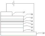
本实施例中,量子点发光二极管有多种形式,且所述量子点发光二极管可以为正置结构,也可以为倒置结构,其中正置结构的量子点发光二极管将主要以如图1所示的结构为例进行介绍。具体地,如图1所示,所述正置结构的量子点发光二极管包括从下往上依次设置的阳极10、空穴注入层11、空穴传输层12、第一量子点发光层13、间隔层14、第二量子点发光层15、电子传输层16和阴极17,所述间隔层14包括多个ZnS量子点。In this embodiment, the quantum dot light-emitting diodes have various forms, and the quantum dot light-emitting diodes may be of an upright structure or an inverted structure, wherein the quantum dot light-emitting diodes of the upright structure are mainly as shown in FIG. 1 . The structure is introduced as an example. Specifically, as shown in FIG. 1 , the quantum dot light-emitting diode of the upright structure includes an
在一种实施方式中,所述基板可以为刚性材质的基板,如玻璃等,也可以为柔性材质的基板,如PET或PI等中的一种。In one embodiment, the substrate may be a substrate of rigid material, such as glass, or a substrate of flexible material, such as one of PET or PI.
在一种实施方式中,所述阳极可以选自铟掺杂氧化锡(ITO)、氟掺杂氧化锡(FTO)、锑掺杂氧化锡(ATO)和铝掺杂氧化锌(AZO)等中的一种或多种。进一步地,所述阳极为铟掺杂氧化锡(ITO)。In one embodiment, the anode may be selected from indium-doped tin oxide (ITO), fluorine-doped tin oxide (FTO), antimony-doped tin oxide (ATO), aluminum-doped zinc oxide (AZO), and the like one or more of. Further, the anode is indium-doped tin oxide (ITO).
在一种实施方式中,所述空穴注入层的材料可以是聚(3,4-亚乙二氧基噻吩)-聚(苯乙烯磺酸)(PEDOT:PSS)及其掺有s-MoO3的衍生物(PEDOT:PSS:s-MoO3)等中的一种或多种。In one embodiment, the material of the hole injection layer may be poly(3,4-ethylenedioxythiophene)-poly(styrenesulfonic acid) (PEDOT:PSS) and its doped s-MoO One or more of derivatives of3 (PEDOT:PSS:s-MoO3 ) and the like.
在一种实施方式中,所述空穴传输层的材料为具有良好空穴传输能力的有机材料,例如可以包括但不限于聚(9,9-二辛基芴-CO-N-(4-丁基苯基)二苯胺)(TFB)、聚乙烯咔唑(PVK)、聚(N,N'双(4-丁基苯基)-N,N'-双(苯基)联苯胺)(Poly-TPD)、聚(9,9-二辛基芴-共-双-N,N-苯基-1,4-苯二胺)(PFB)、4,4’,4”-三(咔唑-9-基)三苯胺(TCTA)、4,4'-二(9-咔唑)联苯(CBP)、N,N’-二苯基-N,N’-二(3-甲基苯基)-1,1’-联苯-4,4’-二胺(TPD)、N,N’-二苯基-N,N’-(1-萘基)-1,1’-联苯-4,4’-二胺(NPB)、石墨烯和C60中的一种或多种。In one embodiment, the material of the hole transport layer is an organic material with good hole transport capability, such as but not limited to poly(9,9-dioctylfluorene-CO-N-(4- Butylphenyl)diphenylamine)(TFB), polyvinylcarbazole (PVK), poly(N,N'bis(4-butylphenyl)-N,N'-bis(phenyl)benzidine)( Poly-TPD), poly(9,9-dioctylfluorene-co-bis-N,N-phenyl-1,4-phenylenediamine) (PFB), 4,4',4"-tris(carbohydrate) oxazol-9-yl)triphenylamine (TCTA), 4,4'-bis(9-carbazole)biphenyl (CBP), N,N'-diphenyl-N,N'-bis(3-methyl) Phenyl)-1,1'-biphenyl-4,4'-diamine (TPD), N,N'-diphenyl-N,N'-(1-naphthyl)-1,1'-biphenyl One or more of benzene-4,4'-diamine (NPB), graphene and C60.
在一种实施方式中,所述空穴传输层还可以为具有空穴传输能力的无机材料,例如可以包括但不限于NiOx、MoOx、WOx、CrOx、CuO、MoSx、MoSex、WSx、WSex和CuS中的一种或多种。In one embodiment, the hole transport layer may also be an inorganic material with hole transport capability, such as but not limited toNiOx ,MoOx ,WOx ,CrOx , CuO,MoSx ,MoSex One or more of ,WSx ,WSex , and CuS.
在一种实施方式中,形成所述第一量子点发光层的量子点与形成所述第二量子点发光层的量子点相同。在一种实施方式中,所述量子点可以选自常见的红、绿、蓝三种中的一种量子点,也可以为黄光量子点。具体的,所述量子点为二元相量子点、三元相量子点或四元相量子点等,但不限于此。其中,所述二元相量子点包括但不限于CdS、CdSe、CdTe、InP、AgS、PbS、PbSe、HgS中的至少一种;所述三元相量子点包括但不限于ZnXCd1-XS、CuXIn1-XS、ZnXCd1-XSe、ZnXSe1-XS、ZnXCd1-XTe、PbSeXS1-X中的至少一种;所述四元相量子点包括但不限于ZnXCd1-XS/ZnSe、CuXIn1-XS/ZnS、ZnXCd1-XSe/ZnS、CuInSeS、ZnXCd1-XTe/ZnS、PbSeXS1-X/ZnS中的至少一种,其中0<X<1。In one embodiment, the quantum dots forming the first quantum dot light-emitting layer are the same as the quantum dots forming the second quantum dot light-emitting layer. In one embodiment, the quantum dots may be selected from one of the common red, green, and blue quantum dots, or may be yellow light quantum dots. Specifically, the quantum dots are binary-phase quantum dots, ternary-phase quantum dots, or quaternary-phase quantum dots, etc., but are not limited thereto. Wherein, the binary phase quantum dots include but are not limited to at least one of CdS, CdSe, CdTe, InP, AgS, PbS, PbSe, and HgS; the ternary phase quantum dots include but are not limited to ZnX Cd1- At least one ofX S, CuX In1-X S, ZnX Cd1-X Se, ZnX Se1-X S, ZnX Cd1-X Te, PbSeX S1-X ; the four Elemental phase quantum dots include but are not limited to ZnX Cd1-X S/ZnSe, CuX In1-X S/ZnS, ZnX Cd1-X Se/ZnS, CuInSeS, ZnX Cd1-X Te/ZnS, At least one of PbSeX S1-X /ZnS, where 0<X<1.
在一种实施方式中,所述电子传输层的材料可以选自具有良好电子传输性能的N型半导体氧化物,例如可以为但不限于N型的ZnO、TiO2、Fe2O3、SnO2、Ta2O3、AlZnO、ZnSnO、InSnO以及这些氧化物的N型掺杂等中的一种或多种。In one embodiment, the material of the electron transport layer can be selected from N-type semiconductor oxides with good electron transport properties, such as but not limited to N-type ZnO, TiO2 , Fe2 O3 , SnO2 One or more of , Ta2 O3 , AlZnO, ZnSnO, InSnO, and N-type doping of these oxides.
在一种实施方式中,所述阴极可选自铝(Al)电极、银(Ag)电极和金(Au)电极等中的一种,还可选自纳米铝线、纳米银线和纳米金线等中的一种。In one embodiment, the cathode may be selected from one of aluminum (Al) electrodes, silver (Ag) electrodes, and gold (Au) electrodes, etc., and may also be selected from nano-aluminum wires, nano-silver wires, and nano-gold electrodes. one of the lines, etc.
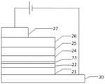
本实施例中,量子点发光二极管有多种形式,且所述量子点发光二极管可以为正置结构,也可以为倒置结构,其中倒置结构的量子点发光二极管将主要以如图2所示的结构为例进行介绍。具体地,如图2所示,所述倒置结构的量子点发光二极管包括从下往上依次设置的阴极20、电子传输层21、第二量子点发光层22、间隔层23、第一量子点发光层24、空穴传输层25、空穴注入层26和阳极27,所述间隔层包括多个ZnS量子点。In this embodiment, the quantum dot light-emitting diodes have various forms, and the quantum dot light-emitting diodes may be of an upright structure or an inverted structure, wherein the quantum dot light-emitting diodes of the inverted structure are mainly as shown in FIG. 2 . The structure is introduced as an example. Specifically, as shown in FIG. 2 , the quantum dot light emitting diode of the inverted structure includes a
在一种实施方式中,所述阴极可以选自铟掺杂氧化锡(ITO)、氟掺杂氧化锡(FTO)、锑掺杂氧化锡(ATO)和铝掺杂氧化锌(AZO)等中的一种或多种。进一步地,所述阴极为铟掺杂氧化锡(ITO)。In one embodiment, the cathode may be selected from indium-doped tin oxide (ITO), fluorine-doped tin oxide (FTO), antimony-doped tin oxide (ATO), aluminum-doped zinc oxide (AZO), and the like one or more of. Further, the cathode is indium-doped tin oxide (ITO).
在一种实施方式中,所述阳极可选自铝(Al)电极、银(Ag)电极和金(Au)电极等中的一种,还可选自纳米铝线、纳米银线和纳米金线等中的一种。In one embodiment, the anode may be selected from one of aluminum (Al) electrodes, silver (Ag) electrodes, and gold (Au) electrodes, etc., and may also be selected from nano-aluminum wires, nano-silver wires, and nano-gold electrodes. one of the lines, etc.
上述器件中,其余各层的材料选择在上文有记载,在此不再赘述。In the above device, the material selection of the remaining layers has been described above, and will not be repeated here.
请参阅图3,图3为本发明实施例提供的一种正置结构的量子点发光二极管的制备方法的流程示意图,如图3所示,包括步骤:Please refer to FIG. 3 . FIG. 3 is a schematic flowchart of a method for preparing a quantum dot light-emitting diode with an upright structure according to an embodiment of the present invention. As shown in FIG. 3 , the method includes steps:
S10、提供阳极;S10. Provide anode;
S11、在所述阳极上形成第一量子点发光层;S11, forming a first quantum dot light-emitting layer on the anode;
S12、在所述第一量子点发光层上形成间隔层,所述间隔层包括多个ZnS量子点;S12, forming a spacer layer on the first quantum dot light-emitting layer, the spacer layer comprising a plurality of ZnS quantum dots;
S13、在所述间隔层上形成第二量子点发光层;S13, forming a second quantum dot light-emitting layer on the spacer layer;
S14、在所述第二量子点发光层上形成阴极,得到量子点发光二极管。S14, forming a cathode on the second quantum dot light-emitting layer to obtain a quantum dot light-emitting diode.
请参阅图4,图4为本发明实施例提供的一种倒置结构的量子点发光二极管的制备方法的流程示意图,如图4所示,包括步骤:Please refer to FIG. 4 . FIG. 4 is a schematic flowchart of a method for manufacturing a quantum dot light-emitting diode with an inverted structure according to an embodiment of the present invention. As shown in FIG. 4 , the method includes steps:
S20、提供阴极;S20, provide cathode;
S21、在所述阴极上形成第二量子点发光层;S21, forming a second quantum dot light-emitting layer on the cathode;
S22、在所述第二量子点发光层上形成间隔层,所述间隔层包括多个ZnS量子点;S22, forming a spacer layer on the second quantum dot light-emitting layer, the spacer layer comprising a plurality of ZnS quantum dots;
S23、在所述间隔层上形成第一量子点发光层;S23, forming a first quantum dot light-emitting layer on the spacer layer;
S24、在所述第一量子点发光层上形成阳极,得到量子点发光二极管。S24, forming an anode on the first quantum dot light-emitting layer to obtain a quantum dot light-emitting diode.
本实施例中,采用将原本一层厚的量子点发光层设置为相对较薄的两层量子点发光层(第一量子点发光层和第二量子点发光层),在两层量子点发光层之间加入一层间隔层(所述间隔层包括多个ZnS量子点)的方式,利用ZnS的高带隙(3.65eV左右),穿插进两层相对较薄的量子点发光层之间作为阻挡,避免了原本设置一层厚的量子点发光层会带来的荧光共振能量转移(FRET)问题,确保了最终的器件亮度、量子效率以及寿命。本实施例中,所述间隔层,使得两层量子点之间具有一定的距离,最终令辐射性的激子复合发生在量子点发光层内,从而使得器件亮度以及量子效率得到提升。同时,所述间隔层还可以作为电荷注入层,将一定的电荷转移进QD,使得效率进一步得到提升。In this embodiment, two quantum dot light-emitting layers (a first quantum dot light-emitting layer and a second quantum dot light-emitting layer) are used to set the original one-layer thick quantum dot light-emitting layer to a relatively thin quantum dot light-emitting layer, and the two quantum dot light-emitting layers emit light. A spacer layer (the spacer layer includes a plurality of ZnS quantum dots) is added between the layers, using the high band gap of ZnS (about 3.65eV), interspersed between two relatively thin quantum dot light-emitting layers As a barrier, it avoids the fluorescence resonance energy transfer (FRET) problem caused by setting a thick quantum dot light-emitting layer originally, and ensures the final device brightness, quantum efficiency and lifetime. In this embodiment, the spacer layer has a certain distance between the two layers of quantum dots, so that radiative exciton recombination occurs in the quantum dot light-emitting layer finally, so that the brightness and quantum efficiency of the device are improved. At the same time, the spacer layer can also be used as a charge injection layer to transfer certain charges into the QD, so that the efficiency is further improved.
在一种实施方式中,所述间隔层由ZnS量子点组成。In one embodiment, the spacer layer consists of ZnS quantum dots.
在一种实施方式中,所述第一量子点发光层与第二量子点发光层均由量子点组成,所述第一量子点发光层的量子点的平均粒径与所述ZnS量子点的平均粒径的比值小于或等于1.5并且大于或等于0.5,且所述第二量子点发光层的量子点的平均粒径与所述ZnS量子点的平均粒径的比值小于或等于1.5并且大于或等于0.5。例如,第一量子点发光层的量子点的平均粒径为15nm,ZnS量子点的平均粒径为10nm,比值为1.5;或者第一量子点发光层的量子点的平均粒径为15nm,ZnS量子点的平均粒径为15nm,比值为1;所述第一量子点发光层的量子点的平均粒径与所述ZnS量子点的平均粒径的比值可以取值为0.8、0.9、1、1.1、1.2、1.3、1.4或1.5等。例如,第二量子点发光层的量子点的平均粒径为15nm,ZnS量子点的平均粒径为10nm,比值为1.5;或者第二量子点发光层的量子点的平均粒径为15nm,ZnS量子点的平均粒径为15nm,比值为1;所述第二量子点发光层的量子点的平均粒径与所述ZnS量子点的平均粒径的比值可以取值为0.8、0.9、1、1.1、1.2、1.3、1.4或1.5等。In one embodiment, the first quantum dot light-emitting layer and the second quantum dot light-emitting layer are both composed of quantum dots, and the average particle size of the quantum dots in the first quantum dot light-emitting layer is the same as that of the ZnS quantum dots. The ratio of the average particle diameter is less than or equal to 1.5 and greater than or equal to 0.5, and the ratio of the average particle diameter of the quantum dots of the second quantum dot light-emitting layer to the average particle diameter of the ZnS quantum dots is less than or equal to 1.5 and greater than or is equal to 0.5. For example, the average particle size of the quantum dots in the first quantum dot light-emitting layer is 15 nm, the average particle size of the ZnS quantum dots is 10 nm, and the ratio is 1.5; or the average particle size of the quantum dots in the first quantum dot light-emitting layer is 15 nm, the ZnS The average particle size of the quantum dots is 15nm, and the ratio is 1; the ratio of the average particle size of the quantum dots of the first quantum dot light-emitting layer to the average particle size of the ZnS quantum dots can be 0.8, 0.9, 1, 1.1, 1.2, 1.3, 1.4 or 1.5 etc. For example, the average particle size of the quantum dots in the second quantum dot light-emitting layer is 15 nm, and the average particle size of the ZnS quantum dots is 10 nm, and the ratio is 1.5; or the average particle size of the quantum dots in the second quantum dot light-emitting layer is 15 nm, and the ZnS The average particle size of the quantum dots is 15nm, and the ratio is 1; the ratio of the average particle size of the quantum dots of the second quantum dot light-emitting layer to the average particle size of the ZnS quantum dots can be 0.8, 0.9, 1, 1.1, 1.2, 1.3, 1.4 or 1.5 etc.
需说明的是,量子点实际的粒径分布在一个区间。本实施方式中的量子点的平均粒径可以通过结合本领域的常见的测试粒径的方法统计得到,例如可通过结合透射电子电镜(TEM)的表征方法统计得到(可以结合digitalmicrograph软件或者imageJ软件直接统计电镜图片),或者通过结合X射线衍射法(XRD)求得(如可以结合常用的Scherrel公式—谢乐公式),或者粒度分析仪或Zeta电势仪的表征方法得到,或者结合纳米材料领域其他常见的表征粒径的方法得到。由于本实施方式中的量子点的平均粒径可以通过结合本领域的常见的测试粒径的方法统计得到,在此不再详述,具体可以参考现有技术。It should be noted that the actual particle size distribution of the quantum dots is in an interval. The average particle size of the quantum dots in this embodiment can be statistically obtained by combining the common particle diameter testing methods in the art, for example, by combining with the characterization method of transmission electron microscopy (TEM) (which can be combined with digitalmicrograph software or imageJ software. Direct statistical electron microscope pictures), or obtained by combining X-ray diffraction (XRD) (for example, it can be combined with the commonly used Scherrel formula - Scherrer formula), or obtained by particle size analyzer or Zeta potentiometer characterization method, or combined with the field of nanomaterials Other common methods of characterizing particle size are obtained. Since the average particle size of the quantum dots in this embodiment can be obtained statistically by combining with the common method of testing particle size in the art, it will not be described in detail here, and specific reference may be made to the prior art.
在一种实施方式中,所述间隔层的厚度小于或等于所述第一量子点发光层的厚度,和/或所述间隔层的厚度小于或等于所述第二量子点发光层的厚度。如此,间隔层厚度适中。因为其电致发光的能力远弱于量子点发光层本身,故过厚的情况下可能会使得同电压下的亮度及效率变低。In one embodiment, the thickness of the spacer layer is less than or equal to the thickness of the first quantum dot light-emitting layer, and/or the thickness of the spacer layer is less than or equal to the thickness of the second quantum dot light-emitting layer. Thus, the thickness of the spacer layer is moderate. Because its electroluminescence capability is much weaker than that of the quantum dot light-emitting layer itself, if it is too thick, the brightness and efficiency at the same voltage may be reduced.
在一些例子中,所述间隔层的厚度小于或等于所述第一量子点发光层的厚度,且所述间隔层的厚度小于或等于所述第二量子点发光层的厚度。在另一些例子中,所述间隔层的厚度小于或等于所述第一量子点发光层的厚度。在又一些例子中,所述间隔层的厚度小于或等于所述第二量子点发光层的厚度。In some examples, the thickness of the spacer layer is less than or equal to the thickness of the first quantum dot light-emitting layer, and the thickness of the spacer layer is less than or equal to the thickness of the second quantum dot light-emitting layer. In other examples, the thickness of the spacer layer is less than or equal to the thickness of the first quantum dot light-emitting layer. In still other examples, the thickness of the spacer layer is less than or equal to the thickness of the second quantum dot light-emitting layer.
在一种实施方式中,所述间隔层的厚度为10~16nm。当间隔层的厚度逐渐增加,使得两层量子点之间的距离足够大,辐射性的激子复合发生在量子点发光层内,从而使得器件亮度得到提升。当然间隔层本身也不能过厚,因为其电致发光的能力远弱于量子点发光层本身,故过厚的情况下会使得同电压下的亮度及效率变低。In one embodiment, the thickness of the spacer layer is 10-16 nm. When the thickness of the spacer layer is gradually increased, the distance between the two layers of quantum dots is large enough, and the radiative exciton recombination occurs in the light-emitting layer of the quantum dots, thereby improving the brightness of the device. Of course, the spacer layer itself cannot be too thick, because its electroluminescence capability is far weaker than that of the quantum dot light-emitting layer itself, so too thick will reduce the brightness and efficiency under the same voltage.
在一种实施方式中,所述第一量子点发光层的厚度为15~25nm,所述第二量子点发光层的厚度为15~25nm。需说明的是,所述第一量子点发光层的厚度与所述第二量子点发光层的厚度可以相同,也可以不同。In one embodiment, the thickness of the first quantum dot light-emitting layer is 15-25 nm, and the thickness of the second quantum-dot light-emitting layer is 15-25 nm. It should be noted that the thickness of the first quantum dot light-emitting layer and the thickness of the second quantum dot light-emitting layer may be the same or different.
在一种实施方式中,形成所述第一量子点发光层的材料与形成所述第二量子点发光层的材料相同。因为本实施例主要目的是增强量子点发光二极管的亮度,量子点发光二极管本身的优势也在于材料的半峰宽较窄,如果第一量子点发光层与第二量子点发光层使用不同种量子点材料,有可能会改变其发光峰位或使得半峰宽增大,保持材料一致可以确保其原发光色彩纯度的同时进行发光亮度的改进。In one embodiment, the material for forming the first quantum dot light-emitting layer is the same as the material for forming the second quantum dot light-emitting layer. Because the main purpose of this embodiment is to enhance the brightness of the quantum dot light-emitting diode, the advantage of the quantum dot light-emitting diode itself is that the half-peak width of the material is narrow. If the first quantum dot light-emitting layer and the second quantum dot light-emitting layer use different quantum dots Dot materials may change their luminescence peak positions or increase the half-peak width. Keeping the materials consistent can ensure the purity of the original luminescence color and improve the luminescence brightness at the same time.
本实施例中,量子点发光二极管有多种形式,下面以图1所示结构为例,对正置结构的量子点发光二极管的制备方法进行介绍。图1所示的正置结构的量子点发光二极管的制备方法,包括以下步骤:In this embodiment, the quantum dot light emitting diode has various forms. The following takes the structure shown in FIG. 1 as an example to introduce the preparation method of the quantum dot light emitting diode with the upright structure. The preparation method of the quantum dot light-emitting diode with the upright structure shown in FIG. 1 includes the following steps:
S101、在阳极10上形成空穴注入层11;S101, forming a
S102、在空穴注入层11上形成空穴传输层12;S102, forming a
S103、在空穴传输层12上形成第一量子点发光层13;S103, forming a first quantum dot light-emitting
S104、在第一量子点发光层13上形成间隔层14,所述间隔层14包括多个ZnS量子点;S104, forming a
S105、在间隔层14上形成第二层量子点发光层15;S105, forming a second quantum dot light-emitting
S106、在第二层量子点发光层15上形成电子传输层16;S106, forming an
S107、制作阴极17,得到正置结构量子点发光二极管。S107 , the
本实施例中,量子点发光二极管有多种形式,下面以图2所示结构为例,对倒置结构的量子点发光二极管的制备方法进行介绍。图2所示的倒置结构的量子点发光二极管的制备方法,包括以下步骤:In this embodiment, the quantum dot light emitting diode has various forms. The following takes the structure shown in FIG. 2 as an example to introduce the manufacturing method of the quantum dot light emitting diode with the inverted structure. The preparation method of the quantum dot light-emitting diode with the inverted structure shown in FIG. 2 includes the following steps:
S201、在阴极20上形成电子传输层21;S201, forming an
S202、在电子传输层21上形成第二量子点发光层22;S202, forming a second quantum dot light-emitting
S203、在第二量子点发光层22上形成间隔层23,所述间隔层23包括多个ZnS量子点;S203, forming a
S204、在间隔层23上形成第一层量子点发光层24;S204, forming a first quantum dot light-emitting
S205、在第一层量子点发光层24上形成空穴传输层25;S205, forming a
S205、在空穴传输层25上形成空穴注入层26;S205, forming a
S206、制作阳极27,得到倒置结构量子点发光二极管。S206, the
在一种实施方式中,对得到的量子点发光二极管进行封装处理。其中所述封装处理可采用常用的机器封装,也可以采用手动封装。优选的,所述封装处理的环境中,氧含量和水含量均低于0.1ppm,以保证器件的稳定性。In one embodiment, the obtained quantum dot light-emitting diode is packaged. The encapsulation process can be packaged by a commonly used machine, or can also be packaged manually. Preferably, in the packaging process environment, the oxygen content and the water content are both lower than 0.1 ppm to ensure the stability of the device.
本实施例中,各层制备方法可以是化学法或物理法,其中化学法包括但不限于化学气相沉积法、连续离子层吸附与反应法、阳极氧化法、电解沉积法、共沉淀法中的一种或多种;物理法包括但不限于溶液法(如旋涂法、印刷法、刮涂法、浸渍提拉法、浸泡法、喷涂法、滚涂法、浇铸法、狭缝式涂布法或条状涂布法等)、蒸镀法(如热蒸镀法、电子束蒸镀法、磁控溅射法或多弧离子镀膜法等)、沉积法(如物理气相沉积法、原子层沉积法、脉冲激光沉积法等)中的一种或多种。In this embodiment, the preparation method of each layer may be a chemical method or a physical method, wherein the chemical method includes but is not limited to chemical vapor deposition method, continuous ion layer adsorption and reaction method, anodic oxidation method, electrolytic deposition method, and co-precipitation method. One or more; physical methods include but are not limited to solution methods (such as spin coating, printing, blade coating, dip-pulling, immersion, spraying, roll coating, casting, slot coating method or strip coating method, etc.), evaporation method (such as thermal evaporation method, electron beam evaporation method, magnetron sputtering method or multi-arc ion coating method, etc.), deposition method (such as physical vapor deposition method, atomic One or more of layer deposition method, pulsed laser deposition method, etc.).
下面通过具体的实施例对本发明作进一步地说明。The present invention will be further described below through specific embodiments.
实施例1Example 1
正置结构QLED器件的制备:Fabrication of upright structure QLED devices:
S11、在ITO衬底上旋涂一层PEDOT:PSS:s-MoO3空穴注入层,并在空气中150℃下进行退火;S11, spin-coating a PEDOT:PSS:s- MoO3 hole injection layer on the ITO substrate, and annealing at 150°C in air;
S12、于氮气气氛中,在空穴注入层上旋涂一层20nm PVK空穴传输层,并在150℃下进行退火;S12. In a nitrogen atmosphere, spin-coat a 20nm PVK hole transport layer on the hole injection layer, and anneal at 150°C;
S13、在空穴传输层上旋涂一层20nm CdSe/ZnS第一量子点发光层,并放置在空气中1min后拿回氮气手套箱中;S13, spin-coat a layer of 20nm CdSe/ZnS first quantum dot light-emitting layer on the hole transport layer, and place it in the air for 1 min, then take it back to the nitrogen glove box;
S14、在第一量子点发光层上旋涂一层15nm的ZnS间隔层,并放置在空气中1min后拿回氮气手套箱中;S14, spin-coat a layer of 15nm ZnS spacer layer on the first quantum dot light-emitting layer, and place it in the air for 1 min and then take it back to the nitrogen glove box;
S15、在ZnS间隔层上旋涂一层20nm CdSe/ZnS第二量子点发光层,并在80℃下进行退火;S15, spin-coating a 20nm CdSe/ZnS second quantum dot light-emitting layer on the ZnS spacer layer, and annealing at 80°C;
S16、在第二量子点发光层上以磁控溅射的方法镀上一层30nm AZO电子传输层;S16, plating a layer of 30nm AZO electron transport layer on the second quantum dot light-emitting layer by magnetron sputtering;
S17、在电子传输层上蒸镀80nm Al电极;S17, 80nm Al electrode is evaporated on the electron transport layer;
S18、经封装后得到正置结构QLED器件。S18 , the upright structure QLED device is obtained after encapsulation.
实施例2Example 2
倒置结构QLED器件的制备:Fabrication of inverted-structure QLED devices:
S21、于氮气气氛中,在ITO衬底上沉积一层50nm ZnO电子传输层;S21, in a nitrogen atmosphere, deposit a layer of 50nm ZnO electron transport layer on the ITO substrate;
S22、在电子传输层上旋涂一层15nm的CdZnSeS/ZnS第二量子点发光层,并放置在空气中1min后拿回氮气手套箱中;S22, spin coating a layer of 15nm CdZnSeS/ZnS second quantum dot light-emitting layer on the electron transport layer, and place it in the air for 1 min and then take it back to the nitrogen glove box;
S23、在第二量子点发光层上旋涂一层10nm的ZnS间隔层,并放置在空气中1min后拿回氮气手套箱中;S23, spin-coat a layer of 10nm ZnS spacer layer on the second quantum dot light-emitting layer, and place it in the air for 1min and then take it back to the nitrogen glove box;
S24、在ZnS间隔层上旋涂一层15nm的CdZnSeS/ZnS第一量子点发光层,并在100℃下进行退火;S24, spin-coating a 15nm CdZnSeS/ZnS first quantum dot light-emitting layer on the ZnS spacer layer, and annealing at 100°C;
S25、在第一量子点发光层上旋涂一层25nm NPB空穴传输层,并在80℃下进行退火;S25, spin-coating a 25nm NPB hole transport layer on the first quantum dot light-emitting layer, and annealing at 80°C;
S26、在空穴传输层上喷镀一层PEDOT:PSS空穴注入层;S26, sputtering a layer of PEDOT:PSS hole injection layer on the hole transport layer;
S27、在空穴注入层上蒸镀90nm Ag电极;S27, 90nm Ag electrode is evaporated on the hole injection layer;
S28、经封装后得到倒置结构QLED器件。S28, an inverted structure QLED device is obtained after packaging.
综上所述,本发明提供的一种量子点发光二极管及其制备方法,本发明中,采用将原本一层厚的量子点发光层设置为相对较薄的两层量子点发光层(第一量子点发光层和第二量子点发光层),在两层量子点发光层之间加入一层ZnS间隔层的方式,利用ZnS的高带隙(3.65eV左右),穿插进两层相对较薄的量子点发光层之间作为阻挡,避免了原本设置一层厚的量子点发光层会带来的荧光共振能量转移(FRET)问题,确保了最终的器件亮度、量子效率以及寿命。本发明中,所述ZnS间隔层,使得两层量子点之间具有一定的距离,最终令辐射性的激子复合发生在量子点发光层内,从而使得器件亮度以及量子效率得到提升。同时,所述ZnS间隔层还可以作为电荷注入层,将一定的电荷转移进QD,使得效率进一步得到提升。To sum up, the present invention provides a quantum dot light-emitting diode and a preparation method thereof. In the present invention, the quantum dot light-emitting layer with one thick layer is set to a relatively thin two-layer quantum dot light-emitting layer (the first The quantum dot light-emitting layer and the second quantum dot light-emitting layer), a ZnS spacer layer is added between the two quantum dot light-emitting layers, and the high band gap (about 3.65eV) of ZnS is used to intersperse the two layers. The thin quantum dot light-emitting layer acts as a barrier, avoiding the fluorescence resonance energy transfer (FRET) problem caused by setting a thick quantum dot light-emitting layer, and ensuring the final device brightness, quantum efficiency and lifetime. In the present invention, the ZnS spacer layer makes a certain distance between the two layers of quantum dots, and finally makes the radiative exciton recombination occur in the quantum dot light-emitting layer, thereby improving the brightness and quantum efficiency of the device. At the same time, the ZnS spacer layer can also be used as a charge injection layer to transfer certain charges into the QD, so that the efficiency is further improved.
应当理解的是,本发明的应用不限于上述的举例,对本领域普通技术人员来说,可以根据上述说明加以改进或变换,所有这些改进和变换都应属于本发明所附权利要求的保护范围。It should be understood that the application of the present invention is not limited to the above examples. For those of ordinary skill in the art, improvements or transformations can be made according to the above descriptions, and all these improvements and transformations should belong to the protection scope of the appended claims of the present invention.
Claims (10)
Translated fromChinesePriority Applications (2)
| Application Number | Priority Date | Filing Date | Title |
|---|---|---|---|
| CN201911425210.4ACN113130794B (en) | 2019-12-31 | 2019-12-31 | Quantum dot light-emitting diode and preparation method thereof |
| PCT/CN2020/139788WO2021136119A1 (en) | 2019-12-31 | 2020-12-27 | Quantum dot light emitting diode and preparation method therefor |
Applications Claiming Priority (1)
| Application Number | Priority Date | Filing Date | Title |
|---|---|---|---|
| CN201911425210.4ACN113130794B (en) | 2019-12-31 | 2019-12-31 | Quantum dot light-emitting diode and preparation method thereof |
Publications (2)
| Publication Number | Publication Date |
|---|---|
| CN113130794Atrue CN113130794A (en) | 2021-07-16 |
| CN113130794B CN113130794B (en) | 2022-12-13 |
Family
ID=76687363
Family Applications (1)
| Application Number | Title | Priority Date | Filing Date |
|---|---|---|---|
| CN201911425210.4AActiveCN113130794B (en) | 2019-12-31 | 2019-12-31 | Quantum dot light-emitting diode and preparation method thereof |
Country Status (2)
| Country | Link |
|---|---|
| CN (1) | CN113130794B (en) |
| WO (1) | WO2021136119A1 (en) |
Cited By (1)
| Publication number | Priority date | Publication date | Assignee | Title |
|---|---|---|---|---|
| CN112736207A (en)* | 2020-12-30 | 2021-04-30 | 广东聚华印刷显示技术有限公司 | QLED device, preparation method of QLED device and display device |
Citations (20)
| Publication number | Priority date | Publication date | Assignee | Title |
|---|---|---|---|---|
| US20070069202A1 (en)* | 2005-09-27 | 2007-03-29 | Choi Byoung L | Light-emitting device comprising semiconductor nanocrystal layer free of voids and method for producing the same |
| JP2009087754A (en)* | 2007-09-28 | 2009-04-23 | Dainippon Printing Co Ltd | Light emitting element |
| WO2009081918A1 (en)* | 2007-12-26 | 2009-07-02 | Idemitsu Kosan Co., Ltd. | Organic/inorganic hybrid electroluminescent element |
| US20130146838A1 (en)* | 2011-12-09 | 2013-06-13 | Samsung Electronics Co., Ltd. | Quantum dot device including different kinds of quantum dot layers |
| CN105098084A (en)* | 2015-06-16 | 2015-11-25 | 武汉华星光电技术有限公司 | Quantum dot-based light-emitting diode and display device |
| CN105609535A (en)* | 2016-01-15 | 2016-05-25 | 京东方科技集团股份有限公司 | Display substrate, display device and manufacturing method of display device |
| CN106206967A (en)* | 2016-08-10 | 2016-12-07 | 京东方科技集团股份有限公司 | Quantum dot light emitting device and preparation method thereof, display device |
| CN107093673A (en)* | 2017-05-17 | 2017-08-25 | 南昌航空大学 | Multi-layer quantum white point luminescent device |
| US20180019371A1 (en)* | 2016-03-17 | 2018-01-18 | Apple Inc. | Quantum dot spacing for high efficiency quantum dot led displays |
| WO2018062677A1 (en)* | 2016-09-28 | 2018-04-05 | 경북대학교 산학협력단 | White light quantum dots based light emitting diode and manufacturing method therefor |
| KR20180047820A (en)* | 2016-11-01 | 2018-05-10 | 엘지디스플레이 주식회사 | Quantum dot emitting diode and Quantum dot display device including the same |
| US20190097150A1 (en)* | 2017-09-22 | 2019-03-28 | Shenzhen China Star Optoelectronics Semiconductor Display Technology Co., Ltd. | Quantum dot light-emitting diode and display device |
| CN109935725A (en)* | 2017-12-15 | 2019-06-25 | Tcl集团股份有限公司 | Light emitting diode with quantum dots and its preparation method and application |
| CN109980105A (en)* | 2017-12-28 | 2019-07-05 | Tcl集团股份有限公司 | A kind of QLED device |
| CN110176548A (en)* | 2019-05-21 | 2019-08-27 | 东南大学 | A kind of dual emission formula white light quanta point light emitting diode and preparation method thereof |
| WO2019166972A1 (en)* | 2018-03-01 | 2019-09-06 | Sabic Global Technologies B.V. | Perovskite quantum dot layer |
| CN110212105A (en)* | 2019-06-26 | 2019-09-06 | 苏州星烁纳米科技有限公司 | Quantum dot light emitting device and preparation method thereof, lighting device |
| CN110416421A (en)* | 2018-04-28 | 2019-11-05 | Tcl集团股份有限公司 | A kind of quantum dot film and light emitting diode with quantum dots |
| CN110521012A (en)* | 2016-12-01 | 2019-11-29 | 纳米系统公司 | Quantum dot LED with spacer particles |
| CN110611033A (en)* | 2019-08-29 | 2019-12-24 | 深圳市华星光电半导体显示技术有限公司 | White light quantum dot light emitting diode device and preparation method thereof |
Family Cites Families (4)
| Publication number | Priority date | Publication date | Assignee | Title |
|---|---|---|---|---|
| CN109980096B (en)* | 2017-12-27 | 2020-09-11 | Tcl科技集团股份有限公司 | QLED device and preparation method thereof |
| CN110890470A (en)* | 2018-09-07 | 2020-03-17 | Tcl集团股份有限公司 | Quantum dot light-emitting diode |
| CN111129333B (en)* | 2019-12-30 | 2022-08-19 | 广东聚华印刷显示技术有限公司 | QLED device, display device and preparation method of QLED device |
| CN111416053B (en)* | 2020-05-11 | 2023-05-30 | 京东方科技集团股份有限公司 | A quantum dot light-emitting device and its preparation method, display panel, and display device |
- 2019
- 2019-12-31CNCN201911425210.4Apatent/CN113130794B/enactiveActive
- 2020
- 2020-12-27WOPCT/CN2020/139788patent/WO2021136119A1/ennot_activeCeased
Patent Citations (20)
| Publication number | Priority date | Publication date | Assignee | Title |
|---|---|---|---|---|
| US20070069202A1 (en)* | 2005-09-27 | 2007-03-29 | Choi Byoung L | Light-emitting device comprising semiconductor nanocrystal layer free of voids and method for producing the same |
| JP2009087754A (en)* | 2007-09-28 | 2009-04-23 | Dainippon Printing Co Ltd | Light emitting element |
| WO2009081918A1 (en)* | 2007-12-26 | 2009-07-02 | Idemitsu Kosan Co., Ltd. | Organic/inorganic hybrid electroluminescent element |
| US20130146838A1 (en)* | 2011-12-09 | 2013-06-13 | Samsung Electronics Co., Ltd. | Quantum dot device including different kinds of quantum dot layers |
| CN105098084A (en)* | 2015-06-16 | 2015-11-25 | 武汉华星光电技术有限公司 | Quantum dot-based light-emitting diode and display device |
| CN105609535A (en)* | 2016-01-15 | 2016-05-25 | 京东方科技集团股份有限公司 | Display substrate, display device and manufacturing method of display device |
| US20180019371A1 (en)* | 2016-03-17 | 2018-01-18 | Apple Inc. | Quantum dot spacing for high efficiency quantum dot led displays |
| CN106206967A (en)* | 2016-08-10 | 2016-12-07 | 京东方科技集团股份有限公司 | Quantum dot light emitting device and preparation method thereof, display device |
| WO2018062677A1 (en)* | 2016-09-28 | 2018-04-05 | 경북대학교 산학협력단 | White light quantum dots based light emitting diode and manufacturing method therefor |
| KR20180047820A (en)* | 2016-11-01 | 2018-05-10 | 엘지디스플레이 주식회사 | Quantum dot emitting diode and Quantum dot display device including the same |
| CN110521012A (en)* | 2016-12-01 | 2019-11-29 | 纳米系统公司 | Quantum dot LED with spacer particles |
| CN107093673A (en)* | 2017-05-17 | 2017-08-25 | 南昌航空大学 | Multi-layer quantum white point luminescent device |
| US20190097150A1 (en)* | 2017-09-22 | 2019-03-28 | Shenzhen China Star Optoelectronics Semiconductor Display Technology Co., Ltd. | Quantum dot light-emitting diode and display device |
| CN109935725A (en)* | 2017-12-15 | 2019-06-25 | Tcl集团股份有限公司 | Light emitting diode with quantum dots and its preparation method and application |
| CN109980105A (en)* | 2017-12-28 | 2019-07-05 | Tcl集团股份有限公司 | A kind of QLED device |
| WO2019166972A1 (en)* | 2018-03-01 | 2019-09-06 | Sabic Global Technologies B.V. | Perovskite quantum dot layer |
| CN110416421A (en)* | 2018-04-28 | 2019-11-05 | Tcl集团股份有限公司 | A kind of quantum dot film and light emitting diode with quantum dots |
| CN110176548A (en)* | 2019-05-21 | 2019-08-27 | 东南大学 | A kind of dual emission formula white light quanta point light emitting diode and preparation method thereof |
| CN110212105A (en)* | 2019-06-26 | 2019-09-06 | 苏州星烁纳米科技有限公司 | Quantum dot light emitting device and preparation method thereof, lighting device |
| CN110611033A (en)* | 2019-08-29 | 2019-12-24 | 深圳市华星光电半导体显示技术有限公司 | White light quantum dot light emitting diode device and preparation method thereof |
Cited By (1)
| Publication number | Priority date | Publication date | Assignee | Title |
|---|---|---|---|---|
| CN112736207A (en)* | 2020-12-30 | 2021-04-30 | 广东聚华印刷显示技术有限公司 | QLED device, preparation method of QLED device and display device |
Also Published As
| Publication number | Publication date |
|---|---|
| CN113130794B (en) | 2022-12-13 |
| WO2021136119A1 (en) | 2021-07-08 |
Similar Documents
| Publication | Publication Date | Title |
|---|---|---|
| US11870004B2 (en) | Metal oxide nanoparticles surface-treated with metal ion, quantum dot-light-emitting device comprising the same and method for fabricating the same | |
| CN111384278B (en) | A kind of quantum dot light-emitting diode and preparation method thereof | |
| CN105552244B (en) | A kind of luminescent device and preparation method thereof, display device | |
| US20170186909A1 (en) | Quantum dot and light emitting diode including the same | |
| KR101620870B1 (en) | Light-emitting diode comprising surface modified zinc oxide as material for electron transport layer | |
| CN108807720B (en) | Functionalized cathode, QLED, preparation method, light-emitting module and display device | |
| CN105609651A (en) | High-efficiency quantum dot light-emitting diodes with self-assembled polymer hole-transport layer structure | |
| CN106384767A (en) | Quantum dot LED, manufacturing method thereof, light emitting module group and display apparatus | |
| JP7640573B2 (en) | Nanomaterial, its manufacturing method, and quantum dot light-emitting diode | |
| KR20130008892A (en) | Quantum-dot light emitting diode and method for fabricating the same | |
| US12200953B2 (en) | Light-emitting device | |
| CN110649170B (en) | Quantum dot light-emitting diode and manufacturing method thereof | |
| CN111384255A (en) | Quantum dot light-emitting diode and preparation method thereof | |
| WO2019024513A1 (en) | Quantum dot light emitting diode and preparation method therefor | |
| CN113243054B (en) | Display device and method for manufacturing the same | |
| CN111384254B (en) | Quantum dot light-emitting diode | |
| CN113130794B (en) | Quantum dot light-emitting diode and preparation method thereof | |
| CN113130631B (en) | A kind of heterojunction nanomaterial and its preparation method, thin film, quantum dot light-emitting diode | |
| CN115477944A (en) | Quantum dot material, quantum dot light-emitting diode and preparation method thereof | |
| CN114695714B (en) | Quantum dot light emitting diode and preparation method thereof | |
| CN116033785A (en) | light emitting device | |
| CN116437692A (en) | Photoelectric device and preparation method thereof | |
| WO2022233145A1 (en) | Quantum dot electroluminescent device | |
| CN114695721A (en) | A kind of quantum dot light-emitting diode and preparation method thereof | |
| WO2023051461A1 (en) | Molybdenum oxide nanomaterial, preparation method therefor, and photoelectric device |
Legal Events
| Date | Code | Title | Description |
|---|---|---|---|
| PB01 | Publication | ||
| PB01 | Publication | ||
| SE01 | Entry into force of request for substantive examination | ||
| SE01 | Entry into force of request for substantive examination | ||
| CB02 | Change of applicant information | ||
| CB02 | Change of applicant information | Address after:516006 TCL science and technology building, No. 17, Huifeng Third Road, Zhongkai high tech Zone, Huizhou City, Guangdong Province Applicant after:TCL Technology Group Co.,Ltd. Address before:516006 Guangdong province Huizhou Zhongkai hi tech Development Zone No. nineteen District Applicant before:TCL Corp. | |
| GR01 | Patent grant | ||
| GR01 | Patent grant |