CN113130463B - A light-emitting substrate, its preparation method, and a display device - Google Patents
A light-emitting substrate, its preparation method, and a display deviceDownload PDFInfo
- Publication number
- CN113130463B CN113130463BCN202110409330.6ACN202110409330ACN113130463BCN 113130463 BCN113130463 BCN 113130463BCN 202110409330 ACN202110409330 ACN 202110409330ACN 113130463 BCN113130463 BCN 113130463B
- Authority
- CN
- China
- Prior art keywords
- lines
- power supply
- fixed voltage
- pixel
- line
- Prior art date
- Legal status (The legal status is an assumption and is not a legal conclusion. Google has not performed a legal analysis and makes no representation as to the accuracy of the status listed.)
- Active
Links
Images


Classifications
- H—ELECTRICITY
- H01—ELECTRIC ELEMENTS
- H01L—SEMICONDUCTOR DEVICES NOT COVERED BY CLASS H10
- H01L25/00—Assemblies consisting of a plurality of semiconductor or other solid state devices
- H01L25/03—Assemblies consisting of a plurality of semiconductor or other solid state devices all the devices being of a type provided for in a single subclass of subclasses H10B, H10D, H10F, H10H, H10K or H10N, e.g. assemblies of rectifier diodes
- H01L25/04—Assemblies consisting of a plurality of semiconductor or other solid state devices all the devices being of a type provided for in a single subclass of subclasses H10B, H10D, H10F, H10H, H10K or H10N, e.g. assemblies of rectifier diodes the devices not having separate containers
- H01L25/075—Assemblies consisting of a plurality of semiconductor or other solid state devices all the devices being of a type provided for in a single subclass of subclasses H10B, H10D, H10F, H10H, H10K or H10N, e.g. assemblies of rectifier diodes the devices not having separate containers the devices being of a type provided for in group H10H20/00
- H01L25/0753—Assemblies consisting of a plurality of semiconductor or other solid state devices all the devices being of a type provided for in a single subclass of subclasses H10B, H10D, H10F, H10H, H10K or H10N, e.g. assemblies of rectifier diodes the devices not having separate containers the devices being of a type provided for in group H10H20/00 the devices being arranged next to each other
- G—PHYSICS
- G09—EDUCATION; CRYPTOGRAPHY; DISPLAY; ADVERTISING; SEALS
- G09G—ARRANGEMENTS OR CIRCUITS FOR CONTROL OF INDICATING DEVICES USING STATIC MEANS TO PRESENT VARIABLE INFORMATION
- G09G3/00—Control arrangements or circuits, of interest only in connection with visual indicators other than cathode-ray tubes
- G09G3/20—Control arrangements or circuits, of interest only in connection with visual indicators other than cathode-ray tubes for presentation of an assembly of a number of characters, e.g. a page, by composing the assembly by combination of individual elements arranged in a matrix no fixed position being assigned to or needed to be assigned to the individual characters or partial characters
- G09G3/22—Control arrangements or circuits, of interest only in connection with visual indicators other than cathode-ray tubes for presentation of an assembly of a number of characters, e.g. a page, by composing the assembly by combination of individual elements arranged in a matrix no fixed position being assigned to or needed to be assigned to the individual characters or partial characters using controlled light sources
- G09G3/30—Control arrangements or circuits, of interest only in connection with visual indicators other than cathode-ray tubes for presentation of an assembly of a number of characters, e.g. a page, by composing the assembly by combination of individual elements arranged in a matrix no fixed position being assigned to or needed to be assigned to the individual characters or partial characters using controlled light sources using electroluminescent panels
- G09G3/32—Control arrangements or circuits, of interest only in connection with visual indicators other than cathode-ray tubes for presentation of an assembly of a number of characters, e.g. a page, by composing the assembly by combination of individual elements arranged in a matrix no fixed position being assigned to or needed to be assigned to the individual characters or partial characters using controlled light sources using electroluminescent panels semiconductive, e.g. using light-emitting diodes [LED]
- H—ELECTRICITY
- H10—SEMICONDUCTOR DEVICES; ELECTRIC SOLID-STATE DEVICES NOT OTHERWISE PROVIDED FOR
- H10H—INORGANIC LIGHT-EMITTING SEMICONDUCTOR DEVICES HAVING POTENTIAL BARRIERS
- H10H20/00—Individual inorganic light-emitting semiconductor devices having potential barriers, e.g. light-emitting diodes [LED]
- H10H20/80—Constructional details
- H10H20/85—Packages
- H10H20/857—Interconnections, e.g. lead-frames, bond wires or solder balls
- H—ELECTRICITY
- H10—SEMICONDUCTOR DEVICES; ELECTRIC SOLID-STATE DEVICES NOT OTHERWISE PROVIDED FOR
- H10H—INORGANIC LIGHT-EMITTING SEMICONDUCTOR DEVICES HAVING POTENTIAL BARRIERS
- H10H20/00—Individual inorganic light-emitting semiconductor devices having potential barriers, e.g. light-emitting diodes [LED]
- H10H20/01—Manufacture or treatment
- H10H20/036—Manufacture or treatment of packages
- H10H20/0364—Manufacture or treatment of packages of interconnections
Landscapes
- Engineering & Computer Science (AREA)
- Power Engineering (AREA)
- Physics & Mathematics (AREA)
- General Physics & Mathematics (AREA)
- Microelectronics & Electronic Packaging (AREA)
- Computer Hardware Design (AREA)
- Condensed Matter Physics & Semiconductors (AREA)
- Theoretical Computer Science (AREA)
- Electroluminescent Light Sources (AREA)
Abstract
Description
Translated fromChinese技术领域technical field
本申请涉及显示技术领域,尤其涉及一种发光基板及其制备方法、显示装置。The present application relates to the field of display technology, in particular to a light-emitting substrate, a preparation method thereof, and a display device.
背景技术Background technique
迷你发光二极管(Mini LED)显示是近年来发展迅速的一种新型显示技术。区别于液晶显示、有机发光二极管显示等技术,它是将数万~数百万颗mini LED灯珠通过巨量转移固定在驱动基板上,每个像素都有红、绿、蓝三种灯珠独立发光。灯珠的驱动分为被动和主动两种,作为显示用途的mini LED产品,主要使用主动驱动的方式。mini LED做为电流驱动的发光器件,对电流均一性要求很高,故驱动基板的走线阻抗值、阻抗均一性非常重要。但现有技术mini LED的驱动电流的均一性差,导致出现显示不良,影响显示效果。Mini LED display is a new type of display technology that has developed rapidly in recent years. Different from liquid crystal display, organic light-emitting diode display and other technologies, it fixes tens of thousands to millions of mini LED lamp beads on the drive substrate through massive transfer. Each pixel has three kinds of lamp beads: red, green and blue. Shine independently. There are two types of driving for lamp beads: passive and active. As mini LED products for display purposes, active driving is mainly used. As a current-driven light-emitting device, mini LED has high requirements on current uniformity, so the impedance value and impedance uniformity of the driving substrate traces are very important. However, the uniformity of the driving current of the mini LED in the prior art is poor, resulting in poor display and affecting the display effect.
发明内容Contents of the invention
本申请实施例提供了一种发光基板及其制备方法、显示装置,用以提高驱动电流的均一性,避免出现显示不良,提高显示效果。Embodiments of the present application provide a light-emitting substrate, a preparation method thereof, and a display device, which are used to improve the uniformity of driving current, avoid display defects, and improve display effects.
本申请实施例提供的一种发光基板,发光基板包括:A light-emitting substrate provided in an embodiment of the present application, the light-emitting substrate includes:
衬底基板;Substrate substrate;
多个像素,位于衬底基板一侧;多个像素在第一方向和第二方向呈阵列排布,第一方向和第二方向相互交叉;多个像素中的至少一个像素包括:子像素,以及用于驱动该像素内各子像素的像素驱动芯片;子像素包括至少一个发光器件;发光器件的第一电极与像素驱动芯片电连接;A plurality of pixels, located on one side of the base substrate; the plurality of pixels are arranged in an array in the first direction and the second direction, and the first direction and the second direction intersect each other; at least one pixel in the plurality of pixels includes: a sub-pixel, And a pixel driving chip for driving each sub-pixel in the pixel; the sub-pixel includes at least one light emitting device; the first electrode of the light emitting device is electrically connected to the pixel driving chip;
多条电源信号线,与像素位于衬底基板同一侧;多条电源信号线沿第一方向排列,多条电源信号线中的每一条电源信号线沿第二方向延伸;多条电源信号线中的每一条电源信号线与在第二方向上排列的一排像素中至少部分发光器件的第二电极耦接;A plurality of power signal lines are located on the same side of the base substrate as the pixels; the plurality of power signal lines are arranged along the first direction, and each power signal line in the plurality of power signal lines extends along the second direction; among the plurality of power signal lines Each of the power signal lines is coupled to the second electrodes of at least some of the light emitting devices in a row of pixels arranged in the second direction;
多条电源信号辅助线,与像素位于衬底基板同一侧;多条电源信号辅助线沿第二方向排列,多条电源信号辅助线中的每一条电源信号辅助线至少沿第一方向延伸;多条电源信号辅助线中的每一条电源信号辅助线与多条电源信号线中的至少部分电源信号线连接。A plurality of power signal auxiliary lines are located on the same side of the substrate as the pixels; a plurality of power signal auxiliary lines are arranged along the second direction, and each power signal auxiliary line in the plurality of power signal auxiliary lines extends at least along the first direction; Each of the auxiliary power signal lines is connected to at least some of the power signal lines in the plurality of power signal lines.
在一些实施例中,多个像素中的每一像素包括多种不同颜色的子像素;In some embodiments, each pixel of the plurality of pixels includes sub-pixels of a plurality of different colors;
多条电源信号线包括多种电源信号线,不同种电源信号线耦接的子像素颜色不相同;The multiple power signal lines include multiple power signal lines, and the sub-pixels coupled to different power signal lines have different colors;
多条电源信号辅助线中的每一条电源信号辅助线与同种电源信号线连接。Each power signal auxiliary line in the plurality of power signal auxiliary lines is connected to the same kind of power signal line.
在一些实施例中,多个像素中的每一像素包括:第一颜色子像素,第二颜色子像素,以及第三颜色子像素;In some embodiments, each pixel of the plurality of pixels includes: a first color sub-pixel, a second color sub-pixel, and a third color sub-pixel;
多条电源信号线包括:Multiple power signal lines including:
多条第一电源信号线,多条第一电源信号线中的每一第一电源信号线与在第二方向上排列的一排像素中的第一颜色子像素的发光器件耦接;A plurality of first power signal lines, each of the first power signal lines in the plurality of first power signal lines is coupled to the light emitting device of the first color sub-pixel in a row of pixels arranged in the second direction;
多条第二电源信号线,多条第二电源信号线中的每一第二电源信号线与在第二方向上排列的一排像素中的第二颜色子像素的发光器件和第三颜色子像素的发光器件耦接;A plurality of second power signal lines, each of the second power signal lines in the plurality of second power signal lines is connected with the light-emitting devices of the second color sub-pixels and the third color sub-pixels in a row of pixels arranged in the second direction The light emitting device of the pixel is coupled;
多条电源信号辅助线包括:Multiple power signal auxiliary lines including:
多条第一电源信号辅助线,多条第一电源信号辅助线中的每一条第一电源信号辅助线与多条第一电源信号线连接;A plurality of first power signal auxiliary lines, each of the plurality of first power signal auxiliary lines is connected to a plurality of first power signal lines;
多条第二电源信号辅助线,多条第二电源信号辅助线中的每一条第二电源信号辅助线与多条第二电源信号线连接。A plurality of second power signal auxiliary lines, each of the plurality of second power signal auxiliary lines is connected to a plurality of second power signal lines.
在一些实施例中,电源信号辅助线位于电源信号线和衬底基板之间;In some embodiments, the power signal auxiliary line is located between the power signal line and the base substrate;
发光基板还包括:Light emitting substrates also include:
第一绝缘层,位于电源信号线与电源信号辅助线之间,包括贯穿其厚度的多个第一过孔;电源信号线与电源信号辅助线通过第一过孔连接。The first insulating layer is located between the power signal line and the power signal auxiliary line, and includes a plurality of first via holes through its thickness; the power signal line and the power signal auxiliary line are connected through the first via holes.
在一些实施例中,多条电源信号辅助线中的每一条电源信号辅助线位于在第二方向上排列的相邻两排像素之间。In some embodiments, each of the plurality of auxiliary power signal lines is located between two adjacent rows of pixels arranged in the second direction.
在一些实施例中,发光基板还包括:In some embodiments, the light-emitting substrate also includes:
多条固定电压信号线,与电源信号线同层设置,沿第一方向排列,多条固定电压信号线中的每一条固定电压信号线沿第二方向延伸;多条固定电压信号线中的每一条固定电压信号线与在第二方向上排列的一排像素的像素驱动芯片的固定电压信号端耦接;A plurality of fixed voltage signal lines, arranged on the same layer as the power signal lines, are arranged along the first direction, each of the plurality of fixed voltage signal lines extends along the second direction; each of the plurality of fixed voltage signal lines A fixed voltage signal line is coupled to the fixed voltage signal terminals of the pixel driving chips of a row of pixels arranged in the second direction;
多条固定电压信号辅助线,位于固定电压信号线背离衬底基板一侧,沿第二方向排列,多条固定电压信号辅助线中的每一条固定电压信号辅助线沿第一方向延伸;多条固定电压信号辅助线中的每一条固定电压信号辅助线与多条固定电压信号线耦接;多条固定电压信号辅助线中的每一条位于在第二方向上排列的两排像素之间;A plurality of fixed voltage signal auxiliary lines, located on the side of the fixed voltage signal line away from the substrate, arranged along the second direction, each of the plurality of fixed voltage signal auxiliary lines extends along the first direction; the plurality of fixed voltage signal auxiliary lines Each of the fixed voltage signal auxiliary lines is coupled to a plurality of fixed voltage signal lines; each of the plurality of fixed voltage signal auxiliary lines is located between two rows of pixels arranged in the second direction;
多条选址信号线,与固定电压信号线同层设置,沿第一方向排列;多条选址信号线中的每一条选址信号线沿第二方向延伸;A plurality of address selection signal lines, arranged on the same layer as the fixed voltage signal lines, are arranged along the first direction; each address selection signal line in the plurality of address selection signal lines extends along the second direction;
多条选址信号转接线,与固定电压信号辅助线同层设置,沿第二方向排列,多条选址信号转接线中的每一条沿选址信号转接线至少沿第一方向延伸,且与多条选址转接线耦接,以及与在第二方向上排列的一排像素的像素驱动芯片的寻址信号端耦接;A plurality of address selection signal transfer lines are arranged on the same layer as the fixed voltage signal auxiliary line, arranged along the second direction, each of the plurality of address selection signal transfer lines extends at least along the first direction along the address selection signal transfer line, and is connected to the A plurality of address selection transfer lines are coupled, and are coupled with the addressing signal terminals of the pixel driver chips of a row of pixels arranged in the second direction;
其中,第二电源信号辅助线沿第一方向延伸的部分位于选址信号转接线与固定电压信号辅助线之间;第一电源信号辅助线沿第一方向延伸的部分位于固定电压信号辅助线背离选址信号转接线一侧。Wherein, the part of the second power signal auxiliary line extending along the first direction is located between the address selection signal transfer line and the fixed voltage signal auxiliary line; the part of the first power signal auxiliary line extending along the first direction is located between the fixed voltage signal auxiliary line and One side of the address selection signal transfer line.
在一些实施例中,发光基板还包括:In some embodiments, the light-emitting substrate also includes:
多个第一焊盘,与固定电压信号辅助线同层设置,多个第一焊盘中的每一个第一焊盘与一个发光器件的第二电极耦接;A plurality of first pads are arranged on the same layer as the fixed voltage signal auxiliary line, and each first pad in the plurality of first pads is coupled to a second electrode of a light emitting device;
第二绝缘层,位于电源信号线与第一焊盘之间,包括多个贯穿其厚度的第二过孔;第一焊盘通过第二过孔与电源信号线耦接;The second insulating layer is located between the power signal line and the first pad, and includes a plurality of second via holes through its thickness; the first pad is coupled to the power signal line through the second via holes;
第一过孔在衬底基板的正投影,与第二过孔在衬底基板的正投影重合。The orthographic projection of the first via hole on the base substrate coincides with the orthographic projection of the second via hole on the base substrate.
在一些实施例中,第一电源信号辅助线沿第一方向延伸;In some embodiments, the first power signal auxiliary line extends along a first direction;
第二电源信号辅助线包括:沿第一方向延伸的第一部分,以及多个沿第二方向延伸且与第一部分一体连接的第二部分;The second power signal auxiliary line includes: a first portion extending along a first direction, and a plurality of second portions extending along a second direction and integrally connected with the first portion;
第二部分通过第一过孔与第二电源信号线耦接。The second part is coupled to the second power signal line through the first via hole.
在一些实施例中,发光基板还包括:In some embodiments, the light-emitting substrate also includes:
对位标记,与电源信号辅助线同层设置。The alignment mark is set on the same layer as the power signal auxiliary line.
在一些实施例中,发光基板包括固定电压信号辅助线时,电源信号辅助线与固定电压信号辅助线位于不同层。In some embodiments, when the light-emitting substrate includes auxiliary lines for fixed voltage signals, the auxiliary lines for power signals and the auxiliary lines for fixed voltage signals are located on different layers.
在一些实施例中,相邻两条同种电源信号辅助线之间间隔在第二方向上排列的三排像素。In some embodiments, three rows of pixels arranged in the second direction are spaced between two adjacent auxiliary lines for the power signal of the same kind.
本申请实施例提供的一种发光基板的制备方法,包括:A method for preparing a light-emitting substrate provided in an embodiment of the present application includes:
提供衬底基板;Provide the substrate substrate;
在衬底基板之上形成多条电源信号辅助线的图案;多条电源信号辅助线沿第二方向排列,多条电源信号辅助线中的每一条电源信号辅助线至少沿第一方向延伸,第一方向和第二方向相互交叉;A pattern of a plurality of power signal auxiliary lines is formed on the base substrate; the plurality of power signal auxiliary lines are arranged along the second direction, and each power signal auxiliary line in the plurality of power signal auxiliary lines extends at least along the first direction, and the second The first direction and the second direction intersect each other;
在电源信号辅助线背离衬底基板的一侧形成第一绝缘层,并采用图形化工艺形成多个露出电源信号辅助线的第一过孔;Forming a first insulating layer on the side of the power signal auxiliary line away from the base substrate, and using a patterning process to form a plurality of first via holes exposing the power signal auxiliary line;
在第一绝缘层背离衬底基板一侧,形成多条电源信号线的图案,电源信号线通过第一过孔与电源辅助线电连接;多条电源信号线沿第一方向排列,多条电源信号线中的每一条电源信号线沿第二方向延伸;On the side of the first insulating layer away from the base substrate, a pattern of multiple power signal lines is formed, and the power signal lines are electrically connected to the power supply auxiliary line through the first via hole; the multiple power signal lines are arranged along the first direction, and the multiple power supply lines Each power supply signal line in the signal lines extends along the second direction;
在电源信号线背离第一绝缘层一侧形成多个像素;其中,多个像素在第一方向和第二方向呈阵列排布,多个像素中的至少一个像素包括:子像素,以及用于驱动该像素内各子像素的像素驱动芯片;子像素包括至少一个发光器件;发光器件的第一电极与像素驱动芯片耦接,发光器件的第二电极与电源信号线耦接。A plurality of pixels are formed on the side of the power signal line away from the first insulating layer; wherein, the plurality of pixels are arranged in an array in the first direction and the second direction, and at least one pixel in the plurality of pixels includes: a sub-pixel, and A pixel driving chip for driving each sub-pixel in the pixel; the sub-pixel includes at least one light emitting device; the first electrode of the light emitting device is coupled to the pixel driving chip, and the second electrode of the light emitting device is coupled to the power signal line.
本申请实施例提供的一种显示装置,包括:本申请实施例提供的发光基板。A display device provided in an embodiment of the present application includes: the light-emitting substrate provided in the embodiment of the present application.
附图说明Description of drawings
为了更清楚地说明本申请实施例中的技术方案,下面将对实施例描述中所需要使用的附图作简要介绍,显而易见地,下面描述中的附图仅仅是本申请的一些实施例,对于本领域的普通技术人员来讲,在不付出创造性劳动的前提下,还可以根据这些附图获得其他的附图。In order to more clearly illustrate the technical solutions in the embodiments of the present application, the following will briefly introduce the drawings that need to be used in the description of the embodiments. Obviously, the drawings in the following description are only some embodiments of the present application. For Those of ordinary skill in the art can also obtain other drawings based on these drawings without making creative efforts.
图1为本申请实施例提供的一种发光基板的示意图;FIG. 1 is a schematic diagram of a light-emitting substrate provided in an embodiment of the present application;
图2为本申请实施例提供的另一种发光基板的示意图;FIG. 2 is a schematic diagram of another light-emitting substrate provided in the embodiment of the present application;
图3为本申请实施例提供的又一种发光基板的示意图;FIG. 3 is a schematic diagram of another light-emitting substrate provided in the embodiment of the present application;
图4为本申请实施例提供的一种发光基板中第一过孔的示意图;FIG. 4 is a schematic diagram of a first via hole in a light-emitting substrate provided by an embodiment of the present application;
图5为本申请实施例提供的一种发光基板中电源信号辅助线与对位标记的示意图;5 is a schematic diagram of a power signal auxiliary line and an alignment mark in a light-emitting substrate provided by an embodiment of the present application;
图6为本申请实施例提供的一种发光基板的制备方法的示意图。FIG. 6 is a schematic diagram of a method for preparing a light-emitting substrate provided in an embodiment of the present application.
具体实施方式Detailed ways
为使本申请实施例的目的、技术方案和优点更加清楚,下面将结合本申请实施例的附图,对本申请实施例的技术方案进行清楚、完整地描述。显然,所描述的实施例是本申请的一部分实施例,而不是全部的实施例。并且在不冲突的情况下,本申请中的实施例及实施例中的特征可以相互组合。基于所描述的本申请的实施例,本领域普通技术人员在无需创造性劳动的前提下所获得的所有其他实施例,都属于本申请保护的范围。In order to make the purpose, technical solutions and advantages of the embodiments of the present application clearer, the technical solutions of the embodiments of the present application will be clearly and completely described below in conjunction with the drawings of the embodiments of the present application. Apparently, the described embodiments are some of the embodiments of the present application, but not all of them. And in the case of no conflict, the embodiments in the present application and the features in the embodiments can be combined with each other. Based on the described embodiments of the present application, all other embodiments obtained by persons of ordinary skill in the art without creative efforts shall fall within the protection scope of the present application.
除非另外定义,本申请使用的技术术语或者科学术语应当为本申请所属领域内具有一般技能的人士所理解的通常意义。本申请中使用的“第一”、“第二”以及类似的词语并不表示任何顺序、数量或者重要性,而只是用来区分不同的组成部分。“包括”或者“包含”等类似的词语意指出现该词前面的元件或者物件涵盖出现在该词后面列举的元件或者物件及其等同,而不排除其他元件或者物件。“连接”或者“相连”等类似的词语并非限定于物理的或者机械的连接,而是可以包括电性的连接,不管是直接的还是间接的。Unless otherwise defined, the technical terms or scientific terms used in the application shall have the ordinary meanings understood by those skilled in the art to which the application belongs. "First", "second" and similar words used in this application do not indicate any order, quantity or importance, but are only used to distinguish different components. "Comprising" or "comprising" and similar words mean that the elements or items appearing before the word include the elements or items listed after the word and their equivalents, without excluding other elements or items. Words such as "connected" or "connected" are not limited to physical or mechanical connections, but may include electrical connections, whether direct or indirect.
需要注意的是,附图中各图形的尺寸和形状不反映真实比例,目的只是示意说明本申请内容。并且自始至终相同或类似的标号表示相同或类似的元件或具有相同或类似功能的元件。It should be noted that the size and shape of each figure in the drawings does not reflect the actual scale, and the purpose is only to illustrate the content of the application. And the same or similar reference numerals represent the same or similar elements or elements having the same or similar functions throughout.
相关技术中,为满足迷你发光二极管(Mini LED)显示产品的走线阻抗,目前MiniLED显示基板尺寸无法做到太大,因此需要使用多块小尺寸显示面板拼接后做成大尺寸产品。为了实现更好的显示效果,拼缝要做到尽量小,相关技术中通常使用侧边走线的方式来实现窄边框。但是,侧边走线工艺稳定性存在较大波动,从侧边走线制作完成到在侧边走线一侧涂覆保护油墨的过程中,侧边走线容易受到损伤,导致侧边走向电阻均一性差,进而影响mini LED的驱动电流的均一性,导致出现显示不良,影响显示效果。In related technologies, in order to meet the wiring impedance of Mini LED display products, the size of the Mini LED display substrate cannot be too large at present, so it is necessary to use multiple small-size display panels to make large-size products. In order to achieve a better display effect, the patchwork should be as small as possible. In the related art, the way of side routing is usually used to achieve a narrow frame. However, there are large fluctuations in the stability of the side routing process. From the completion of the side routing to the coating of protective ink on one side of the side routing, the side routing is easily damaged, resulting in side routing resistance. The poor uniformity will further affect the uniformity of the driving current of the mini LED, resulting in poor display and affecting the display effect.
基于相关技术存在的上述技术问题,本申请实施例提供了一种发光基板,如图1所示,发光基板包括:Based on the above-mentioned technical problems in related technologies, the embodiment of the present application provides a light-emitting substrate, as shown in Figure 1, the light-emitting substrate includes:
衬底基板1;
多个像素2,位于衬底基板1一侧;多个像素2在第一方向X和第二方向Y呈阵列排布,第一方向X和第二方向Y相互交叉;多个像素2中的至少一个像素2包括:子像素3,以及用于驱动该像素3内各子像素的像素驱动芯片4;子像素3包括至少一个发光器件5;发光器件5的第一电极与像素驱动芯片4电连接;A plurality of
多条电源信号线6,与像素2位于衬底基板1同一侧;多条电源信号线6沿第一方向X排列,多条电源信号线6中的每一条电源信号线6沿第二方向Y延伸;多条电源信号线6中的每一条电源信号线6与在第二方向Y上排列的一排像素2中至少部分发光器件5的第二电极耦接;A plurality of
多条电源信号辅助线7,与像素2位于衬底基板1同一侧;多条电源信号辅助线7沿第二方向Y排列,多条电源信号辅助线7中的每一条电源信号辅助线7至少沿第一方向X延伸;多条电源信号辅助线7中的每一条电源信号辅助线7与多条电源信号线6中的至少部分电源信号线6连接。A plurality of power signal
本申请实施例提供的发光基板,每一条电源信号辅助线与多条电源信号线中的至少部分电源信号线连接,多条电源信号辅助线以及多条电源信号线构成网格状的结构,从而可以提高与电源信号辅助线连接的电源信号线的电流均一性,提高发光器件亮度均一性。当本申请实施例提供的发光基板应用于拼接显示产品、且电源信号线需要通过侧边引线引出至背面,即便部分侧边引线的电阻出现异常,导致侧边引线电阻不均,进而导致与电阻出现异常的侧边引线电连接的电源信号线的电流出现异常,由于多条电源信号辅助线以及多条电源信号线构成网格状的结构,可以对电流出现异常的电源信号线进行补偿,从而可以避免由于侧边引线电阻不均造成的多条电源信号线的电流均一性差,避免出现显示不均,提高显示效果。In the light-emitting substrate provided in the embodiment of the present application, each power signal auxiliary line is connected to at least part of the power signal lines in the plurality of power signal lines, and the plurality of power signal auxiliary lines and the plurality of power signal lines form a grid-like structure, thereby The current uniformity of the power signal line connected with the power signal auxiliary line can be improved, and the brightness uniformity of the light emitting device can be improved. When the light-emitting substrate provided by the embodiment of the present application is applied to a splicing display product, and the power signal line needs to be led out to the back through the side leads, even if the resistance of some side leads is abnormal, resulting in uneven resistance of the side leads, which in turn leads to The current of the power signal line electrically connected to the abnormal side lead wire is abnormal. Since multiple power signal auxiliary lines and multiple power signal lines form a grid structure, the power signal line with abnormal current can be compensated, thereby It can avoid poor current uniformity of multiple power signal lines caused by uneven resistance of side lead wires, avoid uneven display, and improve display effect.
需要说明的是,第一方向可以为行方向,第二方向可以为列方向;或者,第一方向可以为列方向,第二方向可以为行方向,此处不做限定。在本申请实施例中,以第一方向为行方向、第二方向为列方向为例进行举例说明。It should be noted that the first direction may be a row direction, and the second direction may be a column direction; or, the first direction may be a column direction, and the second direction may be a row direction, which is not limited here. In the embodiment of the present application, the first direction is the row direction and the second direction is the column direction as an example for illustration.
在一些实施例中,多个像素中的每一像素包括多种不同颜色的子像素;In some embodiments, each pixel of the plurality of pixels includes sub-pixels of a plurality of different colors;
多条电源信号线包括多种电源信号线,不同种电源信号线耦接的子像素颜色不相同;The multiple power signal lines include multiple power signal lines, and the sub-pixels coupled to different power signal lines have different colors;
多条电源信号辅助线中的每一条电源信号辅助线与同种电源信号线连接。Each power signal auxiliary line in the plurality of power signal auxiliary lines is connected to the same kind of power signal line.
本申请实施例提供的发光基板,多条电源信号辅助线中的每一条电源信号辅助线与同种电源信号线耦接,从而可以提高同种电源信号线之间的电流均一性,提高同种颜色的子像素中发光器件亮度均一性。In the light-emitting substrate provided by the embodiment of the present application, each of the multiple power signal auxiliary lines is coupled to the same type of power signal line, so that the current uniformity between the same type of power signal lines can be improved, and the same type of power signal line can be improved. Brightness uniformity of light-emitting devices in sub-pixels of color.
在一些实施例中,如图1所示,多个像素2中的每一像素2包括:第一颜色子像素,第二颜色子像素,以及第三颜色子像素;In some embodiments, as shown in FIG. 1 , each
多条电源信号线6包括:Multiple
多条第一电源信号线Va,多条第一电源信号线Va中的每一第一电源信号线Va与在第二方向Y上排列的一排像素2中的第一颜色子像素的发光器件5耦接;A plurality of first power signal lines Va, each first power signal line Va in the plurality of first power signal lines Va and a light emitting device of the first color sub-pixel in a row of
多条第二电源信号线Vb,多条第二电源信号线Vb中的每一第二电源信号线Vb与在第二方向Y上排列的一排像素2中的第二颜色子像素的发光器件5和第三颜色子像素的发光器件5耦接;A plurality of second power signal lines Vb, each second power signal line Vb in the plurality of second power signal lines Vb and the light emitting device of the second color sub-pixel in a row of
多条电源信号辅助线7包括:A plurality of power supply signal
多条第一电源信号辅助线Va’,多条第一电源信号辅助线Va’中的每一条第一电源信号辅助线Va’与多条第一电源信号线Va连接;A plurality of first power signal auxiliary lines Va', each of the first power signal auxiliary lines Va' in the plurality of first power signal auxiliary lines Va' is connected to a plurality of first power signal lines Va;
多条第二电源信号辅助线Vb’,多条第二电源信号辅助线Vb’中的每一条第二电源信号辅助线Vb’与多条第二电源信号线Vb连接。A plurality of second power signal auxiliary lines Vb', each of the plurality of second power signal auxiliary lines Vb' is connected to a plurality of second power signal lines Vb.
在一些实施例中,如图1所示,第一颜色子像素包括红色发光器件R,第二颜色子像素包括蓝色发光器件B,第三颜色子像素包括绿色发光器件G。即第一颜色子像素为红色子像素,第二颜色子像素为蓝色子像素,第三颜色子像素为绿色子像素。In some embodiments, as shown in FIG. 1 , the first color subpixel includes a red light emitting device R, the second color subpixel includes a blue light emitting device B, and the third color subpixel includes a green light emitting device G. That is, the first color sub-pixel is a red sub-pixel, the second color sub-pixel is a blue sub-pixel, and the third color sub-pixel is a green sub-pixel.
需要说明的是,由于不同颜色的发光器件的特性不同,红色发光器件所需电压与绿色发光器件所需电压的差异较大,绿色发光器件所需电压与蓝色发光器件所需电压近似,本申请实施例提供的发光基板,将第二电源信号线Vb与一列像素2中的各绿色发光器件G和各蓝色发光器件B耦接,绿色发光器件G与蓝色发光器件B共用电源信号线,可以大幅减少电源信号线的数量,简化发光基板的布线。It should be noted that due to the different characteristics of light-emitting devices of different colors, the voltage required by the red light-emitting device is quite different from the voltage required by the green light-emitting device, and the voltage required by the green light-emitting device is similar to the voltage required by the blue light-emitting device. In the light-emitting substrate provided in the embodiment of the application, the second power signal line Vb is coupled to each green light-emitting device G and each blue light-emitting device B in a column of
需要说明的是,图1中以每个子像素包括一个发光器件为例进行示意,在具体实施时,子像素中也可以包括更多个发光器件,例如子像素可以包括两个发光器件,本申请不对子像素中的发光二极管的数量进行限定。为了便于控制,当子像素中包括多个发光器件时,子像素中的各发光器件的颜色相同,当然,在一些情况下子像素中的各发光器件的颜色也可以不完全相同,本申请不做限定。在具体实施时,子像素中包括多个发光器件时,子像素中的各发光器件并联,当然子像素中的各发光器件也可以串联,本申请不做限定。It should be noted that, in FIG. 1, each sub-pixel includes one light-emitting device as an example. In actual implementation, a sub-pixel may also include more light-emitting devices. For example, a sub-pixel may include two light-emitting devices. The number of light emitting diodes in a sub-pixel is not limited. For ease of control, when a sub-pixel includes multiple light-emitting devices, the colors of the light-emitting devices in the sub-pixel are the same. Of course, in some cases, the colors of the light-emitting devices in the sub-pixel may not be exactly the same, and this application does not limited. In specific implementation, when a sub-pixel includes multiple light-emitting devices, the light-emitting devices in the sub-pixel are connected in parallel, of course, the light-emitting devices in the sub-pixel can also be connected in series, which is not limited in this application.
在一些实施例中,发光器件包括微尺寸无机发光二极管器件。In some embodiments, the light emitting device comprises a microscale inorganic light emitting diode device.
在一些实施例中,微尺寸无机发光二极管例如可以是迷你发光二极管(MiniLight Emitting Diode,Mini-LED)或微型发光二极管(Micro Light Emitting Diode,Micro-LED)。In some embodiments, the micro-sized inorganic light emitting diode may be, for example, a mini light emitting diode (MiniLight Emitting Diode, Mini-LED) or a micro light emitting diode (Micro Light Emitting Diode, Micro-LED).
需要说明的是,Mini-LED以及Micro-LED的尺寸小且亮度高,可以大量应用于显示装置或其背光模组中。例如,Micro-LED的典型尺寸(例如长度)小于100微米;Mini-LED的典型尺寸(例如长度)为80微米~350微米。It should be noted that Mini-LEDs and Micro-LEDs are small in size and high in brightness, and can be widely used in display devices or their backlight modules. For example, the typical size (eg length) of Micro-LED is less than 100 microns; the typical size (eg length) of Mini-LED is 80 microns to 350 microns.
在一些实施例中,如图2所示,电源信号辅助线7位于电源信号线6和衬底基板1之间;In some embodiments, as shown in FIG. 2 , the power signal
发光基板还包括:Light emitting substrates also include:
第一绝缘层8,位于电源信号线6与电源信号辅助线7之间,包括贯穿其厚度的多个第一过孔9;电源信号线6与电源信号辅助线7通过第一过孔9连接。The first insulating
本申请实施例提供的发光基板,电源信号线与电源信号辅助线位于不同膜层,通过第一过孔实现连接,这样便于布线,可以使电源信号辅助线更容易与对应的电源信号线实现连接,防止同层布线导致信号走线之间出现交叉。In the light-emitting substrate provided by the embodiment of the present application, the power signal line and the power signal auxiliary line are located in different film layers, and the connection is realized through the first via hole, which is convenient for wiring and can make it easier for the power signal auxiliary line to be connected to the corresponding power signal line. , to prevent crossover between signal traces caused by wiring on the same layer.
在一些实施例中,如图3所示,发光基板还包括:In some embodiments, as shown in Figure 3, the light-emitting substrate further includes:
对位标记10,与电源信号辅助线7同层设置。The
本申请实施例提供的发光基板,电源信号辅助线与对位标记同层设置,这样仅通过改变原有对位标记制作的掩膜板,便可以实现电源信号辅助线与对位标记在一道图形化工艺中形成,在实现提高电源信号线的电流均一性的同时,尽可能减少发光基板制作工艺流程。并且,对位标记通常设置在周边区,当电源信号辅助线与对位标记同层设置时,可以为电源信号辅助线提供充足的布线空间,可以避免增加电源信号辅助线的布线难度。In the light-emitting substrate provided by the embodiment of the present application, the power signal auxiliary line and the alignment mark are arranged on the same layer, so that only by changing the mask plate made of the original alignment mark, the power signal auxiliary line and the alignment mark can be realized in a pattern It is formed in the chemical process, while improving the current uniformity of the power signal line, and at the same time reducing the production process of the light-emitting substrate as much as possible. Moreover, the alignment mark is usually arranged in the peripheral area. When the power signal auxiliary line and the alignment mark are arranged on the same layer, sufficient wiring space can be provided for the power signal auxiliary line, and the difficulty of wiring the power signal auxiliary line can be avoided.
需要说明的是,图2例如可以是沿图3中AA’的截面图,图2中并未示出对位标记。在具体实施时,发光基板可以划分为发光区,以及发光区之外的周边区。多个阵列排布的像素位于发光区,电源信号线以及电源信号辅助线可以从发光区延伸到周边区,对位标记位于周边区。在具体实施时,对位标记与电源信号辅助线之间相互绝缘。对位标记在衬底基板的正投影也可以与电源信号线在衬底基板的正投影互不交叠。It should be noted that, Fig. 2 may be, for example, a cross-sectional view along AA' in Fig. 3 , and Fig. 2 does not show alignment marks. In specific implementation, the light-emitting substrate can be divided into a light-emitting area and a peripheral area outside the light-emitting area. A plurality of pixels arranged in an array are located in the light-emitting area, power signal lines and power signal auxiliary lines can extend from the light-emitting area to the peripheral area, and alignment marks are located in the peripheral area. During specific implementation, the alignment mark and the power signal auxiliary line are insulated from each other. The orthographic projection of the alignment mark on the base substrate may not overlap with the orthographic projection of the power signal line on the base substrate.
在一些实施例中,如图1所示,多条电源信号辅助线7中的每一条电源信号辅助线7位于在第二方向Y上排列的相邻两排像素2之间。In some embodiments, as shown in FIG. 1 , each of the plurality of auxiliary
本申请实施例提供的发光基板,各电源信号辅助线沿第一方向X延伸,并沿第二方向Y排列,且各电源信号辅助线位于沿第二方向Y上排列的相邻两排像素之间的间隙中。这样便于布线,可以使电源信号辅助线更容易与对应的电源信号线实现连接,防止信号走线之间出现交叉。In the light-emitting substrate provided by the embodiment of the present application, each power signal auxiliary line extends along the first direction X and is arranged along the second direction Y, and each power signal auxiliary line is located between two adjacent rows of pixels arranged along the second direction Y in the gap between. This is convenient for wiring, can make it easier to connect the auxiliary power signal lines with the corresponding power signal lines, and prevent crossing between signal lines.
在一些实施例中,如图1、图3所示,发光基板还包括:In some embodiments, as shown in Figure 1 and Figure 3, the light-emitting substrate further includes:
多条固定电压信号线Gnd,与电源信号线6同层设置,沿第一方向X排列,多条固定电压信号线Gnd中的每一条固定电压信号线Gnd沿第二方向延伸Y;多条固定电压信号线Gnd中的每一条固定电压信号线Gnd与在第二方向Y上排列的一排像素的像素驱动芯片的固定电压信号端耦接;A plurality of fixed voltage signal lines Gnd, arranged on the same layer as the
多条固定电压信号辅助线Gnd’,位于固定电压信号线Gnd背离衬底基板1一侧,沿第二方向Y排列,多条固定电压信号辅助线Gnd’中的每一条固定电压信号辅助线Gnd’沿第一方向X延伸;多条固定电压信号辅助线Gnd’中的每一条固定电压信号辅助线Gnd’与多条固定电压信号线Gnd耦接;多条固定电压信号辅助线Gnd’中的每一条位于在第二方向Y上排列的两排像素2之间;A plurality of fixed voltage signal auxiliary lines Gnd', located on the side of the fixed voltage signal line Gnd away from the
多条选址信号线Vc,与固定电压信号线Gnd同层设置,沿第一方向X排列;多条选址信号线Vc中的每一条选址信号线Vc沿第二方向Y延伸;A plurality of address selection signal lines Vc, arranged on the same layer as the fixed voltage signal line Gnd, are arranged along the first direction X; each address selection signal line Vc of the plurality of address selection signal lines Vc extends along the second direction Y;
多条选址信号转接线Vc’,与固定电压信号辅助线Gnd’同层设置,沿第二方向Y排列,多条选址信号转接线Vc’中的每一条沿选址信号转接线Vc’至少沿第一方向X延伸,且与多条选址转接线Vc耦接,以及与在第二方向Y上排列的一排像素2的像素驱动芯片4的寻址信号端耦接;A plurality of address selection signal transfer lines Vc' are arranged on the same layer as the fixed voltage signal auxiliary line Gnd', arranged along the second direction Y, and each of the plurality of address selection signal transfer lines Vc' is along the address selection signal transfer line Vc' Extending at least along the first direction X, and coupled with a plurality of address transfer lines Vc, and coupled with the addressing signal terminals of the
其中,第二电源信号辅助线Vb’沿第一方向X延伸的部分位于选址信号转接线Vc’与固定电压信号辅助线Gnd’之间;第一电源信号辅助线VA’沿第一方向X延伸的部分位于固定电压信号辅助线Gnd’背离选址信号转接线Vc’一侧。Wherein, the part of the second power signal auxiliary line Vb' extending along the first direction X is located between the address signal transfer line Vc' and the fixed voltage signal auxiliary line Gnd'; the first power signal auxiliary line VA' extends along the first direction X The extended part is located on the side of the fixed voltage signal auxiliary line Gnd' away from the address signal transfer line Vc'.
本申请实施例提供的发光基板,第二电源信号辅助线沿第一方向延伸的部分位于选址信号转接线与固定电压信号辅助线之间,且第一电源信号辅助线沿第一方向延伸的部分位于固定电压信号辅助线背离选址信号转接线一侧,从而可以避免电源信号辅助线沿第一方向延伸的部分在衬底基板的正投影与其余沿第一方向延伸信号线在衬底基板的正投影之间交叠,可以减小各信号线之间的电容。In the light-emitting substrate provided by the embodiment of the present application, the part of the second power signal auxiliary line extending along the first direction is located between the address selection signal transfer line and the fixed voltage signal auxiliary line, and the part of the first power signal auxiliary line extending along the first direction Part of it is located on the side of the fixed voltage signal auxiliary line away from the address signal transfer line, so that the orthographic projection of the part of the power signal auxiliary line extending along the first direction on the base substrate and the remaining signal lines extending along the first direction on the base substrate can be avoided. The overlap between the orthographic projections can reduce the capacitance between the signal lines.
并且,本申请实施例提供的发光基板,通过设置与固定电压信号线异层耦接的固定电压信号辅助线,从而使多条固定电压信号线和多条固定电压信号辅助线也构成网格状的结构,可以提高固定电压信号线上的信号均一性。In addition, the light-emitting substrate provided by the embodiment of the present application is provided with fixed voltage signal auxiliary lines that are heterogeneously coupled with the fixed voltage signal lines, so that multiple fixed voltage signal lines and multiple fixed voltage signal auxiliary lines also form a grid. The structure can improve the signal uniformity on the fixed voltage signal line.
在一些实施例中,电源信号辅助线与固定电压信号辅助线位于不同层。从而可以保证电源信号辅助线与固定电压信号辅助线的布线空间充足,可以降低电源信号辅助线与固定电压信号辅助线的布线难度。In some embodiments, the power signal auxiliary lines and the fixed voltage signal auxiliary lines are located on different layers. Therefore, sufficient wiring space for the auxiliary power signal lines and the auxiliary fixed voltage signal lines can be ensured, and the difficulty of wiring the auxiliary power signal lines and the auxiliary fixed voltage signal lines can be reduced.
在一些实施例中,如图1、图3所示,发光基板还包括:In some embodiments, as shown in Figure 1 and Figure 3, the light-emitting substrate further includes:
多条数据信号线Da,与电源信号线6同层设置,沿第一方向X排列,每一数据信号线Da沿第二方向Y延伸,每一数据信号线Da与在第二方向Y上排列的一排像素2的像素驱动芯片4的数据信号端耦接。A plurality of data signal lines Da are arranged on the same layer as the
在一些实施例中,如图2、图3所示,发光基板还包括:In some embodiments, as shown in Figure 2 and Figure 3, the light-emitting substrate further includes:
多个第一焊盘15,与固定电压信号辅助线Gnd’同层设置,多个第一焊盘15中的每一个第一焊盘15与一个发光器件(未示出)的第二电极耦接;A plurality of
第二绝缘层11,位于电源信号线6与第一焊盘15之间,包括多个贯穿其厚度的第二过孔16;第一焊盘15通过第二过孔16与电源信号线6耦接。The second insulating
在一些实施例中,如图2所示,第二绝缘层11包括:依次设置的第一缓冲层12,第一平坦化层13,以及第一钝化层14。In some embodiments, as shown in FIG. 2 , the second insulating
在一些实施例中,如图2所示,发光基板还包括:位于第一焊盘15背离衬底基板1一侧依次设置的第二缓冲层17、第二平坦化层18以及第二钝化层19。在具体实施时,第二缓冲层17、第二平坦化层18以及第二钝化层19具有多个贯穿三层膜层厚度的第三过孔20。In some embodiments, as shown in FIG. 2 , the light-emitting substrate further includes: a
在一些实施例中,如图3所示,第一焊盘15包括:第一子焊盘R+,第二子焊盘B+,以及第三子焊盘G+。在具体实施时,第一子焊盘R+与第一颜色子像素中发光器件的第二电极绑定,第二子焊盘B+与第二颜色子像素中发光器件的第二电极绑定,第三子焊盘G+与第三颜色子像素中发光器件的第二电极绑定。在一些实施例中,发光器件的第二电极例如可以是正极,发光器件的第一电极例如可以是负极。In some embodiments, as shown in FIG. 3 , the
需要说明的是,发光基板还包括与发光器件第一电极耦接的焊盘,以及与像素驱动芯片各信号端耦接的焊盘。与发光器件第一电极耦接的焊盘、与像素驱动芯片各信号端耦接的焊盘可以与第一焊盘同层设置。在具体实施时,如图3所示,可以在第二绝缘层背离衬底基板一侧形成多个连接电极29的图案,第三过孔露出连接电极29的部分区域,第三过孔露出连接电极29的区域即为各焊盘的区域。需要说明的是,图3中示出的各焊盘的区域即为第三过孔露出连接电极的区域。It should be noted that the light-emitting substrate further includes a pad coupled with the first electrode of the light-emitting device, and a pad coupled with each signal terminal of the pixel driving chip. The pads coupled to the first electrodes of the light emitting device and the pads coupled to the signal terminals of the pixel driving chip may be arranged on the same layer as the first pads. In specific implementation, as shown in FIG. 3 , a plurality of connecting
在一些实施例中,像素驱动芯片还包括多个信号通道端。在具体实施时,当每一像素包括:第一颜色子像素,第二颜色子像素,以及第三颜色子像素,多个信号通道端具体包括:第一信号通道端,第二信号通道端,以及第三信号通道端。在具体实施时,第一信号通道端与第一颜色子像素中发光器件的第一电极耦接,第二信号通道端与第二颜色子像素中发光器件的第一电极耦接,第三信号通道端与第三颜色子像素中发光器件的第一电极耦接。In some embodiments, the pixel driving chip further includes a plurality of signal channel terminals. In specific implementation, when each pixel includes: a first color sub-pixel, a second color sub-pixel, and a third color sub-pixel, the multiple signal channel ends specifically include: a first signal channel end, a second signal channel end, and the third signal channel end. In specific implementation, the first signal channel end is coupled to the first electrode of the light-emitting device in the first color sub-pixel, the second signal channel end is coupled to the first electrode of the light-emitting device in the second color sub-pixel, and the third signal The channel end is coupled to the first electrode of the light emitting device in the third color sub-pixel.
在一些实施例中,如图3所示,与发光器件第一电极耦接的焊盘包括:第四子焊盘R-,第五子焊盘B-,以及第六子焊盘G-。与像素驱动芯片各信号端耦接的焊盘包括:第七子焊盘I1,第八子焊盘I2,第九子焊盘I3,第十子焊盘I4,第十一子焊盘I5,以及第十二子焊盘I6。In some embodiments, as shown in FIG. 3 , the pads coupled with the first electrode of the light emitting device include: a fourth sub-pad R-, a fifth sub-pad B-, and a sixth sub-pad G-. The pads coupled with each signal terminal of the pixel driving chip include: the seventh sub-pad I1, the eighth sub-pad I2, the ninth sub-pad I3, the tenth sub-pad I4, the eleventh sub-pad I5, and the twelfth subpad I6.
在具体实施时,第四子焊盘R-与第一颜色子像素中发光器件的第一电极绑定,第五子焊盘B-与第二颜色子像素中发光器件的第一电极绑定,第六子焊盘G-与第三颜色子像素中发光器件的第一电极绑定。第七子焊盘I1与像素驱动芯片的第一信号通道端绑定,第八子焊盘I2与像素驱动芯片的第二信号通道端绑定,第九子焊盘I3与像素驱动芯片的第三信号通道端绑定,第十子焊盘I4与像素驱动芯片的数据信号端绑定,第十一子焊盘I5与像素驱动芯片的寻址信号端绑定,第十二子焊盘I6与像素驱动芯片的固定电压信号端绑定。During specific implementation, the fourth sub-pad R-is bound to the first electrode of the light-emitting device in the sub-pixel of the first color, and the fifth sub-pad B-is bound to the first electrode of the light-emitting device in the sub-pixel of the second color , the sixth sub-pad G—is bound to the first electrode of the light-emitting device in the third color sub-pixel. The seventh sub-pad I1 is bound to the first signal channel end of the pixel driving chip, the eighth sub-pad I2 is bound to the second signal channel end of the pixel driving chip, and the ninth sub-pad I3 is bound to the second signal channel end of the pixel driving chip. The three signal channel ends are bound, the tenth sub-pad I4 is bound to the data signal end of the pixel driver chip, the eleventh sub-pad I5 is bound to the addressing signal end of the pixel driver chip, and the twelfth sub-pad I6 is bound Bind to the fixed voltage signal terminal of the pixel driver chip.
在具体实施时,第四子焊盘R-以及第七子焊盘I1位于同一连接电极的不同区域,以使像素驱动芯片的第一信号通道端通过连接电极与第一颜色子像素中的发光器件的第一级耦接;第五子焊盘B-以及第八子焊盘I2位于同一连接电极的不同区域,以使像素驱动芯片的第二信号通道端通过连接电极与第二颜色子像素中的发光器件的第一级耦接;第六子焊盘G-以及第九子焊盘I3位于同一连接电极的不同区域,以使像素驱动芯片的第三信号通道端通过连接电极与第三颜色子像素中的发光器件的第一级耦接。In a specific implementation, the fourth sub-pad R- and the seventh sub-pad I1 are located in different regions of the same connection electrode, so that the first signal channel end of the pixel driving chip passes through the connection electrode and the light emission in the first color sub-pixel. The first-level coupling of the device; the fifth sub-pad B- and the eighth sub-pad I2 are located in different regions of the same connection electrode, so that the second signal channel end of the pixel driving chip can communicate with the second color sub-pixel through the connection electrode The first-level coupling of the light-emitting device; the sixth sub-pad G- and the ninth sub-pad I3 are located in different regions of the same connection electrode, so that the third signal channel end of the pixel driving chip is connected to the third through the connection electrode. The first stage coupling of the light emitting devices in the color sub-pixels.
需要说明的是,图3中并未示出第二绝缘层,仅示意出第二过孔16的投影位置。第二过孔16为露出部分电源信号线的过孔。It should be noted that the second insulating layer is not shown in FIG. 3 , but only the projected position of the second via
在一些实施例中,如图3所示,第二过孔16包括:贯穿其厚度且露出第一电源信号线Va的第一子过孔21,贯穿其厚度且露出第二电源信号辅助线Vb的第二子过孔22。第二绝缘层还包括:贯穿其厚度且露出数据信号线Da的第四过孔23,贯穿其厚度且露出固定电压信号线Gnd的第五过孔24和第七过孔26,以及贯穿其厚度且露出选址信号线Vc的第六过孔25。In some embodiments, as shown in FIG. 3 , the second via
在具体实施时,如图3所示,第一子焊盘R+通过第一子过孔21与第一电源信号线Va连接。第二子焊盘B+以及第三子焊盘G+通过两个第二子过孔22与第二电源信号辅助线Vb连接。第十子焊盘I4通过第四过孔23与数据信号线Da连接。第十一子焊盘I5通过第五过孔24与固定电压信号线Gnd连接。第十二子焊盘I6通过第六过孔25与选址信号线Vc连接。固定电压信号辅助线Gnd’通过第七过孔26与固定电压信号线Gnd连接。During specific implementation, as shown in FIG. 3 , the first sub-pad R+ is connected to the first power signal line Va through the
在具体实施时,第二子焊盘以及第三子焊盘通过两个第二子过孔与第二电源信号辅助线连接,从而可以提高第二子焊盘以及第三子焊盘与第二电源信号辅助线的连接性能。During specific implementation, the second sub-pad and the third sub-pad are connected to the second power supply signal auxiliary line through two second sub-vias, so that the connection between the second sub-pad and the third sub-pad and the second sub-pad can be improved. The connection performance of the power signal auxiliary line.
需要说明的是,本申请实施例提供的发光基板,通过采用像素驱动芯片直接驱动该像素内的各子像素发光,能够实现像素级的精细驱动。具体地,在驱动过程中,依次向各选址信号线输入选址信息,向各数据信号线分别输入多个子数据信息,以使各像素驱动芯片将子数据信息再分别提供给对应的子像素,从而实现了有源寻址的驱动方式。电源信号线可以向发光器件的第二电极提供电源,并且,由于发光器件的第一电极与像素驱动芯片的信号通道端耦接,固定电压信号线与像素驱动芯片的固定电压信号端耦接,固定电压信号线可以向像素驱动芯片提供固定电压信号,以形成供电回路。发光器件为电流驱动型元件,像素驱动芯片通过信号通道端向耦接的发光器件提供信号通路,以使发光器件在不同电流幅值和/或不同占空比的电流信号的控制下,实现不同的出光亮度。It should be noted that, the light-emitting substrate provided in the embodiment of the present application can realize fine driving at the pixel level by using a pixel driving chip to directly drive each sub-pixel in the pixel to emit light. Specifically, during the driving process, address selection information is sequentially input to each address selection signal line, and a plurality of sub-data information is respectively input to each data signal line, so that each pixel driving chip provides sub-data information to corresponding sub-pixels respectively. , thus realizing the driving mode of active addressing. The power signal line can provide power to the second electrode of the light emitting device, and since the first electrode of the light emitting device is coupled to the signal channel end of the pixel driving chip, the fixed voltage signal line is coupled to the fixed voltage signal end of the pixel driving chip, The fixed voltage signal line can provide a fixed voltage signal to the pixel driving chip to form a power supply loop. The light-emitting device is a current-driven element, and the pixel driver chip provides a signal path to the coupled light-emitting device through the signal channel end, so that the light-emitting device can realize different of the light brightness.
在一些实施例中,如图2所示,第一过孔9在衬底基板1的正投影,与第二过孔16在衬底基板的正投影重合。In some embodiments, as shown in FIG. 2 , the orthographic projection of the first via
在具体实施时,可以在形成第一缓冲层和第一平坦化层之后对第一缓冲层和第一平坦化层进行图形化工艺形成贯穿其厚度的过孔,之后沉积第一钝化层的材料,采用图形化工艺去除第二过孔区域的第一钝化层,形成露出部分电源信号线的第二过孔。当第一过孔在衬底基板的正投影与第二过孔在衬底基板的正投影重合时,对第一绝缘层和第一钝化层的图形化工艺中,可以使用同一掩膜板进行曝光,从而可以节省掩膜板,节约成本。In specific implementation, after forming the first buffer layer and the first planarization layer, the first buffer layer and the first planarization layer can be patterned to form via holes through their thickness, and then the first passivation layer can be deposited. material, the first passivation layer in the area of the second via hole is removed by a patterning process, and the second via hole exposing part of the power signal line is formed. When the orthographic projection of the first via hole on the base substrate coincides with the orthographic projection of the second via hole on the substrate substrate, the same mask can be used in the patterning process of the first insulating layer and the first passivation layer Exposure is carried out, so that the mask plate can be saved and the cost can be saved.
在一些实施例中,相邻两条同种电源信号辅助线之间间隔在第二方向上排列的一排像素。In some embodiments, a row of pixels arranged in the second direction is spaced between adjacent two auxiliary power signal lines of the same kind.
即每种电源信号辅助线的数量与在第二方向上排列的像素排的数量相同,这样可以最大限度的提高每种电源信号线电流均一性。That is, the number of each power signal auxiliary line is the same as the number of pixel rows arranged in the second direction, which can maximize the current uniformity of each power signal line.
或者,在一些实施例中,相邻两条同种电源信号辅助线之间间隔在第二方向上排列的三排像素。Alternatively, in some embodiments, three rows of pixels arranged in the second direction are spaced between two adjacent auxiliary power signal lines of the same kind.
即每种电源信号辅助线的数量小于在第二方向上排列的像素排的数量。That is, the number of each power signal auxiliary line is smaller than the number of pixel rows arranged in the second direction.
这样,可以在提高每种电源信号线电流均一性的同时,尽可能减少电源信号辅助线与其他信号线之间交叠的区域,从而尽可能减少电源信号辅助线与其他信号线之间的耦合电容。In this way, while improving the current uniformity of each power signal line, the overlapping area between the power signal auxiliary line and other signal lines can be reduced as much as possible, thereby reducing the coupling between the power signal auxiliary line and other signal lines as much as possible capacitance.
在具体实施时,固定电压信号辅助线的数量可以与每种电源信号辅助线的数量相等。In a specific implementation, the number of fixed voltage signal auxiliary lines may be equal to the number of each type of power signal auxiliary lines.
在一些实施例中,相邻两条固定电压信号辅助线之间间隔在第二方向上排列的一排像素。或者,在一些实施例中,相邻两条固定电压信号辅助线之间间隔在第二方向上排列的三排像素。In some embodiments, a row of pixels arranged in the second direction is spaced between two adjacent fixed voltage signal auxiliary lines. Alternatively, in some embodiments, three rows of pixels arranged in the second direction are spaced between two adjacent fixed voltage signal auxiliary lines.
需要说明的是,图3中以每种电源信号辅助线的数量小于在第二方向上排列的像素排的数量为例进行示意。与图3对应的第一绝缘层的第一过孔的图案如图4所示。It should be noted that, in FIG. 3 , it is illustrated as an example that the number of auxiliary lines for each type of power signal is smaller than the number of pixel rows arranged in the second direction. The pattern of the first via hole of the first insulating layer corresponding to FIG. 3 is shown in FIG. 4 .
在一些实施例中,如图5所示,第一电源信号辅助线Va’沿第一方向X延伸;In some embodiments, as shown in FIG. 5, the first power signal auxiliary line Va' extends along the first direction X;
第二电源信号辅助线Vb’包括:沿第一方向X延伸的第一部分28,以及多个沿第二方向Y延伸且与第一部分28一体连接的第二部分27;The second power signal auxiliary line Vb' includes: a
第二部分27通过第一过孔9与第二电源信号线(未示出)耦接。The
需要说明的是,图5为与图3对应的电源信号辅助线的图案以及对位标记的图案的俯视图。It should be noted that FIG. 5 is a top view of the pattern of the power signal auxiliary line and the pattern of the alignment mark corresponding to FIG. 3 .
在一些实施例中,第一电源信号辅助线以及第二电源信号辅助线均沿第一方向延伸。即第二电源信号辅助线无需设置沿第二方向延伸的部分。此种情况,露出第二电源信号线的第二过孔在衬底基板的正投影可以与露出第二电源信号辅助线的第一过孔在衬底基板的正投影互不交叠。In some embodiments, both the first auxiliary power signal line and the second auxiliary power signal line extend along the first direction. That is, the second power signal auxiliary line does not need to have a portion extending along the second direction. In this case, the orthographic projection of the second via hole exposing the second power signal line on the base substrate may not overlap with the orthographic projection of the first via hole exposing the second power signal auxiliary line on the base substrate.
在一些实施例中,发光基板还包括:位于衬底基板背离电源信号线一侧的多条扇出线,以及位于衬底基板侧面的多条侧边引线。在具体实施时,多条电源信号线、多条固定电压信号线、多条数据信号线、多条选址信号线延伸至衬底基板边缘,多条电源信号线、多条固定电压信号线、多条数据信号线、多条选址信号线中的任一条通过一条侧边引线和与其对应的扇出线电连接。In some embodiments, the light-emitting substrate further includes: a plurality of fan-out lines located on a side of the base substrate away from the power signal lines, and a plurality of side leads located on a side of the base substrate. In specific implementation, multiple power signal lines, multiple fixed voltage signal lines, multiple data signal lines, and multiple address selection signal lines extend to the edge of the substrate, and multiple power signal lines, multiple fixed voltage signal lines, Any one of the plurality of data signal lines and the plurality of address selection signal lines is electrically connected to a corresponding fan-out line through a side lead.
这样,可以在衬底基板背离电源信号线一侧设置信号源,即信号源设置在发光基板背面,该信号源通过扇出线、侧边引线与数据信号线、选址信号线,电源信号线及固定电压信号线耦接,以向沿第二方向延伸的各信号走线提供相应的驱动信号。在具体实施时,该信号源可以集成电路(Integeral Cirtcuit,IC),或印刷电路板(Printed Circuit Board,PCB),或者柔性电路板(Flexible Printed Circuit,FPC)等,本申请限定。In this way, the signal source can be set on the side of the base substrate away from the power signal line, that is, the signal source is set on the back of the light-emitting substrate, and the signal source passes through the fan-out line, the side lead line and the data signal line, the address signal line, the power signal line and The fixed voltage signal lines are coupled to provide corresponding driving signals to the respective signal lines extending along the second direction. In a specific implementation, the signal source may be an integrated circuit (Integeral Circuit, IC), or a printed circuit board (Printed Circuit Board, PCB), or a flexible circuit board (Flexible Printed Circuit, FPC), etc., as defined in this application.
本申请实施例提供的发光基板,信号源设置在发光基板背面,通过扇出线以及侧边引线向发光基板正面的信号线提供驱动信号,从而可以减小发光基板周边区的尺寸,实现窄边框,从而发光基板可以应用于大尺寸拼接显示产品。并且,本申请实施例提供的发光基板,即便部分侧边引线的电阻出现异常,导致侧边引线电阻不均,进而导致与电阻出现异常的侧边引线电连接的电源信号线的电流出现异常,由于多条电源信号辅助线以及多条电源信号线构成网格状的结构,可以对电流出现异常的电源信号线进行补偿,从而可以避免由于侧边引线电阻不均造成的多条电源信号线的电流均一性差,避免出现显示不均,提高显示效果。In the light-emitting substrate provided in the embodiment of the present application, the signal source is arranged on the back of the light-emitting substrate, and the driving signal is provided to the signal line on the front of the light-emitting substrate through the fan-out line and the side lead, so that the size of the peripheral area of the light-emitting substrate can be reduced, and a narrow frame can be realized. Therefore, the light-emitting substrate can be applied to large-scale splicing display products. Moreover, in the light-emitting substrate provided by the embodiment of the present application, even if the resistance of some side leads is abnormal, resulting in uneven resistance of the side leads, which in turn leads to abnormal current of the power signal line electrically connected to the side lead with abnormal resistance, Since multiple power signal auxiliary lines and multiple power signal lines form a grid-like structure, it is possible to compensate for power signal lines with abnormal currents, thereby avoiding multiple power signal lines caused by uneven side lead resistance. Poor current uniformity avoids display unevenness and improves display effect.
基于同一发明构思,本申请实施例还提供了一种发光基板的制备方法,如图6所示,包括:Based on the same inventive concept, the embodiment of the present application also provides a method for preparing a light-emitting substrate, as shown in FIG. 6 , including:
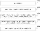
S101、提供衬底基板;S101, providing a base substrate;
S102、在衬底基板之上形成多条电源信号辅助线的图案;多条电源信号辅助线沿第二方向排列,多条电源信号辅助线中的每一条电源信号辅助线至少沿第一方向延伸,第一方向和第二方向相互交叉;S102. Form a pattern of a plurality of power signal auxiliary lines on the base substrate; the plurality of power signal auxiliary lines are arranged along the second direction, and each power signal auxiliary line in the plurality of power signal auxiliary lines extends at least along the first direction , the first direction and the second direction intersect each other;
S103、在电源信号辅助线背离衬底基板的一侧形成第一绝缘层,并采用图形化工艺形成多个露出电源信号辅助线的第一过孔;S103, forming a first insulating layer on the side of the power signal auxiliary line away from the base substrate, and using a patterning process to form a plurality of first via holes exposing the power signal auxiliary line;
S104、在第一绝缘层背离衬底基板一侧,形成多条电源信号线的图案,电源信号线通过第一过孔与电源辅助线电连接;多条电源信号线沿第一方向排列,多条电源信号线中的每一条电源信号线沿第二方向延伸;S104. Form a pattern of a plurality of power signal lines on the side of the first insulating layer away from the base substrate, and the power signal lines are electrically connected to the power supply auxiliary line through the first via hole; the plurality of power signal lines are arranged along the first direction, and the plurality of power signal lines Each of the power signal lines extends along the second direction;
S105、在电源信号线背离第一绝缘层一侧形成多个像素;其中,多个像素在第一方向和第二方向呈阵列排布,多个像素中的至少一个像素包括:子像素,以及用于驱动该像素内各子像素的像素驱动芯片;子像素包括至少一个发光器件;发光器件的第一电极与像素驱动芯片耦接,发光器件的第二电极与电源信号线耦接。S105. Form a plurality of pixels on the side where the power signal line is away from the first insulating layer; wherein, the plurality of pixels are arranged in an array in the first direction and the second direction, and at least one pixel in the plurality of pixels includes: a sub-pixel, and A pixel driving chip for driving each sub-pixel in the pixel; the sub-pixel includes at least one light emitting device; the first electrode of the light emitting device is coupled to the pixel driving chip, and the second electrode of the light emitting device is coupled to a power signal line.
本申请实施例提供的发光基板的制备方法,在衬底基板一侧形成电源辅助信号线,且每一条电源信号辅助线通过第一绝缘层的过孔与多条电源信号线中的至少部分电源信号线连接,多条电源信号辅助线以及多条电源信号线构成网格状的结构,从而可以提高与电源信号辅助线连接的电源信号线的电流均一性,提高发光器件亮度均一性,避免出现显示不均,提高显示效果。In the preparation method of the light-emitting substrate provided in the embodiment of the present application, power supply auxiliary signal lines are formed on the side of the base substrate, and each power signal auxiliary line passes through the via hole of the first insulating layer and at least part of the power supply of the plurality of power signal lines. Signal line connection, multiple power signal auxiliary lines and multiple power signal lines form a grid structure, which can improve the current uniformity of the power signal line connected to the power signal auxiliary line, improve the brightness uniformity of the light emitting device, and avoid Display unevenness, improve the display effect.
在一些实施例中,在衬底基板之上形成多条电源信号辅助线的图案的同时,还包括:In some embodiments, while forming the pattern of multiple power signal auxiliary lines on the base substrate, it also includes:
形成对位标记的图案。A pattern of alignment marks is formed.
在具体实施时,可以在衬底基板之上形成第一导电层,之后对第一导电层采用图形化工艺,形成多条电源信号辅助线的图案以及对位标记的图案。In specific implementation, a first conductive layer may be formed on the base substrate, and then a patterning process is applied to the first conductive layer to form patterns of a plurality of power signal auxiliary lines and alignment marks.
在一些实施例中,在第一绝缘层背离衬底基板一侧,形成多条电源信号线的图案的同时,还包括:In some embodiments, while forming a pattern of a plurality of power signal lines on the side of the first insulating layer away from the base substrate, it also includes:
形成多条固定电压信号线的图案、多条数据信号线的图案、以及多条选址信号线的图案。A plurality of patterns of fixed voltage signal lines, a plurality of patterns of data signal lines, and a plurality of patterns of address selection signal lines are formed.
在具体实施时,可以在第一绝缘层背离衬底基板一侧形成第二导电层,之后对第二导电层采用图形化工艺,形成多条电源信号辅助线的图案、多条固定电压信号线的图案、多条数据信号线的图案、以及多条选址信号线的图案。In specific implementation, the second conductive layer can be formed on the side of the first insulating layer away from the base substrate, and then the second conductive layer is patterned to form patterns of multiple power signal auxiliary lines and multiple fixed voltage signal lines. patterns, patterns of multiple data signal lines, and patterns of multiple address signal lines.
在一些实施例中,在电源信号线背离第一绝缘层一侧形成多个像素之前,还包括:In some embodiments, before forming a plurality of pixels on the side of the power signal line away from the first insulating layer, the method further includes:
在电源信号线背离第一绝缘层一侧形成第二绝缘层;forming a second insulating layer on the side of the power signal line away from the first insulating layer;
在第二绝缘层背离电源信号线一侧形成第三导电层,对第三导电层采用图形化工艺形成多个连接电极的图案、多条固定电压信号辅助线的图案以及多条选址信号转接线的图案;A third conductive layer is formed on the side of the second insulating layer away from the power signal line, and a patterning process is used on the third conductive layer to form a plurality of patterns of connecting electrodes, a plurality of patterns of fixed voltage signal auxiliary lines, and a plurality of address selection signal transfer lines. wiring pattern;
在连接电极背离第二绝缘层一侧依次形成第二缓冲层、第二平坦化层以及第二钝化层,并采用图形化工艺形成贯穿第二缓冲层、第二平坦化层以及第二钝化层厚度且露出第三导电层的多个第三过孔。A second buffer layer, a second planarization layer, and a second passivation layer are sequentially formed on the side of the connecting electrode away from the second insulating layer, and a second buffer layer, a second planarization layer, and a second passivation layer are formed through a patterning process. The thickness of the layer is increased and a plurality of third via holes exposing the third conductive layer.
具体实施时,在电源信号线背离第一绝缘层一侧形成第二绝缘层,具体包括:During specific implementation, the second insulating layer is formed on the side of the power signal line away from the first insulating layer, specifically including:
在电源信号线背离第一绝缘层一侧依次形成第一缓冲层和第一平坦化层,采用图形化工艺形成多个贯穿第一缓冲层和第一平坦化层的过孔;A first buffer layer and a first planarization layer are sequentially formed on the side of the power signal line away from the first insulating layer, and a plurality of via holes penetrating the first buffer layer and the first planarization layer are formed by using a patterning process;
在第一平坦化层背离第一缓冲层一侧形成第一钝化层,并对第一钝化层采用图形化工艺,在第一缓冲层和第一平坦化层的过孔区域形成露出第二导电层的过孔。Form a first passivation layer on the side of the first planarization layer away from the first buffer layer, and use a patterning process on the first passivation layer to form a first passivation layer in the via hole area of the first buffer layer and the first planarization layer to expose the first passivation layer. The via hole of the second conductive layer.
需要说明的是,图形化工艺一般包括曝光、显影等工艺。曝光工艺通常需要使用掩膜板。在一些实施例中,当第一过孔在衬底基板的正投影与第二过孔在衬底基板的正投影重合时,对第一绝缘层采用图形化工艺使用的掩膜板与对第一钝化层采用图形化工艺使用的掩膜板相同。从而可以节省掩膜板,节约成本。It should be noted that the patterning process generally includes processes such as exposure and development. The exposure process usually requires the use of a mask. In some embodiments, when the orthographic projection of the first via hole on the base substrate coincides with the orthographic projection of the second via hole on the base substrate, the mask used for the patterning process on the first insulating layer is the same as that used for the second via hole. A passivation layer adopts the same mask plate used in the patterning process. Therefore, the mask plate can be saved and the cost can be saved.
在具体实施时,露出第二导电层的过孔包括:露出第一电源信号线的第一子过孔,露出第二电源信号辅助线的第二子过孔,露出数据信号线的第四过孔,露出固定电压信号线的第五过孔和第七过孔,以及露出选址信号线的第六过孔。第三导电层通过第二绝缘层的过孔与第二导电层电连接。In specific implementation, the vias exposing the second conductive layer include: the first sub-vias exposing the first power signal line, the second sub-vias exposing the second power signal auxiliary line, and the fourth sub-vias exposing the data signal line. The fifth via hole and the seventh via hole exposing the fixed voltage signal line, and the sixth via hole exposing the address selection signal line. The third conductive layer is electrically connected to the second conductive layer through the via hole of the second insulating layer.
在具体实施时,第三过孔露出的第三导电层的区域对应焊盘区域。During specific implementation, the area of the third conductive layer exposed by the third via hole corresponds to the pad area.
在一些实施例中,形成第二钝化层之后,发光基板制备方法还包括:In some embodiments, after forming the second passivation layer, the method for preparing the light-emitting substrate further includes:
在衬底基板背离第一绝缘层一侧形成多条扇出线的图案;forming a pattern of multiple fan-out lines on the side of the base substrate away from the first insulating layer;
在衬底基板侧面形成多条侧边引线的图案;其中,侧边引线与扇出线一一对应电连接,且每一侧边引线与延伸至衬底基板边缘多条电源信号线、多条固定电压信号线、多条数据信号线、多条选址信号线中的任一条电连接。A pattern of multiple side leads is formed on the side of the base substrate; wherein, the side leads are electrically connected to the fan-out lines one by one, and each side lead is connected to a plurality of power signal lines extending to the edge of the substrate, and a plurality of fixing lines. Any one of the voltage signal line, multiple data signal lines, and multiple address signal lines is electrically connected.
在具体实施时,例如可以在衬底基板背离第一绝缘层一侧依次形成第四导电层、第五导电层以及第六导电层,并对第四导电层、第五导电层以及第六导电层采用图形化工艺形成多条扇出线的图案;之后在多条扇出线的图案背离衬底基板一侧形成第三保护层。In specific implementation, for example, the fourth conductive layer, the fifth conductive layer and the sixth conductive layer can be sequentially formed on the side of the base substrate away from the first insulating layer, and the fourth conductive layer, the fifth conductive layer and the sixth conductive layer A pattern of multiple fan-out lines is formed on the layer using a patterning process; and then a third protective layer is formed on the side of the multiple fan-out line patterns away from the substrate.
在具体实施时,第一导电层、第二导电层、第三导电层以及第五导电层的材料例如包括金属材料。金属材料例如可以是铜。第四导电层和第五导电层的材料例如包括氧化铟锡。第一平坦化层和第二平坦化层的材料例如包括树脂。其余绝缘膜层的材料例如包括氮化硅和/或氧化硅。During specific implementation, the materials of the first conductive layer, the second conductive layer, the third conductive layer and the fifth conductive layer include metal materials, for example. The metallic material may be copper, for example. The material of the fourth conductive layer and the fifth conductive layer includes, for example, indium tin oxide. The material of the first planarization layer and the second planarization layer includes resin, for example. Materials of the remaining insulating film layers include silicon nitride and/or silicon oxide, for example.
在具体实施时,在衬底基板侧面形成多条侧边引线的图案,例如可以采用溅射工艺形成侧边导电层,之后采用激光刻蚀工艺形成多条侧边引线的图案。再之后可以涂覆覆盖侧边引线的保护油墨。In specific implementation, a plurality of side lead patterns are formed on the side of the base substrate, for example, a sputtering process may be used to form a side conductive layer, and then a laser etching process is used to form a plurality of side lead patterns. A protective ink covering the side leads can then be applied afterwards.
本申请实施例提供的发光基板的制备方法,即便在形成侧边引线的工艺中出现部分侧边引线受损,导致侧边引线的电阻出现异常,进而在发光基板驱动过程中导致与电阻出现异常的侧边引线电连接的电源信号线的电流出现异常,由于多条电源信号辅助线以及多条电源信号线构成网格状的结构,可以对电流出现异常的电源信号线进行补偿,从而可以避免由于侧边引线电阻不均造成的多条电源信号线的电流均一性差,避免出现显示不均,提高显示效果。In the preparation method of the light-emitting substrate provided in the embodiment of the present application, even if part of the side leads are damaged during the process of forming the side leads, the resistance of the side leads is abnormal, which in turn leads to an abnormality in the resistance of the light-emitting substrate during the driving process. The current of the power signal line electrically connected to the side lead of the side lead is abnormal. Since multiple power signal auxiliary lines and multiple power signal lines form a grid structure, the power signal line with abnormal current can be compensated, thereby avoiding The current uniformity of multiple power signal lines caused by the uneven resistance of the side lead wires can avoid uneven display and improve the display effect.
在一些实施例中,在电源信号线背离第一绝缘层一侧形成多个像素,具体包括:In some embodiments, a plurality of pixels are formed on the side of the power signal line away from the first insulating layer, specifically including:
在第二钝化层背离衬底基板一侧绑定发光器件以及像素驱动芯片。A light-emitting device and a pixel driving chip are bonded on the side of the second passivation layer away from the substrate.
在具体实施时,发光器件的第一电极和第二电极分别和与其对应的焊盘绑定,像素驱动芯片的各信号端分别和预期对应的焊盘绑定。发光器件与焊盘绑定以及像素驱动芯片与焊盘绑定参见发光基板实施例部分,在此不再赘述。In a specific implementation, the first electrode and the second electrode of the light emitting device are respectively bound to corresponding pads, and each signal terminal of the pixel driving chip is respectively bound to expected corresponding pads. For the binding of the light-emitting device and the bonding pad and the binding of the pixel driving chip and the bonding pad, refer to the part of the embodiment of the light-emitting substrate, which will not be repeated here.
本申请实施例提供的一种显示装置,包括:本申请实施例提供的上述发光基板。A display device provided in an embodiment of the present application includes: the above light-emitting substrate provided in the embodiment of the present application.
在一些实施例中,显示装置由多个本申请实施例提供的上述发光基板拼接形成。In some embodiments, the display device is formed by splicing the above-mentioned light-emitting substrates provided by the embodiments of the present application.
本申请实施例提供的显示装置为:手机、平板电脑、电视机、显示器、笔记本电脑、数码相框、导航仪等任何具有显示功能的产品或部件。对于该显示装置的其它必不可少的组成部分均为本领域的普通技术人员应该理解具有的,在此不做赘述,也不应作为对本申请的限制。该显示装置的实施可以参见上述发光基板的实施例,重复之处不再赘述。The display device provided in the embodiment of the present application is any product or component with a display function such as a mobile phone, a tablet computer, a television, a monitor, a notebook computer, a digital photo frame, a navigator, and the like. The other essential components of the display device should be understood by those of ordinary skill in the art, and will not be repeated here, nor should they be used as limitations on the present application. For the implementation of the display device, reference may be made to the above-mentioned embodiments of the light-emitting substrate, and repeated descriptions will not be repeated.
综上所述,本申请实施例提供的发光基板及其制备方法、显示装置,每一条电源信号辅助线与多条电源信号线中的至少部分电源信号线连接,多条电源信号辅助线以及多条电源信号线构成网格状的结构,从而可以提高与电源信号辅助线连接的电源信号线的电流均一性,提高发光器件亮度均一性。当本申请实施例提供的发光基板应用于拼接显示产品、且电源信号线需要通过侧边引线引出至背面,即便部分侧边引线的电阻出现异常,导致侧边引线电阻不均,进而导致与电阻出现异常的侧边引线电连接的电源信号线的电流出现异常,由于多条电源信号辅助线以及多条电源信号线构成网格状的结构,可以对电流出现异常的电源信号线进行补偿,从而可以避免由于侧边引线电阻不均造成的多条电源信号线的电流均一性差,避免出现显示不均,提高显示效果。To sum up, in the light-emitting substrate and its preparation method and display device provided by the embodiments of the present application, each power signal auxiliary line is connected to at least part of the power signal lines among the multiple power signal lines, and the multiple power signal auxiliary lines and the multiple power signal lines are connected to each other. The power signal lines form a grid-like structure, so that the current uniformity of the power signal lines connected to the power signal auxiliary lines can be improved, and the brightness uniformity of the light emitting device can be improved. When the light-emitting substrate provided by the embodiment of the present application is applied to a splicing display product, and the power signal line needs to be led out to the back through the side leads, even if the resistance of some side leads is abnormal, resulting in uneven resistance of the side leads, which in turn leads to The current of the power signal line electrically connected to the abnormal side lead wire is abnormal. Since multiple power signal auxiliary lines and multiple power signal lines form a grid structure, the power signal line with abnormal current can be compensated, thereby It can avoid poor current uniformity of multiple power signal lines caused by uneven resistance of side lead wires, avoid uneven display, and improve display effect.
显然,本领域的技术人员可以对本申请进行各种改动和变型而不脱离本申请的精神和范围。这样,倘若本申请的这些修改和变型属于本申请权利要求及其等同技术的范围之内,则本申请也意图包含这些改动和变型在内。Obviously, those skilled in the art can make various changes and modifications to the application without departing from the spirit and scope of the application. In this way, if these modifications and variations of the present application fall within the scope of the claims of the present application and their equivalent technologies, the present application is also intended to include these modifications and variations.
Claims (11)
Priority Applications (1)
| Application Number | Priority Date | Filing Date | Title |
|---|---|---|---|
| CN202110409330.6ACN113130463B (en) | 2021-04-16 | 2021-04-16 | A light-emitting substrate, its preparation method, and a display device |
Applications Claiming Priority (1)
| Application Number | Priority Date | Filing Date | Title |
|---|---|---|---|
| CN202110409330.6ACN113130463B (en) | 2021-04-16 | 2021-04-16 | A light-emitting substrate, its preparation method, and a display device |
Publications (2)
| Publication Number | Publication Date |
|---|---|
| CN113130463A CN113130463A (en) | 2021-07-16 |
| CN113130463Btrue CN113130463B (en) | 2022-12-02 |
Family
ID=76777428
Family Applications (1)
| Application Number | Title | Priority Date | Filing Date |
|---|---|---|---|
| CN202110409330.6AActiveCN113130463B (en) | 2021-04-16 | 2021-04-16 | A light-emitting substrate, its preparation method, and a display device |
Country Status (1)
| Country | Link |
|---|---|
| CN (1) | CN113130463B (en) |
Families Citing this family (10)
| Publication number | Priority date | Publication date | Assignee | Title |
|---|---|---|---|---|
| US12272779B2 (en) | 2021-09-02 | 2025-04-08 | Hefei Xinsheng Optoelectronics Technology Co., Ltd. | Wiring substrate, display substrate and display apparatus |
| WO2023050209A1 (en)* | 2021-09-29 | 2023-04-06 | 京东方科技集团股份有限公司 | Light-emitting substrate and display apparatus |
| WO2023050378A1 (en)* | 2021-09-30 | 2023-04-06 | 京东方科技集团股份有限公司 | Light-emitting substrate, backlight module, and display device |
| US20240258478A1 (en)* | 2021-10-27 | 2024-08-01 | Hefei BOE Ruisheng Technology Co., Ltd. | Light-emitting substrate, method for manufacturing the same, and display device |
| CN116391221A (en)* | 2021-11-02 | 2023-07-04 | 京东方科技集团股份有限公司 | Light-emitting substrate and display device |
| CN114171546A (en)* | 2021-12-02 | 2022-03-11 | Tcl华星光电技术有限公司 | MiniLED backlight substrate, display panel and display device |
| CN116264233A (en)* | 2021-12-15 | 2023-06-16 | 合肥京东方瑞晟科技有限公司 | LED driving backboard and display device |
| US12230189B2 (en)* | 2022-04-24 | 2025-02-18 | BOE MLED Technology Co., Ltd. | Electronic device and display driving method |
| CN115084185B (en)* | 2022-07-15 | 2025-08-22 | Tcl华星光电技术有限公司 | Light-emitting substrate and display device |
| CN116013196B (en)* | 2022-12-27 | 2024-06-18 | 深圳市华星光电半导体显示技术有限公司 | Display panel |
Family Cites Families (6)
| Publication number | Priority date | Publication date | Assignee | Title |
|---|---|---|---|---|
| KR101871420B1 (en)* | 2012-02-08 | 2018-06-28 | 삼성디스플레이 주식회사 | Organic Light Emitting Display device |
| CN103345092B (en)* | 2013-07-08 | 2017-03-29 | 合肥京东方光电科技有限公司 | Array base palte and preparation method thereof, display device |
| CN109087922B (en)* | 2018-09-19 | 2020-09-29 | 合肥鑫晟光电科技有限公司 | Array substrate and manufacturing method thereof, and display panel |
| CN112185267B (en)* | 2019-06-12 | 2022-03-29 | 云谷(固安)科技有限公司 | Circuit substrate, display panel and display device |
| CN113228291B (en)* | 2019-09-27 | 2024-03-05 | 京东方科技集团股份有限公司 | Array substrate, display device, manufacturing method of array substrate, and pixel drive circuit |
| CN211654192U (en)* | 2020-05-13 | 2020-10-09 | 京东方科技集团股份有限公司 | Array substrate and splicing display panel |
- 2021
- 2021-04-16CNCN202110409330.6Apatent/CN113130463B/enactiveActive
Also Published As
| Publication number | Publication date |
|---|---|
| CN113130463A (en) | 2021-07-16 |
Similar Documents
| Publication | Publication Date | Title |
|---|---|---|
| CN113130463B (en) | A light-emitting substrate, its preparation method, and a display device | |
| CN111524928B (en) | Display panel and display device | |
| CN110211987B (en) | LED panel | |
| US12334426B2 (en) | Array substrate, display panel and display module | |
| CN115188792A (en) | Display substrate and display device | |
| CN108241240A (en) | Display panel and display device | |
| CN103383512B (en) | Liquid crystal disply device and its preparation method | |
| TWI751857B (en) | Light-emitting substrate and display device | |
| CN109725447B (en) | Array substrate, display panel and display device | |
| US10262563B2 (en) | LED display | |
| CN114793473B (en) | Light-emitting substrate, preparation method thereof and array substrate | |
| CN114333615B (en) | Substrate mother board and its preparation method, driving substrate and display device | |
| CN217506872U (en) | Display panel, display screen and electronic equipment | |
| US20240404959A1 (en) | Wiring substrate, array substrate and light emitting module having control regions arranged into control region rows and control region columns | |
| TW202129958A (en) | Light emitting plate, circuit board, and display device | |
| CN116322183A (en) | Display panel and display device | |
| WO2021146958A1 (en) | Light-emitting plate, circuit board and display apparatus | |
| CN117241644A (en) | Display panel and display device | |
| CN113867043B (en) | Light-emitting substrate, manufacturing method thereof, and display device | |
| WO2023005610A1 (en) | Drive substrate and preparation method therefor, and light-emitting apparatus | |
| CN115411082A (en) | Display panel and display device | |
| CN115605938A (en) | Light emitting substrate, display device, and method of driving light emitting substrate | |
| CN115552626B (en) | Display substrate and display device | |
| EP4345864A1 (en) | Light-emitting substrate and display device | |
| US12118922B2 (en) | Display apparatus |
Legal Events
| Date | Code | Title | Description |
|---|---|---|---|
| PB01 | Publication | ||
| PB01 | Publication | ||
| SE01 | Entry into force of request for substantive examination | ||
| SE01 | Entry into force of request for substantive examination | ||
| GR01 | Patent grant | ||
| GR01 | Patent grant |