CN113114174A - Broadband orthogonal signal generator and signal generating method - Google Patents
Broadband orthogonal signal generator and signal generating methodDownload PDFInfo
- Publication number
- CN113114174A CN113114174ACN202110556642.XACN202110556642ACN113114174ACN 113114174 ACN113114174 ACN 113114174ACN 202110556642 ACN202110556642 ACN 202110556642ACN 113114174 ACN113114174 ACN 113114174A
- Authority
- CN
- China
- Prior art keywords
- signal
- output
- voltage
- phase
- cpu
- Prior art date
- Legal status (The legal status is an assumption and is not a legal conclusion. Google has not performed a legal analysis and makes no representation as to the accuracy of the status listed.)
- Granted
Links
- 238000000034methodMethods0.000titleclaimsabstractdescription22
- 238000006243chemical reactionMethods0.000claimsdescription9
- 230000010363phase shiftEffects0.000claimsdescription8
- 238000001514detection methodMethods0.000claimsdescription6
- 230000007274generation of a signal involved in cell-cell signalingEffects0.000claimsdescription3
- 238000003199nucleic acid amplification methodMethods0.000claimsdescription3
- 230000003247decreasing effectEffects0.000claims4
- 230000010354integrationEffects0.000claims1
- 230000001105regulatory effectEffects0.000claims1
- 230000007423decreaseEffects0.000description15
- 230000008859changeEffects0.000description4
- 238000004891communicationMethods0.000description3
- 238000005516engineering processMethods0.000description3
- 230000003321amplificationEffects0.000description2
- 238000010586diagramMethods0.000description2
- 230000006870functionEffects0.000description2
- 238000012986modificationMethods0.000description2
- 230000004048modificationEffects0.000description2
- 230000009286beneficial effectEffects0.000description1
- 230000005540biological transmissionEffects0.000description1
- 238000005259measurementMethods0.000description1
- 238000012360testing methodMethods0.000description1
Images


Classifications
- H—ELECTRICITY
- H03—ELECTRONIC CIRCUITRY
- H03K—PULSE TECHNIQUE
- H03K5/00—Manipulating of pulses not covered by one of the other main groups of this subclass
Landscapes
- Physics & Mathematics (AREA)
- Nonlinear Science (AREA)
- Stabilization Of Oscillater, Synchronisation, Frequency Synthesizers (AREA)
Abstract
Description
Translated fromChinese技术领域technical field
本发明涉及一种宽频正交信号发生器及信号发生方法,属于信号发生器技术领域。The invention relates to a broadband quadrature signal generator and a signal generating method, and belongs to the technical field of signal generators.
背景技术Background technique
在现代通信及测试仪器中,经常会应用正交信号源完成信号调制、解调等功能。现有正交信号发生器产生正交的方法有以下几种,即:使用移相器、二分频器及DDS技术。In modern communication and test instruments, quadrature signal sources are often used to complete functions such as signal modulation and demodulation. There are several methods for generating quadrature in the existing quadrature signal generator, namely: using a phase shifter, a two-frequency divider and DDS technology.
现有技术中的移相器通常采用RC移相或RL移相电路组成,该方法通常只能对单一频率信号产生正交信号输出。The phase shifter in the prior art is usually composed of an RC phase shift or RL phase shift circuit, and this method can usually only generate a quadrature signal output for a single frequency signal.
二分频器法通过数字电路产生非正弦正交信号,该方法应用范围窄,且由于数字电路的工作频率较低,不适用于宽频或高频正交信号输出。The divide-by-two method generates a non-sinusoidal quadrature signal through a digital circuit. This method has a narrow application range and is not suitable for broadband or high-frequency quadrature signal output due to the low operating frequency of the digital circuit.
DDS技术产生正交信号是近年来的主流方法,该方法通过数字技术产生正弦正交信号,但是,该方法高频噪声大,无法产生较高频率的正交信号,且该方法在宽频范围内变化时,由于宽频正交信号在传输过程中会由于电路参数的不一致,导致输出信号不能严格正交。现有电路调节方法只能对单一频率的高频信号进行正交相位补偿,对于频率可变的高频信号无法进行正交补偿。无法保证输出信号的严格正交。DDS technology to generate quadrature signals is the mainstream method in recent years. This method generates sinusoidal quadrature signals through digital technology. However, this method has large high-frequency noise and cannot generate higher frequency quadrature signals, and this method is in a wide frequency range. When changing, the output signal cannot be strictly orthogonal due to inconsistent circuit parameters in the transmission process of the broadband quadrature signal. The existing circuit adjustment method can only perform quadrature phase compensation for high-frequency signals of a single frequency, but cannot perform quadrature compensation for high-frequency signals with variable frequencies. Strict quadrature of the output signals cannot be guaranteed.
专利“宽带正交信号产生器(ZL 201210191427.5)”通过移相器及I路幅度调节器、Q路幅度调节器产生正交信号的方法,该方法采用较复杂的幅度调节器实现正交信号调节,电路结构复杂。The patent "Broadband Quadrature Signal Generator (ZL 201210191427.5)" uses a phase shifter, an I-channel amplitude regulator, and a Q-channel amplitude regulator to generate a quadrature signal. This method uses a more complex amplitude regulator to achieve quadrature signal adjustment , the circuit structure is complex.
为了解决上述突出的问题,本领域技术人员急需要提出一种新的宽频正交信号发生器。In order to solve the above outstanding problems, those skilled in the art urgently need to propose a new broadband quadrature signal generator.
发明内容SUMMARY OF THE INVENTION
目的:为了克服现有技术中存在的无法实现频率在较大范围内变化时输出信号不能严格正交的问题,本发明提供一种宽频正交信号发生器及信号发生方法,弥补了通信及测量领域的技术要求。Purpose: In order to overcome the problem in the prior art that the output signal cannot be strictly orthogonal when the frequency changes within a large range, the present invention provides a broadband orthogonal signal generator and a signal generation method, which makes up for the communication and measurement. technical requirements in the field.
技术方案:为解决上述技术问题,本发明采用的技术方案为:Technical scheme: in order to solve the above-mentioned technical problems, the technical scheme adopted in the present invention is:
一种宽频正交信号发生器,包括如下模块:A broadband quadrature signal generator, comprising the following modules:
微分电路用于将原信号vs进行移相,得到输出信号vD。The differentiating circuit is used to shift the phase of the original signal vs to obtain the output signal vD .
积分电路用于将原信号vs进行移相,得到输出信号vI。The integrating circuit is used to shift the phase of the original signal vs to obtain the output signal vI .
第一D/A模块用于将CPU输出的第一电压信号转换为直流电压。The first D/A module is used to convert the first voltage signal output by the CPU into a DC voltage.
第二D/A模块用于将CPU输出的第二电压信号转换为直流电压。The second D/A module is used for converting the second voltage signal output by the CPU into a DC voltage.
第一放大器用于隔离放大第一D/A模块输出的直流电压,输出电压为K1。The first amplifier is used for isolating and amplifying the DC voltage output by the first D/A module, and the output voltage is K1 .
第二放大器用于隔离放大第二D/A模块输出的直流电压,输出电压为K2。The second amplifier is used for isolating and amplifying the DC voltage output by the second D/A module, and the output voltage is K2 .
第一乘法器用于将直流电压K1与输出信号vI相乘,得到输出信号K1·vI。The first multiplier is used to multiply the DC voltage K1 by the output signal vI to obtain the output signal K1 ·vI .
第二乘法器用于将直流电压K2与输出信号vD相乘,得到输出信号K2·vD。The second multiplier is used to multiply the DC voltage K2 by the output signal vD to obtain the output signal K2 ·vD .
第一加法器用于将输出信号vI与输出信号K2·vD进行叠加,输出信号为v0。The first adder is used to superimpose the output signal vI and the output signal K2 ·vD , and the output signal is v0 .
第二加法器用于将输出信号vD与输出信号K1·vI进行叠加,输出信号为v90。The second adder is used to superimpose the output signal vD and the output signal K1 ·vI , and the output signal is v90 .
正交误差检测模块用于将输出信号v0与输出信号v90的相位差与90°做比较,如果相等,输出信号Vd=0,如果不相等,输出信号Vd>0,且两者差值越大,Vd值越大。The quadrature error detection module is used to compare the phase difference between the output signal v0 and the output signal v90 with 90°, if they are equal, the output signal Vd =0, if they are not equal, the output signal Vd >0, and the two The larger the difference, the larger theVd value.
CPU用于当Vd=0时,CPU保持当前时刻第一电压信号、第二电压信号的输出。The CPU is used for maintaining the output of the first voltage signal and the second voltage signal at the current moment when Vd =0.
当Vd>0时,CPU增加第一电压信号作为输出,保持第二电压信号的输出不变,判断下一时刻Vd相较上一时刻Vd是增加还是减少,如Vd是减少,继续增加第一电压信号作为输出,直到Vd=0;如Vd是增加,CPU停止调节第一电压信号,保持当前时刻第一电压信号的输出不变,持继减少第二电压信号作为输出,直到Vd=0。When Vd > 0, the CPU increases the first voltage signal as output, keeps the output of the second voltage signal unchanged, and judges whether Vd at the next moment increases or decreases compared to the previous moment Vd , such as Vd decreases, Continue to increase the first voltage signal as output until Vd = 0; if Vd increases, the CPU stops adjusting the first voltage signal, keeps the output of the first voltage signal at the current moment unchanged, and continues to reduce the second voltage signal as output , until Vd =0.
作为优选方案,还包括高频信号源,高频信号源用于产生频率可变的原信号vs。As a preferred solution, a high-frequency signal source is also included, and the high-frequency signal source is used to generate the original signal vs with variable frequency.
作为优选方案,正交误差检测模块包括:鉴相器、第三放大器、A/D转换电路;所述鉴相器用于将输出信号v0与输出信号v90的相位差与90°做比较,如果相等,输出电压=0,如果不相等,输出电压>0,且两者差值越大,电压值越大。As a preferred solution, the quadrature error detection module includes: a phase detector, a third amplifier, and an A/D conversion circuit; the phase detector is used to compare the phase difference between the output signal v0 and the output signal v90 with 90°, If they are equal, the output voltage = 0, if they are not equal, the output voltage is > 0, and the greater the difference between the two, the greater the voltage value.
第三放大器用于放大鉴相器输出电压。The third amplifier is used to amplify the output voltage of the phase detector.
A/D转换电路用于将放大后的鉴相器输出电压转换为数字信号Vd并送到CPU。The A/D conversion circuit is used to convert the amplified output voltage of the phase detector into a digital signal Vd and send it to the CPU.
作为优选方案,所述原信号vs为正弦交流信号。As a preferred solution, the original signal vs is a sinusoidal AC signal.
作为优选方案,输出信号vD的移相结果是


一种宽频正交信号发生方法,包括如下步骤:A method for generating a broadband quadrature signal, comprising the following steps:
调节高频信号源,使其输出频率为f0的原信号vs。Adjust the high frequency signal source so that it outputs the original signal vs of frequency f0 .
将原信号vs分别进行移相,得到输出信号vD、vI。Phase-shift the original signal vs respectively to obtain the output signals vD and vI .
CPU输出第一电压信号、第二电压信号,经数模转换、放大后得到直流电压为K1、K2。The CPU outputs the first voltage signal and the second voltage signal, and after digital-to-analog conversion and amplification, the DC voltages are obtained as K1 and K2 .
将信号vI与直流电压K1相乘,得到信号K1·vI。The signal vI is multiplied by the DC voltage K1 to obtain the signal K1 ·vI .
将信号vD与直流电压K2相乘,得到信号K2·vD。The signal vD is multiplied by the DC voltage K2 to obtain the signal K2 ·vD .
将信号vI与信号K2·vD进行相加,得到信号v0。The signal vI is added to the signal K2 ·vD to obtain the signal v0 .
将信号vD与信号K1·vI进行相加,得到信号v90。The signal vD is added to the signal K1 ·vI to obtain the signal v90 .
将信号v0与信号v90的相位差与90°做比较,如果相等,输出信号Vd=0,如果不相等,输出信号Vd>0,且两者差值越大,Vd值越大。Compare the phase difference between the signal v0 and the signal v90 with 90°, if they are equal, the output signal Vd = 0, if not, the output signal Vd > 0, and the greater the difference between the two, the greater the Vd value. big.
当Vd=0时,CPU保持当前时刻第一电压信号、第二电压信号的输出。When Vd =0, the CPU keeps the output of the first voltage signal and the second voltage signal at the current moment.
当Vd>0时,CPU增加第一电压信号作为输出,保持第二电压信号的输出不变,判断下一时刻Vd相较上一时刻Vd是增加还是减少,如Vd是减少,继续增加第一电压信号作为输出,直到Vd=0;如Vd是增加,CPU停止调节第一电压信号,保持当前时刻第一电压信号的输出不变,持继减少第二电压信号作为输出,直到Vd=0。When Vd > 0, the CPU increases the first voltage signal as output, keeps the output of the second voltage signal unchanged, and judges whether Vd at the next moment increases or decreases compared to the previous moment Vd , such as Vd decreases, Continue to increase the first voltage signal as output until Vd = 0; if Vd increases, the CPU stops adjusting the first voltage signal, keeps the output of the first voltage signal at the current moment unchanged, and continues to reduce the second voltage signal as output , until Vd =0.
作为优选方案,当Vd=0时,CPU保存下各输出频率f0对应的第一电压信号、第二电压信号、直流电压K1、K2。As a preferred solution, when Vd =0, the CPU saves the first voltage signal, the second voltage signal, and the DC voltages K1 and K2 corresponding to each output frequency f0 .
有益效果:本发明提供的一种宽频正交信号发生器及信号发生方法,本发明可以在频率较大范围内变化时,始终保持输出信号处于正交状态,满足通信系统及仪器仪表等系统的要求。与现有技术相比,应用该电路结构,使得输出正交信号相位误差小;其利用CPU进行实时相位补偿,能实现在宽频范围内达到正交输出。Beneficial effects: the invention provides a broadband quadrature signal generator and a signal generation method, the invention can always keep the output signal in a quadrature state when the frequency changes within a large range, which satisfies the requirements of communication systems, instruments and other systems. Require. Compared with the prior art, the application of the circuit structure makes the phase error of the output quadrature signal small; the real-time phase compensation is performed by the CPU, and the quadrature output can be achieved in a wide frequency range.
附图说明Description of drawings
图1为本发明宽频正交信号发生器的框图。FIG. 1 is a block diagram of a broadband quadrature signal generator of the present invention.
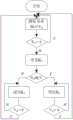
图2为本发明宽步正交信号发生器CPU正交补偿流程图。FIG. 2 is a flowchart of the CPU quadrature compensation of the wide-step quadrature signal generator according to the present invention.
图3为本发明宽频正交信号发生器正交调节相量图。FIG. 3 is a diagram of the quadrature adjustment phasor of the broadband quadrature signal generator of the present invention.
具体实施方式Detailed ways
下面结合具体实施例对本发明作更进一步的说明。The present invention will be further described below in conjunction with specific embodiments.
如图1所示,一种宽频正交信号发生器,包括如下模块:As shown in Figure 1, a broadband quadrature signal generator includes the following modules:
高频信号源用于产生频率可变的正弦交流信号:A high-frequency signal source is used to generate a sinusoidal AC signal with variable frequency:

式中:vs为高频信号源输出信号,Vm为信号源电压最大值;f为信号源产生的交流信号频率,该频率可变;
微分电路用于将高频信号源产生的正弦信号进行移相,输出信号为:The differential circuit is used to shift the phase of the sinusoidal signal generated by the high-frequency signal source, and the output signal is:

其中,vD为微分电路输出信号,VDm为微分电路输出信号电压最大值,
合理选择微分电路元件,使:Reasonable selection of differential circuit components makes:

积分电路用于将高频信号源产生的正弦信号进行移相,输出信号为:The integrating circuit is used to phase-shift the sinusoidal signal generated by the high-frequency signal source, and the output signal is:

其中,vI为积分电路输出信号,VIm为积分电路输出信号电压最大值,
合理选择积分电路元件,使:Reasonable selection of integrator circuit components makes:

通过微分电路与积分电路的移相,使微分电路输出信号与积分电路输出信号的相位差大于90°,由于:Through the phase shift between the differential circuit and the integrating circuit, the phase difference between the output signal of the differential circuit and the output signal of the integrating circuit is greater than 90°, because:


所以有:F:

第一放大器用于隔离放大第一D/A模块输出的直流电压,输出电压为K1。The first amplifier is used for isolating and amplifying the DC voltage output by the first D/A module, and the output voltage is K1 .
第二放大器用于隔离放大第二D/A模块输出的直流电压,输出电压为K2。The second amplifier is used for isolating and amplifying the DC voltage output by the second D/A module, and the output voltage is K2 .
第一乘法器用于将第一放大器输出的直流电压K1与积分电路的输出信号vI相乘,改变积分电路输出信号幅度,其输出信号为:The first multiplier is used to multiply the DC voltage K1 output by the first amplifier and the output signal vI of the integrating circuit to change the amplitude of the output signal of the integrating circuit. The output signal is:

第二乘法器用于将第二放大器输出的直流电压K2与微分电路的输出信号vD相乘,改变微分电路输出信号幅度,其输出信号为:The second multiplier is used to multiply the DC voltage K2 output by the second amplifier with the output signal vD of the differential circuit, and change the amplitude of the output signal of the differential circuit. The output signal is:

第一加法器用于将积分电路的输出信号vI与第二乘法器输出信号K2·vD进行叠加,输出信号为v0,用于改变输出信号v0的相位;即:The first adder is used to superimpose the output signal vI of the integrating circuit and the output signal K2 ·vD of the second multiplier, and the output signal is v0 , which is used to change the phase of the output signal v0 ; namely:

第二加法器用于将微分电路的输出信号vD与第一乘法器输出信号K1·vI进行相量叠加,输出信号v90,用于改变输出信号的v90相位,即:The second adder is used for phasor superposition of the output signal vD of the differential circuit and the output signal K1 ·vI of the first multiplier, and the output signal v90 is used to change the phase of v90 of the output signal, namely:

鉴相器用于对v0、v90的正交误差进行检测,当完全正交时,鉴相器输出检测直流电压为0,当存在正交误差时,鉴相器输出检测直流电压大于0,从而实现正交误差检测功能。The phase detector is used to detect the quadrature errors of v0 and v90 . When it is completely quadrature, the detected DC voltage of the phase detector output is 0. When there is a quadrature error, the detected DC voltage of the phase detector output is greater than 0. Thus, the quadrature error detection function is realized.
第三放大器用于放大鉴相后的检测直流电压,并将放大后的信号送到A/D转换电路。The third amplifier is used to amplify the detected DC voltage after phase discrimination, and send the amplified signal to the A/D conversion circuit.
A/D转换电路用于将放大后的检测直流电压转换为数字信号Vd并送到CPU;The A/D conversion circuit is used to convert the amplified detection DC voltage into a digital signal Vd and send it to the CPU;
第一D/A模块用于将CPU输出的第一电压信号转换为直流电压。The first D/A module is used to convert the first voltage signal output by the CPU into a DC voltage.
第二D/A模块用于将CPU输出的第二电压信号转换为直流电压。The second D/A module is used for converting the second voltage signal output by the CPU into a DC voltage.
如图2所示,CPU用于调节v0、v90的相位

当Vd=0时,CPU保持当前时刻第一电压信号、第二电压信号的输出。When Vd =0, the CPU keeps the output of the first voltage signal and the second voltage signal at the current moment.
当Vd>0时,CPU增加第一电压信号作为输出,保持第二电压信号的输出不变,判断下一时刻Vd相较上一时刻Vd是增加还是减少,如Vd是减少,继续增加第一电压信号作为输出,使Vd进一步减少,直到Vd=0;如Vd是增加,CPU停止调节第一电压信号,保持当前时刻第一电压信号的输出不变,持继减少第二电压信号作为输出,使Vd进一步减少,直到Vd=0。When Vd > 0, the CPU increases the first voltage signal as output, keeps the output of the second voltage signal unchanged, and judges whether Vd at the next moment increases or decreases compared to the previous moment Vd , such as Vd decreases, Continue to increase the first voltage signal as the output to further decrease Vd until Vd =0; if Vd increases, the CPU stops adjusting the first voltage signal, keeps the output of the first voltage signal at the current moment unchanged, and continues to decrease The output of the second voltage signal further reduces Vd until Vd =0.
如图3所示,将正弦交流信号vI、vD用相量表示,即:


实施例1:Example 1:
在对本发明的正交信号发生器进行调试时,将高频信号源的频率从低往高调节,用鉴相器对最终输出信号的正交性进行检测,再通过CPU改变K1、K2的值,使最终输出信号严格正交,CPU同时将各频率点的输出电压信号数字量记录在存储器中。在正交信号发生器工作时,根据高频信号源实时输出的信号频率,用记录好的输出电压信号数字量产生该频率点所需的K1、K2电压,从而使输出信号保持在宽频范围内的严格正交。When debugging the quadrature signal generator of the present invention, the frequency of the high-frequency signal source is adjusted from low to high, the quadrature of the final output signal is detected by a phase detector, and K1 and K2 are changed by the CPU. The value of , so that the final output signal is strictly orthogonal, and the CPU simultaneously records the digital quantity of the output voltage signal at each frequency point in the memory. When the quadrature signal generator is working, according to the real-time output signal frequency of the high-frequency signal source, the digital quantity of the recorded output voltage signal is used to generate the K1 and K2 voltages required for the frequency point, so as to keep the output signal at a wide frequency Strictly orthogonal in the range.
实施例2:Embodiment 2:
一种宽频正交信号发生方法,以频率点f0信号作正交补偿调节为例说明。A method for generating a broadband quadrature signal is illustrated by taking the frequency point f0 signal for quadrature compensation adjustment as an example.
本实施例提供的高频信号源在f0频率点进行信号输入,宽频正交信号发生器对输入的信号进行正交信号补偿,使输出信号处于正交状态。具体包括如下步骤:The high-frequency signal source provided in this embodiment performs signal input at the f0 frequency point, and the broadband quadrature signal generator performs quadrature signal compensation on the input signal, so that the output signal is in a quadrature state. Specifically include the following steps:
调节高频信号源,使其输出频率为f0的正弦信号,设该信号为:Adjust the high-frequency signal source to output a sinusoidal signal with a frequency of f0 , and set the signal to be:

式中:Vsm为高频正弦交流电压的最大值,
将正弦信号分别进行移相,其输出信号为:The sinusoidal signals are phase-shifted respectively, and the output signal is:


式中:vIm为积分电路输出信号的最大值、vDm为微分电路输出信号的最大值、

CPU输出第一电压信号、第二电压信号,经数模转换、放大后得到直流电压为K1、K2。The CPU outputs the first voltage signal and the second voltage signal, and after digital-to-analog conversion and amplification, the DC voltages are obtained as K1 and K2 .
将信号vI与直流电压K1相乘,其输出信号为:Multiplying the signal vI by the DC voltage K1 , the output signal is:

将信号vD与直流电压K2相乘,其输出信号为:Multiplying the signalvD by the DC voltage K2, the output signal is:

将信号vC2与信号vI相加,得到输出信号为:Adding the signal vC2 to the signal vI , the output signal is:

将该表达式用相量进行表示,即:Express this expression in terms of a phasor, that is:

将信号vC1与信号vD相加,得到输出信号为:Adding the signal vC1 to the signal vD , the output signal is:

将该表达式用相量进行表示,即:Express this expression in terms of a phasor, that is:

根据v0、v90的正交误差Vd调节v0、v90的相位
当Vd=0时,CPU保持当前时刻第一电压信号、第二电压信号的输出。When Vd =0, the CPU keeps the output of the first voltage signal and the second voltage signal at the current moment.
当Vd>0时,CPU增加第一电压信号作为输出,保持第二电压信号的输出不变,判断下一时刻Vd相较上一时刻Vd是增加还是减少,如Vd是减少,继续增加第一电压信号作为输出,使Vd进一步减少,直到Vd=0;如Vd是增加,CPU停止调节第一电压信号,保持当前时刻第一电压信号的输出不变,持继减少第二电压信号作为输出,使Vd进一步减少,直到Vd=0。When Vd > 0, the CPU increases the first voltage signal as output, keeps the output of the second voltage signal unchanged, and judges whether Vd at the next moment increases or decreases compared to the previous moment Vd , such as Vd decreases, Continue to increase the first voltage signal as the output to further decrease Vd until Vd =0; if Vd increases, the CPU stops adjusting the first voltage signal, keeps the output of the first voltage signal at the current moment unchanged, and continues to decrease The output of the second voltage signal further reduces Vd until Vd =0.
以上所述仅是本发明的优选实施方式,应当指出:对于本技术领域的普通技术人员来说,在不脱离本发明原理的前提下,还可以做出若干改进和润饰,这些改进和润饰也应视为本发明的保护范围。The above is only the preferred embodiment of the present invention, it should be pointed out: for those skilled in the art, under the premise of not departing from the principle of the present invention, several improvements and modifications can also be made, and these improvements and modifications are also It should be regarded as the protection scope of the present invention.
Claims (7)


Priority Applications (1)
| Application Number | Priority Date | Filing Date | Title |
|---|---|---|---|
| CN202110556642.XACN113114174B (en) | 2021-05-21 | 2021-05-21 | A wideband orthogonal signal generator and signal generation method |
Applications Claiming Priority (1)
| Application Number | Priority Date | Filing Date | Title |
|---|---|---|---|
| CN202110556642.XACN113114174B (en) | 2021-05-21 | 2021-05-21 | A wideband orthogonal signal generator and signal generation method |
Publications (2)
| Publication Number | Publication Date |
|---|---|
| CN113114174Atrue CN113114174A (en) | 2021-07-13 |
| CN113114174B CN113114174B (en) | 2023-09-26 |
Family
ID=76722882
Family Applications (1)
| Application Number | Title | Priority Date | Filing Date |
|---|---|---|---|
| CN202110556642.XAActiveCN113114174B (en) | 2021-05-21 | 2021-05-21 | A wideband orthogonal signal generator and signal generation method |
Country Status (1)
| Country | Link |
|---|---|
| CN (1) | CN113114174B (en) |
Citations (9)
| Publication number | Priority date | Publication date | Assignee | Title |
|---|---|---|---|---|
| CN1101180A (en)* | 1993-08-10 | 1995-04-05 | 索尼公司 | Frequency demodulation circuit |
| JP2007059960A (en)* | 2005-08-22 | 2007-03-08 | Nec Network & Sensor Systems Ltd | Transmitter |
| CN101090279A (en)* | 2006-01-17 | 2007-12-19 | 美国博通公司 | Wireless transceiver and its modulation path delay calibration method |
| CN101364968A (en)* | 2007-08-09 | 2009-02-11 | 株式会社东芝 | Radio transmitter using a Cartesian ring |
| CN102639972A (en)* | 2010-02-19 | 2012-08-15 | 株式会社奥巴尔 | Signal processing method, signal processing device and Coriolis flowmeter |
| CN102857452A (en)* | 2011-06-30 | 2013-01-02 | 富士通半导体股份有限公司 | System and method for estimating and correcting phase shift in a wireless communication device |
| CN104348493A (en)* | 2013-07-25 | 2015-02-11 | 美国亚德诺半导体公司 | Wideband quadrature error correction |
| US20160219544A1 (en)* | 2012-10-01 | 2016-07-28 | Phasorlab, Inc. | RF Carrier Synchronization and Phase Alignment Methods and Systems |
| CN106025786A (en)* | 2016-07-29 | 2016-10-12 | 北京邮电大学 | Photoelectric oscillator and frequency stabilization method thereof |
- 2021
- 2021-05-21CNCN202110556642.XApatent/CN113114174B/enactiveActive
Patent Citations (9)
| Publication number | Priority date | Publication date | Assignee | Title |
|---|---|---|---|---|
| CN1101180A (en)* | 1993-08-10 | 1995-04-05 | 索尼公司 | Frequency demodulation circuit |
| JP2007059960A (en)* | 2005-08-22 | 2007-03-08 | Nec Network & Sensor Systems Ltd | Transmitter |
| CN101090279A (en)* | 2006-01-17 | 2007-12-19 | 美国博通公司 | Wireless transceiver and its modulation path delay calibration method |
| CN101364968A (en)* | 2007-08-09 | 2009-02-11 | 株式会社东芝 | Radio transmitter using a Cartesian ring |
| CN102639972A (en)* | 2010-02-19 | 2012-08-15 | 株式会社奥巴尔 | Signal processing method, signal processing device and Coriolis flowmeter |
| CN102857452A (en)* | 2011-06-30 | 2013-01-02 | 富士通半导体股份有限公司 | System and method for estimating and correcting phase shift in a wireless communication device |
| US20160219544A1 (en)* | 2012-10-01 | 2016-07-28 | Phasorlab, Inc. | RF Carrier Synchronization and Phase Alignment Methods and Systems |
| CN104348493A (en)* | 2013-07-25 | 2015-02-11 | 美国亚德诺半导体公司 | Wideband quadrature error correction |
| CN106025786A (en)* | 2016-07-29 | 2016-10-12 | 北京邮电大学 | Photoelectric oscillator and frequency stabilization method thereof |
Non-Patent Citations (2)
| Title |
|---|
| TAKASHI YAMADA等: "86-Gbit/s differential quadrature phase-shift-keying modulator using hybrid assembly technique with planar lightwave circuit and LiNbO3 devices", 《 LEOS 2006 - 19TH ANNUAL MEETING OF THE IEEE LASERS AND ELECTRO-OPTICS SOCIETY》* |
| 苏娟;焦明星;马源源;邢俊红;: "正交解调Pound-Drever-Hall激光稳频系统设计", 中国激光, no. 03* |
Also Published As
| Publication number | Publication date |
|---|---|
| CN113114174B (en) | 2023-09-26 |
Similar Documents
| Publication | Publication Date | Title |
|---|---|---|
| Karimi-Ghartemani | A unifying approach to single-phase synchronous reference frame PLLs | |
| CN108833019B (en) | Method and system for controlling arbitrary bias point of optical IQ modulator | |
| Thacker et al. | Phase-locked loops using state variable feedback for single-phase converter systems | |
| KR102160883B1 (en) | An apparatus of current control for harmonic compensation in grid connected inverter | |
| CN110557118B (en) | Phase locking device and phase locking method | |
| CN111555752B (en) | Single-phase frequency self-adaptive phase-locked loop | |
| CN102095915B (en) | Voltage signal detecting device using multiple synchronous reference coordinate system transformation | |
| CN106053918A (en) | Multi-channel power grid voltage synchronous signal extraction device and method | |
| CN109742795B (en) | Single-phase grid-connected control method under virtual coordinate system based on SOGI | |
| CN103944536B (en) | A kind of method of radio frequency vector signal synthesis | |
| Hoepfner et al. | Symmetrical components detection with FFDSOGI-PLL under distorted grid conditions | |
| US20190348840A1 (en) | Control of grid connected converter | |
| CN110749769A (en) | Rapid detection method for three-phase voltage drop | |
| CN115037296A (en) | Improved SOGI structure and phase-locked loop structure | |
| CN109524963A (en) | A kind of DSOGI phaselocked loop based on differential harmonic elimination | |
| CN113114174A (en) | Broadband orthogonal signal generator and signal generating method | |
| JP6909548B1 (en) | System frequency detector | |
| RU2255418C2 (en) | Method and device for improving locking and synchronization characteristics for phase-locked loops | |
| Lee et al. | Grid synchronization PLL robust to frequency variation, unbalanced and distorted voltage | |
| KR20090067570A (en) | Phase angle estimation method and system | |
| CN112072649A (en) | A Proportional Integral Frequency Locked Loop Based on Synchronous Coordinate System and Its Modeling Method | |
| Wu et al. | Effect of adding DC‐offset estimation integrators in there‐phase enhanced phase‐locked loop on dynamic performance and alternative scheme | |
| KR101545139B1 (en) | Method of phase tracking of power system using LPN filter | |
| CN102269777B (en) | Synchronous signal detection apparatus and detection method thereof having frequency response adaptability | |
| CN116316879A (en) | A power control system and method for a high-power flyback inverter |
Legal Events
| Date | Code | Title | Description |
|---|---|---|---|
| PB01 | Publication | ||
| PB01 | Publication | ||
| SE01 | Entry into force of request for substantive examination | ||
| SE01 | Entry into force of request for substantive examination | ||
| GR01 | Patent grant | ||
| GR01 | Patent grant |