CN113053896B - Memory and method of making the same - Google Patents
Memory and method of making the sameDownload PDFInfo
- Publication number
- CN113053896B CN113053896BCN202110240857.0ACN202110240857ACN113053896BCN 113053896 BCN113053896 BCN 113053896BCN 202110240857 ACN202110240857 ACN 202110240857ACN 113053896 BCN113053896 BCN 113053896B
- Authority
- CN
- China
- Prior art keywords
- layer
- bit line
- isolation layer
- polysilicon
- isolation
- Prior art date
- Legal status (The legal status is an assumption and is not a legal conclusion. Google has not performed a legal analysis and makes no representation as to the accuracy of the status listed.)
- Active
Links
- 238000004519manufacturing processMethods0.000titleclaimsdescription7
- 238000002955isolationMethods0.000claimsabstractdescription215
- 239000000758substrateSubstances0.000claimsabstractdescription61
- 238000002360preparation methodMethods0.000claimsabstractdescription11
- 239000010410layerSubstances0.000claimsdescription466
- 229910021420polycrystalline siliconInorganic materials0.000claimsdescription94
- 229920005591polysiliconPolymers0.000claimsdescription94
- 229910052751metalInorganic materials0.000claimsdescription60
- 239000002184metalSubstances0.000claimsdescription60
- 238000000034methodMethods0.000claimsdescription33
- 239000011241protective layerSubstances0.000claimsdescription30
- 238000000151depositionMethods0.000claimsdescription18
- 230000010354integrationEffects0.000abstractdescription10
- 239000004065semiconductorSubstances0.000abstractdescription4
- VYPSYNLAJGMNEJ-UHFFFAOYSA-NSilicium dioxideChemical compoundO=[Si]=OVYPSYNLAJGMNEJ-UHFFFAOYSA-N0.000description53
- 235000012239silicon dioxideNutrition0.000description26
- 239000000377silicon dioxideSubstances0.000description26
- 238000010586diagramMethods0.000description20
- 239000000463materialSubstances0.000description20
- WFKWXMTUELFFGS-UHFFFAOYSA-NtungstenChemical compound[W]WFKWXMTUELFFGS-UHFFFAOYSA-N0.000description12
- 229910052721tungstenInorganic materials0.000description12
- 239000010937tungstenSubstances0.000description12
- 239000003990capacitorSubstances0.000description6
- -1boron ionsChemical class0.000description5
- 150000002500ionsChemical class0.000description4
- 230000000717retained effectEffects0.000description4
- 238000000231atomic layer depositionMethods0.000description3
- 229910052796boronInorganic materials0.000description3
- 238000005192partitionMethods0.000description3
- 229910052698phosphorusInorganic materials0.000description3
- 239000011574phosphorusSubstances0.000description3
- 230000009286beneficial effectEffects0.000description2
- 230000015572biosynthetic processEffects0.000description2
- 238000005229chemical vapour depositionMethods0.000description2
- 238000005530etchingMethods0.000description2
- 238000000926separation methodMethods0.000description2
- OAICVXFJPJFONN-UHFFFAOYSA-NPhosphorusChemical compound[P]OAICVXFJPJFONN-UHFFFAOYSA-N0.000description1
- 229910052581Si3N4Inorganic materials0.000description1
- 229910001423beryllium ionInorganic materials0.000description1
- 238000013500data storageMethods0.000description1
- 230000008021depositionEffects0.000description1
- 229910052732germaniumInorganic materials0.000description1
- GNPVGFCGXDBREM-UHFFFAOYSA-Ngermanium atomChemical compound[Ge]GNPVGFCGXDBREM-UHFFFAOYSA-N0.000description1
- 238000011065in-situ storageMethods0.000description1
- 238000009413insulationMethods0.000description1
- 238000012986modificationMethods0.000description1
- 230000004048modificationEffects0.000description1
- 230000000750progressive effectEffects0.000description1
- 229910052710siliconInorganic materials0.000description1
- 239000010703siliconSubstances0.000description1
- HQVNEWCFYHHQES-UHFFFAOYSA-Nsilicon nitrideChemical compoundN12[Si]34N5[Si]62N3[Si]51N64HQVNEWCFYHHQES-UHFFFAOYSA-N0.000description1
- 229910052814silicon oxideInorganic materials0.000description1
- 125000006850spacer groupChemical group0.000description1
- 238000003860storageMethods0.000description1
- XLYOFNOQVPJJNP-UHFFFAOYSA-NwaterChemical compoundOXLYOFNOQVPJJNP-UHFFFAOYSA-N0.000description1
Images


Classifications
- H—ELECTRICITY
- H10—SEMICONDUCTOR DEVICES; ELECTRIC SOLID-STATE DEVICES NOT OTHERWISE PROVIDED FOR
- H10B—ELECTRONIC MEMORY DEVICES
- H10B12/00—Dynamic random access memory [DRAM] devices
- H10B12/30—DRAM devices comprising one-transistor - one-capacitor [1T-1C] memory cells
- H—ELECTRICITY
- H10—SEMICONDUCTOR DEVICES; ELECTRIC SOLID-STATE DEVICES NOT OTHERWISE PROVIDED FOR
- H10B—ELECTRONIC MEMORY DEVICES
- H10B12/00—Dynamic random access memory [DRAM] devices
- H10B12/01—Manufacture or treatment
- H10B12/02—Manufacture or treatment for one transistor one-capacitor [1T-1C] memory cells
- H—ELECTRICITY
- H10—SEMICONDUCTOR DEVICES; ELECTRIC SOLID-STATE DEVICES NOT OTHERWISE PROVIDED FOR
- H10B—ELECTRONIC MEMORY DEVICES
- H10B12/00—Dynamic random access memory [DRAM] devices
- H10B12/30—DRAM devices comprising one-transistor - one-capacitor [1T-1C] memory cells
- H10B12/48—Data lines or contacts therefor
- H10B12/488—Word lines
Landscapes
- Engineering & Computer Science (AREA)
- Manufacturing & Machinery (AREA)
- Semiconductor Memories (AREA)
Abstract
Translated fromChinese
Description
Translated fromChinese技术领域technical field
本发明涉及半导体技术领域,尤其涉及一种存储器及其制备方法。The present invention relates to the technical field of semiconductors, and in particular, to a memory and a preparation method thereof.
背景技术Background technique
动态随机存储器(dynamic random access memory,简称DRAM)是一种高速地、随机地写入和读取数据的半导体存储器,被广泛地应用到数据存储设备或装置中。Dynamic random access memory (DRAM for short) is a semiconductor memory that writes and reads data at high speed and randomly, and is widely used in data storage devices or devices.
现有的动态随机存储器,一般是先形成浅沟槽隔离结构定义出有源区,然后在有源区中刻蚀形成埋入式字线,在埋入式字线之间形成位线接触柱塞,再通过位线连接各位线接触柱塞;且现有技术中较主流的动态随机存储器是3HPAA乘2HPWL结构,3HPAA乘2HPWL确定一个位单元(英文全称为cell bit)面积,3HPAA乘2HPWL指3倍的有源区(英文全称为active region,英文简称为AA)的半节距(英文全称为half pitch,英文简称为HP)乘以2倍的字线(英文全称为word line,英文简称为WL)的半节距。然而,这种结构的动态随机存储器集成度较低。In the existing dynamic random access memory, a shallow trench isolation structure is generally formed to define an active region, and then buried word lines are formed in the active region by etching, and bit line contact columns are formed between the buried word lines. Plug, and then connect each bit line to contact the plunger through the bit line; and the more mainstream dynamic random access memory in the prior art is the 3HPAA multiplied by 2HPWL structure, 3HPAA multiplied by 2HPWL determines the area of a bit cell (full English name is cell bit), 3HPAA multiplied by 2HPWL refers to 3 times the half pitch of the active region (the full English name is active region, English abbreviation is AA) and the half pitch (English full name is half pitch, English abbreviation is HP) is multiplied by 2 times the word line (full English name is word line, English abbreviation). is the half pitch of WL). However, the DRAM integration level of this structure is low.
发明内容SUMMARY OF THE INVENTION
鉴于上述问题,本发明实施例提供一种存储器及其制备方法,以提升存储器的集成度。In view of the above problems, embodiments of the present invention provide a memory and a manufacturing method thereof, so as to improve the integration degree of the memory.
为了实现上述目的,本发明实施例提供如下技术方案:In order to achieve the above purpose, the embodiments of the present invention provide the following technical solutions:
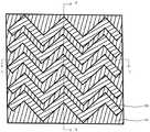
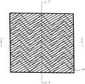
本发明实施例的第一方面提供一种存储器,其包括基底,基底上设置有隔离层,隔离层内间隔排布有多条位线,多条位线沿第一方向排布,且每条位线呈S形。A first aspect of the embodiments of the present invention provides a memory, which includes a substrate, an isolation layer is disposed on the substrate, a plurality of bit lines are arranged at intervals in the isolation layer, the plurality of bit lines are arranged along a first direction, and each The bit lines are S-shaped.
本发明实施例的存储器,基底的隔离层内设置有间隔排布的多条位线,每条位线呈S形且沿第一方向排布,在单位尺寸的基底上,隔离层内设置的每条位线长度增长,后续设置的与位线接触的位线接触柱塞的数量就会增加,后续设置的与位线接触柱塞一一对应的有源区的数量就会增多,后续设置的与有源区一一对应的电容器的数量也会增多,如此,存储器的集成度更高。In the memory of the embodiment of the present invention, a plurality of bit lines arranged at intervals are arranged in the isolation layer of the substrate, and each bit line is S-shaped and arranged along the first direction. As the length of each bit line increases, the number of bit line contact plungers set subsequently that are in contact with the bit line will increase, and the number of subsequently set active regions corresponding to the bit line contact plungers one-to-one will increase. The number of capacitors corresponding to the active regions one-to-one will also increase, so that the integration of the memory is higher.
在一些实施方式中,每条位线包括间隔排布且依次连接的多个第一位线结构和多个第二位线结构,第一位线结构沿第二方向延伸,第二方向相对第一方向倾斜设置,第二位线结构沿第三方向延伸,第三方向相对第一方向倾斜设置,且第三方向与第二方向相对第一方向的倾斜方向相反。In some embodiments, each bit line includes a plurality of first bit line structures and a plurality of second bit line structures arranged at intervals and connected in sequence, the first bit line structures extend along a second direction, and the second direction is opposite to the first bit line structure. One direction is inclined, the second bit line structure extends along a third direction, the third direction is inclined relative to the first direction, and the third direction is opposite to the inclination direction of the second direction relative to the first direction.
在一些实施方式中,每条位线上设置有间隔排布的多个位线接触柱塞,位线接触柱塞设置在隔离层内,且每个位线接触柱塞设置在对应的第一位线结构和第二位线结构的连接位置。In some embodiments, each bit line is provided with a plurality of bit line contact plungers arranged at intervals, the bit line contact plungers are arranged in the isolation layer, and each bit line contact plunger is arranged in a corresponding first The connection position of the bit line structure and the second bit line structure.
在一些实施方式中,每个位线接触柱塞上设置有源区,有源区设置在隔离层内。In some embodiments, an active region is provided on each bit line contact plug, and the active region is provided within the isolation layer.
在一些实施方式中,隔离层内还设置有多条字线,多条字线沿第四方向排布,每条字线沿第一方向延伸,第四方向与第一方向垂直设置。In some embodiments, a plurality of word lines are further provided in the isolation layer, the plurality of word lines are arranged along a fourth direction, each word line extends along a first direction, and the fourth direction is perpendicular to the first direction.
在一些实施方式中,每条字线包括多个栅极和多个字线结构,每个栅极对应设置在一个有源区内,每条字线包括的多个栅极对应设置在同一列有源区内,同一列有源区沿第一方向排布,多个栅极和多个字线结构一一间隔设置,每个字线结构设置在隔离层内,每个字线结构用于连接相邻两个栅极。In some embodiments, each word line includes a plurality of gates and a plurality of word line structures, each of the gates is correspondingly disposed in one active region, and the plurality of gates included in each word line is correspondingly disposed in the same column In the active area, the same column of active areas is arranged along the first direction, a plurality of gates and a plurality of word line structures are arranged one by one at intervals, each word line structure is arranged in the isolation layer, and each word line structure is used for Connect two adjacent gates.
在一些实施方式中,字线包括金属层和介质层,介质层包括第一介质层、第二介质层和第三介质层,第一介质层的顶面设置金属层和第二介质层,第二介质层设置在金属层的相对两侧面,金属层的顶面和第二介质层的顶面设置第三介质层。In some embodiments, the word line includes a metal layer and a dielectric layer, the dielectric layer includes a first dielectric layer, a second dielectric layer and a third dielectric layer, the top surface of the first dielectric layer is provided with a metal layer and a second dielectric layer, and the first dielectric layer is provided with a metal layer and a second dielectric layer. Two dielectric layers are disposed on opposite sides of the metal layer, and a third dielectric layer is disposed on the top surface of the metal layer and the top surface of the second dielectric layer.
在一些实施方式中,每条字线上间隔设置有多个节点接触柱塞,每个节点接触柱塞与有源区的顶端电连接,节点接触柱塞与位线接触柱塞在垂直于基底方向上一一对应。In some embodiments, each word line is provided with a plurality of node contact plugs at intervals, each node contact plug is electrically connected to the top of the active region, and the node contact plug and the bit line contact plug are perpendicular to the substrate. One-to-one correspondence in the direction.
本发明实施例的第二方面提供一种存储器的制备方法,其包括如下步骤:提供基底;在基底上形成多条位线沟槽,多条位线沟槽沿第一方向排布,且每条位线沟槽呈S形;在每条位线沟槽内形成第一隔离层,第一隔离层的厚度小于位线沟槽的深度;在第一隔离层上形成位线,第一隔离层和位线的总厚度小于位线沟槽的深度,多条位线沿第一方向排布,且每条位线呈S形;在位线上形成第二隔离层,第二隔离层的顶面与基底的顶面平齐;去除相邻的隔离墙之间的基底,且保留第一隔离层底面以下的基底,其中,隔离墙包括第一隔离层、位线以及第二隔离层;在相邻的隔离墙之间的间隙内形成第三隔离层,第三隔离层、第二隔离层和第一隔离层共同形成隔离层。A second aspect of the embodiments of the present invention provides a method for fabricating a memory, which includes the following steps: providing a substrate; forming a plurality of bit line trenches on the substrate, the plurality of bit line trenches are arranged along a first direction, and each The bit line trenches are S-shaped; a first isolation layer is formed in each bit line trench, and the thickness of the first isolation layer is less than the depth of the bit line trench; bit lines are formed on the first isolation layer, and the first isolation layer is The total thickness of the layer and the bit line is less than the depth of the bit line trench, a plurality of bit lines are arranged along the first direction, and each bit line is S-shaped; a second isolation layer is formed on the bit line, and the second isolation layer is The top surface is flush with the top surface of the substrate; the substrate between adjacent isolation walls is removed, and the substrate below the bottom surface of the first isolation layer is retained, wherein the isolation wall includes a first isolation layer, a bit line and a second isolation layer; A third isolation layer is formed in the gap between adjacent isolation walls, and the third isolation layer, the second isolation layer and the first isolation layer together form an isolation layer.
本发明实施例的存储器的制备方法,通过在基底上设置呈S形的位线沟槽,进而在S形的位线沟槽内形成呈S形的位线,如此,使得制备的存储器内,在单位尺寸的基底上,隔离层内设置的每条位线长度增长,后续设置的与位线接触的位线接触柱塞的数量就会增加,后续设置的与位线接触柱塞一一对应的有源区的数量就会增多,后续设置的与有源区一一对应的电容器的数量也会增多,存储器的集成度更高。In the preparation method of the memory according to the embodiment of the present invention, an S-shaped bit line trench is arranged on the substrate, and then an S-shaped bit line is formed in the S-shaped bit line trench, so that in the prepared memory, On a substrate with a unit size, the length of each bit line set in the isolation layer increases, and the number of bit line contact plungers that are subsequently set in contact with the bit line will increase, and the subsequently set bit line contact plungers correspond one-to-one. The number of active regions will increase, and the number of capacitors corresponding to the active regions will also increase, and the integration of the memory will be higher.
在一些实施方式中,在第一隔离层上形成位线的步骤中:形成的每条位线包括间隔排布且依次连接的多个第一位线结构和多个第二位线结构,第一位线结构沿第二方向延伸,第二方向相对第一方向倾斜设置,第二位线结构沿第三方向延伸,第三方向相对第一方向倾斜设置,且第三方向与第二方向相对第一方向的倾斜方向相反。In some embodiments, in the step of forming a bit line on the first isolation layer: each formed bit line includes a plurality of first bit line structures and a plurality of second bit line structures that are arranged at intervals and connected in sequence, the first The bit line structure extends along a second direction, the second direction is inclined relative to the first direction, the second bit line structure extends along a third direction, the third direction is inclined relative to the first direction, and the third direction is opposite to the second direction The inclination direction of the first direction is opposite.
在一些实施方式中,在形成第三隔离层之后,还包括:去除第一位线结构和第二位线结构连接位置上的部分隔离层以形成多个凹孔,每个凹孔暴露出位线;在每个凹孔中沉积第一层多晶硅以形成位线接触柱塞。In some embodiments, after the third isolation layer is formed, the method further includes: removing a part of the isolation layer on the connecting position of the first bit line structure and the second bit line structure to form a plurality of concave holes, each concave hole exposing a bit lines; deposit a first layer of polysilicon in each recess to form bit line contact plugs.
在一些实施方式中,在每个凹孔中沉积第一层多晶硅以形成位线接触柱塞的步骤,包括:在每个凹孔中沉积第一层多晶硅,第一层多晶硅填充满凹孔且覆盖在保留下的隔离层上;去除部分第一层多晶硅,保留下的第一层多晶硅位于凹孔中,并且保留下的第一层多晶硅的顶面低于隔离层的顶面,保留在凹孔中的第一层多晶硅形成位线接触柱塞。In some embodiments, the step of depositing a first layer of polysilicon in each recessed hole to form the bit line contact plug includes: depositing a first layer of polysilicon in each recessed hole, the first layer of polysilicon filling the recessed hole and Covering the remaining isolation layer; removing part of the first layer of polysilicon, the remaining first layer of polysilicon is located in the concave hole, and the top surface of the remaining first layer of polysilicon is lower than the top surface of the isolation layer, remaining in the concave hole. The first layer of polysilicon in the hole forms the bit line contact plug.
在一些实施方式中,在每个凹孔中形成位线接触柱塞之后,还包括:在位线接触柱塞上形成第二层多晶硅,第二层多晶硅的顶面与隔离层的顶面平齐;在保留下的隔离层和第二层多晶硅上形成保护层;去除部分保护层、部分第二层多晶硅以及部分隔离层,以形成字线沟槽,字线沟槽沿第四方向排布,且沿第一方向延伸,第四方向与第一方向垂直设置,保留下的第二层多晶硅形成位于字线沟槽两侧的有源区,保留下的保护层内形成与字线沟槽连通的节点柱塞槽,节点柱塞槽的宽度大于字线沟槽的宽度。In some embodiments, after forming the bit line contact plug in each recess, the method further includes: forming a second layer of polysilicon on the bit line contact plug, the top surface of the second layer of polysilicon being flat with the top surface of the isolation layer aligning; forming a protective layer on the remaining isolation layer and the second polysilicon layer; removing part of the protective layer, part of the second polysilicon layer and part of the isolation layer to form word line trenches, and the word line trenches are arranged along the fourth direction , and extends along the first direction, the fourth direction is perpendicular to the first direction, the remaining second layer of polysilicon forms the active region on both sides of the word line trench, and the remaining protective layer is formed with the word line trench For the connected node plug grooves, the width of the node plug grooves is greater than the width of the word line grooves.
在一些实施方式中,保留下的第二层多晶硅经离子注入后形成有源区。In some embodiments, the remaining second layer of polysilicon is ion-implanted to form an active region.
在一些实施方式中,形成字线沟槽后,还包括:在字线沟槽的底部形成第一介质层;在第一介质层上形成第二介质层,第二介质层覆盖有源区侧壁;在字线沟槽内的第一介质层上、且第二介质层远离有源区的侧部形成金属层,金属层填充满字线沟槽和节点柱塞槽,并覆盖在保留下的隔离层和保留下的保护层上;回刻金属层,使金属层低于有源区;在金属层上形成第三介质层,第三介质层的顶面与保护层的底面平齐。In some embodiments, after the word line trench is formed, the method further includes: forming a first dielectric layer at the bottom of the word line trench; forming a second dielectric layer on the first dielectric layer, the second dielectric layer covering the side of the active region wall; a metal layer is formed on the first dielectric layer in the word line trench and on the side of the second dielectric layer away from the active region, the metal layer fills the word line trench and the node plug groove, and covers the reserved On the isolation layer and the remaining protective layer; the metal layer is etched back so that the metal layer is lower than the active area; a third dielectric layer is formed on the metal layer, and the top surface of the third dielectric layer is flush with the bottom surface of the protective layer.
在一些实施方式中,形成第三介质层之后,还包括:在第三介质层上形成第三层多晶硅,第三层多晶硅填充满节点柱塞槽且覆盖保护层;去除部分第三层多晶硅,保留下的第三层多晶硅形成多个节点接触柱塞,每个节点接触柱塞与对应的有源区的顶端电连接,节点接触柱塞与位线接触柱塞在垂直于基底方向上一一对应。In some embodiments, after forming the third dielectric layer, the method further includes: forming a third layer of polysilicon on the third dielectric layer, the third layer of polysilicon filling the node plug grooves and covering the protective layer; removing part of the third layer of polysilicon, The remaining third layer of polysilicon forms a plurality of node contact plugs, each node contact plug is electrically connected to the top of the corresponding active region, and the node contact plug and the bit line contact plug are in a direction perpendicular to the substrate one by one correspond.
除了上面所描述的本发明实施例解决的技术问题、构成技术方案的技术特征以及由这些技术方案的技术特征所带来的有益效果外,本发明实施例提供的存储器及其制备方法所能解决的其他技术问题、技术方案中包含的其他技术特征以及这些技术特征带来的有益效果,将在具体实施方式中作出进一步详细的说明。In addition to the technical problems solved by the embodiments of the present invention described above, the technical features constituting the technical solutions, and the beneficial effects brought about by the technical features of the technical solutions, the memory and the preparation method thereof provided by the embodiments of the present invention can solve the problem. Other technical problems, other technical features included in the technical solution, and the beneficial effects brought about by these technical features will be described in further detail in the specific embodiments.
附图说明Description of drawings
为了更清楚地说明本发明实施例或现有技术中的技术方案,下面将对实施例或现有技术描述中所需要使用的附图作一简单地介绍,显而易见地,下面描述中的附图是本发明的一些实施例,对于本领域普通技术人员来讲,在不付出创造性劳动的前提下,还可以根据这些附图获得其他的附图。In order to more clearly illustrate the embodiments of the present invention or the technical solutions in the prior art, the following briefly introduces the accompanying drawings that need to be used in the description of the embodiments or the prior art. Obviously, the accompanying drawings in the following description These are some embodiments of the present invention. For those of ordinary skill in the art, other drawings can also be obtained according to these drawings without creative efforts.
图1为本发明实施例的存储器的制备方法的流程图;1 is a flowchart of a method for preparing a memory according to an embodiment of the present invention;
图2a为本发明实施例中基底上设置位线沟槽后的结构示意图;2a is a schematic structural diagram of a substrate after bit line trenches are arranged in an embodiment of the present invention;
图2b为图2a中的AA位置的断面图;Fig. 2b is the sectional view of the AA position in Fig. 2a;
图2c为图2a中的BB位置的断面图;Figure 2c is a cross-sectional view of the BB position in Figure 2a;
图3a为本发明实施例中在位线沟槽中设置第一层二氧化硅后的结构示意图;FIG. 3a is a schematic structural diagram of a first layer of silicon dioxide disposed in a bit line trench according to an embodiment of the present invention;
图3b为图3a中的AA位置的断面图;Fig. 3b is the sectional view of the AA position in Fig. 3a;
图3c为图3a中的BB位置的断面图;Fig. 3c is the sectional view of the BB position in Fig. 3a;
图4a为本发明实施例中在位线沟槽中形成第一隔离层后的结构示意图;4a is a schematic structural diagram after forming a first isolation layer in the bit line trench according to an embodiment of the present invention;
图4b为图4a中的AA位置的断面图;Fig. 4b is the sectional view of the AA position in Fig. 4a;
图4c为图4a中的BB位置的断面图;Figure 4c is a cross-sectional view of the BB position in Figure 4a;
图5a为本发明实施例中在位线沟槽中设置金属钨层后的结构示意图;5a is a schematic structural diagram of a tungsten metal layer after a tungsten metal layer is disposed in the bit line trench according to an embodiment of the present invention;
图5b为图5a中的AA位置的断面图;Fig. 5b is the sectional view of the AA position in Fig. 5a;
图5c为图5a中的BB位置的断面图;Figure 5c is a cross-sectional view of the BB position in Figure 5a;
图6a为本发明实施例中在位线沟槽中形成位线后的结构示意图;6a is a schematic structural diagram of a bit line formed in a bit line trench according to an embodiment of the present invention;
图6b为图6a中的AA位置的断面图;Fig. 6b is the sectional view of the AA position in Fig. 6a;
图6c为图6a中的BB位置的断面图;Figure 6c is a cross-sectional view of the BB position in Figure 6a;
图7a为本发明实施例中在位线沟槽中设置第二层二氧化硅后的结构示意图;FIG. 7a is a schematic structural diagram of a second layer of silicon dioxide disposed in the bit line trench according to an embodiment of the present invention;
图7b为图7a中的AA位置的断面图;Figure 7b is a sectional view of the AA position in Figure 7a;
图7c为图7a中的BB位置的断面图;Fig. 7c is a sectional view of the BB position in Fig. 7a;
图8a为本发明实施例中去除部分第二层二氧化硅后的结构示意图;FIG. 8a is a schematic structural diagram after removing part of the second layer of silicon dioxide in an embodiment of the present invention;
图8b为图8a中的AA位置的断面图;Figure 8b is a cross-sectional view of the AA position in Figure 8a;
图8c为图8a中的BB位置的断面图;Figure 8c is a cross-sectional view of the BB position in Figure 8a;
图9a为本发明实施例中去除相邻隔离墙之间的部分基底后的结构示意图;9a is a schematic structural diagram after removing part of the substrate between adjacent partition walls according to an embodiment of the present invention;
图9b为图9a中的AA位置的断面图;Figure 9b is a sectional view of the AA position in Figure 9a;
图9c为图9a中的BB位置的断面图;Figure 9c is a sectional view of the BB position in Figure 9a;
图10a为本发明实施例中在隔离墙之间的间隙设置第三隔离层后的结构示意图;FIG. 10a is a schematic structural diagram after a third isolation layer is arranged in the gap between the isolation walls according to the embodiment of the present invention;
图10b为图10a中的AA位置的断面图;Figure 10b is a sectional view at the AA position in Figure 10a;
图10c为图10a中的BB位置的断面图;Figure 10c is a cross-sectional view at the BB position in Figure 10a;
图11a为本发明实施例中在隔离层上设置凹孔后的结构示意图;FIG. 11a is a schematic structural diagram of the isolation layer provided with concave holes in an embodiment of the present invention;
图11b为图11a中的AA位置的断面图;Fig. 11b is a sectional view at the AA position in Fig. 11a;
图11c为图11a中的BB位置的断面图;Figure 11c is a cross-sectional view at the BB position in Figure 11a;
图12a为本发明实施例中在凹孔中以及保留下的隔离层上设置第一层多晶硅后的结构示意图;12a is a schematic structural diagram of a first layer of polysilicon disposed in the concave hole and on the remaining isolation layer according to an embodiment of the present invention;
图12b为图12a中的AA位置的断面图;Figure 12b is a sectional view at the AA position in Figure 12a;
图12c为图12a中的BB位置的断面图;Figure 12c is a cross-sectional view at the BB position in Figure 12a;
图13a为本发明实施例中去除部分第一层多晶硅后的结构示意图;FIG. 13a is a schematic structural diagram after removing part of the first layer of polysilicon according to an embodiment of the present invention;
图13b为图13a中的AA位置的断面图;Figure 13b is a sectional view at the AA position in Figure 13a;
图13c为图13a中的BB位置的断面图;Figure 13c is a sectional view at the BB position in Figure 13a;
图14a为本发明实施例中在凹孔中形成位线接触柱塞后的结构示意图;14a is a schematic structural diagram of forming a bit line contact plug in a recess in an embodiment of the present invention;
图14b为图14a中的AA位置的断面图;Figure 14b is a sectional view of the AA position in Figure 14a;
图14c为图14a中的BB位置的断面图;Figure 14c is a cross-sectional view at the BB position in Figure 14a;
图14d为本发明实施例中形成位线接触柱塞的流程图;14d is a flowchart of forming a bit line contact plug in an embodiment of the present invention;
图15a为本发明实施例中在凹孔中填充第二层多晶硅并在第二层多晶硅和保留下的隔离层上设置保护层后的结构示意图;15a is a schematic structural diagram of filling a second layer of polysilicon in the concave hole and disposing a protective layer on the second layer of polysilicon and the remaining isolation layer according to an embodiment of the present invention;
图15b为图15a中的AA位置的断面图;Figure 15b is a sectional view of the AA position in Figure 15a;
图15c为图15a中的BB位置的断面图;Figure 15c is a cross-sectional view at the BB position in Figure 15a;
图16a为本发明实施例中形成字线沟槽和节点柱塞槽后并在字线沟槽中形成第一介质层后的结构示意图;16a is a schematic structural diagram of a word line trench and a node plug trench and a first dielectric layer formed in the word line trench according to an embodiment of the present invention;
图16b为图16a中的AA位置的断面图;Figure 16b is a sectional view at the AA position in Figure 16a;
图16c为图16a中的BB位置的断面图;Figure 16c is a sectional view at the BB position in Figure 16a;
图17a为本发明实施例中在字线沟槽中设置第二介质层后的结构示意图;FIG. 17a is a schematic structural diagram after disposing a second dielectric layer in the word line trenches according to an embodiment of the present invention;
图17b为图17a中的AA位置的断面图;Figure 17b is a cross-sectional view at the AA position in Figure 17a;
图17c为图17a中的BB位置的断面图;Figure 17c is a sectional view at the BB position in Figure 17a;
图18a为本发明实施例中在字线沟槽中设置金属层后的结构示意图;18a is a schematic structural diagram of a metal layer after a word line trench is disposed in an embodiment of the present invention;
图18b为图18a中的AA位置的断面图;Figure 18b is a cross-sectional view at the AA position in Figure 18a;
图18c为图18a中的BB位置的断面图;Figure 18c is a cross-sectional view at the BB position in Figure 18a;
图19a为本发明实施例中去除保护层顶面以上的金属层后的结构示意图;FIG. 19a is a schematic structural diagram after removing the metal layer above the top surface of the protective layer in an embodiment of the present invention;
图19b为图19a中的AA位置的断面图;Figure 19b is a sectional view at the AA position in Figure 19a;
图19c为图19a中的BB位置的断面图;Figure 19c is a cross-sectional view at the BB position in Figure 19a;
图20a为本发明实施例中去除字线沟槽中的部分金属层并在金属层上设置第三介质层后的结构示意图;FIG. 20a is a schematic structural diagram after removing part of the metal layer in the word line trench and disposing a third dielectric layer on the metal layer according to an embodiment of the present invention;
图20b为图20a中的AA位置的断面图;Figure 20b is a sectional view at the AA position in Figure 20a;
图20c为图20a中的BB位置的断面图;Figure 20c is a cross-sectional view at the BB position in Figure 20a;
图21a为本发明实施例中在节点柱塞槽中设置第三层多晶硅后的结构示意图;21a is a schematic structural diagram of a third layer of polysilicon disposed in a node plug groove according to an embodiment of the present invention;
图21b为图21a中的AA位置的断面图;Figure 21b is a sectional view at the AA position in Figure 21a;
图21c为图21a中的BB位置的断面图。Figure 21c is a cross-sectional view at the BB position in Figure 21a.
附图标记:Reference number:
100:基底; 101:位线沟槽;100: substrate; 101: bit line trench;
200:第一隔离层; 201:第一层二氧化硅;200: the first isolation layer; 201: the first layer of silicon dioxide;
300:位线; 301:金属钨层;300: bit line; 301: metal tungsten layer;
302:第一位线结构; 303:第二位线结构;302: first bit line structure; 303: second bit line structure;
400:第二隔离层; 401:第二层二氧化硅;400: the second isolation layer; 401: the second layer of silicon dioxide;
500:隔离墙; 600:第三隔离层;500: separation wall; 600: third separation layer;
700:隔离层; 701:凹孔;700: isolation layer; 701: concave hole;
800:位线接触柱塞; 801:第一层多晶硅;800: bit line contact plunger; 801: first layer polysilicon;
900:第二层多晶硅; 901:字线沟槽;900: second layer of polysilicon; 901: word line trench;
902:有源区; A00:保护层;902: active area; A00: protective layer;
A01:节点柱塞槽; B00:第一介质层;A01: Node plunger groove; B00: First dielectric layer;
C00:第二介质层; D00:金属层;C00: second dielectric layer; D00: metal layer;
E00:第三介质层; F00:第三层多晶硅。E00: the third dielectric layer; F00: the third layer of polysilicon.
具体实施方式Detailed ways
在相关技术中,动态随机存储器一般是先形成浅沟槽隔离结构定义出有源区,然后在有源区中刻蚀形成埋入式字线,在埋入式字线之间形成位线接触柱塞,再通过位线连接各位线接触柱塞;且现有技术中较主流的动态随机存储器是3HPAA乘2HPWL结构,3HPAA乘2HPWL确定一个位单元面积,3HPAA乘2HPWL指3倍的有源区的半节距乘以2倍的字线的半节距。然而,这种结构的动态随机存储器,单位尺寸的基底上,每条位线的长度短,每条位线对应设置的位线接触柱塞数量少,后续对应设置的有源区的数量较少,后续对应设置的电容器的数量较少,存储器的集成度低。In the related art, in the DRAM, a shallow trench isolation structure is generally formed to define an active region, and then buried word lines are formed in the active region by etching, and bit line contacts are formed between the buried word lines. The plunger is connected to the plunger through the bit line; and the mainstream dynamic random access memory in the prior art is a 3HPAA multiplied by 2HPWL structure, 3HPAA multiplied by 2HPWL to determine a bit cell area, 3HPAA multiplied by 2HPWL refers to 3 times the active area The half pitch is multiplied by 2 times the half pitch of the word line. However, in the dynamic random access memory of this structure, on the substrate of unit size, the length of each bit line is short, the number of bit line contact plungers corresponding to each bit line is small, and the number of active regions corresponding to the subsequent settings is small. , the number of capacitors set subsequently is relatively small, and the integration degree of the memory is low.
为此,本发明实施例提供一种存储器及其制备方法,通过在基底上形成呈S形的位线,使得单位尺寸的基底上,每条位线的长度增长,后续设置的与位线接触的位线接触柱塞的数量就会增多,后续设置的与位线接触柱塞一一对应的有源区的数量就会增多,后续设置的与有源区一一对应的电容器的数量也会增多,如此,提高存储器的集成度。To this end, embodiments of the present invention provide a memory and a method for fabricating the same. By forming S-shaped bit lines on a substrate, the length of each bit line increases on a substrate with a unit size, and the subsequently arranged bit lines are in contact with the bit lines. The number of bit line contact plungers will increase, the number of subsequently set active regions corresponding to the bit line contact plungers will increase, and the number of subsequently set capacitors corresponding to the active regions will also increase. Increase, thus, improve the integration degree of memory.
为了使本发明实施例的上述目的、特征和优点能够更加明显易懂,下面将结合本发明实施例中的附图,对本发明实施例中的技术方案进行清楚、完整地描述。显然,所描述的实施例仅仅是本发明的一部分实施例,而不是全部的实施例。基于本发明中的实施例,本领域普通技术人员在没有作出创造性劳动的前提下所获得的所有其它实施例,均属于本发明保护的范围。In order to make the above objects, features and advantages of the embodiments of the present invention more clearly and easily understood, the technical solutions in the embodiments of the present invention will be clearly and completely described below with reference to the accompanying drawings in the embodiments of the present invention. Obviously, the described embodiments are only some, but not all, embodiments of the present invention. Based on the embodiments of the present invention, all other embodiments obtained by those of ordinary skill in the art without creative work fall within the protection scope of the present invention.
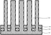
如图1所示,本发明实施例提供一种存储器的制备方法,其包括如下步骤:As shown in FIG. 1 , an embodiment of the present invention provides a method for preparing a memory, which includes the following steps:
S01:提供基底,基底的材料可以是硅、锗等本领域技术人员熟知的半导体基底材料。S01: Provide a substrate, and the material of the substrate can be a semiconductor substrate material well known to those skilled in the art, such as silicon and germanium.
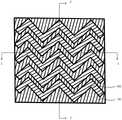
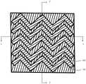
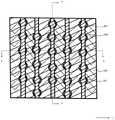
S02:在基底上形成多条位线沟槽,多条位线沟槽间隔设置,多条位线沟槽沿第一方向排布,且每条位线沟槽呈S形,其中,第一方向如图2a示出的X方向,该步骤形成的结构如图2a、图2b以及图2c所示,该步骤形成的结构中,多条位线沟槽101间隔排布,并且沿第一方向排布,每条位线沟槽101呈S形。S02: forming a plurality of bit line trenches on the substrate, the plurality of bit line trenches are arranged at intervals, the plurality of bit line trenches are arranged along the first direction, and each bit line trench is S-shaped, wherein the first The direction is the X direction as shown in FIG. 2a, and the structure formed in this step is shown in FIG. 2a, FIG. 2b and FIG. 2c. In the structure formed in this step, a plurality of
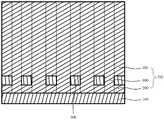
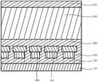
S03:在每条位线沟槽101内形成第一隔离层,第一隔离层的厚度小于位线沟槽101的深度,第一隔离层的材料例如可以为二氧化硅,第一隔离层可以通过沉积的方法形成在位线沟槽101内,第一隔离层形成过程中,首先,在设置有位线沟槽101的基底100上形成第一层二氧化硅,第一层二氧化硅填充满位线沟槽101,且覆盖在保留下的基底100上,去除高于基底100顶面的部分第一层二氧化硅,该步骤形成的结构如图3a、图3b以及图3c所示,该步骤形成的结构中,第一层二氧化硅201位于位线沟槽101内,且第一层二氧化硅201与基底100的顶面平齐;其次,继续去除部分第一层二氧化硅201,仅保留位线沟槽101内的部分第一层二氧化硅201,且保留在位线沟槽101内的第一层二氧化硅201的厚度小于位线沟槽101的深度,以形成第一隔离层,该步骤形成的结构如图4a、图4b以及图4c所示,该步骤形成的结构中,第一隔离层200位于位线沟槽101内,且第一隔离层200的厚度小于位线沟槽101的深度,第一隔离层200的顶面低于位线沟槽101的槽口。S03: A first isolation layer is formed in each
S04:在第一隔离层200上形成位线,第一隔离层200和位线的总厚度小于位线沟槽101的槽深,多条位线沿第一方向排布,且每条位线呈S形,位线的材料例如可以是金属钨,位线可以采用沉积的方法形成在位线沟槽101内的第一隔离层200上。位线形成过程中,首先,在设置有位线沟槽101以及第一隔离层200的基底100上形成一层金属钨层,金属钨层填充满位线沟槽101,且覆盖在保留下的基底100上,该步骤形成的结构如图5a、图5b以及图5c所示,图5a虚线用于显示位线沟槽101的位置,该步骤形成的结构中,金属钨层301位于位线沟槽101内,且该层金属钨层301还覆盖在保留下的基底100的顶面;其次,去除部分金属钨层301,仅保留位线沟槽101内的金属钨层301,且保留在位线沟槽101内的金属钨层301的厚度小于位线沟槽101的深度,以形成位线,该步骤形成的结构如图6a、图6b以及图6c所示,该步骤形成的结构中,位线300位于位线沟槽101内的第一隔离层200上,位线300的顶面低于位线沟槽101的槽口,位线300的厚度加第一隔离层200的厚度小于位线沟槽101的槽深。S04: forming a bit line on the
请参阅图6a,在第一隔离层200上形成位线300的步骤中:形成的每条位线300包括间隔排布且依次连接的多个第一位线结构302和多个第二位线结构303,第一位线结构302沿第二方向延伸,第二方向相对第一方向倾斜设置,第二位线结构303沿第三方向延伸,第三方向相对第一方向倾斜设置,且第三方向与第二方向相对第一方向的倾斜方向相反,其中,第二方向如图6a示出的Y方向,第三方向如图6a示出的Z方向。Referring to FIG. 6a, in the step of forming the bit lines 300 on the first isolation layer 200: each
S05:在位线300上形成第二隔离层,第二隔离层的顶面与基底100的顶面平齐,第二隔离层的材料和第一隔离层200的材料可为同一种材料,第二隔离层的材料例如为二氧化硅,第二隔离层可以采用沉积的方法形成在位线沟槽101内的位线300上。第二隔离层形成过程中,首先,在设置有位线300的基底100上形成第二层二氧化硅,第二层二氧化硅填充满位线沟槽101,且覆盖在保留下的基底100上,该步骤形成的结构如图7a、图7b以及图7c所示,图7a虚线用于显示位线沟槽101的位置,该步骤形成的结构中,第二层二氧化硅401位于位线沟槽101内,且第二层二氧化硅401还覆盖在保留下的基底100的顶面;其次,去除部分第二层二氧化硅401,仅保留位线沟槽101内的第二层二氧化硅401,且保留在位线沟槽101内的第二层二氧化硅401的顶面与基底100的顶面平齐,以形成第二隔离层,该步骤形成的结构如图8a、图8b以及图8c所示,该步骤形成的结构中,第二隔离层400位于位线沟槽101内的位线300上,第二隔离层400的厚度加上位线300的厚度,再加上第一隔离层200的厚度等于位线沟槽101的槽深。S05: A second isolation layer is formed on the
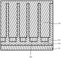
S06:去除相邻的隔离墙之间的基底100,且保留第一隔离层200底面以下的基底100,其中,隔离墙包括第一隔离层200、位线300以及第二隔离层400,去除相邻的隔离墙之间的基底100可以采用刻蚀的方法,该步骤形成的结构如图9a、图9b以及图9c所示,该步骤形成的结构中,基底100的顶面设置有多个间隔排布的隔离墙500,每个隔离墙500包括设置在基底100上的第一隔离层200、设置在第一隔离层200上的位线300,以及设置在位线300上的第二隔离层400,其中,每个隔离墙500呈S形,多个隔离墙500沿第一方向排布。S06: Remove the
S07:在相邻的隔离墙500之间的间隙内形成第三隔离层,第三隔离层、第二隔离层400和第一隔离层200共同形成隔离层,第三隔离层的材料与第一隔离层200的材料、第二隔离层400的材料可为同一种材料,第三隔离层的材料例如为二氧化硅,第三隔离层可以采用沉积的方法形成在相邻两个隔离墙500之间的间隙内。该步骤形成的结构如图10a、图10b以及图10c所示,该步骤形成的结构中,基底100上间隔设置有隔离墙500和第三隔离层600,隔离墙500包括设置在基底100上的第一隔离层200、设置在第一隔离层200上的位线300,以及设置在位线300上的第二隔离层400;位线300正下方为第一隔离层200,位线300的正上方为第二隔离层400,位线300的两侧为第三隔离层600,位线300形成在第一隔离层200、第二隔离层400以及第三隔离层600形成的隔离层700内,隔离层700能够实现相邻位线300之间的绝缘,图10a中虚线用于显示位线沟槽101的位置,图10b和图10c中虚线用于显示第一隔离层200、第二隔离层400与第三隔离层600在不同的工艺步骤中形成。S07: A third isolation layer is formed in the gap between
本发明实施例的存储器的制备方法,通过在基底100上设置呈S形的位线沟槽101,进而在S形的位线沟槽101内形成呈S形的位线300,如此,使得制备的存储器内,在单位尺寸的基底100上,隔离层700内设置的位线300长度增长,后续设置的与位线300接触的位线接触柱塞的数量就会增加,后续设置的与位线接触柱塞一一对应的有源区的数量就会增多,后续设置的与有源区一一对应的电容器的数量也会增多,存储器的集成度更高。In the preparation method of the memory according to the embodiment of the present invention, an S-shaped
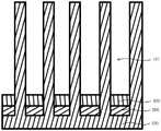
本发明实施例的存储器的制备方法制备的存储器是2HPAA乘2HPWL结构,2HPAA乘2HPWL确定一个位单元面积,2HPAA乘2HPWL指2倍的有源区的半节距乘以2倍的字线的半节距,2HPAA乘2HPWL结构形成的4F2存储单元的面积会缩小至3HPAA乘2HPWL结构形成的6F2存储单元的三分之二左右,相当于4F2存储结构的存储密度更大,集成度更高。The memory prepared by the memory preparation method of the embodiment of the present invention has a structure of 2HPAA by 2HPWL, 2HPAA by 2HPWL determines the area of a bit cell, and 2HPAA by 2HPWL refers to twice the half pitch of the active area and twice the half of the word line. The area of the 4F2 memory cell formed by the 2HPAA multiplied by 2HPWL structure will be reduced to about two-thirds of the 6F2 memory cell formed by the 3HPAA multiplied by 2HPWL structure, which is equivalent to the higher storage density and higher integration of the 4F2 memory structure.
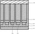
请继续参照图1,在形成第三隔离层600之后,还包括:Please continue to refer to FIG. 1 , after the
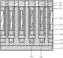
S08:去除第一位线结构302和第二位线结构303连接位置上的部分隔离层700以形成多个凹孔,每个凹孔暴露出位线300,凹孔的形状可以为圆孔,去除第一位线结构302和第二位线结构303连接位置上的部分隔离层700可以采用刻蚀的方式形成凹孔,该步骤形成的结构如图11a、图11b以及图11c所示,该步骤形成的结构中,每个凹孔701位于第一位线结构302和第二位线结构303的连接位置,每个凹孔701暴露出与其对应的位线300,其中,图11a中虚线用于显示位线沟槽101的位置,图11b和图11c中虚线用于显示第一隔离层200与第三隔离层600在不同的工艺步骤中形成。S08: Remove part of the
S09:在每个凹孔701中沉积第一层多晶硅以形成位线接触柱塞,在每个凹孔701中沉积第一层多晶硅可以采用化学气相沉积法(英文名称为Chemical Vapor Deposition,英文简称为CVD),也可以采用原子层沉积法(英文名称为Atomic Layer Deposition,英文简称为ALD),且在沉积第一层多晶硅的同时,掺杂改变第一层多晶硅电学特性的离子,例如掺杂磷离子或者硼离子。该步骤形成的结构如图14a、图14b以及图14c所示,该步骤形成的结构中,位线接触柱塞800位于凹孔701内,位线接触柱塞800的顶面低于第三隔离层600的顶面以及第二隔离层400的顶面,位线接触柱塞800的厚度例如可以为50纳米(nm),其中,图14a中虚线用于显示位线沟槽101的位置,图14b和图14c中虚线用于显示第一隔离层200与第三隔离层600在不同的工艺步骤中形成。S09: depositing a first layer of polysilicon in each
请参阅图14d,在每个凹孔701中沉积第一层多晶硅以形成位线接触柱塞800的步骤,包括:Referring to FIG. 14d, the step of depositing a first layer of polysilicon in each
S91:在每个凹孔701中沉积第一层多晶硅,第一层多晶硅填充满凹孔701且覆盖在保留下的隔离层700上,该步骤形成的结构如图12a、图12b以及图12c所示,该步骤形成的结构中,第一层多晶硅801填充满凹孔701,且第一层多晶硅801覆盖在保留下的隔离层700上,其中,图12a中虚线用于显示位线沟槽101的位置以及凹孔701的位置,图12b和图12c中虚线用于显示第一隔离层200与第三隔离层600在不同的工艺步骤中形成。S91 : depositing a first layer of polysilicon in each
S92:去除部分第一层多晶硅801,保留下的第一层多晶硅801位于凹孔701中,并且保留下的第一层多晶硅801的顶面低于隔离层700的顶面,保留在凹孔701中的第一层多晶硅801形成位线接触柱塞800,该步骤形成的结构如图14a、图14b以及图14c所示,该步骤形成的结构中,第一层多晶硅801填充在凹孔701内,第一层多晶硅801的顶面低于第三隔离层600的顶面以及第二隔离层400的顶面,保留在凹孔701中的第一层多晶硅801形成位线接触柱塞800。其中,当去除第三隔离层600以及第二隔离层400顶面的第一层多晶硅801,形成的结构如图13a、图13b以及图13c所示,该结构中,第一层多晶硅801填充在凹孔701内,第一层多晶硅801的顶面与第三隔离层600的顶面以及第二隔离层400的顶面平齐,图13a中虚线用于显示位线沟槽101的位置,图13b和图13c中虚线用于显示第一隔离层200与第三隔离层600在不同的工艺步骤中形成,继续去除凹孔701中的部分第一层多晶硅801,形成的结构如图14a、图14b以及图14c所示。S92 : remove part of the first layer of
请继续参照图1,在每个凹孔701中形成位线接触柱塞800之后,还包括:Please continue to refer to FIG. 1 , after the bit
S0A:在位线接触柱塞800上形成第二层多晶硅,第二层多晶硅的顶面与隔离层700的顶面平齐,第二层多晶硅可以采用沉积的方法形成在位线接触柱塞800上,该步骤形成的结构请参阅图15a、图15b以及图15c所示,该步骤形成的结构中,第二层多晶硅900的底面与位线接触柱塞800接触,第二层多晶硅900的顶面与隔离层700的顶面平齐,其中,图15a中虚线用于显示位线沟槽101的位置以及凹孔701的位置,图15b和图15c中虚线用于显示第一隔离层200与第三隔离层600在不同的工艺步骤中形成。SOA: A second layer of polysilicon is formed on the bit
S0B:在保留下的隔离层700和第二层多晶硅900上形成保护层,保护层的材料例如可以是氮化硅,保护层也可以采用沉积的方式形成在保留下的隔离层700和第二层多晶硅900上,该步骤形成的结构如图15a、图15b以及图15c所示,该步骤形成的结构中,保护层A00设置在第二层多晶硅900和保留下的隔离层700上,该步骤中,保留下的隔离层700包括第三隔离层600、第一隔离层200以及部分第二隔离层400。S0B: A protective layer is formed on the remaining
S0C:去除部分保护层A00、部分第二层多晶硅900以及部分隔离层700,以形成字线沟槽,字线沟槽沿第四方向排布,且沿第一方向延伸,第四方向与第一方向垂直设置,第四方向如图16a所示的U方向,保留下的第二层多晶硅900形成位于字线沟槽两侧的有源区,保留下的保护层A00内形成与字线沟槽连通的节点柱塞槽,节点柱塞槽的宽度大于字线沟槽的宽度。该步骤形成的结构中,字线沟槽901沿第一方向延伸,多个字线沟槽901沿第四方向排布,字线沟槽901的宽度小于第二层多晶硅900的宽度,保留下的第二层多晶硅900位于每个字线沟槽901的两侧,保留下的第二层多晶硅900构成有源区902,字线沟槽901的宽度小于节点柱塞槽A01的宽度,节点柱塞槽A01暴露出有源区902的顶面。SOC: remove part of the protective layer A00, part of the second layer of
在步骤S0C中,保留下的第二层多晶硅900,需经离子注入后形成有源区902,离子注入的离子可以是硼离子或磷离子,在第二层多晶硅900上注入离子,可以使得形成的有源区902设置有源/漏极。In step SOC, the remaining second layer of
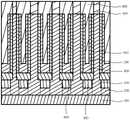
请继续参照图1,形成字线沟槽901后,还包括:Please continue to refer to FIG. 1 , after the
S0D:在字线沟槽901的底部形成第一介质层,第一介质层的材料可以为二氧化硅,第一介质层也可以采用沉积的方法形成在字线沟槽901的底部。该步骤形成的结构如图16a、图16b以及图16c所示,该步骤形成的结构中,第一介质层B00设置在字线沟槽901内,且第一介质层B00的厚度小于字线沟槽901的深度,第一介质层B00的顶面低于字线沟槽901的槽口,其中,图16a中虚线用于显示位线沟槽101的位置,图16b和图16c中虚线用于显示第一隔离层200、第三隔离层600以及第一介质层B00在不同的工艺步骤中形成。SOD: A first dielectric layer is formed at the bottom of the
S0E:在第一介质层B00上形成第二介质层,第二介质层覆盖有源区902侧壁,第二介质层的材料例如可以是二氧化硅,第二介质层可以通过原位水汽法(英文名称为in-situsteam generation,英文简称为ISSG)制备,第二介质层的厚度大约可以为5nm,该步骤形成的结构如图17a、图17b以及图17c所示,该步骤形成的结构中,第二介质层C00设置在第一介质层B00上,且第二介质层C00覆盖在有源区902的侧壁,第二介质层C00的厚度小于字线沟槽901槽宽的一半,其中,图17a中虚线用于显示位线沟槽101的位置,图16b和图16c中虚线用于显示第一隔离层200、第三隔离层600、第一介质层B00和第二介质层C00在不同的工艺步骤中形成。SOE: A second dielectric layer is formed on the first dielectric layer B00. The second dielectric layer covers the sidewall of the
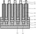
S0F:在字线沟槽901内的第一介质层B00上、且第二介质层C00远离有源区902的侧部形成金属层,金属层填充满字线沟槽901和节点柱塞槽A01,并覆盖在保留下的隔离层700和保留下的保护层A00上;金属层的材料例如可以是金属钨,金属层例如可以采用沉积的方法设置在字线沟槽901内的第一介质层B00和第二介质层C00形成的空间内。该步骤形成的结构如图18a、图18b以及图18c所示,该步骤形成的结构中,金属层D00填充满字线沟槽901和节点柱塞槽A01,且金属层D00覆盖在保留下的隔离层700和保留下的保护层A00上,其中,图18a中虚线用于显示位线沟槽101的位置以及凹孔701的位置,图18b和图18c中虚线用于显示第一隔离层200、第三隔离层600、第一介质层B00和第二介质层C00在不同的工艺步骤中形成。S0F: A metal layer is formed on the first dielectric layer B00 in the
S0G:回刻金属层D00,使金属层D00的顶面低于有源区902的顶面,回刻金属层D00可以采用刻蚀的方式进行,该步骤形成的结构请参阅图20a、图20b以及图20c所示,该步骤形成的结构中,金属层D00设置在字线沟槽901内的第一介质层B00和第二介质层C00围合出的槽内,金属层D00的顶面低于有源区902的顶面。其中,回刻金属层D00时,当回刻的金属层D00的顶面与保护层A00的顶面平齐时,形成的结构如图19a、图19b以及图19c所示,该结构中,金属层D00填充满字线沟槽901和节点柱塞槽A01,且金属层D00的顶面与保护层A00的顶面平齐,其中,图19a中虚线用于显示位线沟槽101的位置,图19b和图19c中虚线用于显示第一隔离层200、第三隔离层600、第一介质层B00和第二介质层C00在不同的工艺步骤中形成。S0G: The metal layer D00 is etched back so that the top surface of the metal layer D00 is lower than the top surface of the
S0H:在金属层D00上形成第三介质层,第三介质层的顶面与保护层A00的底面平齐,第三介质层的材料例如可以是二氧化硅,第三介质层例如可以采用沉积的方法形成在金属层D00上,该步骤形成的结构如图20a、图20b以及图20c所示,该步骤形成的结构中,第三介质层E00的底面与金属层D00的顶面接触,第三介质层E00的顶面与有源区902平齐,金属层D00形成字线,其中,图20a中虚线用于显示位线沟槽101的位置,图20b和图20c中虚线用于显示第一隔离层200、第三隔离层600、第一介质层B00、第二介质层C00和第三介质层E00在不同的工艺步骤中形成。S0H: A third dielectric layer is formed on the metal layer D00, the top surface of the third dielectric layer is flush with the bottom surface of the protective layer A00, the material of the third dielectric layer can be silicon dioxide, for example, the third dielectric layer can be deposited 20a, 20b and 20c. In the structure formed in this step, the bottom surface of the third dielectric layer E00 is in contact with the top surface of the metal layer D00, and the first The top surface of the three dielectric layers E00 is flush with the
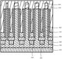
请继续参照图1,形成第三介质层E00之后,还包括:Please continue to refer to FIG. 1 , after the third dielectric layer E00 is formed, it further includes:
S0I:在第三介质层E00上形成第三层多晶硅,第三层多晶硅填充满节点柱塞槽A01且覆盖保护层A00,第三层多晶硅可以采用化学气相沉积方法(英文名称为Chemical VaporDeposition,英文简称为CVD)填充满节点柱塞槽A01,并覆盖在保护层A00上,且在沉积第三层多晶硅的同时,掺杂改变第三层多晶硅电学特性的离子,例如掺杂磷离子或者硼离子。该步骤形成的结构中,第三层多晶硅F00的底面与第三介质层E00的顶面和有源区902的顶面接触,第三层多晶硅F00填充满节点柱塞槽A01,第三层多晶硅F00顶面覆盖在保护层A00的顶面上。SOI: A third layer of polysilicon is formed on the third dielectric layer E00. The third layer of polysilicon fills the node plug groove A01 and covers the protective layer A00. CVD for short) fills the node plug groove A01 and covers the protective layer A00, and at the same time of depositing the third layer of polysilicon, doping with ions that change the electrical properties of the third layer of polysilicon, such as doping phosphorus ions or boron ions . In the structure formed in this step, the bottom surface of the third layer of polysilicon F00 is in contact with the top surface of the third dielectric layer E00 and the top surface of the
S0J:去除部分第三层多晶硅F00,保留下的第三层多晶硅F00形成多个节点接触柱塞,每个节点接触柱塞与对应的有源区902的顶端电连接,节点接触柱塞与位线接触柱塞800在垂直于基底100方向上一一对应。去除部分第三层多晶硅F00时,首先,去除保护层A00的顶面以上的第三层多晶硅F00,此步骤形成的结构如图21a、图21b以及图21c所示,该步骤形成的结构中,第三层多晶硅F00的底面与第三介质层E00的顶面和有源区902的顶面接触,第三层多晶硅F00填充满节点柱塞槽A01,第三层多晶硅F00顶面与保护层A00的顶面平齐,其中,图21a中虚线用于显示位线沟槽101的位置,图21b和图21c中虚线用于显示第一隔离层200、第三隔离层600、第一介质层B00、第二介质层C00和第三介质层E00在不同的工艺步骤中形成。其次,去除节点柱塞槽A01中的部分第三层多晶硅F00,该步骤形成的结构中,每个节点柱塞槽A01中形成多个节点接触柱塞,且每个节点接触柱塞与对应的有源区902的顶端电连接,节点接触柱塞与位线接触柱塞800在垂直于基底100方向上一一对应。S0J: Part of the third layer of polysilicon F00 is removed, and the remaining third layer of polysilicon F00 forms a plurality of node contact plugs, each node contact plug is electrically connected to the top of the corresponding
本发明实施例提供的存储器,其包括基底100,基底100上设置有隔离层700,隔离层700内间隔排布有多条位线300,多条位线300沿第一方向排布,且每条位线300呈S形,第一方向如图2a示出的X方向。The memory provided by the embodiment of the present invention includes a
本发明实施例的存储器,基底100的隔离层700内设置有间隔排布的多条位线300,每条位线300呈S形且沿第一方向排布,在单位尺寸的基底100上,隔离层700内设置的位线300长度增长,后续设置的与位线300接触的位线接触柱塞800的数量就会增加,后续设置的与位线接触柱塞800一一对应的有源区902的数量就会增多,后续设置的与有源区902一一对应的电容器的数量也会增多,如此,存储器的集成度更高。In the memory according to the embodiment of the present invention, the
请参阅图6a,每条位线300包括间隔排布且依次连接的多个第一位线结构302和多个第二位线结构303,第一位线结构302沿第二方向延伸,第二方向相对第一方向倾斜设置,第二位线结构303沿第三方向延伸,第三方向相对第一方向倾斜设置,且第三方向与第二方向相对第一方向的倾斜方向相反。在如图6a示出的实施方式中,每条位线300包括三个第一位线结构302和三个第二位线结构303,三个第一位线结构302和三个第二位线结构303间隔排布且依次连接,第一位线结构302沿第二方向延伸,第二方向如图6a示出的Y方向,第二位线结构303沿第三方向延伸,第三方向如图6a示出的Z方向,Y方向和Z方向相对图2a示出的X方向的倾斜方向相反。Referring to FIG. 6a, each
请参阅图6a、图8b、图14a、图14b以及图14c,每条位线300上设置有间隔排布的多个位线接触柱塞800,位线接触柱塞800设置在隔离层700内,且每个位线接触柱塞800设置在对应的第一位线结构302和第二位线结构303的连接位置。在如图6a和14a示出的实施方式中,每条位线300上方设置有五个位线接触柱塞800,每个位线接触柱塞800设置在相连的第一位线结构302和第二位线结构303的连接处。6a, 8b, 14a, 14b and 14c, each
请参阅图8b、图16a、图16b以及图16c,每个位线接触柱塞800上设置有源区902,有源区902设置在隔离层700内。在如图8b和16b示出的实施方式中,有源区902设置在隔离层700内,有源区902与位线300通过位线接触柱塞800连接,有源区902的底面与位线接触柱塞800的顶面接触,位线接触柱塞800的底面与位线300的顶面接触。Referring to FIGS. 8b , 16a , 16b and 16c , each bit
隔离层700内还设置有多条字线,多条字线沿第四方向排布,每条字线沿第一方向延伸,第四方向与第一方向垂直设置,第四方向如图16a示出的U方向。The
每条字线包括多个栅极和多个字线结构,每个栅极对应设置在一个有源区902内,每条字线包括的多个栅极对应设置在同一列有源区902内,同一列有源区902沿第一方向排布,多个栅极和多个字线结构一一间隔设置,每个字线结构设置在隔离层700内,每个字线结构用于连接相邻两个栅极。在如图20a、图20b以及图20c示出的实施方式中,每条字线包括五个栅极和五个字线结构,栅极至少由设置在有源区902内的金属层D00构成,字线结构至少由设置在隔离层700内的金属层D00构成,五个栅极和五个字线结构间隔设置。Each word line includes a plurality of gates and a plurality of word line structures, each gate is correspondingly disposed in one
请参阅图20a、图20b以及图20c,字线包括金属层D00和介质层,介质层包括第一介质层B00、第二介质层C00和第三介质层E00,第一介质层B00设置在位线接触柱塞800和隔离层700上,第一介质层B00的顶面设置金属层D00和第二介质层C00,金属层D00的顶面和第二介质层C00的顶面平齐,第二介质层C00设置在金属层D00的相对两侧面,金属层D00的顶面和第二介质层C00的顶面设置第三介质层E00。20a, 20b and 20c, the word line includes a metal layer D00 and a dielectric layer, the dielectric layer includes a first dielectric layer B00, a second dielectric layer C00 and a third dielectric layer E00, the first dielectric layer B00 is set in place On the
每条字线上间隔设置有多个节点接触柱塞,每个节点接触柱塞与有源区902的顶端电连接,节点接触柱塞与位线接触柱塞800在垂直于基底100方向上一一对应。A plurality of node contact plugs are arranged at intervals on each word line, each node contact plug is electrically connected to the top of the
本说明书中各实施例或实施方式采用递进的方式描述,每个实施例重点说明的都是与其他实施例的不同之处,各个实施例之间相同相似部分相互参见即可。The embodiments or implementations in this specification are described in a progressive manner, and each embodiment focuses on the differences from other embodiments, and the same and similar parts between the various embodiments may be referred to each other.
在本说明书的描述中,参考术语“一个实施方式”、“一些实施方式”、“示意性实施方式”、“示例”、“具体示例”、或“一些示例”等的描述意指结合实施方式或示例描述的具体特征、结构、材料或者特点包含于本发明的至少一个实施方式或示例中。在本说明书中,对上述术语的示意性表述不一定指的是相同的实施方式或示例。而且,描述的具体特征、结构、材料或者特点可以在任何的一个或多个实施方式或示例中以合适的方式结合。In the description of this specification, reference to the terms "one embodiment," "some embodiments," "exemplary embodiment," "example," "specific example," or "some examples," or the like, is meant to incorporate embodiments. A particular feature, structure, material, or characteristic described or exemplified is included in at least one embodiment or example of the present invention. In this specification, schematic representations of the above terms do not necessarily refer to the same embodiment or example. Furthermore, the particular features, structures, materials or characteristics described may be combined in any suitable manner in any one or more embodiments or examples.
最后应说明的是:以上各实施例仅用以说明本发明的技术方案,而非对其限制;尽管参照前述各实施例对本发明进行了详细的说明,本领域的普通技术人员应当理解:其依然可以对前述各实施例所记载的技术方案进行修改,或者对其中部分或者全部技术特征进行等同替换;而这些修改或者替换,并不使相应技术方案的本质脱离本发明各实施例技术方案的范围。Finally, it should be noted that the above embodiments are only used to illustrate the technical solutions of the present invention, but not to limit them; although the present invention has been described in detail with reference to the foregoing embodiments, those of ordinary skill in the art should understand that: The technical solutions described in the foregoing embodiments can still be modified, or some or all of the technical features thereof can be equivalently replaced; and these modifications or replacements do not make the essence of the corresponding technical solutions deviate from the technical solutions of the embodiments of the present invention. scope.
Claims (13)
Translated fromChinesePriority Applications (3)
| Application Number | Priority Date | Filing Date | Title |
|---|---|---|---|
| CN202110240857.0ACN113053896B (en) | 2021-03-04 | 2021-03-04 | Memory and method of making the same |
| PCT/CN2021/101283WO2022183629A1 (en) | 2021-03-04 | 2021-06-21 | Memory and manufacturing method therefor |
| US17/460,988US11877441B2 (en) | 2021-03-04 | 2021-08-30 | Memory and fabricating method thereof |
Applications Claiming Priority (1)
| Application Number | Priority Date | Filing Date | Title |
|---|---|---|---|
| CN202110240857.0ACN113053896B (en) | 2021-03-04 | 2021-03-04 | Memory and method of making the same |
Publications (2)
| Publication Number | Publication Date |
|---|---|
| CN113053896A CN113053896A (en) | 2021-06-29 |
| CN113053896Btrue CN113053896B (en) | 2022-07-08 |
Family
ID=76510060
Family Applications (1)
| Application Number | Title | Priority Date | Filing Date |
|---|---|---|---|
| CN202110240857.0AActiveCN113053896B (en) | 2021-03-04 | 2021-03-04 | Memory and method of making the same |
Country Status (2)
| Country | Link |
|---|---|
| CN (1) | CN113053896B (en) |
| WO (1) | WO2022183629A1 (en) |
Families Citing this family (1)
| Publication number | Priority date | Publication date | Assignee | Title |
|---|---|---|---|---|
| CN115117024B (en)* | 2022-06-29 | 2025-02-07 | 上海华虹宏力半导体制造有限公司 | Test structure and manufacturing method and test method thereof |
Citations (3)
| Publication number | Priority date | Publication date | Assignee | Title |
|---|---|---|---|---|
| CN1248065A (en)* | 1998-06-11 | 2000-03-22 | 西门子公司 | Vertical device and method for semiconductor chip |
| CN110890365A (en)* | 2018-09-07 | 2020-03-17 | 长鑫存储技术有限公司 | Semiconductor memory and preparation method thereof |
| CN111900164A (en)* | 2020-06-22 | 2020-11-06 | 中国科学院微电子研究所 | Semiconductor structure and preparation method |
Family Cites Families (2)
| Publication number | Priority date | Publication date | Assignee | Title |
|---|---|---|---|---|
| JP5605975B2 (en)* | 2007-06-04 | 2014-10-15 | ピーエスフォー ルクスコ エスエイアールエル | Semiconductor device, manufacturing method thereof, and data processing system |
| US8710570B2 (en)* | 2012-07-24 | 2014-04-29 | SK Hynix Inc. | Semiconductor device having vertical channel |
- 2021
- 2021-03-04CNCN202110240857.0Apatent/CN113053896B/enactiveActive
- 2021-06-21WOPCT/CN2021/101283patent/WO2022183629A1/ennot_activeCeased
Patent Citations (3)
| Publication number | Priority date | Publication date | Assignee | Title |
|---|---|---|---|---|
| CN1248065A (en)* | 1998-06-11 | 2000-03-22 | 西门子公司 | Vertical device and method for semiconductor chip |
| CN110890365A (en)* | 2018-09-07 | 2020-03-17 | 长鑫存储技术有限公司 | Semiconductor memory and preparation method thereof |
| CN111900164A (en)* | 2020-06-22 | 2020-11-06 | 中国科学院微电子研究所 | Semiconductor structure and preparation method |
Also Published As
| Publication number | Publication date |
|---|---|
| CN113053896A (en) | 2021-06-29 |
| WO2022183629A1 (en) | 2022-09-09 |
Similar Documents
| Publication | Publication Date | Title |
|---|---|---|
| CN110071108B (en) | Semiconductor memory device and method for fabricating the same | |
| CN102339829B (en) | Semiconductor devices and manufacture method thereof | |
| US5460994A (en) | Semiconductor device having vertical conduction transistors and cylindrical cell gates | |
| US8691680B2 (en) | Method for fabricating memory device with buried digit lines and buried word lines | |
| CN101996950A (en) | Semiconductor device and method of fabricating the same | |
| TWI806743B (en) | Semiconductor structure and method for manufacturing same | |
| CN113053897B (en) | Memory and method of making the same | |
| CN114649270A (en) | Semiconductor structure and manufacturing method thereof | |
| CN115148663A (en) | Semiconductor structure and method of making the same | |
| CN113540094A (en) | Semiconductor structure and forming method thereof | |
| US5665626A (en) | Method of making a chimney capacitor | |
| US7026209B2 (en) | Dynamic random access memory cell and fabrication thereof | |
| CN113053896B (en) | Memory and method of making the same | |
| US6037209A (en) | Method for producing a DRAM cellular arrangement | |
| CN116456718B (en) | Semiconductor structure and preparation method thereof | |
| CN116133399B (en) | Semiconductor structure manufacturing method and semiconductor structure | |
| CN212570997U (en) | Semiconductor memory device with a plurality of memory cells | |
| CN114256244A (en) | Semiconductor device and method of forming the same | |
| CN115172267A (en) | Semiconductor structure and preparation method thereof | |
| CN222532095U (en) | Semiconductor Devices | |
| CN114388446B (en) | Method for forming semiconductor device | |
| US20220285352A1 (en) | Memory and method for manufacturing memory | |
| CN217387156U (en) | Semiconductor device with a plurality of semiconductor chips | |
| EP4340563A1 (en) | Preparation method for semiconductor structure, and semiconductor structure | |
| US20220285363A1 (en) | Memory and Fabricating Method Thereof |
Legal Events
| Date | Code | Title | Description |
|---|---|---|---|
| PB01 | Publication | ||
| PB01 | Publication | ||
| SE01 | Entry into force of request for substantive examination | ||
| SE01 | Entry into force of request for substantive examination | ||
| GR01 | Patent grant | ||
| GR01 | Patent grant |