CN113050333A - Liquid crystal light deflecting device and method of manufacturing liquid crystal light deflecting device - Google Patents
Liquid crystal light deflecting device and method of manufacturing liquid crystal light deflecting deviceDownload PDFInfo
- Publication number
- CN113050333A CN113050333ACN202011504315.1ACN202011504315ACN113050333ACN 113050333 ACN113050333 ACN 113050333ACN 202011504315 ACN202011504315 ACN 202011504315ACN 113050333 ACN113050333 ACN 113050333A
- Authority
- CN
- China
- Prior art keywords
- liquid crystal
- barrier layer
- electrode
- substrate
- crystal light
- Prior art date
- Legal status (The legal status is an assumption and is not a legal conclusion. Google has not performed a legal analysis and makes no representation as to the accuracy of the status listed.)
- Granted
Links
- 239000004973liquid crystal related substanceSubstances0.000titleclaimsabstractdescription134
- 238000004519manufacturing processMethods0.000titleclaimsdescription14
- 230000004888barrier functionEffects0.000claimsabstractdescription113
- 239000000758substrateSubstances0.000claimsabstractdescription102
- 229910052751metalInorganic materials0.000claimsabstractdescription34
- 239000002184metalSubstances0.000claimsabstractdescription34
- 150000004767nitridesChemical class0.000claimsabstractdescription17
- 229910044991metal oxideInorganic materials0.000claimsabstractdescription13
- 150000004706metal oxidesChemical class0.000claimsabstractdescription13
- VYPSYNLAJGMNEJ-UHFFFAOYSA-NSilicium dioxideChemical compoundO=[Si]=OVYPSYNLAJGMNEJ-UHFFFAOYSA-N0.000claimsdescription7
- 229910052814silicon oxideInorganic materials0.000claimsdescription7
- 229910052581Si3N4Inorganic materials0.000claimsdescription5
- HQVNEWCFYHHQES-UHFFFAOYSA-Nsilicon nitrideChemical compoundN12[Si]34N5[Si]62N3[Si]51N64HQVNEWCFYHHQES-UHFFFAOYSA-N0.000claimsdescription5
- XUIMIQQOPSSXEZ-UHFFFAOYSA-NSiliconChemical compound[Si]XUIMIQQOPSSXEZ-UHFFFAOYSA-N0.000claimsdescription4
- 229910052710siliconInorganic materials0.000claimsdescription4
- 239000010703siliconSubstances0.000claimsdescription4
- GWEVSGVZZGPLCZ-UHFFFAOYSA-NTitan oxideChemical compoundO=[Ti]=OGWEVSGVZZGPLCZ-UHFFFAOYSA-N0.000claimsdescription3
- 229910000484niobium oxideInorganic materials0.000claimsdescription2
- URLJKFSTXLNXLG-UHFFFAOYSA-Nniobium(5+);oxygen(2-)Chemical compound[O-2].[O-2].[O-2].[O-2].[O-2].[Nb+5].[Nb+5]URLJKFSTXLNXLG-UHFFFAOYSA-N0.000claimsdescription2
- TWNQGVIAIRXVLR-UHFFFAOYSA-Noxo(oxoalumanyloxy)alumaneChemical compoundO=[Al]O[Al]=OTWNQGVIAIRXVLR-UHFFFAOYSA-N0.000claimsdescription2
- BPUBBGLMJRNUCC-UHFFFAOYSA-Noxygen(2-);tantalum(5+)Chemical compound[O-2].[O-2].[O-2].[O-2].[O-2].[Ta+5].[Ta+5]BPUBBGLMJRNUCC-UHFFFAOYSA-N0.000claimsdescription2
- RVTZCBVAJQQJTK-UHFFFAOYSA-Noxygen(2-);zirconium(4+)Chemical compound[O-2].[O-2].[Zr+4]RVTZCBVAJQQJTK-UHFFFAOYSA-N0.000claimsdescription2
- HBMJWWWQQXIZIP-UHFFFAOYSA-Nsilicon carbideChemical compound[Si+]#[C-]HBMJWWWQQXIZIP-UHFFFAOYSA-N0.000claimsdescription2
- 229910001936tantalum oxideInorganic materials0.000claimsdescription2
- OGIDPMRJRNCKJF-UHFFFAOYSA-Ntitanium oxideInorganic materials[Ti]=OOGIDPMRJRNCKJF-UHFFFAOYSA-N0.000claimsdescription2
- 229910001928zirconium oxideInorganic materials0.000claimsdescription2
- 230000003287optical effectEffects0.000claims1
- 229910010271silicon carbideInorganic materials0.000claims1
- 230000000694effectsEffects0.000description18
- 230000000052comparative effectEffects0.000description14
- 238000010586diagramMethods0.000description10
- 238000011156evaluationMethods0.000description10
- 230000006866deteriorationEffects0.000description8
- 238000000034methodMethods0.000description7
- 244000126211Hericium coralloidesSpecies0.000description6
- 229920001721polyimidePolymers0.000description6
- XLOMVQKBTHCTTD-UHFFFAOYSA-NZinc monoxideChemical compound[Zn]=OXLOMVQKBTHCTTD-UHFFFAOYSA-N0.000description5
- 230000015572biosynthetic processEffects0.000description5
- 239000004642PolyimideSubstances0.000description4
- 239000000463materialSubstances0.000description4
- 239000000203mixtureSubstances0.000description4
- 238000005229chemical vapour depositionMethods0.000description3
- 239000003566sealing materialSubstances0.000description3
- 238000004544sputter depositionMethods0.000description3
- UFHFLCQGNIYNRP-UHFFFAOYSA-NHydrogenChemical compound[H][H]UFHFLCQGNIYNRP-UHFFFAOYSA-N0.000description2
- 238000000354decomposition reactionMethods0.000description2
- 238000009826distributionMethods0.000description2
- 239000011521glassSubstances0.000description2
- CPLXHLVBOLITMK-UHFFFAOYSA-Nmagnesium oxideInorganic materials[Mg]=OCPLXHLVBOLITMK-UHFFFAOYSA-N0.000description2
- 239000000395magnesium oxideSubstances0.000description2
- AXZKOIWUVFPNLO-UHFFFAOYSA-Nmagnesium;oxygen(2-)Chemical compound[O-2].[Mg+2]AXZKOIWUVFPNLO-UHFFFAOYSA-N0.000description2
- 239000011787zinc oxideSubstances0.000description2
- PIGFYZPCRLYGLF-UHFFFAOYSA-NAluminum nitrideChemical compound[Al]#NPIGFYZPCRLYGLF-UHFFFAOYSA-N0.000description1
- 239000004988Nematic liquid crystalSubstances0.000description1
- 229910004298SiO 2Inorganic materials0.000description1
- 238000010304firingMethods0.000description1
- RHZWSUVWRRXEJF-UHFFFAOYSA-Nindium tinChemical compound[In].[Sn]RHZWSUVWRRXEJF-UHFFFAOYSA-N0.000description1
- AMGQUBHHOARCQH-UHFFFAOYSA-Nindium;oxotinChemical compound[In].[Sn]=OAMGQUBHHOARCQH-UHFFFAOYSA-N0.000description1
- ORUIBWPALBXDOA-UHFFFAOYSA-Lmagnesium fluorideChemical compound[F-].[F-].[Mg+2]ORUIBWPALBXDOA-UHFFFAOYSA-L0.000description1
- 150000001247metal acetylidesChemical class0.000description1
- 239000004033plasticSubstances0.000description1
- 125000006850spacer groupChemical group0.000description1
- 230000002123temporal effectEffects0.000description1
Images


Classifications
- G—PHYSICS
- G02—OPTICS
- G02F—OPTICAL DEVICES OR ARRANGEMENTS FOR THE CONTROL OF LIGHT BY MODIFICATION OF THE OPTICAL PROPERTIES OF THE MEDIA OF THE ELEMENTS INVOLVED THEREIN; NON-LINEAR OPTICS; FREQUENCY-CHANGING OF LIGHT; OPTICAL LOGIC ELEMENTS; OPTICAL ANALOGUE/DIGITAL CONVERTERS
- G02F1/00—Devices or arrangements for the control of the intensity, colour, phase, polarisation or direction of light arriving from an independent light source, e.g. switching, gating or modulating; Non-linear optics
- G02F1/01—Devices or arrangements for the control of the intensity, colour, phase, polarisation or direction of light arriving from an independent light source, e.g. switching, gating or modulating; Non-linear optics for the control of the intensity, phase, polarisation or colour
- G02F1/13—Devices or arrangements for the control of the intensity, colour, phase, polarisation or direction of light arriving from an independent light source, e.g. switching, gating or modulating; Non-linear optics for the control of the intensity, phase, polarisation or colour based on liquid crystals, e.g. single liquid crystal display cells
- G02F1/133—Constructional arrangements; Operation of liquid crystal cells; Circuit arrangements
- G02F1/1333—Constructional arrangements; Manufacturing methods
- G02F1/1343—Electrodes
- G02F1/134309—Electrodes characterised by their geometrical arrangement
- G—PHYSICS
- G02—OPTICS
- G02B—OPTICAL ELEMENTS, SYSTEMS OR APPARATUS
- G02B30/00—Optical systems or apparatus for producing three-dimensional [3D] effects, e.g. stereoscopic images
- G02B30/20—Optical systems or apparatus for producing three-dimensional [3D] effects, e.g. stereoscopic images by providing first and second parallax images to an observer's left and right eyes
- G02B30/26—Optical systems or apparatus for producing three-dimensional [3D] effects, e.g. stereoscopic images by providing first and second parallax images to an observer's left and right eyes of the autostereoscopic type
- G02B30/27—Optical systems or apparatus for producing three-dimensional [3D] effects, e.g. stereoscopic images by providing first and second parallax images to an observer's left and right eyes of the autostereoscopic type involving lenticular arrays
- G02B30/28—Optical systems or apparatus for producing three-dimensional [3D] effects, e.g. stereoscopic images by providing first and second parallax images to an observer's left and right eyes of the autostereoscopic type involving lenticular arrays involving active lenticular arrays
- G—PHYSICS
- G02—OPTICS
- G02B—OPTICAL ELEMENTS, SYSTEMS OR APPARATUS
- G02B26/00—Optical devices or arrangements for the control of light using movable or deformable optical elements
- G02B26/06—Optical devices or arrangements for the control of light using movable or deformable optical elements for controlling the phase of light
- G—PHYSICS
- G02—OPTICS
- G02F—OPTICAL DEVICES OR ARRANGEMENTS FOR THE CONTROL OF LIGHT BY MODIFICATION OF THE OPTICAL PROPERTIES OF THE MEDIA OF THE ELEMENTS INVOLVED THEREIN; NON-LINEAR OPTICS; FREQUENCY-CHANGING OF LIGHT; OPTICAL LOGIC ELEMENTS; OPTICAL ANALOGUE/DIGITAL CONVERTERS
- G02F1/00—Devices or arrangements for the control of the intensity, colour, phase, polarisation or direction of light arriving from an independent light source, e.g. switching, gating or modulating; Non-linear optics
- G02F1/01—Devices or arrangements for the control of the intensity, colour, phase, polarisation or direction of light arriving from an independent light source, e.g. switching, gating or modulating; Non-linear optics for the control of the intensity, phase, polarisation or colour
- G02F1/13—Devices or arrangements for the control of the intensity, colour, phase, polarisation or direction of light arriving from an independent light source, e.g. switching, gating or modulating; Non-linear optics for the control of the intensity, phase, polarisation or colour based on liquid crystals, e.g. single liquid crystal display cells
- G02F1/133—Constructional arrangements; Operation of liquid crystal cells; Circuit arrangements
- G02F1/1333—Constructional arrangements; Manufacturing methods
- G02F1/1343—Electrodes
- G02F1/13439—Electrodes characterised by their electrical, optical, physical properties; materials therefor; method of making
- G—PHYSICS
- G02—OPTICS
- G02F—OPTICAL DEVICES OR ARRANGEMENTS FOR THE CONTROL OF LIGHT BY MODIFICATION OF THE OPTICAL PROPERTIES OF THE MEDIA OF THE ELEMENTS INVOLVED THEREIN; NON-LINEAR OPTICS; FREQUENCY-CHANGING OF LIGHT; OPTICAL LOGIC ELEMENTS; OPTICAL ANALOGUE/DIGITAL CONVERTERS
- G02F1/00—Devices or arrangements for the control of the intensity, colour, phase, polarisation or direction of light arriving from an independent light source, e.g. switching, gating or modulating; Non-linear optics
- G02F1/01—Devices or arrangements for the control of the intensity, colour, phase, polarisation or direction of light arriving from an independent light source, e.g. switching, gating or modulating; Non-linear optics for the control of the intensity, phase, polarisation or colour
- G02F1/13—Devices or arrangements for the control of the intensity, colour, phase, polarisation or direction of light arriving from an independent light source, e.g. switching, gating or modulating; Non-linear optics for the control of the intensity, phase, polarisation or colour based on liquid crystals, e.g. single liquid crystal display cells
- G02F1/137—Devices or arrangements for the control of the intensity, colour, phase, polarisation or direction of light arriving from an independent light source, e.g. switching, gating or modulating; Non-linear optics for the control of the intensity, phase, polarisation or colour based on liquid crystals, e.g. single liquid crystal display cells characterised by the electro-optical or magneto-optical effect, e.g. field-induced phase transition, orientation effect, guest-host interaction or dynamic scattering
- G—PHYSICS
- G02—OPTICS
- G02F—OPTICAL DEVICES OR ARRANGEMENTS FOR THE CONTROL OF LIGHT BY MODIFICATION OF THE OPTICAL PROPERTIES OF THE MEDIA OF THE ELEMENTS INVOLVED THEREIN; NON-LINEAR OPTICS; FREQUENCY-CHANGING OF LIGHT; OPTICAL LOGIC ELEMENTS; OPTICAL ANALOGUE/DIGITAL CONVERTERS
- G02F1/00—Devices or arrangements for the control of the intensity, colour, phase, polarisation or direction of light arriving from an independent light source, e.g. switching, gating or modulating; Non-linear optics
- G02F1/29—Devices or arrangements for the control of the intensity, colour, phase, polarisation or direction of light arriving from an independent light source, e.g. switching, gating or modulating; Non-linear optics for the control of the position or the direction of light beams, i.e. deflection
- G02F1/294—Variable focal length devices
Landscapes
- Physics & Mathematics (AREA)
- Nonlinear Science (AREA)
- General Physics & Mathematics (AREA)
- Optics & Photonics (AREA)
- Chemical & Material Sciences (AREA)
- Crystallography & Structural Chemistry (AREA)
- Mathematical Physics (AREA)
- Geometry (AREA)
- Liquid Crystal (AREA)
Abstract
Description
Translated fromChinese技术领域technical field
本申请涉及一种液晶光偏转装置和一种制造液晶光偏转装置的方法。The present application relates to a liquid crystal light deflection device and a method of manufacturing the liquid crystal light deflection device.
背景技术Background technique
已知充当透镜、棱镜等、通过改变液晶的排列来产生光偏转效应的液晶光偏转装置。例如,未经审查的日本专利申请公开号2011-17742公开了一种低电压驱动液晶透镜,其包括具有第一电极的第一基板、第二电极和插在第一基板和第二电极之间的液晶层。使用未经审查的日本专利申请公开号2011-17742的低电压驱动液晶透镜,当在第一电极和第二电极上施加电压时,液晶层的排列发生变化。结果,在低电压驱动液晶透镜中发生光偏转效应。因此,低电压驱动液晶透镜作为凸透镜或凹透镜作用于光。There are known liquid crystal light deflecting devices that function as lenses, prisms, etc., to produce a light deflection effect by changing the arrangement of liquid crystals. For example, Japanese Unexamined Patent Application Publication No. 2011-17742 discloses a low-voltage driving liquid crystal lens including a first substrate having a first electrode, a second electrode, and a second electrode interposed between the first substrate and the second electrode the liquid crystal layer. Using the low voltage driving of the liquid crystal lens of Japanese Patent Application Laid-Open No. 2011-17742, when a voltage is applied to the first electrode and the second electrode, the alignment of the liquid crystal layer changes. As a result, a light deflection effect occurs in the low-voltage-driven liquid crystal lens. Therefore, the low-voltage driving liquid crystal lens acts on light as a convex lens or a concave lens.
在未经审查的日本专利申请公开号2011-17742中,通过在面向在第二电极和液晶层之间设置的透明绝缘层的液晶层的一侧上放置高电阻率层来降低液晶透镜的驱动电压。使用未经审查的日本专利申请公开号2011-17742的低电压驱动液晶透镜,存在光偏转效应(即,焦距)可因由湿气、热等造成的高电阻率层的恶化而随时间变化的风险,这是因为高电阻率层由氧化锌、氧化钛等形成。In Unexamined Japanese Patent Application Laid-Open No. 2011-17742, the driving of the liquid crystal lens is reduced by placing a high resistivity layer on the side of the liquid crystal layer facing the transparent insulating layer disposed between the second electrode and the liquid crystal layer Voltage. Using the low voltage driving liquid crystal lens of Japanese Patent Application Laid-Open No. 2011-17742, there is a risk that the light deflection effect (ie, the focal length) may vary with time due to the deterioration of the high resistivity layer caused by moisture, heat, etc. , because the high resistivity layer is formed of zinc oxide, titanium oxide, or the like.
考虑到上述情况,本公开的目标是提供液晶光偏转装置和制造能够防止或抑制光偏转效应随时间变化的液晶光偏转装置的方法。In view of the above-mentioned circumstances, an object of the present disclosure is to provide a liquid crystal light deflecting device and a method of manufacturing the liquid crystal light deflecting device capable of preventing or suppressing the temporal variation of the light deflection effect.
发明内容SUMMARY OF THE INVENTION
为了实现上述目标,本公开的第一方面中的液晶光偏转装置包括:In order to achieve the above objectives, the liquid crystal light deflection device in the first aspect of the present disclosure includes:
包括第一电极的第一基板;a first substrate including a first electrode;
包括第二电极的第二基板;以及a second substrate including a second electrode; and
夹在第一基板和第二基板之间的液晶,the liquid crystal sandwiched between the first substrate and the second substrate,
其中,in,
将高电阻率层设置在第一电极或第二电极中的至少一个上,并且disposing a high resistivity layer on at least one of the first electrode or the second electrode, and
高电阻率层依次被由金属氧化物形成的第一阻挡层和由金属氮化物或金属碳化物形成的第二阻挡层覆盖。The high resistivity layer is sequentially covered by a first barrier layer formed of metal oxide and a second barrier layer formed of metal nitride or metal carbide.
在本公开的第二方面中的制造液晶光偏转装置的方法包括:The method of manufacturing a liquid crystal light deflection device in the second aspect of the present disclosure includes:
制备包括第一电极的第一基板和包括第二电极的第二基板;preparing a first substrate including a first electrode and a second substrate including a second electrode;
在第一电极或第二电极中的至少一个上形成高电阻率层;forming a high resistivity layer on at least one of the first electrode or the second electrode;
形成由金属氧化物形成的第一阻挡层以覆盖高电阻率层,使得高电阻率层的表面不从第一阻挡层暴露;以及forming a first barrier layer formed of a metal oxide to cover the high resistivity layer such that a surface of the high resistivity layer is not exposed from the first barrier layer; and
在第一阻挡层上形成由金属氮化物或金属碳化物形成的第二阻挡层。A second barrier layer formed of metal nitride or metal carbide is formed on the first barrier layer.
应当理解,上述一般性描述和下面的详细描述都是示例性和解释性的,并不限制本公开。It is to be understood that both the foregoing general description and the following detailed description are exemplary and explanatory and do not limit the present disclosure.
因为高电阻率层依次被由金属氧化物形成的第一阻挡层和由金属氮化物或金属碳化物形成的第二阻挡层覆盖,所以可以阻止或抑制光偏转效应随时间变化。Since the high resistivity layer is sequentially covered by the first barrier layer formed of metal oxide and the second barrier layer formed of metal nitride or metal carbide, the light deflection effect can be prevented or suppressed from changing with time.
附图说明Description of drawings
当结合以下附图考虑以下详细描述时,可获得对本申请的更完整的理解,A more complete understanding of the present application can be obtained when the following detailed description is considered in conjunction with the following drawings,
其中:in:
图1是示出根据实施例1的液晶光偏转装置的横截面的示意图;1 is a schematic diagram showing a cross section of a liquid crystal light deflection device according to
图2是根据实施例1的第二基板的俯视图;2 is a top view of the second substrate according to
图3是示出根据实施例1的液晶光偏转装置的操作的示意图;3 is a schematic diagram showing the operation of the liquid crystal light deflection device according to
图4是示出制造根据实施例1的液晶光偏转装置的方法的流程图;4 is a flowchart showing a method of manufacturing the liquid crystal light deflection device according to
图5是示出根据实施例2的液晶光偏转装置的横截面的示意图;5 is a schematic diagram showing a cross section of a liquid crystal light deflecting device according to Embodiment 2;
图6是根据实施例2的第二基板的俯视图;6 is a top view of the second substrate according to Embodiment 2;
图7是示出根据实施例2的液晶光偏转装置的操作的示意图;7 is a schematic diagram showing the operation of the liquid crystal light deflection device according to Embodiment 2;
图8是示出根据修改的示例的液晶光偏转装置的横截面的示意图;8 is a schematic diagram showing a cross section of a liquid crystal light deflection device according to a modified example;
图9是示出根据修改的示例的第二基板的第二电极的图;9 is a diagram illustrating a second electrode of a second substrate according to a modified example;
图10是示出根据修改的示例的第一基板的第一电极的图;10 is a diagram illustrating a first electrode of a first substrate according to a modified example;
图11是示出根据修改的示例的高电阻率层的横截面图;11 is a cross-sectional view showing a high resistivity layer according to a modified example;
图12是示出根据修改的示例的第一阻挡层和第二阻挡层的横截面图;12 is a cross-sectional view illustrating a first barrier layer and a second barrier layer according to a modified example;
图13是示出根据修改的示例的第三阻挡层的横截面图;13 is a cross-sectional view illustrating a third barrier layer according to a modified example;
图14是示出根据实施例示例的液晶光偏转装置的横截面的示意图;14 is a schematic diagram showing a cross section of a liquid crystal light deflection device according to an example of an embodiment;
图15是示出包括在层中的材料以及实施例示例和比较示例的层的厚度的图;15 is a diagram showing materials included in layers and thicknesses of layers of Example Examples and Comparative Examples;
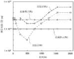
图16是示出实施例示例和比较示例的高电阻率层的薄层电阻的评估结果的图;16 is a graph showing evaluation results of sheet resistance of high-resistivity layers of Example Examples and Comparative Examples;
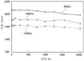
图17是示出根据实施例示例1的焦距的评估结果的图;17 is a graph showing evaluation results of focal lengths according to Embodiment Example 1;
图18是示出根据实施例示例2的焦距的评估结果的图;以及FIG. 18 is a graph showing an evaluation result of the focal length according to Embodiment Example 2; and
图19是示出根据比较示例的焦距的评估结果的图。FIG. 19 is a graph showing the evaluation result of the focal length according to the comparative example.
具体实施方式Detailed ways
在下文中,参考附图描述根据实施例的液晶光偏转装置。Hereinafter, a liquid crystal light deflection device according to an embodiment is described with reference to the accompanying drawings.
实施例1Example 1
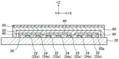
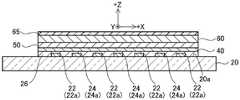
参考图1到图4描述根据本实施例的液晶光偏转装置100。如图1所示,液晶光偏转装置100包括第一基板10、第二基板20和液晶30。第一基板10包括第一电极12和配向膜15。第二基板20包括第二电极22和24、绝缘层26、高电阻率层40、第一阻挡层50、第二阻挡层60和配向膜65。高电阻率层40设置在第二电极22和24上。此外,高电阻率层40依次被第一阻挡层50和第二阻挡层60覆盖。利用液晶光偏转装置100,通过液晶30的排列中的变化产生光偏转效应。由于光偏转效应,液晶光偏转装置100作为柱状透镜作用于光。液晶光偏转装置100例如安装在液晶显示面板上。液晶光偏转装置100用作柱状透镜阵列,其在平面图像和三维图像之间切换要在液晶显示器上显示的显示图像。在本公开中,为了便于理解,图1中的液晶光偏转装置100的纵向右方向(图1的朝向右侧的方向)被定义为+X方向,向上方向(图1的朝向顶部的方向)被定义为+Z方向,并且垂直于+X和+Z方向的方向(图1的朝向前面的方向)被定义为+Y方向。The liquid crystal
第一基板10具有透明度。在本实施例中,第一基板10使可见光能够通过其中。第一基板10例如是由玻璃制成的平板基板。第一基板10和第二基板20通过密封材料70接合在一起。第一基板10和第二基板20于其间夹入液晶30。第一基板10包括第一电极12和配向膜15。The
第一基板10的第一电极12在第一基板10的第一主表面10a上由铟锡氧化物(ITO)矩形地形成。第一电极12与第二电极22的梳状齿部分22a和第二电极24的梳状齿部分24a(其在下文中进一步描述)相对。第一电极12连接到未示出的控制器。The
第一基板10的配向膜15设置在第一主表面10a和第一电极12上。配向膜15使液晶30在X方向上对齐。配向膜15例如是经受摩擦处理的聚酰亚胺配向膜。The
第二基板20与第一基板10类似,具有透明度。在本实施例中,第二基板20使可见光能够通过其中。第二基板20例如是由玻璃制成的平板基板。第二基板20与第一基板10通过密封材料70接合在一起,从而夹入液晶30。第二基板20包括两个第二电极22和24、绝缘层26、高电阻率层40、第一阻挡层50、第二阻挡层60和配向膜65。绝缘层26、高电阻率层40、第一阻挡层50和第二阻挡层60使得可见光能够通过其中。The
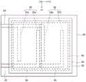
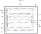
第二基板20的第二电极22和第二电极24在第二基板20的第一主表面20a上由ITO形成成为梳状齿。如图2所示,第二电极22和第二电极24分别具有梳状齿部分22a和梳状齿部分24a。梳状齿部分22a在+Y方向上延伸,并且梳状齿部分24a在-Y方向上延伸。梳状齿部分22a和梳状齿部分24a在X方向上交替地并且彼此平行地放置。The
如图1和图2所示,第二电极22和24被绝缘层26覆盖。与第一电极12类似的第二电极22和24连接到控制器。As shown in FIGS. 1 and 2 , the
如图1所示,第二基板20的绝缘层26覆盖第二电极22和24。绝缘层26将第二电极22和24与高电阻率层40绝缘。绝缘层26由氧化硅(SiO2)、氮化铝(AlN)、氮化硅(SiNX)、氟化镁(MgF2)等形成。绝缘层26例如是氧化硅膜。绝缘层26的厚度例如为50nm到1000nm。As shown in FIG. 1 , the insulating
第二基板20的高电阻率层40经由绝缘层26设置在第二电极22和24上。高电阻率层40依次被第一阻挡层50和第二阻挡层60覆盖。高电阻率层40具有例如1×10⁶Ω/sq到1×1014Ω/sq的薄层电阻值。高电阻率层40由掺杂Al的氧化锌(AZO)、氧化锌(ZnO)、铟锡(InSn)氧化物、氧化镁(MgO)等形成。高电阻率层40例如是AZO膜。例如,高电阻率层40具有20nm到500nm的厚度。The high-
第二基板20的第一阻挡层50覆盖高电阻率层40。如图1所示,第一阻挡层50优选地不仅覆盖顶表面(在+Z侧上的表面),而且覆盖高电阻率层40的侧表面。此外,第一阻挡层50优选地覆盖高电阻率层40,使得高电阻率层40的表面不从第一阻挡层50暴露。如下所述,第一阻挡层50在第二阻挡层60将形成的情况下保护高电阻率层40。The
第一阻挡层50由金属氧化物形成。金属氧化物的示例包括氧化硅、氧化铝(AlOx)、氧化钽(TaOx)、氧化铌(NbOx)、氧化钛(TiO2)、氧化锆(ZrO2)、其混合物等。第一阻挡层50例如是氧化硅膜。例如,第一阻挡层50具有10nm到500nm的厚度。The
第二基板20的第二阻挡层60覆盖第一阻挡层50和高电阻率层40。如图1所示,第二阻挡层60优选地不仅覆盖顶表面(在+Z侧上的表面)而且还覆盖第一阻挡层50的侧表面。此外,优选的是,第二阻挡层60和高电阻率层40彼此不接触。第二阻挡层60由金属氮化物或金属碳化物形成。金属氮化物和金属碳化物的示例包括氮化硅、氧氮化硅(SiON)、碳氮化硅(SiCN)、碳化硅(SiC)、其混合物等。第二阻挡层60例如是氮化硅膜。例如,第二阻挡层60具有50nm到500nm的厚度。The
第二阻挡层60保护高电阻率层40不受湿气影响,因为第二阻挡层60由具有优良防潮性能的金属氮化物或金属碳化物形成,因此可以防止或抑制高电阻率层40的恶化。在本实施例中,由于第二阻挡层60能够防止或抑制高电阻率层40的恶化,因此可以防止或抑制液晶光偏转装置100的光偏转效应(焦距)随时间而改变。当直接在高电阻率层40上形成由金属氮化物或金属碳化物形成的第二阻挡层60时,存在由于在形成第二阻挡层60中产生的分解产物(例如,氢气)而改变高电阻率层40的电阻值的风险。在本实施例中,由于第一阻挡层50覆盖高电阻率层40,因此可以防止或抑制在第二阻挡层60的成膜工艺中高电阻率层40的电阻值发生变化。此外,可以提高在液晶光偏转装置100的制造中的产量。The
第二基板20的配向膜65设置在第二阻挡层60上。与第一基板10的配向膜15类似的配向膜65使液晶30在X方向上对齐。配向膜65例如是经受摩擦处理的聚酰亚胺配向膜。The
液晶30夹在第一基板10和第二基板20之间。液晶30例如是正型向列相液晶。液晶30通过配向膜15和配向膜65在X方向上对齐。The
这里,描述了液晶光偏转装置100的操作。Here, the operation of the liquid crystal
例如,当控制器将第一基板10的第一电极12和第二基板20的第二电极22和24的电位被带到相同的电位(例如,接地电位)时,不向液晶30施加电压,因此液晶30保持在X方向上对齐。当液晶30保持在X方向上对齐时,不产生偏转效应,因此液晶光偏转装置100不作为透镜作用于光。For example, when the controller brings the potentials of the
独立地控制施加在第一基板10的第一电极12和第二基板20的第二电极22上的电压以及施加在第一基板10的第一电极12和第二基板20的第二电极24上的电压使得呈二次曲线形状的电位将形成在第一基板10和第二基板20之间。如图3所示,呈二次曲线形状形成的电位使得液晶30的分子M对齐。在液晶光偏转装置100中,液晶30的排列中的这种改变产生沿呈二次曲线形状的电位的折射率分布。在液晶光偏转装置100中,沿呈二次曲线形状的电位的折射率分布产生偏转效应。通过这样做,液晶光偏转装置100作为透镜作用于光。Independently control the voltage applied to the
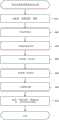
接下来,参照图4描述制造液晶光偏转装置100的方法。图4是示出液晶光偏转装置100的制造过程的流程图。液晶光偏转装置100的制造过程包括制备第一基板10和第二基板20的步骤(步骤S10)、形成绝缘层26的步骤(步骤S20)、形成高电阻率层40的步骤(步骤S30)、形成由金属氧化物形成的第一阻挡层50的步骤(步骤S40),以及形成由金属氮化物或金属碳化物形成的第二阻挡层60的步骤(步骤S50)。制造液晶光偏转装置100的方法还包括形成配向膜15和配向膜65的步骤(步骤S60),以及将第一基板10和第二基板20接合在一起并在其中注入液晶30的步骤(步骤S70)。Next, a method of manufacturing the liquid crystal
在步骤S10中,制备包括第一电极12的第一基板10和包括第二电极22和24的第二基板20。例如,通过使用溅射技术,第一电极12和第二电极22和24由ITO形成。In step S10 , the
在步骤S20中,在第二基板20的第二电极22和24上形成绝缘层26。例如,通过使用溅射技术,绝缘层26由氧化硅形成。In step S20 , an insulating
在步骤S30中,在绝缘层26上形成高电阻率层40。通过这样做,高电阻率层40通过绝缘层26设置在第二电极22和24上。例如,通过使用溅射技术,高电阻率层40由AZO形成。In step S30 , the
在步骤S40中,第一阻挡层50通过覆盖高电阻率层40形成使得高电阻率层40的表面不暴露。第一阻挡层50由金属氧化物形成。第一阻挡层50例如是由化学气相沉积(CVD)形成的氧化硅膜。在本实施例中,由于第一阻挡层50覆盖高电阻率层40,所以第一阻挡层50保护高电阻率层40免受在形成第二阻挡层60(步骤S50)期间产生的分解产物(例如,氢气)的影响,从而可以防止或抑制高电阻率层40的电阻值中的变化。因此,可以提高在液晶光偏转装置100的制造中的产量。In step S40, the
在步骤S50中,在第一阻挡层50上形成第二阻挡层60。通过这样做,高电阻率层40依次被第一阻挡层50和第二阻挡层60覆盖。第二阻挡层60由金属氮化物或金属碳化物形成。第二阻挡层60例如是由CVD形成的氮化硅膜。在本实施例中,由于第二阻挡层60覆盖高电阻率层40,所以高电阻率层40被保护不受湿气影响,因此可以防止或抑制高电阻率层40的恶化。此外,可以防止液晶光偏转装置100的光偏转效应(焦距)随时间而改变。In step S50 , a
在步骤S60中,在第一基板10的第一电极12上形成配向膜15,并且在第二阻挡层60上形成配向膜65。在步骤S60中,首先通过将聚酰亚胺材料施加到第一电极12和/或第二阻挡层60,然后通过烧制所施加的聚酰亚胺材料来形成聚酰亚胺膜。然后,通过对聚酰亚胺薄膜进行摩擦处理来形成配向膜15和65。In step S60 , the
在步骤S70中,第一基板10和第二基板20通过密封材料70经由未图示的间隔物接合在一起。然后,在第一基板10和第二基板20之间注入液晶30。如上所述,可以制造液晶光偏转装置100。In step S70 , the
如上所述,由于具有优良的防潮性能的第二阻挡层60保护高电阻率层40不受湿气影响,因此可以防止或抑制高电阻率层40的恶化,并且可以防止或抑制液晶光偏转装置100的光偏转效应(焦距)随时间而改变。另外,由于第一阻挡层50覆盖高电阻率层40,因此可以防止或抑制在第二阻挡层60的成膜工艺中高电阻率层40的电阻值发生变化。此外,可以提高在液晶光偏转装置100的制造中的产量。As described above, since the
在只有第一阻挡层50覆盖高电阻率层40的情况下,有必要增加第一阻挡层50的厚度,以保护高电阻率层40免受湿气的影响。因此,当高电阻率层40仅被第一阻挡层50覆盖时,驱动电压升高。此外,第一阻挡层50形成所花费的时间增加。在本实施例中,由于第二阻挡层60覆盖高电阻率层40,所以第一阻挡层50的厚度可以减小。因此,第一阻挡层50形成所花费的时间可以缩短。另外,可以降低液晶光偏转装置100的驱动电压。此外,通过增加第一阻挡层50和第二阻挡层60中的一个的相对介电常数,可以容易地降低液晶光偏转装置100的驱动电压。In the case where only the
实施例2Example 2
在实施例1中,虽然液晶光偏转装置100作为透镜作用于光,但是液晶光偏转装置100可以作为棱镜作用于光。In
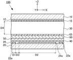
使用本实施例的液晶光偏转装置100,通过液晶30的排列中的变化来产生光偏转效应。本实施例的液晶光偏转装置100作为棱镜作用于光。在本实施例中,第二基板20的第二电极22和24以及高电阻率层40的配置与实施例1的第二基板20的第二电极22和24以及高电阻率层40的配置不同。本实施例的配置的其他方面与实施例1中的配置的其他方面类似。这里,描述第二基板20的第二电极22和24以及高电阻率层40。Using the liquid crystal
与实施例1的第二电极22和24类似的本实施例的第二基板20的第二电极22和24在第二基板20的第一主表面20a上由ITO形成成为梳状齿。第二电极22和第二电极24分别具有在+Y方向上延伸的梳状齿部分22a和在-Y方向上延伸的梳状齿部分24a。与实施例1的梳状齿部分22a和梳状齿部分24a类似的梳状齿部分22a和梳状齿部分24a在X方向上交替地并且彼此平行地放置。在本实施例中,梳状齿部分22a和梳状齿部分24a形成电极对28,并且一个电极对28的梳状齿部分22a邻近另一个电极对28的梳状齿部分24a放置,如图5和图6所示。在图6中,为了便于理解,省略了绝缘层26。The
在本实施例中,第二基板20包括两个高电阻率层40,如图5和图6所示。高电阻率层40中的每个通过绝缘层26设置在一个电极对28(第二电极22的梳状齿部分22a和第二电极24的梳状齿部分24a)上。In this embodiment, the
接下来,描述本实施例的液晶光偏转装置100的操作。Next, the operation of the liquid crystal
与实施例1的液晶光偏转装置100类似,当第一基板10的第一电极12和第二基板20的第二电极22和24的电位被带到相同的电位(例如,接地电位)时,液晶30保持在X方向上对齐。当液晶30保持在X方向上对齐时,不产生偏转效应,因此液晶光偏转装置100不作为棱镜作用于光。Similar to the liquid crystal
独立地控制施加在第一基板10的第一电极12和第二基板20的第二电极22上的电压以及施加在第一基板10的第一电极12和第二基板20的第二电极24上的电压导致一个电极对28的梳状齿部分22a和梳状齿部分24a之间的电位梯度将形成。例如,假设第一电极12为接地电位(0V),则向第二电极22施加第一电压,并向第二电极24施加大于第一电压的第二电压。在这种情况下,在一个电极对28的梳状齿部分22a和梳状齿部分24a之间形成线性电位梯度,因为高电阻率层40经由绝缘层26设置在一个电极对28上。由于形成的线性电位梯度,所以液晶30的分子M如图7所示对齐。液晶30的排列中的这种变化产生线性折射率梯度。因此,液晶光偏转装置100折射从第一基板10或第二基板20入射的光。即,本实施例的液晶光偏转装置100作为棱镜作用于光。Independently control the voltage applied to the
如上所述,在本实施例的液晶光偏转装置100中,通过液晶30的排列中的变化产生光偏转效应。本实施例的液晶光偏转装置100作为棱镜对光起作用。此外,与实施例1中的类似,由于具有优良的防潮性能的第二阻挡层60保护高电阻率层40免受湿气的影响,因此可以防止或抑制高电阻率层40的恶化,并且可以防止或抑制液晶光偏转装置100的光偏转效应(偏转角度或折射角度)随时间变化。由于第一阻挡层50覆盖高电阻率层40,因此可以防止或抑制在第二阻挡层60的成膜工艺中高电阻率层40的电阻值发生变化。此外,可以提高在液晶光偏转装置100的制造中的产量。此外,与实施例1中的相似,第一阻挡层50形成所花费的时间可以缩短,并且可以降低液晶光偏转装置100的驱动电压。As described above, in the liquid crystal
修改的示例Modified example
在不脱离本公开的要旨的情况下,可以以各种方式修改上述实施例。The above-described embodiments may be modified in various ways without departing from the gist of the present disclosure.
在实施例1和实施例2中,设置在第二基板20的第二电极22和24上的高电阻率层40依次被第一阻挡层50和第二阻挡层60覆盖。只要高电阻率层40设置在第一基板10的第一电极12或第二基板20的第二电极22和24中的至少一个上,并且依次被第一阻挡层50和第二阻挡层60覆盖就足够了。例如,如图8所示,设置在第一电极12上的高电阻率层40和设置在第二电极22和24上的高电阻率层40每个可以依次被第一阻挡层50和第二阻挡层60覆盖。In
将设置在第一基板10和第二基板20上的电极可以是任何形状。例如,实施例1的第二基板20可以包括设置有如图9所示的开口72a的第二电极72,而不是第二电极22和24。在这种情况下,液晶光偏转装置100作为一个凸透镜或一个凹透镜作用于光。The electrodes to be provided on the
此外,实施例1的第一基板10可以包括形如图10所示的梳状齿的两个第一电极74和76,以代替第一电极12。第一电极74和第一电极76分别包括梳状齿部分74a和梳状齿部分76a。高电阻率层40设置在第一电极74和76上。此外,高电阻率层40依次被第一阻挡层50和第二阻挡层60覆盖。在这种情况下,液晶光偏转装置100作为微透镜作用于光。此外,该液晶光偏转装置100还作为能够在两个方向上切换偏转方向的柱状透镜起作用。In addition, the
如图11所示,实施例1的高电阻率层40可以划分成几个部分。在实施例2中,一个高电阻率层40可以通过绝缘层26设置在两个电极对28上。此外,如图12所示,第一阻挡层50和第二阻挡层60不必覆盖高电阻率层40的侧表面。As shown in FIG. 11 , the high-
虽然第二电极22和24设置在第二基板20的第一主表面20a上,但是第二电极22和24可以形成在设置在第二基板20的第一主表面20a上的第三阻挡层80上,如图13所示。与第二阻挡层60类似的第三阻挡层80由金属氮化物或金属碳化物形成。通过这样做,即使第二基板20是湿气容易通过的基板(例如,塑料基板),也可以保护高电阻率层40。Although the
在实施例1和实施例2中,虽然配向膜15和65使得液晶30在X方向上对齐,但是配向膜15和65使得液晶30对齐的方向不限于X方向。只要实施例1和实施例2的配向膜15和65使液晶30处于均匀排列就足够了。例如,配向膜15和65可使液晶30在Y方向上对齐。In Example 1 and Example 2, although the
虽然上述描述了优选实施例的一些示例,但这一详细描述不是限制性的,并且本发明的范围仅由包括的权利要求以及这些权利要求有权获得的等效物的完整范围限定。While some examples of preferred embodiments have been described above, this detailed description is not to be limiting, and the scope of the invention is defined only by the appended claims, along with the full scope of equivalents to which such claims are entitled.
实施例示例Example of an embodiment
虽然下面的实施例示例更详细地描述了本公开,但是应以说明性意义而不是限制性意义来看待实施例示例。While the following examples of embodiment describe the present disclosure in more detail, the examples of embodiment are to be regarded in an illustrative rather than a restrictive sense.
作为实施例示例,创建了图14所示的实施例1的液晶光偏转装置100。在所创建的液晶光偏转装置100上进行高温和高湿度评估。具体地,将所创建的液晶光偏转装置100暴露于60℃和90%湿度的环境中,持续预定时间段,然后测量高电阻率层40的薄层电阻和液晶光偏转装置100的焦距。此外,作为比较示例,创建了液晶光偏转装置,其具有与实施例的配置类似的配置,除了不具有第一阻挡层50和第二阻挡层60之外。以与实施例示例的方式类似的方式对比较示例的液晶光偏转装置进行高温和高湿度评估。As an embodiment example, the liquid crystal
在图15中示出了实施例示例的液晶光偏转装置100和比较示例的液晶光偏转装置的层的厚度和构成层的材料。The thicknesses of the layers and the materials constituting the layers of the liquid crystal
实施例示例1的液晶光偏转装置100和实施例示例2的液晶光偏转装置100具有包括在高电阻率层40中的AZO的不同组成比。同样地,比较示例1的液晶光偏转装置100和比较示例2的液晶光偏转装置100具有包括在高电阻率层40中的AZO的不同组成比。The liquid crystal
此外,第二电极22的梳状齿部分22a的宽度D1被设置为10μm,并且第二电极24的梳状齿部分24a的宽度D2被设置为116.9μm。此外,梳状齿部分22a和梳状齿部分24a之间的间隔D3被设置为10μm。此外,液晶30的厚度D4被设置为20μm。Further, the width D1 of the comb-shaped
在从1Hz到1500Hz的频率处,当在第一电极12和第二电极22的梳状齿部分22上应用5V的电压以及在第一电极12和第二电极24的梳状齿部分24a上应用1.5V的电压时测量焦距。At frequencies from 1 Hz to 1500 Hz, when a voltage of 5V is applied to the comb-shaped
接下来,描述了实施例示例的液晶光偏转装置100和比较示例的液晶光偏转装置100的评估结果。Next, the evaluation results of the liquid crystal
图16示出了实施例示例和比较示例中高电阻率层40的薄层电阻的评估示例。如图16所示,实施例示例1和2中的液晶光偏转装置100中的高电阻率层40的薄层电阻即使在60℃和90%湿度的环境中暴露不少于2000个小时也不发生变化。相反,比较示例1和2中的液晶光偏转装置中的高电阻率层40的薄层电阻上下变化很大。因此,可以通过由金属氧化物形成的第一阻挡层50和由金属氮化物或金属碳化物形成的第二阻挡层60依次覆盖高电阻率层40来防止或抑制高电阻率层40的恶化。FIG. 16 shows an evaluation example of the sheet resistance of the high-
图17是示出实施例示例1的液晶光偏转装置100中的焦距的评估结果的图。图18示出了实施例示例2的液晶光偏转装置100中的焦距的评估结果。此外,图19示出了比较示例1和2的液晶光偏转装置100中的焦距的评估结果。FIG. 17 is a diagram showing an evaluation result of the focal length in the liquid crystal
如图17和18所示,使用实施例1和2的液晶光偏转装置100,即使在60℃和90%湿度的环境中暴露不少于2000个小时,焦距也保持基本相同。相反地,如图19所示,使用比较示例1和2的液晶光偏转装置,焦距变化不超过300μm。因此,由金属氧化物形成的第一阻挡层50和由金属氮化物或金属碳化物形成的第二阻挡层60依次覆盖高电阻率层40可以防止或抑制液晶光偏转装置100的焦距随时间变化。也就是说,这可以防止或抑制光偏转效应随时间变化。图19示出了在相同频率下可测量的焦距,因为可以测量焦距的频率随着比较示例1和2的液晶光偏转装置而改变。As shown in FIGS. 17 and 18 , using the liquid crystal
如上所述,由金属氧化物形成的第一阻挡层50和由金属氮化物或金属碳化物形成的第二阻挡层60依次覆盖高电阻率层40可以防止或抑制高电阻率层40的恶化,并且可以防止或抑制液晶光偏转装置100的光偏转效应随时间变化。As described above, the
为了解释的目的,前面描述了一些示例实施例。虽然前面的讨论已经呈现了具体的实施例,但是本领域技术人员将认识到,在不脱离本发明的更广泛的精神和范围的情况下,可以在形式和细节上进行改变。因此,说明书和附图将被视为说明性的而非限制性的。因此,不应在限制性意义上理解该详细描述,并且本发明的范围仅由包括的权利要求以及这些权利要求有权获得的等效物的完整范围限定。For purposes of explanation, some example embodiments have been described above. Although the foregoing discussion has presented specific embodiments, workers skilled in the art will recognize that changes may be made in form and detail without departing from the broader spirit and scope of the invention. Accordingly, the specification and drawings are to be regarded in an illustrative rather than a restrictive sense. Therefore, this detailed description is not to be taken in a limiting sense, and the scope of the invention is defined only by the appended claims, along with the full scope of equivalents to which such claims are entitled.
Claims (7)
Applications Claiming Priority (2)
| Application Number | Priority Date | Filing Date | Title |
|---|---|---|---|
| JP2019236025AJP7356899B2 (en) | 2019-12-26 | 2019-12-26 | Liquid crystal light deflection element and method for manufacturing the liquid crystal light deflection element |
| JP2019-236025 | 2019-12-26 |
Publications (2)
| Publication Number | Publication Date |
|---|---|
| CN113050333Atrue CN113050333A (en) | 2021-06-29 |
| CN113050333B CN113050333B (en) | 2024-12-10 |
Family
ID=76507956
Family Applications (1)
| Application Number | Title | Priority Date | Filing Date |
|---|---|---|---|
| CN202011504315.1AActiveCN113050333B (en) | 2019-12-26 | 2020-12-18 | Liquid crystal light deflection device and method for manufacturing liquid crystal light deflection device |
Country Status (3)
| Country | Link |
|---|---|
| US (1) | US11422414B2 (en) |
| JP (1) | JP7356899B2 (en) |
| CN (1) | CN113050333B (en) |
Cited By (1)
| Publication number | Priority date | Publication date | Assignee | Title |
|---|---|---|---|---|
| CN117083566A (en)* | 2022-11-01 | 2023-11-17 | 成都耶塔科技有限责任公司 | Liquid crystal optical device, liquid crystal lens array, electronic product and manufacturing method |
Families Citing this family (1)
| Publication number | Priority date | Publication date | Assignee | Title |
|---|---|---|---|---|
| US12242159B2 (en)* | 2022-07-25 | 2025-03-04 | Meta Platforms Technologies, Llc | Optical devices with active components coupled with passive components |
Citations (4)
| Publication number | Priority date | Publication date | Assignee | Title |
|---|---|---|---|---|
| JPH02179615A (en)* | 1988-12-29 | 1990-07-12 | Oki Electric Ind Co Ltd | Liquid crystal display device |
| JP2014032313A (en)* | 2012-08-03 | 2014-02-20 | Nippon Electric Glass Co Ltd | Method of producing liquid crystal element, and liquid crystal element |
| CN103890646A (en)* | 2011-10-25 | 2014-06-25 | 日本电气硝子株式会社 | Liquid crystal element and cell for liquid crystal element |
| JP2016062100A (en)* | 2014-09-12 | 2016-04-25 | 三星ディスプレイ株式會社Samsung Display Co.,Ltd. | Optical system having contact sensing function, and display device including the same |
Family Cites Families (8)
| Publication number | Priority date | Publication date | Assignee | Title |
|---|---|---|---|---|
| US20060153997A1 (en)* | 2005-01-07 | 2006-07-13 | Eastman Kodak Company | Method of varying wavelengths of liquid crystals |
| JP5334116B2 (en) | 2009-07-07 | 2013-11-06 | 秋田県 | Low voltage liquid crystal lens |
| CN104157222B (en)* | 2009-12-10 | 2018-11-06 | 三菱化学株式会社 | Surface protection panel and liquid crystal image display device |
| TW201423236A (en)* | 2012-12-11 | 2014-06-16 | Wintek Corp | 2D and 3D switchable display device and liquid crystal lenticular lens thereof |
| CN103018990B (en)* | 2012-12-14 | 2015-12-02 | 京东方科技集团股份有限公司 | A kind of array base palte and its preparation method and liquid crystal indicator |
| WO2015168769A1 (en)* | 2014-05-05 | 2015-11-12 | Lensvector Inc. | Tunable liquid crystal optical device |
| WO2016009715A1 (en)* | 2014-07-16 | 2016-01-21 | 株式会社Joled | Transistor, display device, and electronic apparatus |
| KR102145930B1 (en)* | 2015-01-23 | 2020-08-19 | 시부야,기이찌 | Liquid crystal devices, deflection devices, liquid crystal modules and electronic devices |
- 2019
- 2019-12-26JPJP2019236025Apatent/JP7356899B2/enactiveActive
- 2020
- 2020-12-18USUS17/126,137patent/US11422414B2/enactiveActive
- 2020-12-18CNCN202011504315.1Apatent/CN113050333B/enactiveActive
Patent Citations (4)
| Publication number | Priority date | Publication date | Assignee | Title |
|---|---|---|---|---|
| JPH02179615A (en)* | 1988-12-29 | 1990-07-12 | Oki Electric Ind Co Ltd | Liquid crystal display device |
| CN103890646A (en)* | 2011-10-25 | 2014-06-25 | 日本电气硝子株式会社 | Liquid crystal element and cell for liquid crystal element |
| JP2014032313A (en)* | 2012-08-03 | 2014-02-20 | Nippon Electric Glass Co Ltd | Method of producing liquid crystal element, and liquid crystal element |
| JP2016062100A (en)* | 2014-09-12 | 2016-04-25 | 三星ディスプレイ株式會社Samsung Display Co.,Ltd. | Optical system having contact sensing function, and display device including the same |
Cited By (1)
| Publication number | Priority date | Publication date | Assignee | Title |
|---|---|---|---|---|
| CN117083566A (en)* | 2022-11-01 | 2023-11-17 | 成都耶塔科技有限责任公司 | Liquid crystal optical device, liquid crystal lens array, electronic product and manufacturing method |
Also Published As
| Publication number | Publication date |
|---|---|
| US11422414B2 (en) | 2022-08-23 |
| CN113050333B (en) | 2024-12-10 |
| JP7356899B2 (en) | 2023-10-05 |
| JP2021105648A (en) | 2021-07-26 |
| US20210200041A1 (en) | 2021-07-01 |
Similar Documents
| Publication | Publication Date | Title |
|---|---|---|
| US8897614B2 (en) | Electro-optical element | |
| CN101558370B (en) | Substrate for display panel, display panel, display device, and manufacturing method of substrate for display panel | |
| US9239484B2 (en) | Display device substrate and method for fabricating same, and display device | |
| US20210231978A1 (en) | Liquid Crystal Lens and Liquid Crystal Glasses | |
| CN113050333B (en) | Liquid crystal light deflection device and method for manufacturing liquid crystal light deflection device | |
| JP6377408B2 (en) | Polarizing plate and liquid crystal display device including the same | |
| US20120194898A1 (en) | E-paper display device and method for manufacturing the same | |
| US20110102732A1 (en) | Method for manufacturing liquid crystal display device | |
| KR102666083B1 (en) | Touch sensitive device and display device comprising the same | |
| JP2010026079A (en) | Optical device | |
| JPWO2009084692A1 (en) | Variable focus lens | |
| KR102062243B1 (en) | Thin film transistor and image display apparatus | |
| JP2009122474A (en) | Liquid crystal display device and manufacturing method thereof | |
| US9529243B2 (en) | Liquid crystal element and cell for liquid crystal element | |
| JP5360256B2 (en) | Optical waveguide device | |
| US10600978B2 (en) | Liquid crystal element and light control apparatus for accurate light control | |
| US20140267965A1 (en) | Optical deflector | |
| JP6507311B2 (en) | Substrate with transparent conductive layer and liquid crystal panel | |
| US10168781B2 (en) | Touch sensitive device and display device including the same | |
| US10528202B2 (en) | Piezoelectric sensor, touch panel, touch input device, and display device | |
| JP5411089B2 (en) | Variable focus lens | |
| CN103003744B (en) | Liquid-crystal display device and method of manufacturing same | |
| JP6019903B2 (en) | Method for manufacturing liquid crystal element and liquid crystal element | |
| WO2013080819A1 (en) | Liquid-crystal lens | |
| TW201500824A (en) | Liquid crystal lens |
Legal Events
| Date | Code | Title | Description |
|---|---|---|---|
| PB01 | Publication | ||
| PB01 | Publication | ||
| SE01 | Entry into force of request for substantive examination | ||
| SE01 | Entry into force of request for substantive examination | ||
| GR01 | Patent grant | ||
| GR01 | Patent grant |