CN112880657B - System-on-a-chip for signal demodulation and control of MEMS resonant gyroscope - Google Patents
System-on-a-chip for signal demodulation and control of MEMS resonant gyroscopeDownload PDFInfo
- Publication number
- CN112880657B CN112880657BCN202110053102.XACN202110053102ACN112880657BCN 112880657 BCN112880657 BCN 112880657BCN 202110053102 ACN202110053102 ACN 202110053102ACN 112880657 BCN112880657 BCN 112880657B
- Authority
- CN
- China
- Prior art keywords
- module
- chip
- signal
- bus
- processor
- Prior art date
- Legal status (The legal status is an assumption and is not a legal conclusion. Google has not performed a legal analysis and makes no representation as to the accuracy of the status listed.)
- Active
Links
Images


Classifications
- G—PHYSICS
- G01—MEASURING; TESTING
- G01C—MEASURING DISTANCES, LEVELS OR BEARINGS; SURVEYING; NAVIGATION; GYROSCOPIC INSTRUMENTS; PHOTOGRAMMETRY OR VIDEOGRAMMETRY
- G01C19/00—Gyroscopes; Turn-sensitive devices using vibrating masses; Turn-sensitive devices without moving masses; Measuring angular rate using gyroscopic effects
- G01C19/56—Turn-sensitive devices using vibrating masses, e.g. vibratory angular rate sensors based on Coriolis forces
- G01C19/5776—Signal processing not specific to any of the devices covered by groups G01C19/5607 - G01C19/5719
Landscapes
- Engineering & Computer Science (AREA)
- Physics & Mathematics (AREA)
- General Physics & Mathematics (AREA)
- Radar, Positioning & Navigation (AREA)
- Remote Sensing (AREA)
- Signal Processing (AREA)
- Gyroscopes (AREA)
Abstract
Translated fromChinese
Description
Translated fromChinese技术领域technical field
本发明涉及一种传感器检测与集成电路技术领域,特别是关于一种用于MEMS谐振式陀螺仪信号解调及控制的片上系统。The invention relates to the field of sensor detection and integrated circuit technology, in particular to an on-chip system for signal demodulation and control of a MEMS resonant gyroscope.
背景技术Background technique
精密测量仪器信号处理及控制是对高仪器性能表现的重要手段,也是传感器领域科学研究的重要方面。其中,MEMS谐振式陀螺仪大量存在于以惯性导航制造业为代表的工业生产和科学实践中,其具有体积小、重量轻、功耗低、价格低、环境适应性强等特点,广泛应用于航空航天、汽车等领域。Signal processing and control of precision measuring instruments is an important means of high instrument performance and an important aspect of scientific research in the field of sensors. Among them, MEMS resonant gyroscopes are widely used in industrial production and scientific practice represented by the inertial navigation manufacturing industry. They are characterized by small size, light weight, low power consumption, low price, and strong environmental adaptability. aerospace, automotive and other fields.
MEMS谐振式陀螺仪一般有两种工作模式:驱动模式和检测模式。驱动轴在驱动力的作用下产生谐振运动。在科式力的作用下,检测轴也会产生谐振运动。需要检测的角速度信息包含在检测轴的输出幅度。为了获得大的振幅提高分辨率时,驱动轴通常在谐振频率下振动,带宽相对较窄。在大气条件下,需要使驱动轴的信号保持振幅稳定性,这需要检测和控制陀螺驱动轴的振动相位和频率。为了防止检测轴运动的耦合,需要对检测轴添加平衡力使检测轴保持静止,这也需要对检测轴的振动相位和频率进行检测和控制。常见的检测和控制方案是使用分立器件,如AD/DA芯片,结合MCU、DSP等在软件环境中完成计算。这种方案存在信号传输损失问题,计算实时性问题和功耗问题,同时分立器件的存在限制了整个传感器测控系统集成度的进一步提高。MEMS resonant gyroscope generally has two working modes: drive mode and detection mode. The drive shaft generates resonant motion under the action of the driving force. Under the action of Coriolis force, the detection shaft will also produce resonant motion. The angular velocity information to be detected is contained in the output amplitude of the detection axis. In order to obtain large amplitude and improve resolution, the drive shaft usually vibrates at the resonant frequency with a relatively narrow bandwidth. Amplitude stability of the drive shaft signal is required under atmospheric conditions, which requires detection and control of the vibration phase and frequency of the gyro drive shaft. In order to prevent the coupling of the motion of the detection shaft, it is necessary to add a balance force to the detection shaft to keep the detection shaft stationary, which also requires detection and control of the vibration phase and frequency of the detection shaft. A common detection and control scheme is to use discrete devices, such as AD/DA chips, combined with MCU, DSP, etc. to complete calculations in a software environment. This solution has the problem of signal transmission loss, real-time calculation and power consumption. At the same time, the existence of discrete devices limits the further improvement of the integration of the entire sensor measurement and control system.
发明内容Contents of the invention
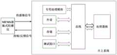
针对上述问题,本发明的目的是提供一种用于MEMS谐振式陀螺仪信号解调及控制的片上系统,其能够实现单个芯片完成所有数字和模拟测控电路,进行陀螺信号的处理,以实现陀螺驱动轴和检测轴信号的控制。For the problems referred to above, the object of the present invention is to provide a system-on-chip for MEMS resonant gyroscope signal demodulation and control, which can realize a single chip to complete all digital and analog measurement and control circuits, and carry out the processing of gyroscope signals to realize gyroscope Control of drive axis and detection axis signals.
为实现上述目的,本发明采取以下技术方案:一种用于MEMS谐振式陀螺仪信号解调及控制的片上系统,其包括:处理器、专用处理模块、存储加载模块、外设、调试接口和总线;MEMS谐振式陀螺仪经A/D模块将传感器信号传输至所述处理器,所述处理器经所述总线分别与所述专用处理模块、存储加载模块、外设和调试接口进行信息交互;所述处理器将接收到的数据处理后经所述A/D模块向所述MEMS谐振式陀螺仪传输控制和反馈信号。To achieve the above object, the present invention takes the following technical solutions: a system-on-chip for MEMS resonant gyroscope signal demodulation and control, which includes: processor, special processing module, storage loading module, peripheral hardware, debugging interface and Bus; the MEMS resonant gyroscope transmits sensor signals to the processor through the A/D module, and the processor performs information interaction with the dedicated processing module, storage loading module, peripherals and debugging interface respectively through the bus ; The processor processes the received data and transmits control and feedback signals to the MEMS resonant gyroscope via the A/D module.
进一步,所述总线包括用于和处理器通信的高速AHB总线、总线转接模块和用于驱动低速设备的APB总线,所述AHB总线和APB总线通过所述总线转接模块完成信号的传输;Further, the bus includes a high-speed AHB bus for communicating with the processor, a bus transfer module, and an APB bus for driving low-speed devices, and the AHB bus and the APB bus complete signal transmission through the bus transfer module;
所述专用处理模块包括挂载在所述AHB总线上的正余弦计算模块和挂载在所述APB总线上的LMSD解算模块;所述正余弦计算模块用于计算输入角度信号的正弦值和余弦值;所述LMSD解算模块用于解算陀螺信号,解算出来自陀螺驱动轴和检测轴信号的幅值和相位信息,传输至所述处理器中,用于在所述处理器中运行闭环控制程序;The dedicated processing module includes a sine and cosine calculation module mounted on the AHB bus and an LMSD solving module mounted on the APB bus; the sine and cosine calculation module is used to calculate the sine value and the input angle signal Cosine value; the LMSD calculation module is used to solve the gyro signal, solve the amplitude and phase information from the gyro drive axis and the detection axis signal, and transmit it to the processor for running in the processor Closed-loop control program;
所述外设包括挂载在所述APB总线上的AD/DA驱动器、PLL模块、通用GPIO、UART模块、OTP驱动模块和SPI接口模块;所述PLL模块用于配置系统时钟,所述AD/DA模块是驱动ADI的AD7690和DAC8812芯片的驱动接口电路;The peripheral hardware includes an AD/DA driver, a PLL module, a general-purpose GPIO, a UART module, an OTP driver module and an SPI interface module mounted on the APB bus; the PLL module is used to configure the system clock, and the AD/DA The DA module is the driver interface circuit that drives ADI's AD7690 and DAC8812 chips;
所述存储加载模块包括片上一次性可编程存储OTP及片上静态随机读写存储器SRAM;所述SRAM的驱动模块挂载在所述AHB总线上,所述OTP的驱动模块挂载在所述APB总线上,同时所述APB总线上挂载片外FLASH的驱动模块,用于读写片外部FLASH存储器。The storage loading module includes on-chip one-time programmable storage OTP and on-chip static random read-write memory SRAM; the driver module of the SRAM is mounted on the AHB bus, and the driver module of the OTP is mounted on the APB bus At the same time, an off-chip FLASH driver module is mounted on the APB bus for reading and writing the off-chip FLASH memory.
进一步,所述PLL模块是一个数字和模拟混合的电路模块,能接收外部两个晶振的时钟信号并选择其一作为输入时钟,PLL内部对时钟进行预分频,倍频和两次后分频,输出用于驱动时钟信号。Further, the PLL module is a digital and analog mixed circuit module, which can receive the clock signals of two external crystal oscillators and select one of them as the input clock. The PLL internally performs pre-division, frequency multiplication and post-division twice on the clock. , the output is used to drive the clock signal.
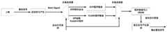
进一步,所述存储加载模块由存储器和程序加载模块构成,所述存储器用于存储运行于处理其中的程序,所述程序加载模块用于加载程序,其加载的程序数据来源于片上的OTP存储、片外的FLASH存储或JTAG加载。Further, the storage loading module is composed of a memory and a program loading module, the memory is used to store the program running in the process, the program loading module is used to load the program, and the loaded program data comes from the on-chip OTP storage, Off-chip FLASH storage or JTAG loading.
进一步,所述程序加载方式通过片上引脚的高低电平进行控制,根据高低电平的不同读取不同存储的数据,将程序数据再写入到片上的SRAM,最后重新进行系统的复位并开始执行程序。Further, the program loading method is controlled by the high and low levels of the on-chip pins, reads different stored data according to the difference in high and low levels, rewrites the program data into the on-chip SRAM, and finally resets the system and starts execute program.
进一步,所述LMSD解算模块输出的信号解调结果包含同相分量和正交分量;待解调的信号、参考正弦和余弦信号输入所述LMSD解算模块内,解调结果在系统复位时会被赋予初值,在解调过程中,解调结果组成的向量与参考信号组成的向量进行点积操作,并和待解调信号做减法,获得误差计算值,误差计算值乘上增益系数,并分别乘上两个参考信号,作为解调结果的增量值;解调结果与增量值做加法完成解调结果的更新。Further, the signal demodulation result output by the LMSD resolution module includes an in-phase component and a quadrature component; the signal to be demodulated, the reference sine and cosine signals are input in the LMSD resolution module, and the demodulation result will be reset when the system is reset Given the initial value, in the demodulation process, the vector composed of the demodulation result and the vector composed of the reference signal are subjected to a dot product operation, and subtracted from the signal to be demodulated to obtain the error calculation value, which is multiplied by the gain coefficient, The two reference signals are respectively multiplied as the incremental value of the demodulation result; the demodulation result is added to the incremental value to complete the update of the demodulation result.
进一步,所述正余弦计算模块采用查表插值的方式实现单个时钟周期完成正弦和余弦的计算。Further, the sine and cosine calculation module uses a look-up table interpolation method to complete the calculation of sine and cosine in a single clock cycle.
进一步,所述正余弦计算模块包含AHB总线上的单周期高速计算模块和APB总线上的低功耗计算模块;所述单周期高速计算模块采用查表插值法根据输入角度信号,计算正弦值和余弦值;所述低功耗计算模块基于Cordic算法实现,并使用28级流水线实现。Further, the sine-cosine calculation module includes a single-cycle high-speed calculation module on the AHB bus and a low-power calculation module on the APB bus; the single-cycle high-speed calculation module uses a look-up table interpolation method to calculate the sine value and the input angle signal. Cosine value; the low-power calculation module is implemented based on the Cordic algorithm, and is implemented using a 28-stage pipeline.
进一步,所述处理器采用ARM的32位Cortex-M3处理器核。Further, the processor adopts a 32-bit Cortex-M3 processor core of ARM.
进一步,所述调试接口采用JTAG接口。Further, the debugging interface adopts a JTAG interface.
本发明由于采取以上技术方案,其具有以下优点:1、本发明进行传感器测控时,不仅可以用于MEMS谐振式陀螺仪的驱动控制和信号检测,也可以使用片上的AD/DA驱动模块兼容其他传感器,提高了测控系统对传感器的兼容性和灵活性。2、本发明的片上系统包含低功耗通过处理器和专用处理模块,通过电路参数配置,提高了处理电路的灵活性。处理器的存在使得系统可以执行复杂的算法进行信号处理,提高了系统的环境适应性。3、本发明采用的数模混合PLL可以动态调整系统时钟频率,便于进行速度和功耗的实时调整。4、本发明采用的程序加载模块,可以面向在线调试,片内启动、片外启动三种工作方式,提高了工作方式的灵活性。因此,本发明可以广泛应用于MEMS谐振式陀螺仪的信号解调及控制领域。Because the present invention adopts the above technical scheme, it has the following advantages: 1. When the present invention performs sensor measurement and control, it can not only be used for the drive control and signal detection of the MEMS resonant gyroscope, but also can use the AD/DA drive module on the chip to be compatible with other Sensors improve the compatibility and flexibility of the measurement and control system for sensors. 2. The system-on-a-chip of the present invention includes a low-power passthrough processor and a dedicated processing module, and improves the flexibility of the processing circuit through circuit parameter configuration. The existence of the processor enables the system to execute complex algorithms for signal processing, which improves the environmental adaptability of the system. 3. The digital-analog hybrid PLL adopted in the present invention can dynamically adjust the system clock frequency, which is convenient for real-time adjustment of speed and power consumption. 4. The program loading module adopted by the present invention can be oriented to online debugging, and has three working modes of on-chip startup and off-chip startup, which improves the flexibility of the working mode. Therefore, the present invention can be widely used in the field of signal demodulation and control of MEMS resonant gyroscopes.
附图说明Description of drawings
图1是本发明的测控系统整体架构框图;Fig. 1 is a block diagram of the overall architecture of the measurement and control system of the present invention;
图2是本发明的模块和总线架构框图;Fig. 2 is a block diagram of a module and a bus architecture of the present invention;
图3是本发明实施例程序从存储中加载的两种方式;Fig. 3 shows two ways of loading the program from storage in the embodiment of the present invention;
图4是本发明实施例陀螺闭环控制工作原理;Fig. 4 is the operating principle of the gyro closed-loop control of the embodiment of the present invention;
图5是本发明实施例LMSD解算模块工作原理;Fig. 5 is the operating principle of the LMSD solution module of the embodiment of the present invention;
图6是本发明实施例查表插值正余弦计算模块工作原理。Fig. 6 is the working principle of the table look-up interpolation sine and cosine calculation module according to the embodiment of the present invention.
具体实施方式Detailed ways
为使本发明实施例的目的、技术方案和优点更加清楚,下面将结合本发明实施例的附图,对本发明实施例的技术方案进行清楚、完整地描述。显然,所描述的实施例是本发明的一部分实施例,而不是全部的实施例。基于所描述的本发明的实施例,本领域普通技术人员所获得的所有其他实施例,都属于本发明保护的范围。In order to make the purpose, technical solutions and advantages of the embodiments of the present invention more clear, the following will clearly and completely describe the technical solutions of the embodiments of the present invention in conjunction with the drawings of the embodiments of the present invention. Apparently, the described embodiments are some, not all, embodiments of the present invention. All other embodiments obtained by those skilled in the art based on the described embodiments of the present invention belong to the protection scope of the present invention.
在本发明的描述中,需要理解的是,术语“上”、“下”“内”、“外”等指示的方位或位置关系为基于附图所示的方位或位置关系,仅是为了便于描述本发明和简化描述,而不是指示或暗示所指的装置或元件必须具有特定的方位、以特定的方位构造和操作,因此不能理解为对本发明的限制。In the description of the present invention, it should be understood that the orientation or positional relationship indicated by the terms "upper", "lower", "inner", "outer" and so on is based on the orientation or positional relationship shown in the drawings, and is only for convenience The present invention is described and simplified descriptions do not indicate or imply that the device or element referred to must have a specific orientation, be constructed and operate in a specific orientation, and thus should not be construed as limiting the present invention.
下面结合附图和实施例对本发明进行详细的描述。The present invention will be described in detail below in conjunction with the accompanying drawings and embodiments.
如图1所示,本发明提出的一种用于MEMS谐振式陀螺仪信号解调及控制的片上系统,其包括处理器、专用处理模块、存储加载模块、外设、调试接口和总线。MEMS谐振式陀螺仪经A/D模块将传感器信号传输至处理器,处理器经总线分别与专用处理模块、存储加载模块、外设和调试接口进行信息交互。处理器将接收到的数据处理后经A/D模块向MEMS谐振式陀螺仪传输控制和反馈信号。As shown in Figure 1, a system-on-a-chip for MEMS resonant gyroscope signal demodulation and control proposed by the present invention includes a processor, a dedicated processing module, a storage loading module, peripherals, a debugging interface and a bus. The MEMS resonant gyroscope transmits the sensor signal to the processor through the A/D module, and the processor performs information interaction with the dedicated processing module, storage loading module, peripherals and debugging interface through the bus. The processor processes the received data and transmits control and feedback signals to the MEMS resonant gyroscope through the A/D module.
在一个优选的实施例中,处理器采用ARM的32位Cortex-M3处理器核。In a preferred embodiment, the processor adopts ARM's 32-bit Cortex-M3 processor core.
如图2所示,总线包括用于和处理器通信的高速AHB总线、总线转接模块和用于驱动低速设备的APB总线,AHB总线和APB总线通过总线转接模块完成信号的传输。As shown in Figure 2, the bus includes a high-speed AHB bus for communicating with the processor, a bus adapter module, and an APB bus for driving low-speed devices. The AHB bus and the APB bus complete signal transmission through the bus adapter module.
专用处理模块包括挂载在AHB总线上的正余弦计算模块和挂载在APB总线上的LMSD解算模块。正余弦计算模块用于计算输入角度信号的正弦值和余弦值;LMSD解算模块用于解算陀螺信号,解算出来自陀螺驱动轴和检测轴信号的幅值和相位信息,传输至处理器中,用于在处理器中运行闭环控制程序。The special processing module includes the sine and cosine calculation module mounted on the AHB bus and the LMSD calculation module mounted on the APB bus. The sine and cosine calculation module is used to calculate the sine and cosine values of the input angle signal; the LMSD calculation module is used to calculate the gyro signal, and calculate the amplitude and phase information from the gyro drive axis and detection axis signals, and transmit them to the processor , used to run the closed-loop control program in the processor.
外设包括挂载在APB总线上的AD/DA驱动器、PLL模块、通用GPIO、UART模块、OTP驱动模块和SPI接口模块。其中,PLL模块用于配置系统时钟,PLL模块是一个数字和模拟混合的电路模块,可以接收外部两个晶振的时钟信号并选择其一作为输入时钟,PLL内部对时钟进行预分频,倍频和两次后分频,输出用于驱动时钟信号;AD/DA模块是驱动ADI的AD7690和DAC8812芯片的驱动接口电路。Peripherals include AD/DA driver, PLL module, general GPIO, UART module, OTP driver module and SPI interface module mounted on the APB bus. Among them, the PLL module is used to configure the system clock. The PLL module is a digital and analog circuit module that can receive clock signals from two external crystal oscillators and select one of them as the input clock. The PLL internally prescales and multiplies the clock. And the frequency is divided twice, and the output is used to drive the clock signal; the AD/DA module is the drive interface circuit for driving ADI's AD7690 and DAC8812 chips.
存储加载模块包括片上一次性可编程存储(OTP)及片上静态随机读写存储器(SRAM)。SRAM的驱动模块挂载在AHB总线上,OTP的驱动模块挂载在APB总线上,同时APB总线上挂载片外FLASH的驱动模块,可用于读写片外部FLASH存储器,例如W25Q64系列FLASH存储器。The storage loading module includes on-chip one-time programmable memory (OTP) and on-chip static random access memory (SRAM). The SRAM driver module is mounted on the AHB bus, the OTP driver module is mounted on the APB bus, and the off-chip FLASH driver module is mounted on the APB bus, which can be used to read and write external FLASH memories, such as W25Q64 series FLASH memories.
调试接口采用JTAG接口。The debugging interface adopts JTAG interface.
在一个优选的实施例中,如图3所示,存储加载模块由存储器和程序加载模块构成,存储器用于存储运行于处理其中的程序,程序加载模块用于加载程序,其加载的程序数据可以来源于片上的OTP存储、片外的FLASH存储或JTAG加载。程序加载方式通过片上引脚的高低电平进行控制,根据高低电平的不同读取不同存储的数据,将程序数据再写入到片上的SRAM,最后重新进行系统的复位并开始执行程序。In a preferred embodiment, as shown in Figure 3, the storage loading module is composed of a memory and a program loading module, the memory is used to store the program running in the process, the program loading module is used to load the program, and the program data loaded by it can be It comes from on-chip OTP storage, off-chip FLASH storage or JTAG loading. The program loading method is controlled by the high and low levels of the on-chip pins. According to the high and low levels, different stored data are read, and the program data is written into the on-chip SRAM. Finally, the system is reset and the program is started.
上述实施例中,程序加载模块包括SPI通信模块,FLASH驱动和OTP驱动的封装模块。程序加载模块可以通过多路选择器进行启动方式的控制。In the above embodiment, the program loading module includes an SPI communication module, a FLASH driver and an OTP driver encapsulation module. The program loading module can control the starting mode through the multiplexer.
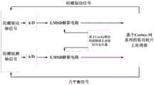
如图4所示,程序加载模块加载的程序包括相关的电路参数配置、陀螺驱动检测信号幅值和频率的PID闭环控制算法。电路参数配置包含LMSD解算模块和正余弦计算模块的参数设置。来自传感器的信号转化为数字量采集到系统后,经过LMSD解算模块进行处理,处理后的结果通过计算获得反馈信号用于对陀螺进行驱动和检测的力平衡闭环。其中,Cordic信号发生器用于产生LMSD解调所需的参考信号,以及产生驱动和力平衡信号的基准信号。As shown in Figure 4, the program loaded by the program loading module includes the relevant circuit parameter configuration, the PID closed-loop control algorithm of the amplitude and frequency of the gyro drive detection signal. The circuit parameter configuration includes the parameter settings of the LMSD calculation module and the sine-cosine calculation module. After the signal from the sensor is converted into a digital quantity and collected in the system, it is processed by the LMSD solving module, and the processed result is calculated to obtain a feedback signal for driving and detecting the force balance closed loop of the gyroscope. Among them, the Cordic signal generator is used to generate the reference signal required for LMSD demodulation, as well as the reference signal for driving and force balance signals.
在一个优选的实施例中,如图5所示,LMSD解算模块输出的信号解调结果包含同相分量和正交分量。待解调的信号(AD转化后的传感器信号)、参考正弦和余弦信号输入LMSD解算模块内。解调结果在系统复位时会被赋予初值,在解调过程中,解调结果组成的向量与参考信号组成的向量进行点积操作,并和待解调信号做减法,获得误差计算值。误差计算值乘上增益系数,并分别乘上两个参考信号,作为解调结果的增量值。解调结果与增量值做加法完成解调结果的更新。整个计算过程在电路中实现,每一次解调结果的更新花费1个时钟周期。In a preferred embodiment, as shown in FIG. 5 , the signal demodulation result output by the LMSD calculating module includes an in-phase component and a quadrature component. The signal to be demodulated (sensor signal after AD conversion), reference sine and cosine signals are input into the LMSD solving module. The demodulation result will be given an initial value when the system is reset. During the demodulation process, the vector composed of the demodulation result and the vector composed of the reference signal will be subjected to a dot product operation, and subtracted from the signal to be demodulated to obtain an error calculation value. The error calculation value is multiplied by the gain coefficient, and multiplied by the two reference signals respectively, as the incremental value of the demodulation result. The demodulation result is added to the incremental value to complete the update of the demodulation result. The entire calculation process is implemented in the circuit, and each update of the demodulation result takes 1 clock cycle.
优选的,LMSD解算模块是LMSD算法的数字电路实现。待解调信号U(k)为:Preferably, the LMSD calculation module is a digital circuit implementation of the LMSD algorithm. The signal U(k) to be demodulated is:
U(k)=a1sin(ωck)+a2·cos(ωck),U(k)=a1 sin(ωc k)+a2 cos(ωc k),
式中,a1、a2分别表示待解调信号在参考正弦信号、参考余弦信号上的幅值分量,ωc表示调制信号的调制频率,k表示采样个数,;sin(ωck)和cos(ωck)分别为参考正弦信号和参考余弦信号;In the formula, a1 and a2 represent the amplitude components of the signal to be demodulated on the reference sine signal and reference cosine signal respectively, ωc represents the modulation frequency of the modulation signal, k represents the number of samples, sin(ωc k) and cos(ωc k) are reference sine signal and reference cosine signal respectively;
按照下式计算参数矩阵W=(W1,W2)T:Calculate the parameter matrix W=(W1 ,W2 )T according to the following formula:
W(k+1)=W(k)+2·err(k)·μ·r(k).W(k+1)=W(k)+2·err(k)·μ·r(k).
其中μ是可变参数,r(k)=(sin(ωck),cos(ωck))T,err(k)=U(k)-WT·r(k)。Where μ is a variable parameter, r(k)=(sin(ωc k), cos(ωc k))T , err(k)=U(k)-WT ·r(k).
待解调信号在电路中先使用数字高通滤波器进行滤波处理,再进入LMSD解算模块进行信号解算。用于反馈的数字信号采用数字Sigma-Delta算法进行处理,处理电路采用四阶级联CIFF结构,对输出的正弦驱动信号进行调制,中心频率是电路参数,可以通过程序进行配置,调制位宽可变。The signal to be demodulated is first filtered by a digital high-pass filter in the circuit, and then enters the LMSD calculation module for signal calculation. The digital signal used for feedback is processed by a digital Sigma-Delta algorithm. The processing circuit adopts a four-stage cascaded CIFF structure to modulate the output sinusoidal drive signal. The center frequency is a circuit parameter, which can be configured through a program, and the modulation bit width is variable. .
在一个优选的实施例中,如图6所示,挂载在AHB总线上的正余弦计算模块采用查表插值的方式实现单个时钟周期完成正弦和余弦的计算。角度值使用32位定点整数量化,其中前11位用于进行查表,后21位参与到插值计算,最后将查表得到的结果和插值得到的结果通过算数运算,计算得到正弦值和余弦值。In a preferred embodiment, as shown in FIG. 6 , the sine and cosine calculation module mounted on the AHB bus uses a look-up table interpolation method to complete the calculation of sine and cosine in a single clock cycle. Angle values are quantized using 32-bit fixed-point integers. The first 11 bits are used for table lookup, and the last 21 bits are used for interpolation calculations. Finally, the results obtained from the table lookup and interpolation are calculated through arithmetic operations to obtain sine and cosine values. .
优选的,正余弦计算模块包含AHB总线上的单周期高速计算模块和APB总线上的低功耗计算模块。单周期高速计算模块采用查表插值法根据输入角度信号,计算正弦值和余弦值。输入角度为32位定点数,前11位用于查表,后32位用于线性插值。设前11位的数值为x,后21位的数值为y,那么对应的角度值为x+y,其正余弦计算公式为:Preferably, the sine-cosine calculation module includes a single-cycle high-speed calculation module on the AHB bus and a low-power calculation module on the APB bus. The single-cycle high-speed calculation module calculates the sine and cosine values according to the input angle signal by using the look-up table interpolation method. The input angle is a 32-bit fixed-point number, the first 11 bits are used for table lookup, and the last 32 bits are used for linear interpolation. Suppose the value of the first 11 digits is x, and the value of the last 21 digits is y, then the corresponding angle value is x+y, and its sine and cosine calculation formula is:
sin(x+y)=sin(x)+cos(x)·y,sin(x+y)=sin(x)+cos(x) y,
cos(x+y)=cos(x)-sin(x)·y.cos(x+y)=cos(x)-sin(x) y.
APB总线上的低功耗计算模块基于Cordic算法(已有的)实现,并使用28级流水线实现。The low-power computing module on the APB bus is implemented based on the Cordic algorithm (existing), and is implemented using a 28-stage pipeline.
综上,本发明提供的用于MEMS谐振式陀螺仪信号解调及控制的片上系统,其主要工作过程包含以下步骤:In summary, the system-on-chip for MEMS resonant gyroscope signal demodulation and control provided by the present invention, its main working process includes the following steps:
1)供电后从芯片引脚输入时钟信号;1) Input the clock signal from the chip pin after power supply;
2)选择程序加载方式;2) Select the program loading method;
3)在程序中设置陀螺信号的解调参数和控制算法;3) Set the demodulation parameters and control algorithm of the gyro signal in the program;
4)使用AD/DA驱动电路获得进行其他传感器的测控。4) Use the AD/DA drive circuit to obtain the measurement and control of other sensors.
上述步骤1)中,输入时钟的频率与芯片的系统时钟频率之间有如下关系:In the above step 1), there is the following relationship between the frequency of the input clock and the system clock frequency of the chip:

其中,fin是输入时钟的频率,fpll是芯片系统时钟频率,其他参数可以通过程序进行配置。Divpre表示预分频系数;Amp表示倍频系数;Divpost和Divmux是两个后分频系数;Among them,fin is the frequency of the input clock, fpll is the frequency of the chip system clock, and other parameters can be configured through the program. Divpre represents the prescaler coefficient; Amp represents the multiplier coefficient; Divpost and Divmux are two postscale coefficients;
上述步骤2)中,程序可以由片外FLASH、片上OTP或JTAG加载。默认使用片上OTP启动,可以通过配置启动引脚的高低电平修改成片外FLASH启动。当连接JTAG调试接口时默认使用JTAG进行程序加载。In the above step 2), the program can be loaded by off-chip FLASH, on-chip OTP or JTAG. By default, on-chip OTP is used to start, and it can be changed to off-chip FLASH by configuring the high and low levels of the start pin. When the JTAG debugging interface is connected, JTAG is used for program loading by default.
上述步骤3)中,通过SoC地址分配方式,对陀螺计算模块中相关参数进行赋值,并运行闭环控制算法。In the above step 3), the relevant parameters in the gyroscope computing module are assigned values through the SoC address allocation method, and the closed-loop control algorithm is run.
上述步骤4)中,通过AD/DA接口电路,对于使用AD7690 and DAC8812芯片的其他传感器,可以进行控制并获得测量结果以在CPU中进一步处理。In the above step 4), through the AD/DA interface circuit, other sensors using AD7690 and DAC8812 chips can be controlled and the measurement results can be obtained for further processing in the CPU.
上述各实施例仅用于说明本发明,各部件的结构、尺寸、设置位置及形状都是可以有所变化的,在本发明技术方案的基础上,凡根据本发明原理对个别部件进行的改进和等同变换,均不应排除在本发明的保护范围之外。The above-mentioned embodiments are only used to illustrate the present invention, and the structure, size, location and shape of each component can be changed. On the basis of the technical solution of the present invention, all improvements to individual components according to the principles of the present invention and equivalent transformations shall not be excluded from the protection scope of the present invention.
本领域内的技术人员应明白,本申请的实施例可提供为方法、系统、或计算机程序产品。因此,本申请可采用完全硬件实施例、完全软件实施例、或结合软件和硬件方面的实施例的形式。而且,本申请可采用在一个或多个其中包含有计算机可用程序代码的计算机可用存储介质(包括但不限于磁盘存储器、CD-ROM、光学存储器等)上实施的计算机程序产品的形式。Those skilled in the art should understand that the embodiments of the present application may be provided as methods, systems, or computer program products. Accordingly, the present application may take the form of an entirely hardware embodiment, an entirely software embodiment, or an embodiment combining software and hardware aspects. Furthermore, the present application may take the form of a computer program product embodied on one or more computer-usable storage media (including but not limited to disk storage, CD-ROM, optical storage, etc.) having computer-usable program code embodied therein.
本申请是参照根据本申请实施例的方法、设备(系统)、和计算机程序产品的流程图和/或方框图来描述的。应理解可由计算机程序指令实现流程图和/或方框图中的每一流程和/或方框、以及流程图和/或方框图中的流程和/或方框的结合。可提供这些计算机程序指令到通用计算机、专用计算机、嵌入式处理机或其他可编程数据处理设备的处理器以产生一个机器,使得通过计算机或其他可编程数据处理设备的处理器执行的指令产生用于实现在流程图一个流程或多个流程和/或方框图一个方框或多个方框中指定的功能的装置。The present application is described with reference to flowcharts and/or block diagrams of methods, apparatus (systems), and computer program products according to embodiments of the present application. It should be understood that each procedure and/or block in the flowchart and/or block diagram, and a combination of procedures and/or blocks in the flowchart and/or block diagram can be realized by computer program instructions. These computer program instructions may be provided to a general purpose computer, special purpose computer, embedded processor, or processor of other programmable data processing equipment to produce a machine such that the instructions executed by the processor of the computer or other programmable data processing equipment produce a An apparatus for realizing the functions specified in one or more procedures of the flowchart and/or one or more blocks of the block diagram.
这些计算机程序指令也可存储在能引导计算机或其他可编程数据处理设备以特定方式工作的计算机可读存储器中,使得存储在该计算机可读存储器中的指令产生包括指令装置的制造品,该指令装置实现在流程图一个流程或多个流程和/或方框图一个方框或多个方框中指定的功能。These computer program instructions may also be stored in a computer-readable memory capable of directing a computer or other programmable data processing apparatus to operate in a specific manner, such that the instructions stored in the computer-readable memory produce an article of manufacture comprising instruction means, the instructions The device realizes the function specified in one or more procedures of the flowchart and/or one or more blocks of the block diagram.
这些计算机程序指令也可装载到计算机或其他可编程数据处理设备上,使得在计算机或其他可编程设备上执行一系列操作步骤以产生计算机实现的处理,从而在计算机或其他可编程设备上执行的指令提供用于实现在流程图一个流程或多个流程和/或方框图一个方框或多个方框中指定的功能的步骤。These computer program instructions can also be loaded onto a computer or other programmable data processing device, causing a series of operational steps to be performed on the computer or other programmable device to produce a computer-implemented process, thereby The instructions provide steps for implementing the functions specified in the flow chart or blocks of the flowchart and/or the block or blocks of the block diagrams.
Claims (7)
Priority Applications (1)
| Application Number | Priority Date | Filing Date | Title |
|---|---|---|---|
| CN202110053102.XACN112880657B (en) | 2021-01-15 | 2021-01-15 | System-on-a-chip for signal demodulation and control of MEMS resonant gyroscope |
Applications Claiming Priority (1)
| Application Number | Priority Date | Filing Date | Title |
|---|---|---|---|
| CN202110053102.XACN112880657B (en) | 2021-01-15 | 2021-01-15 | System-on-a-chip for signal demodulation and control of MEMS resonant gyroscope |
Publications (2)
| Publication Number | Publication Date |
|---|---|
| CN112880657A CN112880657A (en) | 2021-06-01 |
| CN112880657Btrue CN112880657B (en) | 2023-02-07 |
Family
ID=76047928
Family Applications (1)
| Application Number | Title | Priority Date | Filing Date |
|---|---|---|---|
| CN202110053102.XAActiveCN112880657B (en) | 2021-01-15 | 2021-01-15 | System-on-a-chip for signal demodulation and control of MEMS resonant gyroscope |
Country Status (1)
| Country | Link |
|---|---|
| CN (1) | CN112880657B (en) |
Families Citing this family (1)
| Publication number | Priority date | Publication date | Assignee | Title |
|---|---|---|---|---|
| CN119030547B (en)* | 2024-10-25 | 2025-02-18 | 华芯拓远(天津)科技有限公司 | Gyroscope interface system and method with quadrature error compensation and modal matching |
Citations (4)
| Publication number | Priority date | Publication date | Assignee | Title |
|---|---|---|---|---|
| CN201311294Y (en)* | 2008-11-28 | 2009-09-16 | 赵剑青 | MEMS gyroscope with programmable slice system |
| CN104061931A (en)* | 2014-05-21 | 2014-09-24 | 中国民航大学 | FPGA-based miniature portable multi-sensor attitude detection system |
| CN105486296A (en)* | 2015-10-30 | 2016-04-13 | 北京自动化控制设备研究所 | Dynamically-tuned-gyro digital rebalance loop based on FPGA (Field-Programmable Gate Array) |
| CN210005012U (en)* | 2019-05-31 | 2020-01-31 | 东南大学 | multi-loop digital closed-loop control device for silicon MEMS gyroscope |
Family Cites Families (4)
| Publication number | Priority date | Publication date | Assignee | Title |
|---|---|---|---|---|
| CN1225713C (en)* | 2003-01-15 | 2005-11-02 | 西安交通大学 | Chips for Smart Appliances |
| US8250921B2 (en)* | 2007-07-06 | 2012-08-28 | Invensense, Inc. | Integrated motion processing unit (MPU) with MEMS inertial sensing and embedded digital electronics |
| US8578775B2 (en)* | 2010-02-08 | 2013-11-12 | Freescale Semiconductor, Inc. | Generation, injection and use of pilot tones for gyro system characterization |
| US20140278205A1 (en)* | 2013-03-12 | 2014-09-18 | Invensense, Inc. | Embedded processor on an integrated mems sensor chip autonomously managing external sensor |
- 2021
- 2021-01-15CNCN202110053102.XApatent/CN112880657B/enactiveActive
Patent Citations (4)
| Publication number | Priority date | Publication date | Assignee | Title |
|---|---|---|---|---|
| CN201311294Y (en)* | 2008-11-28 | 2009-09-16 | 赵剑青 | MEMS gyroscope with programmable slice system |
| CN104061931A (en)* | 2014-05-21 | 2014-09-24 | 中国民航大学 | FPGA-based miniature portable multi-sensor attitude detection system |
| CN105486296A (en)* | 2015-10-30 | 2016-04-13 | 北京自动化控制设备研究所 | Dynamically-tuned-gyro digital rebalance loop based on FPGA (Field-Programmable Gate Array) |
| CN210005012U (en)* | 2019-05-31 | 2020-01-31 | 东南大学 | multi-loop digital closed-loop control device for silicon MEMS gyroscope |
Non-Patent Citations (4)
| Title |
|---|
| Design of SoC for Special Measurement and Control of MEMS Gyroscope Based on ARM Cortex-M3;Li Yang等;《2019 IEEE International Conference on Power, Intelligent Computing and Systems (ICPICS)》;20191231;296-298* |
| Li Yang等.Design of SoC for Special Measurement and Control of MEMS Gyroscope Based on ARM Cortex-M3.《2019 IEEE International Conference on Power, Intelligent Computing and Systems (ICPICS)》.2019,* |
| 基于AT89S52的MEMS陀螺信号采集与处理系统设计;阚如文等;《微型机与应用》(第14期);全文* |
| 微机械陀螺数字读出系统及其解调算法;周斌等;《清华大学学报(自然科学版)》;20041231;第44卷(第5期);637-640,644* |
Also Published As
| Publication number | Publication date |
|---|---|
| CN112880657A (en) | 2021-06-01 |
Similar Documents
| Publication | Publication Date | Title |
|---|---|---|
| CN202304840U (en) | Flexible gyroscope rebalancing loop board | |
| CN112880657B (en) | System-on-a-chip for signal demodulation and control of MEMS resonant gyroscope | |
| CN106482747A (en) | A kind of zero bias temperature compensation method of high accuracy gyroscope instrument | |
| CN116448142A (en) | Hemispherical resonator gyro balance mode calibration method | |
| CN115127534A (en) | Quartz gyroscope sine wave phase detection compensation method based on carrier modulation | |
| CN116592912A (en) | A real-time identification method of MEMS gyroscope coupling error coefficient based on quadrature demodulation | |
| JP6586735B2 (en) | Circuit device, physical quantity detection device, electronic device, and moving object | |
| CN116412837A (en) | Method for generating hemispherical resonance gyro force balance mode calibration electric signal | |
| EP1058390B1 (en) | R/D converter | |
| CN117490729B (en) | Orthogonal drift error detection method of hemispherical resonator gyroscope | |
| CN103743400A (en) | Magnetic heading resolver | |
| CN105910596B (en) | Circuit device, physical quantity detection device, electronic equipment, and moving body | |
| Grayver et al. | Automatic gain control ASIC for MEMS gyro applications | |
| CN109724579A (en) | A kind of gyrocompass scaling method, calculates equipment and storage medium at device | |
| Pokydko et al. | MEMS Gyroscope Based on MPU-6050 Sensor and ATmega328 Microcontroller | |
| CN115328266A (en) | Digitally controlled oscillator, signal generation method and electronic device | |
| CN114264318A (en) | Method and device for testing natural frequency of closed-loop fiber optic gyroscope | |
| CN116481563B (en) | A rate-integrating gyroscope measurement and control method and device based on virtual rotation of detection axis | |
| JP2019184608A (en) | Rotation angle detection device, rotation angle detection method and program | |
| CN119197508B (en) | A gyro accelerometer output system based on photoelectric encoder | |
| CN118092873B (en) | Three-self inertial navigation software architecture design method based on multi-core processor | |
| CN108645395B (en) | Three-floating gyroscope digital demodulation system and demodulation method | |
| CN115406466A (en) | A Prism Calibration Method for Inertial Orientation Equipment | |
| CN108955628B (en) | Navigation attitude research system for teaching | |
| Iozzi et al. | Fast prototyping flow for sensor interfaces |
Legal Events
| Date | Code | Title | Description |
|---|---|---|---|
| PB01 | Publication | ||
| PB01 | Publication | ||
| SE01 | Entry into force of request for substantive examination | ||
| SE01 | Entry into force of request for substantive examination | ||
| GR01 | Patent grant | ||
| GR01 | Patent grant |