CN112840593B - Clock domain crossing processing circuit - Google Patents
Clock domain crossing processing circuitDownload PDFInfo
- Publication number
- CN112840593B CN112840593BCN201880098604.0ACN201880098604ACN112840593BCN 112840593 BCN112840593 BCN 112840593BCN 201880098604 ACN201880098604 ACN 201880098604ACN 112840593 BCN112840593 BCN 112840593B
- Authority
- CN
- China
- Prior art keywords
- clock
- data
- input data
- frequency
- circuit
- Prior art date
- Legal status (The legal status is an assumption and is not a legal conclusion. Google has not performed a legal analysis and makes no representation as to the accuracy of the status listed.)
- Active
Links
Images


Classifications
- H—ELECTRICITY
- H04—ELECTRIC COMMUNICATION TECHNIQUE
- H04L—TRANSMISSION OF DIGITAL INFORMATION, e.g. TELEGRAPHIC COMMUNICATION
- H04L7/00—Arrangements for synchronising receiver with transmitter
- H04L7/0016—Arrangements for synchronising receiver with transmitter correction of synchronization errors
- H04L7/005—Correction by an elastic buffer
- H—ELECTRICITY
- H03—ELECTRONIC CIRCUITRY
- H03L—AUTOMATIC CONTROL, STARTING, SYNCHRONISATION OR STABILISATION OF GENERATORS OF ELECTRONIC OSCILLATIONS OR PULSES
- H03L7/00—Automatic control of frequency or phase; Synchronisation
- H03L7/06—Automatic control of frequency or phase; Synchronisation using a reference signal applied to a frequency- or phase-locked loop
- H03L7/08—Details of the phase-locked loop
- H03L7/081—Details of the phase-locked loop provided with an additional controlled phase shifter
- H03L7/0812—Details of the phase-locked loop provided with an additional controlled phase shifter and where no voltage or current controlled oscillator is used
- H03L7/0814—Details of the phase-locked loop provided with an additional controlled phase shifter and where no voltage or current controlled oscillator is used the phase shifting device being digitally controlled
- G—PHYSICS
- G06—COMPUTING OR CALCULATING; COUNTING
- G06F—ELECTRIC DIGITAL DATA PROCESSING
- G06F5/00—Methods or arrangements for data conversion without changing the order or content of the data handled
- G06F5/06—Methods or arrangements for data conversion without changing the order or content of the data handled for changing the speed of data flow, i.e. speed regularising or timing, e.g. delay lines, FIFO buffers; over- or underrun control therefor
- H—ELECTRICITY
- H03—ELECTRONIC CIRCUITRY
- H03L—AUTOMATIC CONTROL, STARTING, SYNCHRONISATION OR STABILISATION OF GENERATORS OF ELECTRONIC OSCILLATIONS OR PULSES
- H03L7/00—Automatic control of frequency or phase; Synchronisation
- H03L7/06—Automatic control of frequency or phase; Synchronisation using a reference signal applied to a frequency- or phase-locked loop
- H03L7/08—Details of the phase-locked loop
- H03L7/0807—Details of the phase-locked loop concerning mainly a recovery circuit for the reference signal
- H—ELECTRICITY
- H03—ELECTRONIC CIRCUITRY
- H03L—AUTOMATIC CONTROL, STARTING, SYNCHRONISATION OR STABILISATION OF GENERATORS OF ELECTRONIC OSCILLATIONS OR PULSES
- H03L7/00—Automatic control of frequency or phase; Synchronisation
- H03L7/06—Automatic control of frequency or phase; Synchronisation using a reference signal applied to a frequency- or phase-locked loop
- H03L7/08—Details of the phase-locked loop
- H03L7/081—Details of the phase-locked loop provided with an additional controlled phase shifter
- H03L7/0812—Details of the phase-locked loop provided with an additional controlled phase shifter and where no voltage or current controlled oscillator is used
- H03L7/0816—Details of the phase-locked loop provided with an additional controlled phase shifter and where no voltage or current controlled oscillator is used the controlled phase shifter and the frequency- or phase-detection arrangement being connected to a common input
- H—ELECTRICITY
- H03—ELECTRONIC CIRCUITRY
- H03L—AUTOMATIC CONTROL, STARTING, SYNCHRONISATION OR STABILISATION OF GENERATORS OF ELECTRONIC OSCILLATIONS OR PULSES
- H03L7/00—Automatic control of frequency or phase; Synchronisation
- H03L7/06—Automatic control of frequency or phase; Synchronisation using a reference signal applied to a frequency- or phase-locked loop
- H03L7/16—Indirect frequency synthesis, i.e. generating a desired one of a number of predetermined frequencies using a frequency- or phase-locked loop
- H03L7/18—Indirect frequency synthesis, i.e. generating a desired one of a number of predetermined frequencies using a frequency- or phase-locked loop using a frequency divider or counter in the loop
- H03L7/1806—Indirect frequency synthesis, i.e. generating a desired one of a number of predetermined frequencies using a frequency- or phase-locked loop using a frequency divider or counter in the loop the frequency divider comprising a phase accumulator generating the frequency divided signal
- H—ELECTRICITY
- H03—ELECTRONIC CIRCUITRY
- H03L—AUTOMATIC CONTROL, STARTING, SYNCHRONISATION OR STABILISATION OF GENERATORS OF ELECTRONIC OSCILLATIONS OR PULSES
- H03L7/00—Automatic control of frequency or phase; Synchronisation
- H03L7/24—Automatic control of frequency or phase; Synchronisation using a reference signal directly applied to the generator
Landscapes
- Engineering & Computer Science (AREA)
- Theoretical Computer Science (AREA)
- Computer Networks & Wireless Communication (AREA)
- Signal Processing (AREA)
- Physics & Mathematics (AREA)
- General Engineering & Computer Science (AREA)
- General Physics & Mathematics (AREA)
- Synchronisation In Digital Transmission Systems (AREA)
Abstract
Translated fromChinese
Description
Translated fromChinese技术领域technical field
本申请涉及电路技术领域,尤其涉及跨时钟域的处理电路。The present application relates to the field of circuit technology, and in particular, to a processing circuit that spans clock domains.
背景技术Background technique
Serdes(SERializer/DESerializer,串行器/解串器)作为一种重要的高速串行链路物理层技术,被广泛应用于各种通用I/O(Input and Output,输入输出)接口中,例如PCIe(Peripheral Component Interface Express,外设总线接口)、以太网(Ethernet)、以及SATA(Serial Advanced Technology Attachment,串行高级技术附件)等接口。在两个设备进行通信时,Serdes用于在数据发送端将多路低速并行数据信号转换成高速串行数据信号,经过传输介质后在接收端将高速串行数据信号重新转换成多路低速并行数据信号。随着高速串行链路技术的发展,Serdes的速率越来越高,而高速链路互联介质中的介质插入损耗(Insertion Loss,IL)也随之增大,因此在链路中需要引入重定时器(retimer)将信号的驱动能力放大,从而使得高速链路能够容忍更大的插入损耗。重定时器用于对高速串行链路上传输的数据信号进行中继,例如通过内部的时钟重构信号,使数据信号的传输能量增加。此外,重定时器也可以用于滤除链路抖动。从而降低数据传输的性能。Serdes (SERializer/DESerializer, serializer/deserializer), as an important high-speed serial link physical layer technology, is widely used in various general-purpose I/O (Input and Output, input and output) interfaces, such as Interfaces such as PCIe (Peripheral Component Interface Express, peripheral bus interface), Ethernet (Ethernet), and SATA (Serial Advanced Technology Attachment, Serial Advanced Technology Attachment). When two devices communicate, Serdes is used to convert multi-channel low-speed parallel data signals into high-speed serial data signals at the data sending end, and re-convert the high-speed serial data signals into multi-channel low-speed parallel data signals at the receiving end after passing through the transmission medium. data signal. With the development of high-speed serial link technology, the rate of Serdes is getting higher and higher, and the medium insertion loss (Insertion Loss, IL) in the high-speed link interconnection medium also increases, so it is necessary to introduce heavy weights in the link. The timer (retimer) amplifies the driving ability of the signal, so that the high-speed link can tolerate greater insertion loss. The retimer is used to relay the data signal transmitted on the high-speed serial link, for example, through the internal clock reconstruction signal to increase the transmission energy of the data signal. In addition, retimers can also be used to filter out link jitter. Thereby reducing the performance of data transmission.
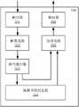
如图1所示的是现有技术中的一种重定时器(Retimer)100。由于高速串行链路中的信号衰减较大、链路中的高频抖动较多,重定时器100通常设置于高速串行链路中,以用作中继数据信号,以及滤除链路抖动。重定时器100包括接收端110、数据处理电路120以及发送端130。接收端110用于根据接收到的串行数据恢复出与串行数据对应的接收时钟信号,以及将串行数据转换为并行数据,并将并行数据和接收时钟信号输出至上述数据处理电路120。该数据处理电路120包括跨时钟域处理电路,该跨时钟域处理电路根据上述接收时钟信号,以及发送端130产生的发送时钟信号,通过一个弹性缓冲器(elastic buffer)对上述并行数据进行缓冲,并将缓冲后的并行数据输出至发送端130。此外,数据处理电路120还用于对上述并行数据进行编码、解码、加扰和解扰等处理。发送端130用于将数据处理电路120输出的上述并行数据转换为串行数据并输出。上述弹性缓冲器为一种数据缓存量可变的缓冲器,其数据缓存量由上述接收时钟信号和发送时钟信号确定。As shown in FIG. 1 is a retimer (Retimer) 100 in the prior art. Since the signal attenuation in the high-speed serial link is relatively large and the high-frequency jitter in the link is relatively high, the
上述接收时钟信号是根据接收的串行数据恢复出的时钟,而发送时钟信号是发送端130产生的时钟信号,即根据重定时器100的参考时钟产生的时钟信号,所以上述接收时钟信号和发送时钟信号会存在频率差,且该频率差是不固定的。因此,一方面数据处理电路120中的跨时钟域处理电路需要对并行数据进行异步时钟域的处理,使得并行数据从接收时钟信号的时钟域同步至发送时钟信号的时钟域,同时也要处理接收时钟信号和发送时钟信号之间存在的频偏(frequency skew,频率偏移)。在重定时器100中,现有技术的跨时钟域处理电路由于有上述弹性缓冲器的存在,导致数据处理延时非常大,使得数据经过重定时器的时间变长,从而降低了整个系统的数据处理性能。在某些传输协议下,当需要支持时钟扩频功能时,跨时钟域处理电路在对信号进行跨时钟域处理时会引入更大的延时,从而进一步降低了整个系统的数据处理性能,对于延时较为敏感的高速串行链路的影响尤为明显。The above-mentioned receiving clock signal is a clock recovered from the received serial data, and the transmitting clock signal is a clock signal generated by the transmitting
发明内容SUMMARY OF THE INVENTION
本申请的实施例提供一种跨时钟域处理电路,可以用于解决在数据在跨时钟域处理时延时较高的问题。Embodiments of the present application provide a cross-clock domain processing circuit, which can be used to solve the problem of high delay when data is processed across clock domains.
第一方面,本申请实施例提供一种跨时钟域处理电路,用于对输入数据进行跨时钟域处理。该跨时钟域处理电路包括滤抖电路和同步电路,其中滤抖电路用于对接收的输入数据时钟进行滤抖和相位调整,并作为输出数据时钟输出至同步电路。经过相位调整的输出数据时钟与上述输入数据时钟的相位对齐,其中上述输入数据时钟为根据输入数据恢复出的时钟,例如通过时钟恢复电路从输入数据中恢复出上述输入数据时钟。上述同步电路用于根据上述输入数据时钟和输出数据时钟,对输入数据进行跨时钟域的同步,以产生同步数据,即,将处于输入数据时钟的时钟域的输入数据同步至输出数据时钟的时钟域。In a first aspect, an embodiment of the present application provides a cross-clock-domain processing circuit for performing cross-clock-domain processing on input data. The cross-clock domain processing circuit includes a filter circuit and a synchronization circuit, wherein the filter circuit is used to filter and phase adjust the received input data clock, and output it to the synchronization circuit as an output data clock. The phase-adjusted output data clock is phase-aligned with the input data clock, wherein the input data clock is a clock recovered from the input data, for example, the input data clock is recovered from the input data by a clock recovery circuit. The above-mentioned synchronization circuit is used to synchronize the input data across the clock domain according to the above-mentioned input data clock and the output data clock to generate synchronous data, that is, to synchronize the input data in the clock domain of the input data clock to the clock of the output data clock. area.
由于跨时钟域处理电路将上述输入数据恢复出的时钟信号进行滤抖和相位调整,跨时钟域处理电路实质上无需额外的同步时钟,只需要利用恢复出的时钟信号即可实现输入数据的跨时钟域同步,因此节省了弹性缓冲器所占用的硬件资源,使得数据通过跨时钟域处理电路的时间更短,从而降低了跨时钟域处理电路处理数据的延时,提高了数据传输的效率。Since the clock signal recovered from the above input data is filtered and phase adjusted by the cross-clock domain processing circuit, the cross-clock domain processing circuit does not need an additional synchronous clock substantially, and only needs to use the recovered clock signal to realize the crossover of the input data. The clock domain is synchronized, so the hardware resources occupied by the elastic buffer are saved, and the time for data to pass through the cross-clock domain processing circuit is shorter, thereby reducing the delay of data processing by the cross-clock domain processing circuit and improving the efficiency of data transmission.
在一种可能的实施方式中,上述滤抖电路包括分频器、滤抖锁相环和相位插值器。其中,分频器用于对输入数据时钟进行分频,以得到频率较小的第一中间时钟;滤抖锁相环用于对上述第一中间时钟依次进行滤抖和倍频,以得到与输入数据时钟的频率相等的第二中间时钟;相位插值器用于调整第二中间时钟的相位,使得第二中间时钟的相位与输入数据时钟的相位对齐,且调整后的第二中间时钟即是上述输出数据时钟。通过对输入数据时钟进行上述处理,使得该时钟信号的抖动被滤除,并跟踪原输入数据时钟的相位,从而以较少的硬件资源产生用于同步的时钟。In a possible implementation, the above filter circuit includes a frequency divider, a filter phase locked loop and a phase interpolator. The frequency divider is used to divide the frequency of the input data clock to obtain a first intermediate clock with a smaller frequency; the filter phase-locked loop is used to sequentially filter and frequency multiply the above-mentioned first intermediate clock to obtain the same frequency as the input clock. The second intermediate clock with the same frequency of the data clock; the phase interpolator is used to adjust the phase of the second intermediate clock, so that the phase of the second intermediate clock is aligned with the phase of the input data clock, and the adjusted second intermediate clock is the above output data clock. By performing the above processing on the input data clock, the jitter of the clock signal is filtered out, and the phase of the original input data clock is tracked, thereby generating a clock for synchronization with less hardware resources.
在一种可能的实施方式中,上述相位插值器进一步用于:根据第二中间时钟产生第三中间时钟,且第二中间时钟与第三中间时钟的相位差为预设的相位差;对上述三个时钟信号进行鉴相,并确定相位关系;调整上述第二中间时钟和第三中间时钟的相位,使得输入数据时钟与第二中间时钟的相位差等于第三中间时钟与输入数据时钟的相位差,即第二中间时钟和第三中间时钟的上升沿关于输入数据时钟的上升沿对称。通过上述相位调整,使得第二中间时钟与输入数据时钟的相位对齐,从而能够用于同步上述输入数据。In a possible implementation manner, the above-mentioned phase interpolator is further configured to: generate a third intermediate clock according to the second intermediate clock, and the phase difference between the second intermediate clock and the third intermediate clock is a preset phase difference; Phase detection is performed on the three clock signals, and the phase relationship is determined; the phases of the second intermediate clock and the third intermediate clock are adjusted so that the phase difference between the input data clock and the second intermediate clock is equal to the phase between the third intermediate clock and the input data clock. The difference, that is, the rising edges of the second intermediate clock and the third intermediate clock are symmetrical with respect to the rising edge of the input data clock. Through the above-mentioned phase adjustment, the phases of the second intermediate clock and the input data clock are aligned, so as to be used for synchronizing the above-mentioned input data.
在一种可能的实施方式中,上述同步电路包括第一子同步电路和第二子同步电路,其中第一子同步电路用于根据输入数据时钟同步上述输入数据,并将结果输出至第二子同步电路;第二子同步电路根据第二中间时钟同步上述结果,得到上述同步数据。通过两个子同步电路来实现输入数据的同步处理,简化了跨时钟域处理电路的电路结构,节省了硬件面积和功耗。In a possible implementation manner, the synchronization circuit includes a first sub-synchronization circuit and a second sub-synchronization circuit, wherein the first sub-synchronization circuit is configured to synchronize the input data according to the input data clock, and output the result to the second sub-synchronization circuit A synchronization circuit; the second sub-synchronization circuit synchronizes the above result according to the second intermediate clock to obtain the above synchronization data. The synchronous processing of input data is realized by two sub-synchronization circuits, the circuit structure of the cross-clock domain processing circuit is simplified, and the hardware area and power consumption are saved.
在一种可能的实施方式中,上述第一子同步电路和第二子同步电路均为寄存器,且上述两个子同步电路分别通过输入数据时钟和第二中间时钟对输入数据进行同步。通过寄存器实现子同步电路,使得跨时钟域处理电路的电路复杂程度得到极大的简化,进一步节省硬件面积和功耗。In a possible implementation manner, the first sub-synchronization circuit and the second sub-synchronization circuit are both registers, and the two sub-synchronization circuits synchronize the input data through the input data clock and the second intermediate clock, respectively. The sub-synchronization circuit is realized by the register, so that the circuit complexity of the cross-clock domain processing circuit is greatly simplified, and the hardware area and power consumption are further saved.
在一种可能的实施方式中,上述滤抖锁相环包括鉴频鉴相器、环路滤波器、压控振荡器、反馈分频器和高速分频器,其中上述鉴频鉴相器用于接收上述第一中间时钟和反馈时钟,并对上述两个时钟信号进行鉴频鉴相,输出经过鉴频鉴相的比较结果;环路滤波器用于滤除上述比较结果中的抖动,并输出滤抖后的比较结果;压控振荡器用于根据上述滤抖后的比较结果产生频率大于第一中间时钟的第四中间时钟;反馈分频器将上述第四中间时钟分频至第一中间时钟的频率,并将分频后的结果反馈至鉴频鉴相器;高速分频器用于将上述第四中间时钟进行分频,并将分频后的第四中间时钟作为上述第二中间时钟。通过滤抖锁相环中的反馈回路结构,使得第一中间时钟中的抖动被滤除,从而提升同于同步的第二中间时钟的时钟质量。In a possible implementation manner, the above-mentioned filter phase-locked loop includes a frequency and phase detector, a loop filter, a voltage-controlled oscillator, a feedback frequency divider and a high-speed frequency divider, wherein the above-mentioned frequency and phase detector is used for Receive the above-mentioned first intermediate clock and the feedback clock, perform frequency and phase discrimination on the above-mentioned two clock signals, and output the comparison result after frequency and phase discrimination; the loop filter is used to filter out the jitter in the above-mentioned comparison result, and output the filter. The comparison result after shaking; the voltage-controlled oscillator is used to generate a fourth intermediate clock with a frequency greater than the first intermediate clock according to the comparison result after filtering; the feedback frequency divider divides the frequency of the fourth intermediate clock to the first intermediate clock The frequency of the frequency divider is fed back to the frequency and phase detector; the high-speed frequency divider is used to divide the frequency of the fourth intermediate clock, and use the divided fourth intermediate clock as the second intermediate clock. Through the feedback loop structure in the filter phase locked loop, the jitter in the first intermediate clock is filtered out, thereby improving the clock quality of the second intermediate clock that is synchronized.
在一种可能的实施方式中,上述滤抖锁相环还包括电荷泵,该电荷泵的输入端与鉴频鉴相器的输出端耦合,用于将鉴频鉴相器产生的频率和相位比较结果转换为稳定的模拟转换电压,并输出至压控振荡器。In a possible implementation, the above-mentioned filter phase-locked loop further includes a charge pump, the input end of the charge pump is coupled with the output end of the frequency discriminator and the phase discriminator, and is used for the frequency and phase generated by the frequency discriminator and phase discriminator. The comparison result is converted into a stable analog conversion voltage and output to the voltage-controlled oscillator.
在一种可能的实施方式中,上述跨时钟域处理电路还包括时钟恢复电路,该时钟恢复电路用于根据跨时钟域处理电路的工作时钟,恢复接收到的输入数据以得到输入数据时钟,并输出上述输入数据和输入数据时钟。通过时钟恢复电路对输入数据进行时钟恢复,使得恢复出的时钟可以经过滤抖等处理后再次用于同步输入数据,以实现跨时钟域的处理。In a possible implementation manner, the above-mentioned cross-clock domain processing circuit further includes a clock recovery circuit, the clock recovery circuit is configured to recover the received input data according to the operating clock of the cross-clock domain processing circuit to obtain the input data clock, and The above input data and input data clock are output. Clock recovery is performed on the input data through the clock recovery circuit, so that the recovered clock can be used to synchronize the input data again after processing such as filtering and shaking, so as to realize processing across clock domains.
在一种可能的实施方式中,上述输入数据为串行数据,且上述跨时钟域处理电路还包括串转并电路,该串转并电路用于将输入数据进行串并转换,并输出经过串并转换后的输入数据(即并行的输入数据)至上述同步电路和滤抖电路。相应的,同步电路中两个子同步电路之间的数据也为并行数据。当跨时钟域处理电路用于处理并行数据,可以提高数据同步的效率。In a possible implementation manner, the input data is serial data, and the cross-clock domain processing circuit further includes a serial-to-parallel circuit, the serial-to-parallel circuit is used to perform serial-to-parallel conversion on the input data, and output the serial-to-parallel conversion. And the converted input data (ie, the parallel input data) is sent to the above-mentioned synchronization circuit and filter circuit. Correspondingly, the data between the two sub-synchronization circuits in the synchronization circuit is also parallel data. When the cross-clock domain processing circuit is used to process parallel data, the efficiency of data synchronization can be improved.
在一种可能的实施方式中,上述滤抖电路进一步用于对上述输入数据时钟进行高频滤抖,其中输入数据时钟和输出数据时钟均包括扩频时钟SSC信息。相应的,滤抖锁相环中的环路滤波器进一步用于对鉴频鉴相器输出的比较结果进行高频滤抖。当滤抖电路对输入数据时钟进行高频滤抖时,时钟携带的低频抖动可以被保留,并伴随同步数据输出至下游的设备,使得跨时钟域电路可以支持传输链路中的特定协议或预设的功能,例如开启和关闭SRIS功能。In a possible implementation manner, the above-mentioned filtering circuit is further configured to perform high-frequency filtering on the above-mentioned input data clock, wherein both the input data clock and the output data clock include spread spectrum clock SSC information. Correspondingly, the loop filter in the filter phase-locked loop is further used to perform high-frequency filtering on the comparison result output by the frequency and phase detector. When the jittering circuit performs high-frequency filtering on the input data clock, the low-frequency jitter carried by the clock can be retained and output to downstream devices along with the synchronous data, so that the cross-clock domain circuit can support a specific protocol or preset in the transmission link. settings, such as turning the SRIS function on and off.
在一种可能的实施方式中,高频抖动包括抖动频率大于0.005f的抖动,其中f为时钟信号的频率。高频滤抖用于滤除上述高频抖动。当滤抖电路对输入数据时钟进行高频滤抖时,时钟携带的低频抖动可以被保留,并伴随同步数据输出至下游的设备,使得跨时钟域电路可以支持传输链路中的特定协议或预设的功能,例如开启和关闭SRIS功能。In a possible implementation, the high frequency jitter includes jitter with a jitter frequency greater than 0.005f, where f is the frequency of the clock signal. The high-frequency filter is used to filter out the above-mentioned high-frequency jitter. When the jittering circuit performs high-frequency filtering on the input data clock, the low-frequency jitter carried by the clock can be retained and output to downstream devices along with the synchronous data, so that the cross-clock domain circuit can support a specific protocol or preset in the transmission link. settings, such as turning the SRIS function on and off.
在一种可能的实施方式中,发送端发送输入数据至跨时钟域处理电路,且同步数据输出至接收端,其中存在以下三种情况:其一、上述发送端和跨时钟域处理电路共用一个参考时钟,接收端的工作时钟与上述共用的参考时钟独立;其二、上述接收端和跨时钟域处理电路共用一个参考时钟,发送端的参考时钟与上述共用的参考时钟独立;其三、上述发送端、接收端和跨时钟域处理电路共用一个参考时钟。其中,上述发送端和接收端可以是设备,也可以是电路或者电路包括的功能模块、单元,也可以是接口。跨时钟域处理电路的参考时钟可以独立于接收端和发送端,也可以共用参考时钟,使得其时钟信号的配置更加灵活。In a possible implementation, the sending end sends input data to the cross-clock domain processing circuit, and the synchronous data is output to the receiving end. There are the following three situations: First, the above-mentioned sending end and the cross-clock domain processing circuit share one Reference clock, the working clock of the receiving end is independent of the above-mentioned shared reference clock; secondly, the above-mentioned receiving end and the cross-clock domain processing circuit share a reference clock, and the reference clock of the transmitting end is independent of the above-mentioned shared reference clock; thirdly, the above-mentioned transmitting end , the receiver and the cross-clock domain processing circuit share a reference clock. Wherein, the above-mentioned sending end and receiving end may be devices, circuits or functional modules and units included in circuits, or interfaces. The reference clock of the cross-clock domain processing circuit can be independent of the receiving end and the transmitting end, or can share the reference clock, which makes the configuration of the clock signal more flexible.
第二方面,本申请实施例提供一种重定时器,用于对传输链路中的N路输入数据进行中继。该重定时器包括滤抖电路和N个同步电路(N≥1且N为正整数),其中滤抖电路用于对接收的输入数据时钟进行滤抖和相位调整,并作为输出数据时钟输出至同步电路。经过相位调整的输出数据时钟与上述输入数据时钟的相位对齐,其中上述输入数据时钟为时钟恢复电路根据N路输入数据恢复出的N个恢复数据时钟中的任意一个恢复数据时钟,例如通过时钟恢复电路从N路输入数据中恢复出N个恢复数据时钟,并选择其中一个恢复时钟作为上述输入数据时钟。每个同步电路用于根据上述输入数据时钟和输出数据时钟,对输入数据进行跨时钟域的同步,以产生一路同步数据,即,将处于输入数据时钟的时钟域的输入数据同步至输出数据时钟的时钟域。In a second aspect, an embodiment of the present application provides a retimer for relaying N channels of input data in a transmission link. The retimer includes a filter circuit and N synchronization circuits (N≥1 and N is a positive integer), wherein the filter circuit is used to filter and phase adjust the received input data clock, and output it as an output data clock to synchronization circuit. The phase-adjusted output data clock is aligned with the phase of the input data clock, wherein the input data clock is any one of the N recovered data clocks recovered by the clock recovery circuit according to the N channels of input data, for example, through clock recovery The circuit recovers N recovered data clocks from the N channels of input data, and selects one of the recovered clocks as the above input data clock. Each synchronization circuit is used for synchronizing the input data across the clock domain according to the above-mentioned input data clock and output data clock to generate one channel of synchronous data, that is, synchronizing the input data in the clock domain of the input data clock to the output data clock clock domain.
由于重定时器将上述N路输入数据恢复出的时钟信号进行滤抖和相位调整,跨时钟域处理电路实质上无需额外的同步时钟,只需要利用恢复出的时钟信号即可实现输入数据的跨时钟域同步,因此节省了弹性缓冲器所占用的硬件资源,使得数据通过重定时器的时间更短,从而降低了重定时器处理数据的延时,提高了数据传输的效率。Since the retimer filters and adjusts the phase of the clock signal recovered from the above N channels of input data, the cross-clock domain processing circuit does not need an additional synchronous clock in essence, and only the recovered clock signal can be used to realize the crossover of the input data. The clock domain is synchronized, so the hardware resources occupied by the elastic buffer are saved, and the time for data to pass through the retimer is shorter, thereby reducing the delay of data processing by the retimer and improving the efficiency of data transmission.
在一种可能的实施方式中,上述滤抖电路包括分频器、滤抖锁相环和相位插值器。其中,分频器用于对输入数据时钟进行分频,以得到频率较小的第一中间时钟;滤抖锁相环用于对上述第一中间时钟依次进行滤抖和倍频,以得到与输入数据时钟的频率相等的第二中间时钟;相位插值器用于调整第二中间时钟的相位,使得第二中间时钟的相位与输入数据时钟的相位对齐,且调整后的第二中间时钟即是上述输出数据时钟。通过对输入数据时钟进行上述处理,使得该时钟信号的抖动被滤除,并跟踪原输入数据时钟的相位,从而以较少的硬件资源产生用于同步的时钟。In a possible implementation, the above filter circuit includes a frequency divider, a filter phase locked loop and a phase interpolator. The frequency divider is used to divide the frequency of the input data clock to obtain a first intermediate clock with a smaller frequency; the filter phase-locked loop is used to sequentially filter and frequency multiply the above-mentioned first intermediate clock to obtain the same frequency as the input clock. The second intermediate clock with the same frequency of the data clock; the phase interpolator is used to adjust the phase of the second intermediate clock, so that the phase of the second intermediate clock is aligned with the phase of the input data clock, and the adjusted second intermediate clock is the above output data clock. By performing the above processing on the input data clock, the jitter of the clock signal is filtered out, and the phase of the original input data clock is tracked, thereby generating a clock for synchronization with less hardware resources.
在一种可能的实施方式中,上述相位插值器进一步用于:根据第二中间时钟产生第三中间时钟,且第二中间时钟与第三中间时钟的相位差为预设的相位差;对上述三个时钟信号进行鉴相,并确定相位关系;调整上述第二中间时钟和第三中间时钟的相位,使得输入数据时钟与第二中间时钟的相位差等于第三中间时钟与输入数据时钟的相位差,即第二中间时钟和第三中间时钟的上升沿关于输入数据时钟的上升沿对称。通过上述相位调整,使得第二中间时钟与输入数据时钟的相位对齐,从而能够用于同步上述输入数据。In a possible implementation manner, the above-mentioned phase interpolator is further configured to: generate a third intermediate clock according to the second intermediate clock, and the phase difference between the second intermediate clock and the third intermediate clock is a preset phase difference; Phase detection is performed on the three clock signals, and the phase relationship is determined; the phases of the second intermediate clock and the third intermediate clock are adjusted so that the phase difference between the input data clock and the second intermediate clock is equal to the phase between the third intermediate clock and the input data clock. The difference, that is, the rising edges of the second intermediate clock and the third intermediate clock are symmetrical with respect to the rising edge of the input data clock. Through the above-mentioned phase adjustment, the phases of the second intermediate clock and the input data clock are aligned, so as to be used for synchronizing the above-mentioned input data.
在一种可能的实施方式中,上述N个同步电路中的每个同步电路均包括一个第一子同步电路和一个第二子同步电路,其中第一子同步电路用于根据输入数据时钟同步上述N路输入数据中的一路,并将结果输出至第二子同步电路;第二子同步电路根据第二中间时钟同步上述结果,得到上述同步数据中的一路同步数据。通过两个子同步电路来实现输入数据的同步处理,简化了重定时器的电路结构,节省了硬件面积和功耗。In a possible implementation manner, each of the above-mentioned N synchronization circuits includes a first sub-synchronization circuit and a second sub-synchronization circuit, wherein the first sub-synchronization circuit is used for synchronizing the above-mentioned synchronization according to the input data clock One of the N channels of input data is output to the second sub-synchronization circuit; the second sub-synchronization circuit synchronizes the above result according to the second intermediate clock to obtain one channel of the above-mentioned synchronization data. The synchronous processing of input data is realized by two sub-synchronization circuits, the circuit structure of the retimer is simplified, and the hardware area and power consumption are saved.
在一种可能的实施方式中,上述第一子同步电路和第二子同步电路均为寄存器,且上述两个子同步电路分别通过输入数据时钟和第二中间时钟对输入数据进行同步。通过寄存器实现子同步电路,使得重定时器的电路复杂程度得到极大的简化,进一步节省硬件面积和功耗。In a possible implementation manner, the first sub-synchronization circuit and the second sub-synchronization circuit are both registers, and the two sub-synchronization circuits synchronize the input data through the input data clock and the second intermediate clock, respectively. The sub-synchronization circuit is realized by the register, which greatly simplifies the circuit complexity of the retimer and further saves the hardware area and power consumption.
在一种可能的实施方式中,上述滤抖锁相环包括鉴频鉴相器、环路滤波器、压控振荡器、反馈分频器和高速分频器,其中上述鉴频鉴相器用于接收上述第一中间时钟和反馈时钟,并对上述两个时钟信号进行鉴频鉴相,输出经过鉴频鉴相的比较结果;环路滤波器用于滤除上述比较结果中的抖动,并输出滤抖后的比较结果;压控振荡器用于根据上述滤抖后的比较结果产生频率大于第一中间时钟的第四中间时钟;反馈分频器将上述第四中间时钟分频至第一中间时钟的频率,并将分频后的结果反馈至鉴频鉴相器;高速分频器用于将上述第四中间时钟进行分频,并将分频后的第四中间时钟作为上述第二中间时钟。通过滤抖锁相环中的反馈回路结构,使得第一中间时钟中的抖动被滤除,从而提升同于同步的第二中间时钟的时钟质量。In a possible implementation manner, the above-mentioned filter phase-locked loop includes a frequency and phase detector, a loop filter, a voltage-controlled oscillator, a feedback frequency divider and a high-speed frequency divider, wherein the above-mentioned frequency and phase detector is used for Receive the above-mentioned first intermediate clock and the feedback clock, perform frequency and phase discrimination on the above-mentioned two clock signals, and output the comparison result after frequency and phase discrimination; the loop filter is used to filter out the jitter in the above-mentioned comparison result, and output the filter. The comparison result after shaking; the voltage-controlled oscillator is used to generate a fourth intermediate clock with a frequency greater than the first intermediate clock according to the comparison result after filtering; the feedback frequency divider divides the frequency of the fourth intermediate clock to the first intermediate clock The frequency of the frequency divider is fed back to the frequency and phase detector; the high-speed frequency divider is used to divide the frequency of the fourth intermediate clock, and use the divided fourth intermediate clock as the second intermediate clock. Through the feedback loop structure in the filter phase locked loop, the jitter in the first intermediate clock is filtered out, thereby improving the clock quality of the second intermediate clock that is synchronized.
在一种可能的实施方式中,上述滤抖锁相环还包括电荷泵,该电荷泵的输入端与鉴频鉴相器的输出端耦合,用于将鉴频鉴相器产生的频率和相位比较结果转换为稳定的模拟转换电压,并输出至压控振荡器。In a possible implementation, the above-mentioned filter phase-locked loop further includes a charge pump, the input end of the charge pump is coupled with the output end of the frequency discriminator and the phase discriminator, and is used for the frequency and phase generated by the frequency discriminator and phase discriminator. The comparison result is converted into a stable analog conversion voltage and output to the voltage-controlled oscillator.
在一种可能的实施方式中,上述重定时器还包括N个时钟恢复电路,用于分别根据重定时器的工作时钟,恢复接收到的输入数据以得到上述N路恢复数据时钟,并输出上述输入数据和N路恢复数据时钟。通过时钟恢复电路对输入数据进行时钟恢复,使得恢复出的时钟可以经过滤抖等处理后再次用于同步输入数据,以实现跨时钟域的处理。In a possible implementation manner, the retimer further includes N clock recovery circuits for recovering the received input data according to the working clocks of the retimer to obtain the N channels of recovered data clocks, and outputting the above Input data and N-way recovered data clock. Clock recovery is performed on the input data through the clock recovery circuit, so that the recovered clock can be used to synchronize the input data again after processing such as filtering and shaking, so as to realize processing across clock domains.
在一种可能的实施方式中,上述重定时器还包括N个串转并电路,且上述N路输入数据为N路串行数据,其中上述N个串转并电路用于分别对N路输入数据进行串并转换,并输出转后的结果(即N路并行数据)至上述N个同步电路和滤抖电路。通过对数据进行串行转并行的转换,可以将传输链路中的高速串行数据转换为并行数据,提高重定时器对数据处理的效率,节省数据处理时间。In a possible implementation manner, the retimer further includes N serial-to-parallel circuits, and the N channels of input data are N channels of serial data, wherein the N series-to-parallel circuits are used to respectively input the N channels of data. Serial-to-parallel conversion is performed on the data, and the converted result (ie, N channels of parallel data) is output to the above-mentioned N synchronization circuits and filter circuits. By converting the data from serial to parallel, the high-speed serial data in the transmission link can be converted into parallel data, which improves the efficiency of data processing by the retimer and saves data processing time.
在一种可能的实施方式中,上述重定时器还包括N个并转串电路,且上述N路同步数据为N路并行数据,其中上述N个并转串电路用于分别对N路同步数据进行并行转串行的转换,并输出转换后的结果。通过对数据进行并行转串的转换,可以将处理(同步)后的数据重新转换为高速的串行信号,提高重定时器对数据处理的效率,节省数据处理时间。In a possible implementation manner, the retimer further includes N parallel-to-serial circuits, and the N channels of synchronization data are N channels of parallel data, wherein the N parallel-to-serial circuits are used to convert the N channels of synchronization data respectively. Perform parallel-to-serial conversion and output the converted result. By performing parallel-to-serial conversion on the data, the processed (synchronized) data can be re-converted into high-speed serial signals, thereby improving the data processing efficiency of the retimer and saving data processing time.
在一种可能的实施方式中,上述重定时器还包括N个数据处理电路和N个数据选择器,其中N个数据处理电路的输入端分别与N个时钟恢复电路的输出端耦合,N个数据处理电路的输出端分别与N个数据选择器的输入端耦合,N个数据处理电路用于分别对接收的N路输入数据进行解码、解扰、同步、加扰和编码;对于每一个相互耦合的数据处理电路、时钟恢复电路和数据选择器,数据选择器的两个输入端分别与时钟恢复电路的输出端和数据处理电路的输出端耦合,而数据选择器的输出端与同步电路的输出端耦合。可以通过额外的控制信号来控制数据选择器,从而选择上述两个输入端中接收的两路数据信号的其中一路作为输出。在重定时器中,数据可以通过数据选择器直接进行跨时钟域的同步,也可以先进过数据处理电路的处理后,再通过数据选择器进行跨时钟域的同步,使得重定时器处理输入数据的方式更加灵活,可以根据不同的传输协议选择是否直通数据,从而提高中继数据的效率。In a possible implementation manner, the above-mentioned retimer further includes N data processing circuits and N data selectors, wherein the input terminals of the N data processing circuits are respectively coupled to the output terminals of the N clock recovery circuits, and the N The output terminals of the data processing circuit are respectively coupled with the input terminals of the N data selectors, and the N data processing circuits are used to decode, descramble, synchronize, scramble and encode the received N channels of input data; The coupled data processing circuit, the clock recovery circuit and the data selector, the two input terminals of the data selector are respectively coupled with the output terminal of the clock recovery circuit and the output terminal of the data processing circuit, and the output terminal of the data selector is connected with the output terminal of the synchronization circuit. output coupling. The data selector can be controlled by an additional control signal, so as to select one of the two data signals received in the above two input terminals as an output. In the retimer, the data can be directly synchronized across the clock domain through the data selector, or it can be processed by the data processing circuit first, and then synchronized across the clock domain through the data selector, so that the retimer can process the input data. The method is more flexible, and whether to pass through data can be selected according to different transmission protocols, thereby improving the efficiency of relaying data.
在一种可能的实施方式中,上述滤抖电路进一步用于对上述输入数据时钟进行高频滤抖,其中输入数据时钟和输出数据时钟均包括扩频时钟SSC信息。相应的,滤抖锁相环中的环路滤波器进一步用于对鉴频鉴相器输出的比较结果进行高频滤抖。当滤抖电路对输入数据时钟进行高频滤抖时,时钟携带的低频抖动可以被保留,并伴随同步数据输出至下游的设备,使得跨时钟域电路可以支持传输链路中的特定协议或预设的功能,例如开启和关闭SRIS功能。In a possible implementation manner, the above-mentioned filtering circuit is further configured to perform high-frequency filtering on the above-mentioned input data clock, wherein both the input data clock and the output data clock include spread spectrum clock SSC information. Correspondingly, the loop filter in the filter phase-locked loop is further used to perform high-frequency filtering on the comparison result output by the frequency and phase detector. When the jittering circuit performs high-frequency filtering on the input data clock, the low-frequency jitter carried by the clock can be retained and output to downstream devices along with the synchronous data, so that the cross-clock domain circuit can support a specific protocol or preset in the transmission link. settings, such as turning the SRIS function on and off.
在一种可能的实施方式中,高频抖动包括抖动频率大于0.005f的抖动,其中f为时钟信号的频率。高频滤抖用于滤除上述高频抖动。当滤抖电路对输入数据时钟进行高频滤抖时,时钟携带的低频抖动可以被保留,并伴随同步数据输出至下游的设备,使得跨时钟域电路可以支持传输链路中的特定协议或预设的功能,例如开启和关闭SRIS功能。In a possible implementation, the high frequency jitter includes jitter with a jitter frequency greater than 0.005f, where f is the frequency of the clock signal. The high-frequency filter is used to filter out the above-mentioned high-frequency jitter. When the jittering circuit performs high-frequency filtering on the input data clock, the low-frequency jitter carried by the clock can be retained and output to downstream devices along with the synchronous data, so that the cross-clock domain circuit can support a specific protocol or preset in the transmission link. settings, such as turning the SRIS function on and off.
在一种可能的实施方式中,发送端发送输入数据至跨时钟域处理电路,且同步数据输出至接收端,其中存在以下三种情况:其一、上述发送端和跨时钟域处理电路共用一个参考时钟,接收端的工作时钟与上述共用的参考时钟独立;其二、上述接收端和跨时钟域处理电路共用一个参考时钟,发送端的参考时钟与上述共用的参考时钟独立;其三、上述发送端、接收端和跨时钟域处理电路共用一个参考时钟。其中,上述发送端和接收端可以是设备,也可以是电路或者电路包括的功能模块、单元,也可以是接口。跨时钟域处理电路的参考时钟可以独立于接收端和发送端,也可以共用参考时钟,使得其时钟信号的配置更加灵活。In a possible implementation, the sending end sends input data to the cross-clock domain processing circuit, and the synchronous data is output to the receiving end. There are the following three situations: First, the above-mentioned sending end and the cross-clock domain processing circuit share one Reference clock, the working clock of the receiving end is independent of the above-mentioned shared reference clock; secondly, the above-mentioned receiving end and the cross-clock domain processing circuit share a reference clock, and the reference clock of the transmitting end is independent of the above-mentioned shared reference clock; thirdly, the above-mentioned transmitting end , the receiver and the cross-clock domain processing circuit share a reference clock. Wherein, the above-mentioned sending end and receiving end may be devices, circuits or functional modules and units included in circuits, or interfaces. The reference clock of the cross-clock domain processing circuit can be independent of the receiving end and the transmitting end, or can share the reference clock, which makes the configuration of the clock signal more flexible.
在一种可能的实施方式中,上述重定时器为多通道的重定时器,其中N≥2,且N为正整数。通过增加重定时器中同步电路、时钟恢复电路等电路的数量,使得重定时器可以同时对多路输入数据进行处理,从而进一步提高重定时器中继数据的效率。In a possible implementation manner, the above-mentioned retimer is a multi-channel retimer, wherein N≧2, and N is a positive integer. By increasing the number of synchronizing circuits, clock recovery circuits and other circuits in the retimer, the retimer can process multiple input data at the same time, thereby further improving the efficiency of the retimer relaying data.
附图说明Description of drawings
为了更清楚地说明本申请实施例或现有技术中的技术方案,下面将对实施例或现有技术描述中所需要使用的附图作简单地介绍。In order to more clearly illustrate the embodiments of the present application or the technical solutions in the prior art, the following briefly introduces the accompanying drawings that are required to be used in the description of the embodiments or the prior art.
图1为现有技术中的一种重定时器。FIG. 1 is a retimer in the prior art.
图2为本申请实施例中一种重定时器。FIG. 2 is a retimer in an embodiment of the present application.
图3为本申请实施例中一种具体的重定时器。FIG. 3 is a specific retimer in an embodiment of the present application.
图4为本申请实施例中一种滤抖电路。FIG. 4 is a filter circuit in an embodiment of the present application.
图5为本申请实施例中相位插值器的时序图。FIG. 5 is a timing diagram of a phase interpolator in an embodiment of the present application.
图6为本申请实施例中一种滤抖锁相环。FIG. 6 is a filter phase-locked loop in an embodiment of the present application.
图7为本申请实施例中一种同步电路。FIG. 7 is a synchronization circuit in an embodiment of the present application.
图8为本申请实施例中一种更为具体的重定时器。FIG. 8 is a more specific retimer in an embodiment of the present application.
图9为本申请实施例中一种数据处理电路。FIG. 9 is a data processing circuit in an embodiment of the present application.
图10为本申请实施例中一种多通道重定时器。FIG. 10 is a multi-channel retimer in an embodiment of the present application.
附图标记:重定时器300;数据接收电路310;时钟恢复电路312;串转并电路314;均衡器316;第一时钟电路318;数据发送电路320;滤抖电路330;同步电路340;数据处理电路350;数据选择器360;并转串电路370。Reference numerals:
具体实施方式Detailed ways
下面将结合本申请实施例中的附图,对本申请实施例中的技术方案进行清楚、完整地描述。The technical solutions in the embodiments of the present application will be clearly and completely described below with reference to the accompanying drawings in the embodiments of the present application.
为解决重定时器延时较大的问题,本申请实施例提供如图2所示的一种重定时器300。该重定时器300设置于第一设备210和第二设备220之间的高速串行通信链路上。该通信链路可以为采用PCIe(Peripheral Component Interface Express,外设总线接口)、以太网(Ethernet)、以及SATA(Serial Advanced Technology Attachment,串行高级技术附件)、SAS(Serial Attached SCSI,串行连接SCSI接口)、USB(Universal Serial Bus,通用串行总线)等协议的通信链路。重定时器300用于中继数据信号,例如通过内部的时钟重构信号,使数据信号的传输能量增加。重定时器300还可以用于滤除上述通信链路中的抖动。上述数据信号可以是从第一设备210发送给第二设备220的数据信号,也可以是第二设备220发送给第一设备210的数据信号。上述第一设备和第二设备可以包括终端设备,例如手机、平板电脑;也可以包括服务器设备,或通信基站;或者包括设置于两个独立的PCB(Printed Circuit Board,印制电路板)上的电路。To solve the problem that the retimer has a relatively large delay, an embodiment of the present application provides a
如图3所示的是重定时器300的一种具体的实施方式。重定时器300包括接收电路310和发送电路320,其中接收电路310包括时钟恢复电路312和串转并电路314,该时钟恢复电路312用于根据接收电路310的工作时钟将接收的串行数据进行时钟恢复,以得到输入数据时钟,同时输出上述串行数据,以及恢复出的输入数据时钟;上述串转并电路314用于将该串行数据转换为并行数据并输出该并行数据。其中接收电路310的工作时钟可以根据重定时器300的参考时钟确定。时钟恢复电路312可以通过检测串行数据的相位来实现时钟的恢复,时钟恢复电路312有多种实现方式,例如使用无源滤波器和限幅放大器实现,使用窄频再生分频器,使用同步振荡器实现,或者使用锁相环等。A specific implementation of the
发送电路320用于对接收电路310输出的并行数据进行跨时钟域同步,并将同步后的并行数据转换为串行数据输出至第二设备220。具体来说,发送电路320包括滤抖电路330、同步电路340和并转串电路370。滤抖电路330用于接收时钟恢复电路312输出的输入数据时钟,将该输入数据时钟进行滤抖,调整滤抖后的输入数据时钟的相位,并产生输出数据时钟,使得该输出数据时钟的相位与输入数据时钟的相位对齐。在一种实施方式中,滤抖电路330对上述输入数据时钟的滤抖可以为高频滤抖,此时输入数据时钟经过滤抖电路330后,其高频分量的抖动被滤除,同时低频分量的抖动被保留,且上述低频分量可以携带有用的时钟信息。同步电路340用于根据上述输入数据时钟,以及上述输出数据时钟,对时钟恢复电路312产生的上述并行数据进行跨时钟域的同步,并产生同步数据,其中该同步数据处于输出数据时钟的时钟域。由于接收电路310中的数据处于输入数据时钟的时钟域,而发送电路320中的数据处于输出数据时钟的时钟域,因此同步电路340将上述并行数据从输入数据时钟的时钟域同步至输出数据时钟的时钟域。并转串电路370用于将接收的上述同步数据转换为串行输出数据,并输出该串行输出数据至第二设备220。上述高频分量的抖动包括高速串行通信链路产生的高频抖动,以及时钟恢复电路312在恢复时钟时产生的高频抖动。The sending
需要注意的是,本申请中高频抖动和高频滤抖中的“高频”应为本领域技术人员熟知的概念。例如,对于频率为f的时钟信号,其携带的频率大于0.005f的抖动都应该认为是高频抖动。相应的,高频滤抖为滤除频率大于0.005f的抖动。更为具体的,本申请实施例提供的滤抖电路330可以对100MHz的时钟信号进行高频滤抖,则该时钟信号携带的频率高于500KHz的抖动均会被滤除。相应的,低频抖动为频率小于0.005f的抖动。此外,本申请中的相位对齐可以理解为,两个时钟信号的上升沿的相位差为一个固定值,例如相位差保持-30°、保持0°或者保持30°。It should be noted that "high frequency" in high frequency dithering and high frequency filtering in this application should be a concept well known to those skilled in the art. For example, for a clock signal with a frequency of f, the jitter with a frequency greater than 0.005f should be considered as high-frequency jitter. Correspondingly, the high-frequency filter is to filter out the jitter whose frequency is greater than 0.005f. More specifically, the
由于重定时器300将上述输入数据恢复出的时钟信号进行滤抖和相位调整,并将该时钟信号用于输入数据的跨时钟域同步,重定时器300在中继数据时无需通过弹性缓冲器来同步时钟域,使得数据通过重定时器300的时间更短,从而降低了重定时器300处理数据的延时,尤其是数据在跨时钟域时的延迟,提高了数据传输的效率。Since the
如图4所示的是上述滤抖电路330的一种具体的实施方式。滤抖电路330包括分频器(Divider,DIV)332、滤抖锁相环334和相位插值器(Phase Interpolator,PI)336。其中,分频器332用于将接收的输入数据时钟进行分频,以得到第一中间时钟,上述输入数据时钟的频率大于上述第一中间时钟的频率,且该第一中间时钟的频率与重定时器300的工作频率相等。分频器332可以实现整数倍的分频,例如将200MHz的输入数据时钟分频为100MHz的第一中间时钟;也可以实现小数分频,例如将130MHz的输入数据时钟分频为100MHz的第一中间时钟。滤抖锁相环334用于将上述第一中间时钟进行滤抖,并将经过滤抖后的第一中间时钟进行倍频,以得到频率与输入数据时钟相等的第二中间时钟。在一种实施方式中,上述滤抖锁相环334用于对第一中间时钟进行高频滤抖,该滤抖锁相环334可以为高频率滤抖锁相环(High-frequency Jitter Filter Phase Locked Loop),其中滤抖锁相环334的带宽可以由输入数据时钟确定。相位插值器336用于接收上述第二中间时钟和输入数据时钟,调整上述第二中间时钟的相位,使得其与输入数据时钟相位对齐,即使得第二中间时钟域输入数据时钟的相位差为预设的第一相位差,并将经过调整的第二中间时钟作为输出数据时钟输出至同步电路340。例如,当第二中间时钟的相位为20°,输入数据时钟的相位为80°,预设的第一相位差为-30°,则保持输入数据时钟的相位不变,将第二中间时钟的相位从20°调整为50°。需要注意的是,本申请中的时钟频率均为滤抖锁相环334正常工作时处于稳态的频率。As shown in FIG. 4 , a specific implementation of the
高速串行链路中的数据传输速率较高,其恢复出的输入数据时钟频率也较高。因此在滤抖电路330中,将输入数据时钟先进行分频处理,使其频率下降到重定时器300的工作频率,再对其进行滤抖,从而降低滤抖锁相环334的工作频率。The data transfer rate in the high-speed serial link is higher, and the recovered input data clock frequency is also higher. Therefore, in the
在一种实施方式中,滤抖电路330可以根据实际的时钟频率选择是否使用分频器332。在输入数据时钟的频率较低时,可以直接将该输入数据时钟作为滤抖锁相环334的输入。滤抖锁相环334可以对该输入数据时钟进行倍频,也可以直接对该输入数据时钟进行滤抖。In one embodiment, the
由于时钟信号通常是具有相同脉宽的矩形脉冲,其频谱成分包含有高次谐波,时钟信号与这些高次谐波共同在某个电路中或不同电路之间产生电磁干扰。为了降低上述电磁干扰,可以采用对时钟进行扩频的方法,即使用预设的调制波形(例如一个较低的频率),在一定频率范围内对上述时钟信号进行频率调制,使得时钟信号的基频和谐波所包含的峰值能量降低。例如,在上述高速串行链路中,上述输入数据时钟可以为携带了SSC(SpreadSpectrum Clock,扩频时钟)信息的时钟。在频域中,SSC信息表现为时钟信号产生一个具有边带谐波的频谱。在对上述第一中间时钟进行高频滤抖的同时,滤抖锁相环334可以保留完整的低频抖动,从而可以保留第一中间时钟包含的某些时钟信息,或者是输入数据时钟包含的某些时钟信息,例如SSC信息。同时,滤抖锁相环334滤除来自链路和时钟恢复电路312等的高频抖动。因此,当高速串行链路开启了SRIS功能(Separate Reference-clockIndependent SSC,分离参考时钟独立SSC)后,重定时器300中的上述输入数据时钟和上述输出数据时钟均可以保留时钟信号中的SSC信息,同时滤除高频抖动。Since the clock signal is usually a rectangular pulse with the same pulse width, and its spectral components contain high-order harmonics, the clock signal and these high-order harmonics together generate electromagnetic interference in a certain circuit or between different circuits. In order to reduce the above-mentioned electromagnetic interference, the method of spreading the clock can be adopted, that is, using a preset modulation waveform (for example, a lower frequency), the above-mentioned clock signal is frequency-modulated within a certain frequency range, so that the base of the clock signal is The peak energy contained in the frequency and harmonics is reduced. For example, in the above-mentioned high-speed serial link, the above-mentioned input data clock may be a clock carrying SSC (Spread Spectrum Clock, spread spectrum clock) information. In the frequency domain, the SSC information appears as the clock signal produces a spectrum with sideband harmonics. While performing high-frequency filtering on the above-mentioned first intermediate clock, the filtering phase-locked
通过如图5所示的时序图来说明相位插值器336的具体功能。首先相位插值器336用于接收第二中间时钟,以该第二中间时钟的相位为基准,并根据预设的第二相位差产生第三中间时钟,该第二中间时钟与第三中间时钟的第二相位差为一个预设的固定值,该第二相位差即图中的对齐窗口。其次相位插值器336对上述第二中间时钟、第三中间时钟和输入数据时钟进行鉴相,以确定上述三个时钟之间的相位关系。最后,相位插值器336同时调整上述第二中间时钟和第三中间时钟的相位,使得输入数据时钟的上升沿处于上述对齐窗口的正中间,也就是说,使得第二中间时钟与输入数据时钟的相位差为1/2倍对齐窗口,同时使得输入数据时钟与第三中间时钟的相位差也为1/2倍对齐窗口。The specific function of the
例如,相位插值器336接收到的输入数据时钟的相位为30°,第二中间时钟的相位为0°。以对齐窗口为40°产生第三中间时钟,即第三中间时钟的相位为40°。经过鉴相后,上述时钟信号的相位从小到大依次为:第二中间时钟、输入数据时钟,第三中间时钟。最后调整第二中间时钟和第三中间时钟的相位,使得第二中间时钟的相位变为10°,而第三时钟的相位变为50°。For example, the phase of the input data clock received by the
如图6所示的是滤抖锁相环334的一种具体的实施方式。滤抖锁相环334包括鉴频鉴相器(Phase Frequency Detector,PFD)3341、电荷泵(charge pump)3342、环路滤波器(Loop Filter)3343、压控振荡器(Voltage-controlled oscillator,VCO)3344、反馈分频器3345以及高速分频器3346。其中,滤抖锁相环334中的鉴频鉴相器3341接收分频器332产生的上述第一中间时钟,以及反馈分频器3345产生的反馈时钟,并对上述第一中间时钟和反馈时钟进行频率和相位的比较,并将比较的结果输出至电荷泵3342。在一种实施方式中,上述比较的结果可以为宽度可变的脉冲,其中脉冲的宽度通过上述第一中间时钟和上述反馈时钟的相位差确定,例如上述脉冲的宽度正比于上述相位差。电荷泵3342为一种可选的实施方式,用于将上述比较的结果转换为稳定的模拟转换电压,并将该模拟转换电压输出至环路滤波器3343。环路滤波器3343用于将上述模拟转换电压进行低通滤波,例如可以滤除模拟转换电压中的抖动,并将低通滤波后的模拟转换电压输出至压控振荡器3344。在一种实施方式中,上述环路滤波器3343用于滤除模拟转换电压中的高频抖动,并保留低频抖动,以支持特定的传输协议或者使输出数据时钟携带特定的SSC信息。压控振荡器3344用于根据上述低通滤波后的模拟转换电压产生上述第四中间时钟,并将该第四中间时钟输出至高速分频器3346,上述第四中间时钟的频率大于上述第一中间时钟的频率。高速分频器3346用于将上述第四中间时钟进行分频,使得高速分频器3346产生的上述第二中间时钟的频率与上述输入数据时钟的频率相等。反馈分频器3345用于将压控振荡器3344产生的第四中间时钟进行分频,并将分频后的第四中间时钟作为反馈时钟输出至鉴频鉴相器3341,其中该反馈时钟的频率与上述第一中间时钟的频率相等。需要注意的是,本申请中的时钟频率均为滤抖锁相环334正常工作时处于稳态的频率。As shown in FIG. 6 is a specific implementation of the filter phase locked
上述高速分频器3346的分频比低于上述反馈分频器3345的分频比。例如,上述第一中间时钟的频率为100MHz,经过鉴频鉴相器3341、电荷泵3342、环路滤波器3343和压控振荡器3344后,得到的第四中间时钟的频率为1600MHz,其中上述高速分频器3346将该第四中间时钟分频为400MHz的第二中间时钟,而反馈分频器3345将该第四中间时钟分频为100MHz的反馈时钟,从而使得反馈时钟的频率与第一中间时钟的频率相同。The frequency dividing ratio of the above-mentioned high-speed frequency divider 3346 is lower than that of the above-mentioned
如图7所示的是同步电路340一种具体的实施方式。同步电路340包括第一子同步电路342和第二子同步电路344,其中第一子同步电路342用于根据上述输入数据时钟对接收的输入数据进行第一次同步,得到第一临时数据;第二子同步电路344用于根据上述第二中间时钟(即输出数据时钟)对上述第一临时数据进行第二次同步,得到上述同步数据。通过上述两个时钟分别对输入数据进行两次同步处理,使得上述同步数据能够以输出数据时钟的频率传输,且可以防止亚稳态的发生,避免重定时器300受到亚稳态传播的影响。As shown in FIG. 7 is a specific implementation of the
在一种实施方式中,该同步电路340中的第一子同步电路342和第二子同步电路344均为寄存器,且第一子同步电路342的工作时钟为上述输入数据时钟,第二子同步电路的工作时钟为上述第二中间时钟(即输出数据时钟)。上述寄存器可以包括多个并联的D触发器。根据上述两个时钟,可以确保第二子同步电路344可以正确采样到数据。In an embodiment, the first sub-synchronization circuit 342 and the second sub-synchronization circuit 344 in the
需要注意的是,本申请中重定时器300所包括的上述滤抖电路330、同步电路340和时钟恢复电路312的任意一个或多个电路的组合也可以用于实现其他跨时钟域处理的电路或场景,本申请中的重定时器300仅为一种场景的示例。此外,本申请实施例中的上述输入数据和同步数据可以是并行数据,也可以是串行数据。例如,本申请实施例还提供一种跨时钟域处理电路,包括上述滤抖电路330、同步电路340和时钟恢复电路312,其中该跨时钟域处理电路接收的输入数据、产生的同步数据可以均为并行数据,也可以均为串行数据。It should be noted that the combination of any one or more circuits of the above-mentioned
如图8所示的重定时器300为一种更为具体的实施方式。图8中的重定时器300还包括均衡器316、第一时钟电路318、数据处理电路350和数据选择器360。其中,均衡器316用于将接收电路310接收的串行数据进行均衡处理,例如进行连续时间线性均衡(ContinuousTime Linear Equalizer,CTLE),以在输损耗较大的高速串行链路中,改善数据接收电路310眼图(Eye Diagram)的性能,并将均衡处理后的串行数据输出至时钟恢复电路312。第一时钟电路318用于根据重定时器300的参考时钟,向时钟恢复电路312提供工作时钟。在一种实施方式中,第一设备210和重定时器300共用同一个参考时钟,而第二设备220的参考时钟与上述共用的参考时钟独立;在一种实施方式中,第二设备220和重定时器300共用同一个参考时钟,而第一设备210的参考时钟与上述共用的参考时钟独立;在另一种实施方式中,上述第一设备210、第二设备220和重定时器300分别使用独立的参考时钟。The
数据处理电路350用于对数据进行编解码、加解扰、缓冲、同步等处理。数据处理电路350可以选择性地对接收的数据进行解码、解扰、同步、加扰和编码等处理,且上述多个处理过程的顺序是可变的。例如,可以对接收的数据依次进行解码、解扰、同步、加扰和编码处理,也可以依次进行解码、同步、编码处理,或者依次进行解扰、同步、加扰处理。如图9所示的是数据处理电路350的一种具体的实施方式。具体来说,数据处理电路350包括解码器(De-coder)351、解扰电路(De-Scrambler)352、弹性缓冲器(Elastic Buffer)353、链路训练状态机(Link Training and Status State Machine,LTSSM)354、加扰电路(Scrambler)355和编码器(Encoder)356。其中,解码器351用于对接收的数据进行对齐解码,例如寻找接收的数据中的特征字,并根据特征字去除上述数据中的同步头。解扰电路352用于对解码器351输出的数据进行解扰处理。弹性缓冲器353用于对解扰电路352输出的数据进行缓冲,并将缓冲后的数据输出至链路训练状态机354,该弹性缓冲器353为一种数据缓存量可变的缓冲器,其数据缓存量由重定时器300的参考时钟确定。链路训练状态机354用于接收弹性缓冲器353输出的数据,并对链路进行训练。例如,在使用PCIe接口的链路正常工作之前,需要通过该链路训练状态机354对链路进行训练,以初始化链路并配置链路信息。在完成链路训练并进行正常工作时,弹性缓冲器353产生的数据可以直接输出至加扰电路355,而无需经过链路训练状态机354。加扰电路355用于对链路训练状态机354输出的数据进行加扰处理,其中加扰处理可以采用与解扰相对应的方式。解码器356用于对加扰后的数据进行编码,并输出经过编码的数据。The
数据选择器360用于同时接收时钟恢复电路312产生的数据,以及数据处理电路350产生的数据,并选择上述两路数据中的其中一路以输出至同步电路340。在一种实施方式中,可以通过一个控制信号来选择数据选择器360输出时钟恢复电路312产生的数据或者输出数据处理电路350产生的数据,该控制信号可以通过寄存器进行配置。由于数据选择器360具有对两路数据进行二选一的功能,并行数据可以通过两条路径从数据接收电路310到数据发送电路320。其一,并行数据先从时钟恢复电路312输出至数据处理电路350,再从数据处理电路350经过数据选择器360并输入至数据发送电路320。在特定的传输协议下,上述并行数据在数据处理电路350中进行编解码、加解扰等处理。其二,并行数据直接从时钟恢复电路312输出、经过数据选择器360并输入至数据发送电路320,不经过任何的数据处理,这种BSF(Bit Stream Forward,比特流转发)方式可以最大限度地降低数据经过重定时器300而产生的延时。通过调整数据选择器360的控制信号,可以控制重定时器300在上述两种模式之间切换。The
如图10所示的是本申请实施例提供的一种多通道的重定时器1000,该重定时器1000包括上行重定时电路1010和下行重定时电路1020。其中,上行重定时电路1010用于在第一设备210至第二设备220的上行高速串行传输链路上实现多路串行信号的中继和滤抖,而下行重定时电路1020用于在第二设备220至第一设备210的下行高速串行传输链路上实现多路串行信号的中继和滤抖。需要注意的是,上述上行和下行的概念均为相对的。以4条上行通道和4条下行通道为例来说明重定时器1000的电路结构,但本申请不对重定时器1000中的上行通道和下行通道的数量做限定。具体来说,上行重定时电路1010包括4条上行通道,其中每条上行通道包括一个数据接收电路、一个数据处理电路、一个数据选择器和一个数据发送电路,其数据流的方向为从第一设备210至第二设备220;下行重定时电路1020也包括4条下行通道,其中每条下行通道包括一个数据接收电路、一个数据处理电路、一个数据选择器360和一个数据发送电路,其数据流方向与上行重定时电路1010相反,为从第二设备220至第一设备210。与重定时器300类似,对于每一条上行通道或下行通道,串行数据通过数据接收电路n转换成并行数据,通过数据处理电路n进行数据处理并输出至数据选择器360,或者不通过数据处理电路n而直接输出至数据选择器360,最后通过数据发送电路n进行跨时钟域同步,并将同步后的并行数据转换成串行数据。在重定时器1000中,上述n可以为1,2,…,8。As shown in FIG. 10 is a
如图10所示的重定时器1000中的数据接收电路1、数据接收电路2、数据接收电路3、数据接收电路4、数据接收电路5、数据接收电路6、数据接收电路7、数据接收电路8均可以包括本申请实施例提供的数据接收电路310中的部分电路或全部电路,以及共用数据接收电路310中的部分电路。重定时器1000中的数据发送电路1、数据发送电路2、数据发送电路3、数据发送电路4、数据发送电路5、数据发送电路6、数据发送电路7、数据发送电路8均可以包括本申请实施例提供的数据发送电路320中的部分电路或全部电路,以及共用数据发送电路320中的部分电路。The data receiving circuit 1, the data receiving circuit 2, the data receiving circuit 3, the data receiving circuit 4, the data receiving circuit 5, the data receiving circuit 6, the data receiving circuit 7, the data receiving circuit in the
在一种实施方式中,上行重定时电路1010中的4个数据接收电路可以共用一个时钟处理电路1,下行重定时电路1020中的4个数据接收电路也可以共用一个时钟处理电路2,上述时钟处理电路1和时钟处理电路2均可以为本申请实施例中的第一时钟电路318。通过时钟处理电路1将上行重定时电路1010中的4路并行数据恢复分别出4路时钟信号,并选择其中一路时钟信号作为输入时钟信号输出至上述同步电路;下行重定时电路1020同理。In an embodiment, the four data receiving circuits in the
在一种实施方式中,上行重定时电路1010中的4个数据发送电路可以共用一个滤抖电路330,下行重定时电路1020中的4个数据接收电路也可以共用一个滤抖电路330。上行重定时电路1010中的每个数据发送电路均包括一个同步电路340,下行重定时电路1010中的每个数据发送电路也同样包括一个同步电路340,以同步每个数据发送电路中需要进行同步的输入数据。此外,重定时器1000中的数据处理电路1、数据处理电路2、数据处理电路3、数据处理电路4、数据处理电路5、数据处理电路6、数据处理电路7、数据处理电路8均可以为本申请实施例提供的数据处理电路320。In one embodiment, four data transmitting circuits in the
上述多通道的重定时器1000中,多通道共享一个时钟处理电路、一个同步电路340和一个滤抖电路330,使得重定时器1000在保证低延时的同时进一步减少所需的缓冲器资源,从而减少重定时器1000的硬件面积并降低功耗,提升了重定时器1000的性能。In the above-mentioned
以一个具体的例子来说明多通道重定时器1000的具体结构。该重定时器用于对传输链路中的N路输入数据进行中继,包括:滤抖电路和N个同步电路,其中N≥1且N为正整数。具体来说,滤抖电路用于接收输入数据时钟,对该输入数据时钟进行滤抖和相位调整,以作为输出数据时钟输出至上述N个同步电路,上述输出数据时钟的相位与上述输入数据时钟的相位对齐,上述输入数据时钟为根据N路输入数据恢复出的N个恢复数据时钟中的任意一个恢复数据时钟。上述N个同步电路中的每个同步电路用于根据上述输入数据时钟和上述输出数据时钟,对上述N路输入数据中的每路输入数据进行跨时钟域同步,以产生N路同步数据,其中这N路同步数据处于上述输出数据时钟的时钟域。A specific example is used to illustrate the specific structure of the
上述滤抖电路包括分频器、滤抖锁相环和相位插值器,其中上述分频器、滤抖锁相环和相位插值器均可以为本申请实施例提供的分频器、滤抖锁相环和相位插值器。The above-mentioned filter circuit includes a frequency divider, a filter phase-locked loop, and a phase interpolator, wherein the frequency divider, the filter phase-locked loop, and the phase interpolator can all be the frequency divider, filter-locked loop, and phase interpolator provided by the embodiments of the present application. Phase loop and phase interpolator.
上述N个同步电路中的每个同步电路包括第一子同步电路和第二子同步电路,其中第一子同步电路用于根据上述输入数据时钟同步N路输入数据中的一路输入数据,得到第一临时数据;上述第二子同步电路用于根据上述第二中间时钟同步上述第一临时数据,得到上述N路同步数据中的一路同步数据。上述第一子同步电路和第二子同步电路可以为本申请实施例提供的子同步电路。Each of the above-mentioned N synchronization circuits includes a first sub-synchronization circuit and a second sub-synchronization circuit, wherein the first sub-synchronization circuit is used for synchronizing one channel of input data among the N channels of input data according to the above-mentioned input data clock to obtain the first sub-synchronization circuit. a temporary data; the second sub-synchronization circuit is used for synchronizing the first temporary data according to the second intermediate clock to obtain one channel of synchronization data among the N channels of synchronization data. The above-mentioned first sub-synchronization circuit and the second sub-synchronization circuit may be the sub-synchronization circuits provided by the embodiments of the present application.
上述重定时器还包括N个时钟恢复电路,其中:该N个时钟恢复电路用于分别接收上述N路输入数据,根据重定时器的参考时钟恢复上述N路输入数据中的时钟,以分别得到上述N路恢复数据时钟,并输出上述N路输入数据和上述N路恢复数据时钟。The above-mentioned retimer also includes N clock recovery circuits, wherein: the N clock recovery circuits are used to respectively receive the above-mentioned N channels of input data, and recover the clocks in the above-mentioned N channels of input data according to the reference clock of the retimer, so as to obtain respectively. The N channels recover data clocks, and output the N channels of input data and the N channels recovered data clocks.
在一种实施方式中,上述N路输入数据为N路串行数据,其中上述重定时器还包括N个串转并电路,上述N个串转并电路用于分别将N路输入数据进行串并转换,并分别输出转换后的N路输入数据至上述N个同步电路和滤抖电路。In an embodiment, the N channels of input data are N channels of serial data, wherein the retimer further includes N serial-to-parallel circuits, and the N serial-to-parallel circuits are used to serially serialize the N channels of input data respectively. And convert, and respectively output the converted N-channel input data to the above-mentioned N synchronization circuits and filter circuits.
在一种实施方式中,上述N路同步数据为N路并行数据,其中上述重定时器还包括N个并转串电路,上述个并转串电路用于分别将上述N路同步数据转换为N路串行输出数据,并输出转换后的N路串行输出数据。In an embodiment, the N channels of synchronization data are N channels of parallel data, wherein the retimer further includes N parallel-to-serial circuits, and the above-mentioned parallel-to-serial circuits are used to respectively convert the N channels of synchronization data into N channels. Channel serial output data, and output the converted N-channel serial output data.
上述重定时器还包括N个数据处理电路和N个数据选择器,其中上述N个数据处理电路的输入端分别与N个时钟恢复电路的输出端耦合,上述N个数据处理电路的输出端分别与N个数据选择器的输入端耦合,上述N个数据处理电路用于分别对接收的上述N路输入数据进行解码、解扰、同步、加扰和编码。对于每一个相互耦合的数据处理电路、时钟恢复电路和数据选择器,上述数据选择器的两个输入端分别与时钟恢复电路的输出端和数据处理电路的输出端耦合,上述数据选择器的输出端与上述同步电路的输出端耦合。The above-mentioned retimer also includes N data processing circuits and N data selectors, wherein the input ends of the above N data processing circuits are respectively coupled with the output ends of the N clock recovery circuits, and the output ends of the above N data processing circuits are respectively. Coupled with the input ends of the N data selectors, the N data processing circuits are used for decoding, descrambling, synchronizing, scrambling and encoding the received N channels of input data respectively. For each mutually coupled data processing circuit, clock recovery circuit and data selector, the two input ends of the above-mentioned data selector are respectively coupled to the output end of the clock recovery circuit and the output end of the data processing circuit, and the output end of the above-mentioned data selector The terminal is coupled to the output terminal of the above-mentioned synchronization circuit.
在一种实施方式中,上述滤抖电路进一步用于对N路输入数据时钟进行高频滤抖,其中输入数据时钟和输出数据时钟均包括扩频时钟SSC信息。In an embodiment, the above filtering circuit is further configured to perform high-frequency filtering on N channels of input data clocks, wherein both the input data clock and the output data clock include spread spectrum clock SSC information.
在一种实施方式中,上述重定时器为多通道重定时器,其中N≥2,且N为正整数。In an embodiment, the above-mentioned retimer is a multi-channel retimer, wherein N≧2, and N is a positive integer.
本申请实施例还提供一种重定时器芯片,用于对高速串行传输链路上的数据信号进行中继,以及滤除抖动。该重定时器芯片可以为ASIC(Application SpecificIntegrated Circuit,专用集成电路),也可以为FPGA(Field-Programmable Gate Array,现场可编程门阵列),或者其他类型的集成电路。上述重定时器芯片包括根据本申请提供的任意一种重定时器,其中重定时器中的电路被集成在一片晶圆(die)上。Embodiments of the present application further provide a retimer chip, which is used for relaying data signals on a high-speed serial transmission link and filtering jitter. The retimer chip may be an ASIC (Application Specific Integrated Circuit, application-specific integrated circuit), or an FPGA (Field-Programmable Gate Array, field programmable gate array), or other types of integrated circuits. The above-mentioned retimer chip includes any one of the retimers provided in the present application, wherein the circuits in the retimer are integrated on a die.
本申请实施例还提供一种重定时器装置,包括一个或多个上述重定时器芯片。在一种实施方式中,上述一个或多个重定时器芯片被独立地封装,并设置于一个PCB(PrintedCircuit Board,印制电路板)上;在一种实施方式中,上述一个或多个重定时器芯片也可以被独立地封装,并被分立地设置于多个PCB上,并通过PCB之间的连接口或数据连接线进行通信;在另一种实施方式中,上述多个重定时器芯片也可以被封装于一个封装结构中,并设置于PCB上。Embodiments of the present application further provide a retimer device, including one or more of the above-mentioned retimer chips. In one embodiment, the above-mentioned one or more retimer chips are independently packaged and arranged on a PCB (Printed Circuit Board, printed circuit board); in one embodiment, the above-mentioned one or more re-timer chips The timer chips can also be packaged independently, and are discretely arranged on multiple PCBs, and communicate through connection ports or data connection lines between the PCBs; in another embodiment, the above-mentioned multiple retimers The chip can also be packaged in a package structure and arranged on the PCB.
以上所述,仅为本申请的具体实施方式,但本申请的保护范围并不局限于此,任何熟悉本技术领域的技术人员在本申请揭露的技术范围内,可轻易想到变化或替换,都应涵盖在本申请的保护范围之内。因此,本申请的保护范围应以所述权利要求的保护范围为准。The above are only specific embodiments of the present application, but the protection scope of the present application is not limited to this. should be covered within the scope of protection of this application. Therefore, the protection scope of the present application shall be subject to the protection scope of the claims.
Claims (21)
Translated fromChineseApplications Claiming Priority (1)
| Application Number | Priority Date | Filing Date | Title |
|---|---|---|---|
| PCT/CN2018/122713WO2020124566A1 (en) | 2018-12-21 | 2018-12-21 | Clock domain crossing processing circuit |
Publications (2)
| Publication Number | Publication Date |
|---|---|
| CN112840593A CN112840593A (en) | 2021-05-25 |
| CN112840593Btrue CN112840593B (en) | 2022-05-13 |
Family
ID=71101916
Family Applications (1)
| Application Number | Title | Priority Date | Filing Date |
|---|---|---|---|
| CN201880098604.0AActiveCN112840593B (en) | 2018-12-21 | 2018-12-21 | Clock domain crossing processing circuit |
Country Status (4)
| Country | Link |
|---|---|
| US (1) | US11296709B2 (en) |
| EP (1) | EP3879746A4 (en) |
| CN (1) | CN112840593B (en) |
| WO (1) | WO2020124566A1 (en) |
Cited By (1)
| Publication number | Priority date | Publication date | Assignee | Title |
|---|---|---|---|---|
| CN117970994A (en)* | 2024-02-04 | 2024-05-03 | 奇异摩尔(上海)集成电路设计有限公司 | A cross-clock domain processing device, processing method and chiplet integration system |
Families Citing this family (19)
| Publication number | Priority date | Publication date | Assignee | Title |
|---|---|---|---|---|
| CN112840593B (en)* | 2018-12-21 | 2022-05-13 | 华为技术有限公司 | Clock domain crossing processing circuit |
| KR102851375B1 (en)* | 2019-12-09 | 2025-08-26 | 삼성전자주식회사 | Storage device set including storage device and reconfigurable logic chip, and storage system including storage device set |
| WO2021127833A1 (en)* | 2019-12-23 | 2021-07-01 | Micron Technology, Inc. | Effective avoidance of line cache misses |
| EP4174665A4 (en)* | 2020-07-22 | 2023-07-26 | Mitsubishi Electric Corporation | SLAVE DEVICE, RELAY DEVICE, MASTER-SLAVE SYSTEM, SLAVE CONTROL METHOD, SLAVE CONTROL PROGRAM, RELAY METHOD AND RELAY PROGRAM |
| CN113972910B (en)* | 2020-07-24 | 2025-07-04 | 瑞昱半导体股份有限公司 | Frequency control device and frequency control method |
| CN112953530B (en)* | 2021-01-28 | 2024-02-23 | 星宸科技股份有限公司 | Frequency divider circuit |
| CN115037287B (en)* | 2021-03-05 | 2023-07-28 | 默升科技集团有限公司 | Spread spectrum clock converter |
| US11611946B2 (en) | 2021-03-30 | 2023-03-21 | Chrystal Instruments Corporation | Sampling synchronization through GPS signals |
| US12355554B1 (en)* | 2021-06-18 | 2025-07-08 | Marvell Asia Pte Ltd | Method and apparatus for passing clock signals between time domains |
| US11489657B1 (en) | 2021-10-20 | 2022-11-01 | Diodes Incorporated | Bit-level mode retimer |
| US20230186142A1 (en)* | 2021-12-13 | 2023-06-15 | Intel Corporation | Technologies for high-speed interfaces for cryogenic quantum control |
| US11754724B2 (en) | 2021-12-29 | 2023-09-12 | Crystal Instruments Corporation | Cross spectrum analysis for time stamped signals |
| CN116830488A (en)* | 2022-01-27 | 2023-09-29 | 华为技术有限公司 | Path control method, device and system for re-timer |
| CN115035929B (en)* | 2022-06-24 | 2025-10-03 | 中国科学院微电子研究所 | A circuit, method and electronic device for efficiently implementing pseudo DDR signal cross-clock domain |
| US20220345289A1 (en)* | 2022-07-06 | 2022-10-27 | Intel Corporation | Dynamic spread-spectrum-clocking control |
| TWI831283B (en)* | 2022-07-07 | 2024-02-01 | 瑞昱半導體股份有限公司 | Signal relay apparatus and method having frequency locking mechanism |
| US12136927B2 (en) | 2022-08-31 | 2024-11-05 | Texas Instruments Incorporated | Synchronous alignment of multiple high-speed dividers |
| US12149348B2 (en)* | 2022-11-15 | 2024-11-19 | Xilinx, Inc. | Fast clock domain crossing architecture for high frequency trading (HFT) |
| CN116795172B (en)* | 2023-08-29 | 2023-12-12 | 芯耀辉科技有限公司 | A cross-clock domain processing method, medium and device for high-speed digital transmission |
Citations (7)
| Publication number | Priority date | Publication date | Assignee | Title |
|---|---|---|---|---|
| WO2008029438A1 (en)* | 2006-09-04 | 2008-03-13 | Mitsubishi Electric Corporation | Data reproduction circuit |
| CN101572527A (en)* | 2009-06-09 | 2009-11-04 | 中国人民解放军国防科学技术大学 | High-speed high-jitter-tolerance random-data linear phase detector circuit |
| CN103219992A (en)* | 2013-01-31 | 2013-07-24 | 南京邮电大学 | Blind sampling clock data recovery circuit with filter shaping circuit |
| US8665928B1 (en)* | 2011-02-18 | 2014-03-04 | Xilinx, Inc. | Circuit for generating an output clock signal synchronized to an input clock signal |
| CN104038216A (en)* | 2014-06-27 | 2014-09-10 | 浙江亿邦通信科技股份有限公司 | Circuit for extracting bit synchronous clocks from high-speed signal |
| CN105703767A (en)* | 2016-01-13 | 2016-06-22 | 中国科学技术大学先进技术研究院 | High-energy-efficiency low-jitter single loop clock data recovery circuit |
| CN106849942A (en)* | 2016-12-29 | 2017-06-13 | 北京时代民芯科技有限公司 | A kind of ultrahigh speed low jitter multiphase clock circuit |
Family Cites Families (28)
| Publication number | Priority date | Publication date | Assignee | Title |
|---|---|---|---|---|
| FR2664765B1 (en)* | 1990-07-11 | 2003-05-16 | Bull Sa | DEVICE FOR SERIALIZATION AND DESERIALIZATION OF DATA AND SYSTEM FOR DIGITAL TRANSMISSION OF SERIAL DATA THEREOF. |
| US6459393B1 (en)* | 1998-05-08 | 2002-10-01 | International Business Machines Corporation | Apparatus and method for optimized self-synchronizing serializer/deserializer/framer |
| AU2002251700A1 (en)* | 2000-12-20 | 2002-07-30 | Primarion, Inc. | Pll/dll dual loop data synchronization |
| US7170964B2 (en)* | 2002-08-07 | 2007-01-30 | Broadcom Corporation | Transition insensitive timing recovery method and apparatus |
| US20070038782A1 (en)* | 2005-07-26 | 2007-02-15 | Ambric, Inc. | System of virtual data channels across clock boundaries in an integrated circuit |
| US7486718B2 (en)* | 2003-08-04 | 2009-02-03 | Marvell International Ltd. | Architectures, circuits, systems and methods for reducing latency in data communications |
| US20060164266A1 (en)* | 2003-09-22 | 2006-07-27 | Inova Semiconductors Gmbh | Synthesizing a remote controlled clock for data transmission via a digital multimedia link |
| US7782932B2 (en)* | 2004-04-23 | 2010-08-24 | Texas Instruments Incorporated | Circuit and method for evaluating the performance of an adaptive decision feedback equalizer-based serializer deserializer and serdes incorporating the same |
| US7672417B2 (en) | 2006-08-31 | 2010-03-02 | Montage Technology Group Limited | Clock and data recovery |
| JP4438857B2 (en)* | 2007-12-11 | 2010-03-24 | ソニー株式会社 | COMMUNICATION SYSTEM, RECEPTION DEVICE, AND RECEPTION METHOD |
| JP4972580B2 (en)* | 2008-02-19 | 2012-07-11 | 株式会社日立製作所 | Clock recovery circuit |
| US20110022890A1 (en)* | 2008-04-04 | 2011-01-27 | Snu Industry Foundation | Clock and data recovery circuit with eliminating data-dependent jitters |
| US7898991B2 (en)* | 2008-10-16 | 2011-03-01 | Finisar Corporation | Serializer/deserializer test modes |
| US8817841B2 (en)* | 2009-11-03 | 2014-08-26 | Maxim Integrated Products, Inc. | System and method of controlling modulation frequency of spread-spectrum signal |
| US8510487B2 (en)* | 2010-02-11 | 2013-08-13 | Silicon Image, Inc. | Hybrid interface for serial and parallel communication |
| CN104158646B (en)* | 2013-05-14 | 2018-12-21 | 南京中兴新软件有限责任公司 | Link delay processing method and processing device |
| CN103944583B (en)* | 2014-04-28 | 2017-05-10 | 中国人民解放军国防科学技术大学 | Processing method and device for parallelizing high-speed serial signals in SerDes |
| JP2016063430A (en)* | 2014-09-18 | 2016-04-25 | 株式会社ソシオネクスト | Transmitter/receiver circuit, integrated circuit and test method |
| US10430363B2 (en)* | 2015-11-18 | 2019-10-01 | Dell Products L.P. | Systems and methods of in-situ digital eye characterization for serial data transmitter circuitry |
| US9912468B1 (en)* | 2016-08-18 | 2018-03-06 | Keyssa Systems, Inc. | Multi-data rates multi-protocol communications techniques for reference-less re-timer |
| KR102629183B1 (en)* | 2016-12-07 | 2024-01-24 | 에스케이하이닉스 주식회사 | Test apparatus |
| US10164817B2 (en)* | 2017-03-21 | 2018-12-25 | Micron Technology, Inc. | Methods and apparatuses for signal translation in a buffered memory |
| US10084591B1 (en)* | 2017-03-21 | 2018-09-25 | Oracle International Corporation | SERDES built-in sinusoidal jitter injection |
| CN107678488B (en)* | 2017-11-23 | 2024-06-07 | 南京火零信息科技有限公司 | Cross-clock domain event transmission circuit |
| US10547438B2 (en)* | 2017-12-29 | 2020-01-28 | Texas Instruments Incorporated | Signal edge location encoding |
| CN108418582B (en)* | 2018-02-11 | 2020-08-25 | 华为技术有限公司 | Method, driver and system for transmitting signals |
| CN112840593B (en)* | 2018-12-21 | 2022-05-13 | 华为技术有限公司 | Clock domain crossing processing circuit |
| JP7224637B2 (en)* | 2019-03-28 | 2023-02-20 | ザインエレクトロニクス株式会社 | Transmitting device, receiving device, transmitting/receiving device and transmitting/receiving system |
- 2018
- 2018-12-21CNCN201880098604.0Apatent/CN112840593B/enactiveActive
- 2018-12-21WOPCT/CN2018/122713patent/WO2020124566A1/ennot_activeCeased
- 2018-12-21EPEP18943576.1Apatent/EP3879746A4/enactivePending
- 2021
- 2021-06-21USUS17/352,602patent/US11296709B2/enactiveActive
Patent Citations (8)
| Publication number | Priority date | Publication date | Assignee | Title |
|---|---|---|---|---|
| WO2008029438A1 (en)* | 2006-09-04 | 2008-03-13 | Mitsubishi Electric Corporation | Data reproduction circuit |
| EP2061177A1 (en)* | 2006-09-04 | 2009-05-20 | Mitsubishi Electric Corporation | Data reproduction circuit |
| CN101572527A (en)* | 2009-06-09 | 2009-11-04 | 中国人民解放军国防科学技术大学 | High-speed high-jitter-tolerance random-data linear phase detector circuit |
| US8665928B1 (en)* | 2011-02-18 | 2014-03-04 | Xilinx, Inc. | Circuit for generating an output clock signal synchronized to an input clock signal |
| CN103219992A (en)* | 2013-01-31 | 2013-07-24 | 南京邮电大学 | Blind sampling clock data recovery circuit with filter shaping circuit |
| CN104038216A (en)* | 2014-06-27 | 2014-09-10 | 浙江亿邦通信科技股份有限公司 | Circuit for extracting bit synchronous clocks from high-speed signal |
| CN105703767A (en)* | 2016-01-13 | 2016-06-22 | 中国科学技术大学先进技术研究院 | High-energy-efficiency low-jitter single loop clock data recovery circuit |
| CN106849942A (en)* | 2016-12-29 | 2017-06-13 | 北京时代民芯科技有限公司 | A kind of ultrahigh speed low jitter multiphase clock circuit |
Non-Patent Citations (2)
| Title |
|---|
| A Reference-Less Clock and Data Recovery Circuit Using Phase-Rotating Phase-Locked Loop;Guanghua Shu等;《 IEEE Journal of Solid-State Circuits》;20140114;全文* |
| 工业以太网交换机时钟系统设计与实现;孙妙一;《中国优秀博硕士学位论文全文数据库(硕士)信息科技辑》;20180415;全文* |
Cited By (2)
| Publication number | Priority date | Publication date | Assignee | Title |
|---|---|---|---|---|
| CN117970994A (en)* | 2024-02-04 | 2024-05-03 | 奇异摩尔(上海)集成电路设计有限公司 | A cross-clock domain processing device, processing method and chiplet integration system |
| CN117970994B (en)* | 2024-02-04 | 2024-12-17 | 奇异摩尔(上海)集成电路设计有限公司 | Cross-clock domain processing device, processing method and core particle integrated system |
Also Published As
| Publication number | Publication date |
|---|---|
| US11296709B2 (en) | 2022-04-05 |
| US20210313993A1 (en) | 2021-10-07 |
| EP3879746A4 (en) | 2021-12-22 |
| WO2020124566A1 (en) | 2020-06-25 |
| CN112840593A (en) | 2021-05-25 |
| EP3879746A1 (en) | 2021-09-15 |
Similar Documents
| Publication | Publication Date | Title |
|---|---|---|
| CN112840593B (en) | Clock domain crossing processing circuit | |
| CN112840571B (en) | A cross-clock domain processing circuit | |
| US6463092B1 (en) | System and method for sending and receiving data signals over a clock signal line | |
| US5412697A (en) | Delay line separator for data bus | |
| EP1388975B1 (en) | System and method for data transition control in a multirate communication system | |
| US8159274B2 (en) | Signaling with superimposed clock and data signals | |
| KR102452390B1 (en) | Synchronously-switched multi-input demodulating comparator | |
| US8270526B2 (en) | Communication system | |
| JP2007060645A (en) | Lane-to-lane skew reduction in multi-channel high-speed transceiver networks | |
| US10419204B2 (en) | Serializer-deserializer with frequency doubler | |
| JPH08237231A (en) | Circuit for communication system,communication link and communication equipment | |
| JP2012205204A (en) | Communication apparatus and communication method | |
| JP4309427B2 (en) | Techniques for testing the integrity of transmitted signals | |
| EP1334594A2 (en) | Apparatus and method for sending and receiving data signals over a clock signal line by pulse width modulation | |
| JPH11298459A (en) | High-speed transmission system and high-speed transmission device | |
| US20250309920A1 (en) | Power distribution network noise compensation to reduce data dependency jitter | |
| KR101550801B1 (en) | Data signal receiver, transmitting/receiving system including the same, and method of receiving data signal | |
| CN118784096A (en) | A communication system based on spread spectrum clock | |
| US20020141524A1 (en) | Multiphase serializer |
Legal Events
| Date | Code | Title | Description |
|---|---|---|---|
| PB01 | Publication | ||
| PB01 | Publication | ||
| SE01 | Entry into force of request for substantive examination | ||
| SE01 | Entry into force of request for substantive examination | ||
| GR01 | Patent grant | ||
| GR01 | Patent grant |