CN112701444B - Antenna, antenna packaging method and terminal - Google Patents
Antenna, antenna packaging method and terminalDownload PDFInfo
- Publication number
- CN112701444B CN112701444BCN201911007437.7ACN201911007437ACN112701444BCN 112701444 BCN112701444 BCN 112701444BCN 201911007437 ACN201911007437 ACN 201911007437ACN 112701444 BCN112701444 BCN 112701444B
- Authority
- CN
- China
- Prior art keywords
- antenna
- layer
- glass substrate
- packaging
- forming
- Prior art date
- Legal status (The legal status is an assumption and is not a legal conclusion. Google has not performed a legal analysis and makes no representation as to the accuracy of the status listed.)
- Expired - Fee Related
Links
Images


Classifications
- H—ELECTRICITY
- H01—ELECTRIC ELEMENTS
- H01Q—ANTENNAS, i.e. RADIO AERIALS
- H01Q1/00—Details of, or arrangements associated with, antennas
- H01Q1/12—Supports; Mounting means
- H01Q1/22—Supports; Mounting means by structural association with other equipment or articles
- H—ELECTRICITY
- H01—ELECTRIC ELEMENTS
- H01Q—ANTENNAS, i.e. RADIO AERIALS
- H01Q1/00—Details of, or arrangements associated with, antennas
- H01Q1/36—Structural form of radiating elements, e.g. cone, spiral, umbrella; Particular materials used therewith
- H—ELECTRICITY
- H01—ELECTRIC ELEMENTS
- H01Q—ANTENNAS, i.e. RADIO AERIALS
- H01Q1/00—Details of, or arrangements associated with, antennas
- H01Q1/36—Structural form of radiating elements, e.g. cone, spiral, umbrella; Particular materials used therewith
- H01Q1/38—Structural form of radiating elements, e.g. cone, spiral, umbrella; Particular materials used therewith formed by a conductive layer on an insulating support
- H—ELECTRICITY
- H01—ELECTRIC ELEMENTS
- H01Q—ANTENNAS, i.e. RADIO AERIALS
- H01Q1/00—Details of, or arrangements associated with, antennas
- H01Q1/50—Structural association of antennas with earthing switches, lead-in devices or lightning protectors
Landscapes
- Details Of Aerials (AREA)
Abstract
Translated fromChinese
Description
Translated fromChinese技术领域technical field
本申请涉及封装领域及通讯设备技术领域,尤其涉及一种天线、天线封装方法及终端。The present application relates to the field of packaging and the technical field of communication equipment, and in particular, to an antenna, an antenna packaging method and a terminal.
背景技术Background technique
随着5G和虚拟现实等高速率通信时代的来临,毫米波天线的应用和设计越来越多。由于毫米波频段的波长极小,对加工误差的敏感度非常高,因此要用到高精密度的工艺来制作毫米波天线,例如封装内置天线(Antenna in package,简称AIP)。With the advent of the era of high-speed communication such as 5G and virtual reality, there are more and more applications and designs of millimeter-wave antennas. Since the wavelength of the millimeter-wave frequency band is extremely small and the sensitivity to processing errors is very high, a high-precision process is required to manufacture a millimeter-wave antenna, such as an Antenna in Package (AIP for short).
封装内置天线包括天线和射频芯片,天线包括上层天线层、下层参考地层以及连接上层天线层的馈线,馈线和射频芯片相连,射频芯片还有其它端口和模板相连。此外,上述封装内置天线中,一般采用晶圆级封装技术来设计封装内置天线,利用厚封塑料作为天线介质,利用重新布线层作为互连层,可缩小互连尺度和损耗,压缩互连空间。The encapsulated built-in antenna includes an antenna and a radio frequency chip. The antenna includes an upper antenna layer, a lower reference ground layer, and a feeder connected to the upper antenna layer. The feeder is connected to the radio frequency chip, and the radio frequency chip and other ports are connected to the template. In addition, among the above-mentioned packaged built-in antennas, wafer-level packaging technology is generally used to design packaged built-in antennas, using thick sealing plastic as the antenna medium, and using the rewiring layer as the interconnection layer, which can reduce the interconnection size and loss and compress the interconnection space. .
但是,采用塑封料作为天线介质,介电损耗高,影响天线增益。However, using plastic encapsulant as the antenna medium has high dielectric loss, which affects the antenna gain.
发明内容SUMMARY OF THE INVENTION
本申请实施例提供一种天线、天线封装方法及终端,采用玻璃作为天线介质,介电损耗低、天线性能佳。Embodiments of the present application provide an antenna, an antenna packaging method, and a terminal. Glass is used as the antenna medium, and the dielectric loss is low and the antenna performance is good.
第一方面,本申请实施例提供一种天线,包括第一玻璃基板、第一天线层、第二天线层、第一封装层、第二封装层和第一金属连接柱;其中,第一玻璃基板包括相对设置的第一表面和第二表面,第一天线层设置于第一表面,第二天线层设置于第二表面,第一封装层覆盖第一表面和第一天线层,第二封装层覆盖第二表面和第二天线层;第一玻璃基板中设置有第一容置槽,第一容置槽内设置有绝缘体,第一金属连接柱设置于绝缘体中,且第一金属连接柱的两端分别与第一天线层和第二天线层连接。In a first aspect, an embodiment of the present application provides an antenna, including a first glass substrate, a first antenna layer, a second antenna layer, a first encapsulation layer, a second encapsulation layer, and a first metal connecting post; wherein the first glass The substrate includes a first surface and a second surface arranged oppositely, the first antenna layer is arranged on the first surface, the second antenna layer is arranged on the second surface, the first encapsulation layer covers the first surface and the first antenna layer, and the second encapsulation layer The layer covers the second surface and the second antenna layer; the first glass substrate is provided with a first accommodating groove, an insulator is set in the first accommodating groove, the first metal connecting post is set in the insulator, and the first metal connecting post is The two ends of the antenna are respectively connected with the first antenna layer and the second antenna layer.
在本申请的第一方面中,采用第一玻璃基板作为天线介质,而第一玻璃基板是由玻璃制成的,相比于采用塑封料作为介质,第一玻璃基板的介电损耗低、天线增益高,可有效缩小封装体积。此外,第一玻璃基板的上下表面的天线金属层通过金属连接柱连接,金属连接柱和玻璃之间填充有绝缘体,可避免金属连接柱与玻璃直接接触,可防止玻璃在温度变化时开裂。此外,第一玻璃基板上的开槽和金属连接柱的设计解耦,金属连接柱的直径和一定范围内的位置调整不需要玻璃厂商的配合,可大大缩短天线设计的开发周期和重复玻璃打样的成本。In the first aspect of the present application, the first glass substrate is used as the antenna medium, and the first glass substrate is made of glass. Compared with the use of plastic sealing compound as the medium, the first glass substrate has low dielectric loss and antenna. The gain is high, which can effectively reduce the package size. In addition, the antenna metal layers on the upper and lower surfaces of the first glass substrate are connected by metal connection posts, and an insulator is filled between the metal connection posts and the glass, which can prevent the metal connection posts from directly contacting the glass and prevent the glass from cracking when the temperature changes. In addition, the design of the slot on the first glass substrate and the design of the metal connection post are decoupled, and the diameter of the metal connection post and the position adjustment within a certain range do not require the cooperation of the glass manufacturer, which can greatly shorten the development cycle of the antenna design and repeated glass proofing. the cost of.
上述实施例中,天线还包括:与第一天线层电连接的射频芯片。射频芯片一方面用于连接天线,另一方面用于连接外部电路板。In the above embodiment, the antenna further includes: a radio frequency chip electrically connected to the first antenna layer. The radio frequency chip is used to connect the antenna on the one hand and the external circuit board on the other hand.
在一种可能的实施方式中,射频芯片设置于第一天线层的远离第一玻璃基板的表面。In a possible implementation manner, the radio frequency chip is disposed on the surface of the first antenna layer away from the first glass substrate.
在另一种可能的实施方式中,第一玻璃基板内设置有第二容置槽,射频芯片位于第二容置槽内。In another possible implementation, the first glass substrate is provided with a second accommodating groove, and the radio frequency chip is located in the second accommodating groove.
采用该设计,可将射频芯片内置与玻璃基板中,减小天线整体的体积。With this design, the radio frequency chip can be built into the glass substrate to reduce the overall volume of the antenna.
上述实施例中,天线还包括第二金属连接柱和第三封装层;第二金属连接柱设置于第一天线层的远离第一玻璃基板的表面,第三封装层覆盖射频芯片和第二金属连接柱,且第三封装层的远离第一玻璃基板的表面上暴露出第二金属连接柱的端部。In the above embodiment, the antenna further includes a second metal connecting post and a third packaging layer; the second metal connecting post is arranged on the surface of the first antenna layer away from the first glass substrate, and the third packaging layer covers the radio frequency chip and the second metal connecting posts, and the ends of the second metal connecting posts are exposed on the surface of the third encapsulation layer away from the first glass substrate.
如此设计,通过第三封装层来保护射频芯片,通过第二金属连接柱将射频芯片、第一天线层与外部连通。In this way, the radio frequency chip is protected by the third packaging layer, and the radio frequency chip and the first antenna layer are communicated with the outside through the second metal connecting post.
上述实施例中,天线还包括焊球凸块,焊球凸块设置在第三封装层的远离第一玻璃基板的表面,且焊球凸块通过金属球垫和第二金属连接柱连接。In the above-mentioned embodiment, the antenna further includes solder ball bumps, which are disposed on the surface of the third packaging layer away from the first glass substrate, and the solder ball bumps are connected to the second metal connection posts through metal ball pads.
如此设计,利用焊球凸块可实现天线和电路板的连接。In this way, the connection between the antenna and the circuit board can be realized by using the solder ball bumps.
上述实施例中,天线还包括阻容器件,阻容器件设置在第三封装层内,并与第一天线层电连接。In the above-mentioned embodiment, the antenna further includes a resistive element, which is disposed in the third encapsulation layer and is electrically connected to the first antenna layer.
如此设计,通过阻容器件可起到降低电磁干扰的作用。In this way, the electromagnetic interference can be reduced by the blocking device.
在一种可能的实施方式中,第一天线层上设置有第一重新布线层。通过在第一天线层上设置第一重新布线层,可以实现多层天线金属层的互连,可提高天线的效率及性能。In a possible implementation manner, a first redistribution layer is provided on the first antenna layer. By arranging the first rewiring layer on the first antenna layer, the interconnection of the multi-layer antenna metal layers can be realized, and the efficiency and performance of the antenna can be improved.
在一种可能的实施方式中,天线还包括第二玻璃基板、第三天线层和第四封装层;第二玻璃基板设置于第二天线层远离第一玻璃基板的表面上,第三天线层设置于第二玻璃基板的远离第一玻璃基板的表面上,第四封装层覆盖第二玻璃基板的远离第一玻璃基板的表面及第三天线层。In a possible implementation manner, the antenna further includes a second glass substrate, a third antenna layer and a fourth encapsulation layer; the second glass substrate is disposed on the surface of the second antenna layer away from the first glass substrate, and the third antenna layer Disposed on the surface of the second glass substrate away from the first glass substrate, the fourth encapsulation layer covers the surface of the second glass substrate away from the first glass substrate and the third antenna layer.
如此设计,天线中设置双层厚玻璃作为天线介质,可进一步降低介电损耗,提高天线的增益性能。In this design, the double-layer thick glass is arranged in the antenna as the antenna medium, which can further reduce the dielectric loss and improve the gain performance of the antenna.
在一种可能的实施方式中,第二天线层上设置有第二重新布线层。通过在第二天线层上设置第二重新布线层,能够实现多层天线金属层的互连,可提高天线的效率及性能。In a possible implementation manner, a second redistribution layer is provided on the second antenna layer. By arranging the second rewiring layer on the second antenna layer, the interconnection of the multi-layer antenna metal layers can be realized, and the efficiency and performance of the antenna can be improved.
在一种可能的实施方式中,第二重新布线层的厚度为3μm-10μm。如此设计,可以使第二重新布线层的厚度小,减小天线互连的尺度和损耗,压缩互连空间,扩大天线设计的灵活性。In a possible embodiment, the thickness of the second redistribution layer is 3 μm-10 μm. With this design, the thickness of the second redistribution layer can be made small, the size and loss of the antenna interconnection can be reduced, the interconnection space can be compressed, and the flexibility of the antenna design can be expanded.
在一种可能的实施方式中,第一玻璃基板和第二玻璃基板的厚度为150μm-800μm。如此设计,一方面可以保证玻璃基板的介电损耗低,同时降低天线厚度,缩小封装体积;另一方面可以确保第一玻璃基板和第二玻璃基板具有较高的机械强度,失效风险低。In a possible embodiment, the thickness of the first glass substrate and the second glass substrate is 150 μm-800 μm. This design, on the one hand, can ensure low dielectric loss of the glass substrate, while reducing the thickness of the antenna and reducing the package volume; on the other hand, it can ensure that the first glass substrate and the second glass substrate have high mechanical strength, and the risk of failure is low.
在一种可能的实施方式中,绝缘体内设置有导电过孔,导电过孔与第一金属连接柱和第一天线层连接。如此设计,通过导电过孔实现第一金属连接柱和第一天线层之间的电性连接。In a possible implementation manner, a conductive via hole is provided in the insulator, and the conductive via hole is connected to the first metal connection post and the first antenna layer. With this design, the electrical connection between the first metal connecting post and the first antenna layer is achieved through the conductive via.
第二方面,本申请实施例提供一种天线封装方法,包括以下步骤:In a second aspect, an embodiment of the present application provides an antenna packaging method, including the following steps:
提供支撑基底和第一玻璃基板,其中,支撑基底上设置有分离层,第一玻璃基板中设置有第一容置槽;A support base and a first glass substrate are provided, wherein the support base is provided with a separation layer, and the first glass substrate is provided with a first accommodating groove;
在分离层上形成第一天线层,并在第一天线层上形成第一金属连接柱;forming a first antenna layer on the separation layer, and forming a first metal connection column on the first antenna layer;
形成覆盖第一天线层的第一封装层,第一金属连接柱远离分离层的一端暴露在第一封装层外;forming a first encapsulation layer covering the first antenna layer, and one end of the first metal connecting post away from the separation layer is exposed outside the first encapsulation layer;
将第一玻璃基板粘接在分离层上,第一金属连接柱放置于第一容置槽内,并使用绝缘材料填充第一容置槽以形成绝缘体;bonding the first glass substrate on the separation layer, placing the first metal connecting post in the first accommodating groove, and filling the first accommodating groove with insulating material to form an insulator;
在第一玻璃基板的远离支撑基底的表面上形成第二天线层,以及形成覆盖第二天线层的第二封装层,第二天线层和第一金属连接柱电连接;forming a second antenna layer on the surface of the first glass substrate away from the support base, and forming a second encapsulation layer covering the second antenna layer, the second antenna layer and the first metal connecting post are electrically connected;
剥离分离层和支撑基底。Peel off the release layer and support substrate.
本申请实施例提供的天线封装方法,采用第一玻璃基板作为天线介质,第一玻璃基板由玻璃制成,相比于采用塑封料作为介质,第一玻璃基板的介电损耗低、天线增益高,可有效缩小封装体积。此外,第一玻璃基板上下表面的天线金属层通过金属连接柱连接,金属连接柱和玻璃之间填充有绝缘体,可避免金属连接柱与玻璃直接接触,可防止玻璃在温度变化时开裂。再者,第一玻璃基板上的开槽和金属连接柱的设计解耦,金属连接柱的直径和一定范围内的位置调整不需要玻璃厂商的配合,可大大缩短天线设计的开发周期和重复玻璃打样的成本。The antenna packaging method provided by the embodiments of the present application uses a first glass substrate as an antenna medium, and the first glass substrate is made of glass. Compared with using a plastic sealing compound as a medium, the first glass substrate has lower dielectric loss and higher antenna gain , which can effectively reduce the package size. In addition, the antenna metal layers on the upper and lower surfaces of the first glass substrate are connected by metal connecting posts, and an insulator is filled between the metal connecting posts and the glass, which can avoid direct contact between the metal connecting posts and the glass, and prevent the glass from cracking when the temperature changes. Furthermore, the design of the slot on the first glass substrate and the design of the metal connecting post are decoupled, and the diameter of the metal connecting post and the position adjustment within a certain range do not require the cooperation of the glass manufacturer, which can greatly shorten the development cycle of the antenna design and the repeated glass Proofing cost.
在一种可能的实施方式中,剥离分离层和支撑基底的步骤之后,天线封装方法还包括:在第一天线层的远离第一玻璃基板的表面上接合射频芯片,射频芯片和第一天线层电连接。In a possible implementation manner, after the step of peeling off the separation layer and the support substrate, the antenna packaging method further includes: bonding the radio frequency chip, the radio frequency chip and the first antenna layer on the surface of the first antenna layer away from the first glass substrate electrical connection.
在一种可能的实施方式中,在第一天线层的远离第一玻璃基板的表面上接合射频芯片的步骤之后,天线封装方法还包括:在第一天线层的远离第一玻璃基板的表面上形成第二金属连接柱;形成覆盖射频芯片的第三封装层,第二金属连接柱远离第一玻璃基板的一端暴露在第三封装层外。In a possible implementation manner, after the step of bonding the radio frequency chip on the surface of the first antenna layer away from the first glass substrate, the antenna packaging method further includes: on the surface of the first antenna layer away from the first glass substrate forming a second metal connection post; forming a third packaging layer covering the radio frequency chip, and one end of the second metal connection post away from the first glass substrate is exposed outside the third packaging layer.
在一种可能的实施方式中,在第一天线层的远离第一玻璃基板的表面上接合射频芯片的步骤之后,天线封装方法还包括:In a possible implementation manner, after the step of bonding the radio frequency chip on the surface of the first antenna layer away from the first glass substrate, the antenna packaging method further includes:
在第一天线层的远离第一玻璃基板的表面上形成或贴装阻容器件;forming or mounting a resistive device on the surface of the first antenna layer away from the first glass substrate;
形成覆盖阻容器件以及第一天线层的远离第一玻璃基板的表面的第三封装层。A third encapsulation layer covering the resistive device and the surface of the first antenna layer away from the first glass substrate is formed.
在一种可能的实施方式中,天线封装方法还包括:在第三封装层上形成金属球垫,金属球垫和第二金属连接柱电连接,在金属球垫上形成焊球凸块。In a possible implementation manner, the antenna packaging method further includes: forming metal ball pads on the third packaging layer, the metal ball pads and the second metal connection posts are electrically connected, and forming solder ball bumps on the metal ball pads.
在另一种可能的实施方式中,在分离层上形成第一天线层后,天线封装方法还包括:在第一天线层上连接射频芯片;在提供第一玻璃基板的步骤之后,天线封装方法还包括:在第一玻璃基板上开设第二容置槽;在将第一玻璃基板粘接在分离层上的步骤包括:将射频芯片放置于第二容置槽内,并使用绝缘材料填充第二容置槽以形成绝缘体。In another possible implementation manner, after forming the first antenna layer on the separation layer, the antenna packaging method further includes: connecting a radio frequency chip on the first antenna layer; after the step of providing the first glass substrate, the antenna packaging method It also includes: opening a second accommodating groove on the first glass substrate; the step of adhering the first glass substrate on the separation layer includes: placing the radio frequency chip in the second accommodating groove, and filling the first accommodating groove with an insulating material. Two accommodating grooves to form an insulator.
在一种可能的实施方式中,天线封装方法还包括:提供第二玻璃基板;将第二玻璃基板粘接在第二封装层上;在第二玻璃基板的远离第一玻璃基板的表面上形成第三天线层,以及形成覆盖第三天线层的第四封装层。In a possible implementation manner, the antenna encapsulation method further includes: providing a second glass substrate; adhering the second glass substrate on the second encapsulation layer; forming on a surface of the second glass substrate away from the first glass substrate A third antenna layer, and a fourth encapsulation layer covering the third antenna layer is formed.
第三方面,本申请实施例提供一种天线封装方法,包括以下步骤:提供第一玻璃基板和第二玻璃基板;在第一玻璃基板中开设第一容置槽;在第二玻璃基板上形成第二天线层和位于第二天线层上的第一金属连接柱,以及形成覆盖第二天线层的第二封装层;将第一玻璃基板粘接在第二玻璃基板上,第一金属连接柱插装在第一容置槽内;使用绝缘材料填充第一容置槽以形成绝缘体;在第一玻璃基板的远离第二玻璃基板的表面上形成第一天线层,以及形成覆盖第一天线层的第一封装层;在第二玻璃基板的远离第一玻璃基板的表面上形成第三天线层,以及形成覆盖第三天线层的第四封装层。In a third aspect, an embodiment of the present application provides an antenna packaging method, including the following steps: providing a first glass substrate and a second glass substrate; opening a first accommodating groove in the first glass substrate; forming on the second glass substrate The second antenna layer and the first metal connecting post on the second antenna layer, and the second encapsulation layer covering the second antenna layer is formed; the first glass substrate is bonded on the second glass substrate, and the first metal connecting post is inserting in the first accommodating groove; filling the first accommodating groove with insulating material to form an insulator; forming a first antenna layer on the surface of the first glass substrate away from the second glass substrate, and forming a covering the first antenna layer the first encapsulation layer; a third antenna layer is formed on the surface of the second glass substrate away from the first glass substrate, and a fourth encapsulation layer covering the third antenna layer is formed.
上述实施例中,天线封装方法还包括:在第一天线层的远离第一玻璃基板的表面上形成连接射频芯片。In the above embodiment, the antenna packaging method further includes: forming a connecting radio frequency chip on a surface of the first antenna layer away from the first glass substrate.
上述实施例中,天线封装方法还包括:在第一天线层的远离第一玻璃基板的表面上形成第二金属连接柱;形成覆盖射频芯片和第一天线层的远离第一玻璃基板的表面的第三封装层,第二金属连接柱远离第一玻璃基板的的一端暴露在第三封装层外。In the above embodiment, the antenna packaging method further includes: forming a second metal connection post on the surface of the first antenna layer away from the first glass substrate; forming a surface covering the radio frequency chip and the first antenna layer away from the first glass substrate; In the third encapsulation layer, one end of the second metal connecting post away from the first glass substrate is exposed outside the third encapsulation layer.
上述实施例中,天线封装方法还包括:在第三封装层上形成金属球垫,金属球垫和第二金属连接柱电连接;在金属球垫上形成焊球凸块。In the above embodiment, the antenna packaging method further includes: forming metal ball pads on the third packaging layer, the metal ball pads and the second metal connecting posts are electrically connected; and forming solder ball bumps on the metal ball pads.
本申请实施例提供的天线封装方法,设置第一玻璃基板和第二玻璃基板作为天线介质,相比于采用塑封料作为介质,介电损耗低、天线增益高,可有效缩小封装体积。双层玻璃基板和三层天线金属层的设计,可提高天线的增益和带宽。且第一玻璃基板的上下表面的天线金属层通过第一金属连接柱连接,第一金属连接柱和第一玻璃基板之间填充有绝缘体,可避免第一金属连接柱与第一玻璃基板直接接触,可防止第一玻璃基板在温度变化时开裂。此外,第一玻璃基板上的第一容置槽和第一金属连接柱的设计解耦,第一金属连接柱的直径和一定范围内的位置调整不需要玻璃厂商的配合,可大大缩短天线设计的开发周期和重复玻璃打样的成本。In the antenna packaging method provided by the embodiments of the present application, the first glass substrate and the second glass substrate are set as the antenna medium. Compared with the use of plastic sealing compound as the medium, the dielectric loss is low and the antenna gain is high, which can effectively reduce the packaging volume. The design of double-layer glass substrate and three-layer antenna metal layer can improve the gain and bandwidth of the antenna. In addition, the antenna metal layers on the upper and lower surfaces of the first glass substrate are connected by first metal connecting posts, and an insulator is filled between the first metal connecting posts and the first glass substrate, which can avoid direct contact between the first metal connecting posts and the first glass substrate. , which can prevent the first glass substrate from cracking when the temperature changes. In addition, the design of the first accommodating groove on the first glass substrate and the first metal connecting column are decoupled, and the diameter of the first metal connecting column and the position adjustment within a certain range do not require the cooperation of the glass manufacturer, which can greatly shorten the antenna design. development cycle and the cost of repeated glass proofing.
第四方面,本申请实施例提供一种终端,包括:电路板以及如上的天线,天线与电路板连接。In a fourth aspect, an embodiment of the present application provides a terminal, including: a circuit board and the above antenna, where the antenna is connected to the circuit board.
附图说明Description of drawings
图1是本申请实施例一提供的天线的结构示意图;FIG. 1 is a schematic structural diagram of an antenna provided in Embodiment 1 of the present application;
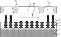
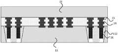
图2是在分离层上形成第一天线层、第一金属连接柱和第一封装层对应的结构示意图;2 is a schematic structural diagram corresponding to forming a first antenna layer, a first metal connection post and a first encapsulation layer on the separation layer;
图3是在第一玻璃基板上开设第一容置槽对应的结构示意图;3 is a schematic structural diagram corresponding to opening a first accommodating groove on the first glass substrate;
图4是将第一玻璃基板和分离层粘接并在第一容置槽内填充绝缘体对应的结构示意图;4 is a schematic structural diagram corresponding to bonding the first glass substrate and the separation layer and filling the insulator in the first accommodating groove;
图5是在第一玻璃基板上形成第二天线层和第二封装层对应的结构示意图;5 is a schematic structural diagram corresponding to forming a second antenna layer and a second encapsulation layer on the first glass substrate;
图6是剥离分离层后在第一天线层上接合射频芯片对应的结构示意图;6 is a schematic structural diagram corresponding to bonding a radio frequency chip on the first antenna layer after peeling off the separation layer;
图7是在第一天线层上接合射频芯片并在第一玻璃基板上开设第二容置槽对应的结构示意图;FIG. 7 is a schematic structural diagram corresponding to bonding a radio frequency chip on the first antenna layer and opening a second accommodating groove on the first glass substrate;
图8是将射频芯片内置于第一玻璃基板对应的结构示意图;FIG. 8 is a schematic structural diagram corresponding to the built-in radio frequency chip on the first glass substrate;
图9是形成第二金属连接柱和连接阻容器件对应的结构示意图;FIG. 9 is a schematic structural diagram corresponding to forming a second metal connecting post and connecting a resistance vessel;
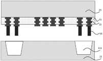
图10是形成第三封装层及焊球凸块的结构示意图;10 is a schematic structural diagram of forming a third packaging layer and solder ball bumps;
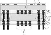
图11是本申请实施例二提供的天线的结构示意图;FIG. 11 is a schematic structural diagram of an antenna provided in Embodiment 2 of the present application;
图12是在第二玻璃基板上形成第二天线层、第一金属连接柱和第二封装层的结构示意图;12 is a schematic structural diagram of forming a second antenna layer, a first metal connecting post and a second encapsulation layer on a second glass substrate;
图13是将第一玻璃基板和第二玻璃基板粘接并在第一容置槽内填充绝缘体,并在第一金属连接柱对应位置开槽对应的结构示意图的结构示意图;13 is a schematic structural diagram of a structural schematic diagram corresponding to the first glass substrate and the second glass substrate being bonded, the insulator is filled in the first accommodating groove, and the corresponding position of the first metal connecting post is slotted;
图14是形成第一天线层、第一封装层、第三天线层和第四封装层对应的结构示意图;FIG. 14 is a schematic structural diagram corresponding to forming a first antenna layer, a first encapsulation layer, a third antenna layer and a fourth encapsulation layer;
图15是形成第二金属连接柱和接合射频芯片对应的结构示意图。FIG. 15 is a schematic diagram of the structure corresponding to forming the second metal connection post and bonding the radio frequency chip.
附图标记说明:Description of reference numbers:
11-第一玻璃基板;111-第一容置槽;112-绝缘体;113-第二容置槽;114-导电过孔;12-第一天线层;13-第二天线层;14-第一封装层;15-第二封装层;16-第一金属连接柱;17-射频芯片;18-第二金属连接柱;19-第三封装层;20-焊球凸块;21-金属球垫;22-阻容器件;23-第二玻璃基板;24-第三天线层;25-第四封装层;26-支撑基底;27-分离层。11-first glass substrate; 111-first accommodating slot; 112-insulator; 113-second accommodating slot; 114-conductive via; 12-first antenna layer; 13-second antenna layer; 14-th A packaging layer; 15- the second packaging layer; 16- the first metal connecting post; 17- the radio frequency chip; 18- the second metal connecting post; 19- the third packaging layer; 20- the solder ball bump; 21- the metal ball 22-resistance container; 23-second glass substrate; 24-third antenna layer; 25-fourth encapsulation layer; 26-support base; 27-separation layer.
具体实施方式Detailed ways
下面结合附图和具体实施例对本申请提供的天线、天线封装方法及终端进行说明。The antenna, the antenna packaging method and the terminal provided by the present application will be described below with reference to the accompanying drawings and specific embodiments.
实施例一Example 1
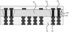
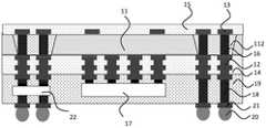
图1是本申请实施例一提供的天线的结构示意图一,参考图1所示,本申请实施例一提供的天线包括第一玻璃基板11、第一天线层12、第二天线层13、第一封装层14、第二封装层15和第一金属连接柱16。FIG. 1 is a schematic structural diagram 1 of an antenna provided by Embodiment 1 of the present application. Referring to FIG. 1 , the antenna provided by Embodiment 1 of the present application includes a
其中,第一玻璃基板11由玻璃制成的板状结构,第一玻璃基板11包括相对设置的第一表面和第二表面,第一表面为图1所示的第一玻璃基板11的下表面,第二表面为图1所示的第一玻璃基板11的上表面。第一玻璃基板11作为天线介质,其厚度为150μm-800μm,相比于采用塑封料作为天线介质,可降低介质厚度。The
本实施例中,采用第一玻璃基板11作为天线介质,相比于采用塑封料作为天线介质,可降低介电损耗,提高天线性能。且相比于塑封料,玻璃基板机械强度高、翘曲低、封装和后续上板加工难度低,失效风险低。In this embodiment, the
第一天线层12设置于第一玻璃基板11的第一表面,第二天线层13设置于第一玻璃基板11的第二表面。第一天线层12和第二天线层13均为金属布线层,其材料可以包括铜、镍、铝、金、银、钛中的一种或两种以上的组合。第一天线层12和第二天线层13可根据天线的性能需求,设置成各种不同的图形。The
在一种可能的实施方式中,第一天线层12和第二天线层13上均可以设置有重新布线层,重新布线层的厚度为3μm-10μm。重新布线层可实现高密度布线,减小天线互连的尺度和损耗,压缩互连空间,扩大天线设计的灵活性。In a possible implementation manner, both the
在上述实施例中,第一封装层14覆盖第一表面和第一天线层12,第二封装层15覆盖第二表面和第二天线层13。第一封装层14和第二封装层15可以包括环氧树脂、硅胶、聚酰亚胺PI中的一种,分别起到保护第一天线层12和第二天线层13的作用。In the above embodiment, the
第一玻璃基板11中设置有第一容置槽111,第一容置槽111为贯穿第一玻璃基板11的厚度方向的通孔。第一金属连接柱16设置于第一容置槽111内,第一金属连接柱16的两端分别与第一天线层12和第二天线层13连接;第一金属连接柱16的制作材料包括金、银、铜、铝中的至少一种,在一种可能的实施方式中,第一金属连接柱的制作材料与第一天线层12和第二天线层13的制作材料相同。第一容置槽111内设置由绝缘材料构成的绝缘体112,绝缘体112用于隔离第一金属连接柱112和第一玻璃基板11,防止第一金属连接柱112的侧面与第一玻璃基板11接触,防止第一金属连接柱112产生的热量直接传递到第一玻璃基板11上。The
需要说明的是,相关技术中,采用玻璃基板作为天线介质时,可直接在玻璃基板的设定区域开孔并在该开孔内电镀金属层作为金属连接柱,以连接位于玻璃基板两侧的天线层,但是,由于电镀金属层与玻璃基板直接接触,开孔位置容易出现玻璃开裂、金属残留等质量风险。并且,需要预先在玻璃生产厂家进行钻孔电镀工艺,再运输至封装厂家进行封装加工,如果天线的结构需要调整,则封装厂家需要向玻璃生产厂家重新订购玻璃原料,导致供应链复杂,生产周期长。It should be noted that, in the related art, when a glass substrate is used as the antenna medium, a hole can be directly opened in a set area of the glass substrate and a metal layer can be plated in the opening as a metal connection column to connect the two sides of the glass substrate. However, due to the direct contact between the electroplated metal layer and the glass substrate, quality risks such as glass cracking and metal residue are prone to occur at the opening position. In addition, the drilling and electroplating process needs to be carried out in the glass manufacturer in advance, and then transported to the packaging manufacturer for packaging processing. If the structure of the antenna needs to be adjusted, the packaging manufacturer needs to re-order the glass raw material from the glass manufacturer, resulting in a complicated supply chain and a production cycle. long.
而本实施例中,通过在第一玻璃基板上开设第一容置槽111,在第一容置槽111内填充绝缘体112,将第一金属连接柱16设置在绝缘体112中,从而避免了第一金属连接柱16直接与第一容置槽111的壁面接触,不容易出现玻璃开裂、金属残留的质量风险。且该工艺可以在封装厂家直接进行,调整天线结构时,无需重新订购玻璃原料,从而节约了生产周期。In this embodiment, the first
上述图1所示的天线,可采用如下制作方法制作形成:The above-mentioned antenna shown in FIG. 1 can be formed by the following manufacturing method:
首先,提供支撑基底26,支撑基底26上设置有分离层27。First, the
作为示例,支撑基底26包括玻璃衬底、金属衬底、半导体衬底、聚合物衬底及陶瓷衬底中的一种。其中,采用玻璃衬底作为支撑基底26,具有成本低,容易在表面形成分离层,且能降低后续剥离工艺的难度的优点。作为示例,分离层27包括胶带及聚合物层中的一种,聚合物层可采用旋涂工艺涂覆于支撑基底26的表面,然后采用紫外固化或者热固化工艺使其固化成型。As an example, the
参考图2所示,接下来,在分离层27上形成第一天线层12,并在第一天线层12上形成第一金属连接柱16。可采用化学气相沉积工艺、蒸镀工艺、溅射工艺、电镀工艺或化学镀工艺在分离层27上形成金属层,可通过对金属层进行刻蚀以形成图形化的第一天线层12和第一金属连接柱16,其中,第一金属连接柱16的下端与第一天线层12连接。Referring to FIG. 2 , next, the
接着,形成覆盖第一天线层12的第一封装层14,第一金属连接柱16远离分离层27的一端暴露在第一封装层14外。其中,第一封装层14可采用压缩成型、传递模塑成型、液封成型、真空层压及旋涂等工艺形成。Next, a
参考图3所示,接下来,提供第一玻璃基板11,第一玻璃基板11中设置有第一容置槽111。其中,第一容置槽111的位置和第一金属连接柱16的位置对应。第一玻璃基板11的厚度与天线结构相关,第一容置槽111可以为直接在第一玻璃基板11上开设的通孔,也可先在第一玻璃基板11上开盲孔,再将第一玻璃基板11研磨减薄,直至露出盲孔的底部,形成通孔。第一容置槽111可以通过蚀刻或者激光加工形成,第一容置槽111的直径大于第一金属连接柱16的直径。Referring to FIG. 3 , next, a
参考图4所示,接着,将第一玻璃基板11粘接在分离层27上,第一金属连接柱16放置于第一容置槽111内,并使用绝缘材料填充第一容置槽111以形成绝缘体112。其中,绝缘材料可以为环氧树脂、硅胶、聚酰亚胺PI中的一种,绝缘材料填充在第一容置槽111内后,可隔离第一金属连接柱16和第一容置槽111的内壁面,防止第一金属连接柱16影响到第一玻璃基板11的机械性能。Referring to FIG. 4 , next, the
在另一种可能的实施方式中,第一金属连接柱16也可以在形成绝缘体112后,通过在绝缘体112中开孔并进行电镀形成,此时,绝缘体112是便于加工开孔的环氧树脂等材料。In another possible implementation manner, the first
参考图5所示,接下来,在第一玻璃基板11的远离支撑基底26的表面上形成第二天线层13,以及形成覆盖第二天线层13的第二封装层15,第二天线层13和第一金属连接柱16电连接。其中,可采用化学气相沉积工艺、蒸镀工艺、溅射工艺、电镀工艺或化学镀工艺在第一玻璃基板11的表面上形成金属层,可通过对金属层进行刻蚀以形成图形化的第二天线层13。第二封装层15可采用压缩成型、传递模塑成型、液封成型、真空层压及旋涂等工艺形成。5, next, the
在一种可能的实施方式中,将第一玻璃基板11和绝缘体112研磨减薄,以使第一金属连接柱16的端部暴露在绝缘体112的表面,以使第二天线层13和暴露在绝缘体112表面的第一金属连接柱16直接连接。In a possible implementation manner, the
在另一种可能的实施方式中,也可在绝缘体112上设置多个过孔,形成第二天线层13时,过孔被金属材料填充形成导电过孔,第二天线层13通过导电过孔与第一金属连接柱16连接。In another possible implementation manner, a plurality of via holes may also be provided on the
最后,剥离分离层27和支撑基底26。其中,分离层27可以为光热转换层,可通过激光对光热转换成进行加热,以使分离层27和支撑基底26与第一天线层12相互分离,形成如图1所示的天线。Finally, the
需要注意的是,本实施例提供的天线,可通过刷锡膏的方式与电路板互连,且可通过电路板外接射频芯片,以实现天线功能。It should be noted that the antenna provided in this embodiment can be interconnected with the circuit board by brushing solder paste, and an external radio frequency chip can be connected through the circuit board to realize the antenna function.
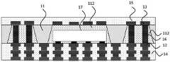
射频芯片也可直接设置在天线内,图6是剥离分离层后在第一天线层上接合射频芯片对应的结构示意图,参考图6所示,在一种可能的实施方式中,本实施例提供的天线还包括:与第一天线层12电连接的射频芯片17,射频芯片17设置于第一天线层12的远离第一玻璃基板11的表面。射频芯片17一方面和第一天线层12电连接,另一方面与电路板连接。The radio frequency chip can also be directly arranged in the antenna. FIG. 6 is a schematic diagram of the structure corresponding to bonding the radio frequency chip on the first antenna layer after peeling off the separation layer. Referring to FIG. 6 , in a possible implementation, this embodiment provides The antenna further includes: a
图6提供的天线结构的具体制作方法为,在剥离分离层27和支撑基底26的步骤后,在第一天线层12的远离第一玻璃基板11的表面上接合射频芯片17,射频芯片17和第一天线层12电连接。The specific manufacturing method of the antenna structure provided in FIG. 6 is as follows: after the step of peeling off the
图7是在第一天线层上接合射频芯片并在第一玻璃基板上开设第二容置槽对应的结构示意图,图8是将射频芯片内置于第一玻璃基板对应的结构示意图,参考图7和图8所示,在另一种可能的实施方式中,第一玻璃基板11内设置有第二容置槽113,射频芯片17位于第二容置槽113内。将射频芯片17内置于第一玻璃基板11内,可进一步降低天线结构整体的厚度。FIG. 7 is a schematic structural diagram corresponding to bonding a radio frequency chip on the first antenna layer and opening a second accommodating groove on the first glass substrate. FIG. 8 is a structural schematic diagram corresponding to embedding the radio frequency chip on the first glass substrate. Refer to FIG. 7 As shown in FIG. 8 , in another possible implementation manner, the
其中,将射频芯片17内置于第一玻璃基板11内的制作方法如下:在图2的基础上,在分离层27上形成第一天线层12后,接着在第一天线层12上连接射频芯片17;在图3的基础上,提供第一玻璃基板11的步骤之后,在第一玻璃基板11上开设第二容置槽113;如图7所示,在将第一玻璃基板11粘接在分离层27上时,将射频芯片17放置于第二容置槽113内,并使用绝缘材料填充第二容置槽113以形成绝缘体112。Wherein, the manufacturing method of embedding the
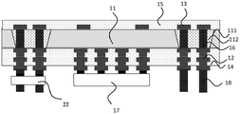
图9是形成第二金属连接柱和连接阻容器件对应的结构示意图,图10是形成第三封装层及焊球凸块的结构示意图,参考图9和图10所示,在图6的基础上,本实施例中,天线还包括第三封装层19。第三封装层19覆盖射频芯片17,第三封装层19可以包括环氧树脂、硅胶、聚酰亚胺PI中的一种,起到保护射频芯片17的作用。9 is a schematic diagram of the structure corresponding to the formation of the second metal connection post and the connection resistance device, and FIG. 10 is a schematic diagram of the structure of the formation of the third packaging layer and the solder ball bumps. Referring to FIG. 9 and FIG. 10 , on the basis of FIG. 6 Above, in this embodiment, the antenna further includes a
其中,同时,在覆盖了第三封装层19后,为了使第一天线层12和射频芯片17可以与外部电路板连接,本实施例中,在第一天线层12上设置了第二金属连接柱18。第二金属连接柱18设置于第一天线层12的远离第一玻璃基板11的表面,第二金属连接柱18制作材料包括金、银、铜、铝中的一种。第二金属连接柱18的端部暴露在第三封装层19外,或者,可以在第三封装层19上设置导电过孔,以使第二金属连接柱18可与外部电路板连通。Meanwhile, after the
为了保证天线和电路板的连接的可靠性,本实施例中,天线还包括焊球凸块20,焊球凸块20设置在第三封装层19的远离第一玻璃基板11的表面,且焊球凸块20通过金属球垫21和第二金属连接柱18连接。焊球凸块20包括锡焊料、银焊料及金锡合金焊料中的一种。In order to ensure the reliability of the connection between the antenna and the circuit board, in this embodiment, the antenna further includes solder ball bumps 20 . The solder ball bumps 20 are arranged on the surface of the
本实施例中,天线还包括阻容器件22,阻容器件22设置在第三封装层19内,并与第一天线层12电连接。阻容器件22可起到降低干扰的作用,需要说明的是,在第一天线层12和射频芯片17的连接线路之间还可以增加滤波电路,滤波电路和阻容器件22共同起到降低干扰、提高天线性能的作用。In this embodiment, the antenna further includes a
上述实施例中,在图6的基础上继续形成第二金属连接柱18、阻容器件22、第三封装层19和焊球凸块20的制作方法可以为:首先,在第一天线层12的远离第一玻璃基板11的表面上形成第二金属连接柱18和阻容器件22;接着,形成覆盖射频芯片17、第二金属连接柱18和阻容器件22的第三封装层19,第二金属连接柱18远离第一玻璃基板11的一端暴露在第三封装层19外;接着,在第三封装层19上形成金属球垫21,金属球垫21和第二金属连接柱18电连接;最后,在金属球垫21上形成焊球凸块20。In the above-mentioned embodiment, on the basis of FIG. 6 , the manufacturing method of continuing to form the second
本申请实施例一提供的天线,设置第一玻璃基板作为天线介质,相比于采用塑封料作为介质,玻璃材质的第一玻璃基板的介电损耗低,天线增益高,可有效缩小封装体积。另外,第一玻璃基板上下表面的天线金属层通过第一金属连接柱连接,第一金属连接柱和第一玻璃基板之间填充有绝缘体,可避免第一金属连接柱与第一玻璃基板直接接触,可防止第一玻璃基板在温度变化时开裂。此外,第一玻璃基板上的开槽和第一金属连接柱的设计解耦,第一金属连接柱的直径以及第一容置槽在第一玻璃基板中的位置调整不需要玻璃厂商的配合,可大大缩短天线设计的开发周期和重复玻璃基板打样的成本。In the antenna provided in the first embodiment of the present application, the first glass substrate is set as the antenna medium. Compared with the use of plastic sealing compound as the medium, the first glass substrate made of glass has lower dielectric loss and higher antenna gain, which can effectively reduce the package volume. In addition, the antenna metal layers on the upper and lower surfaces of the first glass substrate are connected by first metal connecting posts, and an insulator is filled between the first metal connecting posts and the first glass substrate to avoid direct contact between the first metal connecting posts and the first glass substrate , which can prevent the first glass substrate from cracking when the temperature changes. In addition, the design of the slot on the first glass substrate is decoupled from the design of the first metal connecting column, and the adjustment of the diameter of the first metal connecting column and the position of the first accommodating groove in the first glass substrate does not require the cooperation of the glass manufacturer. It can greatly shorten the development cycle of antenna design and the cost of repeated glass substrate proofing.
实施例二Embodiment 2
图11是本申请实施例二提供的天线的结构示意图,参考图11所示,本申请实施例二提供的天线包括:第一玻璃基板11、第一天线层12、第二天线层13、第一封装层14、第二封装层15、第一金属连接柱16、射频芯片17、第二金属连接柱18、第三封装层19、焊球凸块20、第二玻璃基板23、第三天线层24和第四封装层25。FIG. 11 is a schematic structural diagram of the antenna provided by the second embodiment of the present application. Referring to FIG. 11 , the antenna provided by the second embodiment of the present application includes: a
其中,第一玻璃基板11和第二玻璃基板23均为由玻璃制成的板状结构,第一玻璃基板11包括相对设置的第一表面和第二表面,第一表面为图11所示的第一玻璃基板11的下表面,第二表面为图11所示的第一玻璃基板11的上表面。第一玻璃基板11和第二玻璃基板23作为天线介质,其厚度为150μm-800μm,相比于采用塑封料作为天线介质,可降低介质厚度。Wherein, the
本实施例中,采用第一玻璃基板11和第二玻璃基板23作为天线介质,相比于采用塑封料作为天线介质,可降低介电损耗,提高天线性能。且相比于塑封料,玻璃基板机械强度高、翘曲低、封装和后续上板加工难度低,失效风险低。In this embodiment, the
第一天线层12设置于第一玻璃基板11的第一表面,第二天线层13设置于第一玻璃基板11的第二表面,第三天线层24设置于第二玻璃基板23的远离第一玻璃基板11的表面上。第一天线层12、第二天线层13和第三天线层24均为金属布线层,其材料可以包括铜、镍、铝、金、银、钛中的一种或两种以上的组合,并可根据天线的性能需求,设置成各种不同的图形。The
在一种可能的实施方式中,第一天线层12、第二天线层13和第三天线层24上均可以设置有重新布线层,重新布线层的厚度为3μm-10μm。重新布线层可实现高密度布线,减小天线互连的尺度和损耗,压缩互连空间,扩大天线设计的灵活性。In a possible implementation manner, the
其中,第一封装层14覆盖第一表面和第一天线层12,第二封装层15覆盖第二表面和第二天线层13,第四封装层25覆盖第二玻璃基板23的远离第一玻璃基板11的表面及第三天线层24。第一封装层14、第二封装层15和第四封装层25均可以包括环氧树脂、硅胶、聚酰亚胺PI中的一种,分别起到保护第一天线层12、第二天线层13和第三天线层24的作用。The
第一玻璃基板11中设置有第一容置槽111,第一容置槽111内设置有绝缘体112,第一金属连接柱16设置于绝缘体112中,且第一金属连接柱16的两端分别与第一天线层12和第二天线层13连接。第一金属连接柱16的制作材料包括金、银、铜、铝中的一种,设置于第一容置槽111内,第一金属连接柱16的两端分别与第一天线层12和第二天线层13连接。第一容置槽111为贯穿第一玻璃基板11的厚度方向的通孔,第一容置槽111内设置由绝缘材料构成的绝缘体112,绝缘体112用于隔离第一金属连接柱112和第一玻璃基板11,防止第一金属连接柱112的侧面与第一玻璃基板11接触,防止第一金属连接柱112影响第一玻璃基板11的机械性能。A first
本实施例中,射频芯片17设置于第一天线层12的远离第一玻璃基板11的表面,且与第一天线层12电连接。射频芯片17一方面和第一天线层12电连接,另一方面与电路板连接。In this embodiment, the
此外,第二金属连接柱18设置于第一天线层12的远离第一玻璃基板11的表面,第三封装层19覆盖射频芯片17和第二金属连接柱18,且第三封装层19的远离第一玻璃基板11的表面上暴露出第二金属连接柱18的端部。In addition, the second
焊球凸块20设置在第三封装层19的远离第一玻璃基板11的表面,且焊球凸块20通过金属球垫21和第二金属连接柱18连接。The solder ball bumps 20 are disposed on the surface of the
在一种可能的实施方式中,图11提供的天线结构可采用以下制作方法制作而成:In a possible implementation manner, the antenna structure provided in FIG. 11 can be fabricated by the following fabrication methods:
在实施例一所述的天线制作方法的基础上,提供第二玻璃基板23;将第二玻璃基板23粘接在第二封装层15上;在第二玻璃基板23的远离第一玻璃基板11的表面上形成第三天线层24,以及形成覆盖第三天线层24的第四封装层25。On the basis of the antenna manufacturing method described in the first embodiment, a
在另一种可能的实施方式中,图11提供的天线结构,可采用以下步骤制作而成:In another possible implementation manner, the antenna structure provided in FIG. 11 can be fabricated by using the following steps:
首先,提供第一玻璃基板11和第二玻璃基板23。First, the
参考图12所示,接下来,可在第二玻璃基板23上形成第二天线层13和位于第二天线层13上的第一金属连接柱16,以及形成覆盖第二天线层13的第二封装层15。其中,可采用化学气相沉积工艺、蒸镀工艺、溅射工艺、电镀工艺或化学镀工艺在第二玻璃基板23上形成金属层,可通过对金属层进行刻蚀以形成图形化的第二天线层13和第一金属连接柱16。第二封装层15可采用压缩成型、传递模塑成型、液封成型、真空层压及旋涂等工艺形成。Referring to FIG. 12 , next, the
然后,可在第一玻璃基板11中开设第一容置槽111,其中,第一容置槽111的位置和第一金属连接柱16的位置对应。第一容置槽111可以为直接在第一玻璃基板11上开设的通孔,也可先在第一玻璃基板11上开盲孔,再将第一玻璃基板11研磨减薄,直至露出盲孔的底部,形成通孔。Then, a first
参考图13所示,下一步,可将第一玻璃基板11粘接在第二玻璃基板23上,第一金属连接柱16插装在第一容置槽111内;并使用绝缘材料填充满第一容置槽111以形成绝缘体112。Referring to FIG. 13 , in the next step, the
绝缘材料可以为环氧树脂、硅胶、聚酰亚胺PI中的一种,绝缘材料填充在第一容置槽111内后,可隔离第一金属连接柱16和第一容置槽111的内壁面,防止第一金属连接柱16影响到第一玻璃基板11的机械性能。The insulating material can be one of epoxy resin, silica gel, and polyimide PI. After the insulating material is filled in the first
在另一种可能的实施方式中,第一金属连接柱16也可以在形成绝缘体112后,通过在绝缘体112中开孔并进行电镀形成,此时,绝缘体112是便于加工开孔的环氧树脂等材料。In another possible implementation manner, the first
参考图14所示,接下来,可在第一玻璃基板11的远离第二玻璃基板23的表面上形成第一天线层12,以及形成覆盖第一天线层12的第一封装层14;在第二玻璃基板23的远离第一玻璃基板11的表面上形成第三天线层24,以及形成覆盖第三天线层24的第四封装层25。Referring to FIG. 14, next, the
其中,可采用化学气相沉积工艺、蒸镀工艺、溅射工艺、电镀工艺或化学镀工艺在第一玻璃基板11的表面上形成金属层,可通过对金属层进行刻蚀以形成图形化的第一天线层12。同样地,可在第二玻璃基板23的表面上形成第三天线层24。第一封装层14和第四封装层25均可采用压缩成型、传递模塑成型、液封成型、真空层压及旋涂等工艺形成,以分别起到保护第一天线层12和第三天线层24的作用。Wherein, chemical vapor deposition process, evaporation process, sputtering process, electroplating process or chemical plating process can be used to form a metal layer on the surface of the
为了实现第二天线层13和第一金属连接柱14的连接,在形成绝缘体112后,可以通过将第一玻璃基板11和绝缘体112研磨减薄,使第一金属连接柱16的端部暴露在绝缘体112的表面,以使第二天线层13和暴露在绝缘体112表面的第一金属连接柱16直接连接。或者,在形成绝缘体112后,也可在绝缘体112上设置多个过孔,形成第二天线层13时,过孔被金属材料填充形成导电过孔114,第二天线层13通过导电过孔114与第一金属连接柱16连接。参考图15所示,接下来,可在第一天线层12的远离第一玻璃基板11的表面上形成连接射频芯片17,并在第一天线层12的远离第一玻璃基板11的表面上形成第二金属连接柱18,再形成覆盖射频芯片17和第一天线层12的远离第一玻璃基板11的表面的第三封装层19,第二金属连接柱18远离第一玻璃基板11的一端暴露在第三封装层19外。In order to realize the connection between the
其中,第三封装层19可以包括环氧树脂、硅胶、聚酰亚胺PI中的一种,起到保护射频芯片17的作用。同时,在覆盖了第三封装层19后,为了使第一天线层12和射频芯片17可以与外部电路板连接,本实施例中,在第一天线层12上设置了第二金属连接柱18,第二金属连接柱18制作材料包括金、银、铜、铝中的一种。第二金属连接柱18的端部暴露在第三封装层19外,或者,可以在第三封装层19上设置导电过孔,以使第二金属连接柱18可与外部电路板连通。Wherein, the
最后,参考图11所示,可在第三封装层19上形成金属球垫21,金属球垫21和第二金属连接柱18电连接;并在金属球垫21上形成焊球凸块20。Finally, as shown in FIG. 11 ,
本申请实施例二提供的天线,设置第一玻璃基板和第二玻璃基板作为天线介质,相比于采用塑封料作为介质,介电损耗低、天线增益高,可有效缩小封装体积。第一金属连接柱和第一玻璃基板之间填充有绝缘体,可避免第一金属连接柱与第一玻璃基板直接接触,可防止第一玻璃基板在温度变化时开裂。此外,第一玻璃基板上的开槽和第一金属连接柱的设计解耦,第一金属连接柱的直径以及第一容置槽在第一玻璃基板中的位置调整不需要玻璃厂商的配合,可大大缩短天线设计的开发周期和重复玻璃基板打样的成本。In the antenna provided in the second embodiment of the present application, the first glass substrate and the second glass substrate are set as the antenna medium. Compared with the use of plastic sealing compound as the medium, the dielectric loss is low and the antenna gain is high, which can effectively reduce the package volume. An insulator is filled between the first metal connection post and the first glass substrate, which can avoid direct contact between the first metal connection post and the first glass substrate and prevent the first glass substrate from cracking when the temperature changes. In addition, the design of the slot on the first glass substrate and the design of the first metal connecting column are decoupled, and the adjustment of the diameter of the first metal connecting column and the position of the first accommodating groove in the first glass substrate does not require the cooperation of the glass manufacturer. It can greatly shorten the development cycle of antenna design and the cost of repeated glass substrate proofing.
实施例三Embodiment 3
本申请实施例三提供一种终端,包括:电路板以及如上实施例一或二提供的天线,该天线与电路板连接。其中,本申请实施例三涉及的终端设备可以包括手机、手表、平板电脑、个人数字助理(Personal Digital Assistant,PDA)、销售终端(Point of Sales,POS)、车载电脑等电子设备。Embodiment 3 of the present application provides a terminal, including: a circuit board and the antenna provided in Embodiment 1 or 2 above, where the antenna is connected to the circuit board. The terminal device involved in Embodiment 3 of the present application may include electronic devices such as a mobile phone, a watch, a tablet computer, a Personal Digital Assistant (PDA), a Point of Sales (POS), and a vehicle-mounted computer.
本申请实施例三提供的终端中,包括上述实施例一或实施例二提供的天线,因此也具有上述实施例一或实施例二所述的优点,具体可参考上面相关描述,在此不再赘述。The terminal provided in Embodiment 3 of this application includes the antenna provided in Embodiment 1 or Embodiment 2 above, and therefore also has the advantages described in Embodiment 1 or Embodiment 2 above. For details, please refer to the relevant description above, which is omitted here. Repeat.
本申请的说明书中各实施例或实施方式采用递进的方式描述,每个实施例重点说明的都是与其他实施例的不同之处,各个实施例之间相同相似部分相互参见即可。The embodiments or implementations in the specification of the present application are described in a progressive manner, and each embodiment focuses on the differences from other embodiments, and the same and similar parts between the various embodiments may be referred to each other.
在本申请的说明书的描述中,参考术语“一个实施方式”、“一些实施方式”、“示意性实施方式”、“示例”、“具体示例”、或“一些示例”等的描述意指结合实施方式或示例描述的具体特征、结构、材料或者特点包含于本申请的至少一个实施方式或示例中。在本说明书中,对上述术语的示意性表述不一定指的是相同的实施方式或示例。而且,描述的具体特征、结构、材料或者特点可以在任何的一个或多个实施方式或示例中以合适的方式结合。In the description of the specification of the present application, reference to the description of the terms "one embodiment", "some embodiments", "exemplary embodiment", "example", "specific example", or "some examples", etc., is intended to combine A particular feature, structure, material, or characteristic described by an embodiment or example is included in at least one embodiment or example of this application. In this specification, schematic representations of the above terms do not necessarily refer to the same embodiment or example. Furthermore, the particular features, structures, materials or characteristics described may be combined in any suitable manner in any one or more embodiments or examples.
最后应说明的是:以上各实施例仅用以说明本申请的技术方案,而非对其限制;尽管参照前述各实施例对本申请进行了详细的说明,本领域的普通技术人员应当理解:其依然可以对前述各实施例所记载的技术方案进行修改,或者对其中部分或者全部技术特征进行等同替换;而这些修改或者替换,并不使相应技术方案的本质脱离本申请各实施例技术方案的范围。Finally, it should be noted that the above embodiments are only used to illustrate the technical solutions of the present application, but not to limit them; although the present application has been described in detail with reference to the foregoing embodiments, those of ordinary skill in the art should understand that: The technical solutions described in the foregoing embodiments can still be modified, or some or all of the technical features thereof can be equivalently replaced; and these modifications or replacements do not make the essence of the corresponding technical solutions deviate from the technical solutions of the embodiments of the present application. scope.
Claims (15)
Priority Applications (2)
| Application Number | Priority Date | Filing Date | Title |
|---|---|---|---|
| CN201911007437.7ACN112701444B (en) | 2019-10-22 | 2019-10-22 | Antenna, antenna packaging method and terminal |
| PCT/CN2020/120552WO2021078038A1 (en) | 2019-10-22 | 2020-10-13 | Antenna, antenna encapsulating method and terminal |
Applications Claiming Priority (1)
| Application Number | Priority Date | Filing Date | Title |
|---|---|---|---|
| CN201911007437.7ACN112701444B (en) | 2019-10-22 | 2019-10-22 | Antenna, antenna packaging method and terminal |
Publications (2)
| Publication Number | Publication Date |
|---|---|
| CN112701444A CN112701444A (en) | 2021-04-23 |
| CN112701444Btrue CN112701444B (en) | 2022-06-28 |
Family
ID=75504603
Family Applications (1)
| Application Number | Title | Priority Date | Filing Date |
|---|---|---|---|
| CN201911007437.7AExpired - Fee RelatedCN112701444B (en) | 2019-10-22 | 2019-10-22 | Antenna, antenna packaging method and terminal |
Country Status (2)
| Country | Link |
|---|---|
| CN (1) | CN112701444B (en) |
| WO (1) | WO2021078038A1 (en) |
Families Citing this family (2)
| Publication number | Priority date | Publication date | Assignee | Title |
|---|---|---|---|---|
| CN115623677B (en)* | 2021-07-14 | 2025-09-23 | 鹏鼎控股(深圳)股份有限公司 | Antenna packaging structure and manufacturing method thereof |
| US20240283130A1 (en)* | 2023-02-21 | 2024-08-22 | Tron Future Tech Inc. | Antenna package and method for manufacturing an antenna package |
Citations (5)
| Publication number | Priority date | Publication date | Assignee | Title |
|---|---|---|---|---|
| CN103797498A (en)* | 2011-09-12 | 2014-05-14 | 日立化成株式会社 | RFID tags and automatic identification systems |
| CN108305856A (en)* | 2018-03-16 | 2018-07-20 | 中芯长电半导体(江阴)有限公司 | The encapsulating structure and packaging method of antenna |
| CN109149069A (en)* | 2018-08-12 | 2019-01-04 | 瑞声科技(南京)有限公司 | AOG antenna system and mobile terminal |
| CN109768031A (en)* | 2019-03-04 | 2019-05-17 | 中芯长电半导体(江阴)有限公司 | Antenna packaging structure and packaging method |
| CN110120385A (en)* | 2019-06-03 | 2019-08-13 | 中芯长电半导体(江阴)有限公司 | Semiconductor package and preparation method thereof |
Family Cites Families (9)
| Publication number | Priority date | Publication date | Assignee | Title |
|---|---|---|---|---|
| JP2002073210A (en)* | 2000-08-31 | 2002-03-12 | Toshiba Corp | Portable information equipment with built-in wireless communication antenna |
| WO2004109771A2 (en)* | 2003-06-03 | 2004-12-16 | Casio Computer Co., Ltd. | Stackable semiconductor device and method of manufacturing the same |
| JP4908899B2 (en)* | 2006-04-07 | 2012-04-04 | ラピスセミコンダクタ株式会社 | Semiconductor device and manufacturing method thereof |
| EP1988575A3 (en)* | 2007-03-26 | 2008-12-31 | Semiconductor Energy Laboratory Co., Ltd. | Semiconductor device |
| KR20100118350A (en)* | 2009-04-28 | 2010-11-05 | 엘지이노텍 주식회사 | Antenna of broadcasting receiver |
| CN103633443B (en)* | 2013-08-13 | 2016-05-25 | 北京航空航天大学 | Multiband Wideband Small-sized Planar Monopole Antenna |
| US10325786B1 (en)* | 2017-12-07 | 2019-06-18 | Sj Semiconductor (Jiangyin) Corporation | Double-sided plastic fan-out package structure having antenna and manufacturing method thereof |
| TWI745515B (en)* | 2017-12-22 | 2021-11-11 | 啟耀光電股份有限公司 | Electronic device and manufacturing method thereof |
| CN108336494B (en)* | 2018-03-16 | 2022-03-01 | 盛合晶微半导体(江阴)有限公司 | Antenna packaging structure and packaging method |
- 2019
- 2019-10-22CNCN201911007437.7Apatent/CN112701444B/ennot_activeExpired - Fee Related
- 2020
- 2020-10-13WOPCT/CN2020/120552patent/WO2021078038A1/ennot_activeCeased
Patent Citations (5)
| Publication number | Priority date | Publication date | Assignee | Title |
|---|---|---|---|---|
| CN103797498A (en)* | 2011-09-12 | 2014-05-14 | 日立化成株式会社 | RFID tags and automatic identification systems |
| CN108305856A (en)* | 2018-03-16 | 2018-07-20 | 中芯长电半导体(江阴)有限公司 | The encapsulating structure and packaging method of antenna |
| CN109149069A (en)* | 2018-08-12 | 2019-01-04 | 瑞声科技(南京)有限公司 | AOG antenna system and mobile terminal |
| CN109768031A (en)* | 2019-03-04 | 2019-05-17 | 中芯长电半导体(江阴)有限公司 | Antenna packaging structure and packaging method |
| CN110120385A (en)* | 2019-06-03 | 2019-08-13 | 中芯长电半导体(江阴)有限公司 | Semiconductor package and preparation method thereof |
Also Published As
| Publication number | Publication date |
|---|---|
| WO2021078038A1 (en) | 2021-04-29 |
| CN112701444A (en) | 2021-04-23 |
Similar Documents
| Publication | Publication Date | Title |
|---|---|---|
| US11222852B2 (en) | Method for fabricating electronic package | |
| US12388032B2 (en) | Semiconductor device with redistribution layers formed utilizing dummy substrates | |
| EP2798675B1 (en) | Method for a substrate core layer | |
| CN108305856B (en) | Antenna packaging structure and packaging method | |
| KR101605600B1 (en) | Manufacturing method of semiconductor device and semiconductor device thereof | |
| US20080315396A1 (en) | Mold compound circuit structure for enhanced electrical and thermal performance | |
| US8841759B2 (en) | Semiconductor package and manufacturing method thereof | |
| CN110085973B (en) | Antenna packaging structure and packaging method | |
| TWI264744B (en) | Solid electrolytic capacitor, transmission-line device, method of producing the same, and composite electronic component using the same | |
| US20180331027A1 (en) | Electronic package and method for fabricating the same | |
| CN112599499B (en) | Antenna packaging structure and packaging method | |
| CN112310061B (en) | Semiconductor packaging structure | |
| US20100190294A1 (en) | Methods for controlling wafer and package warpage during assembly of very thin die | |
| WO2017113921A1 (en) | Frame package structure of integrated passive device and manufacturing method thereof | |
| CN111799181B (en) | Electronic package and manufacturing method thereof | |
| CN111199957A (en) | Three-dimensional packaging structure integrating chip and antenna and preparation method thereof | |
| CN112701444B (en) | Antenna, antenna packaging method and terminal | |
| CN108962878B (en) | Electronic package and manufacturing method thereof | |
| KR101341619B1 (en) | Semiconductor package and method for manufacturing semiconductor package | |
| CN112289766B (en) | Packaged antenna module and preparation method thereof | |
| CN102024798A (en) | Packaging structure for integrating surface mounting type assembly | |
| TW201633455A (en) | Package substrate, package structure including the same, and their fabrication methods | |
| CN114823557A (en) | Fan-out type double-sided packaging structure and preparation method thereof | |
| TW202247302A (en) | Antenna package and method for manufacturing the same | |
| CN101226918A (en) | Chip packaging substrate and packaging structure thereof |
Legal Events
| Date | Code | Title | Description |
|---|---|---|---|
| PB01 | Publication | ||
| PB01 | Publication | ||
| SE01 | Entry into force of request for substantive examination | ||
| SE01 | Entry into force of request for substantive examination | ||
| GR01 | Patent grant | ||
| GR01 | Patent grant | ||
| CF01 | Termination of patent right due to non-payment of annual fee | ||
| CF01 | Termination of patent right due to non-payment of annual fee | Granted publication date:20220628 |