CN112683332B - Multi-physical-parameter wide-field quantum camera based on ensemble nitrogen atom-vacancy color center - Google Patents
Multi-physical-parameter wide-field quantum camera based on ensemble nitrogen atom-vacancy color centerDownload PDFInfo
- Publication number
- CN112683332B CN112683332BCN202011585896.6ACN202011585896ACN112683332BCN 112683332 BCN112683332 BCN 112683332BCN 202011585896 ACN202011585896 ACN 202011585896ACN 112683332 BCN112683332 BCN 112683332B
- Authority
- CN
- China
- Prior art keywords
- microwave
- ensemble
- diamond
- magnetic field
- fluorescence
- Prior art date
- Legal status (The legal status is an assumption and is not a legal conclusion. Google has not performed a legal analysis and makes no representation as to the accuracy of the status listed.)
- Active
Links
- IJGRMHOSHXDMSA-UHFFFAOYSA-NAtomic nitrogenChemical groupN#NIJGRMHOSHXDMSA-UHFFFAOYSA-N0.000titleclaimsdescription16
- 229910052757nitrogenInorganic materials0.000titleclaimsdescription8
- 229910003460diamondInorganic materials0.000claimsabstractdescription41
- 239000010432diamondSubstances0.000claimsabstractdescription41
- 238000003384imaging methodMethods0.000claimsabstractdescription20
- 238000012545processingMethods0.000claimsabstractdescription17
- 230000010287polarizationEffects0.000claimsabstractdescription14
- 230000005855radiationEffects0.000claimsdescription10
- 230000003321amplificationEffects0.000claimsdescription3
- 238000003199nucleic acid amplification methodMethods0.000claimsdescription3
- 230000005415magnetizationEffects0.000claimsdescription2
- 229910001172neodymium magnetInorganic materials0.000claimsdescription2
- QJVKUMXDEUEQLH-UHFFFAOYSA-N[B].[Fe].[Nd]Chemical compound[B].[Fe].[Nd]QJVKUMXDEUEQLH-UHFFFAOYSA-N0.000claims1
- 230000005540biological transmissionEffects0.000claims1
- 230000003287optical effectEffects0.000abstractdescription22
- 238000001514detection methodMethods0.000abstractdescription16
- 238000000387optically detected magnetic resonanceMethods0.000abstractdescription10
- 238000005516engineering processMethods0.000description7
- 238000010586diagramMethods0.000description6
- 230000005284excitationEffects0.000description5
- 238000012360testing methodMethods0.000description4
- 230000005283ground stateEffects0.000description3
- 238000005259measurementMethods0.000description3
- 238000000034methodMethods0.000description3
- 230000035945sensitivityEffects0.000description3
- 230000007547defectEffects0.000description2
- 230000001419dependent effectEffects0.000description2
- 238000004435EPR spectroscopyMethods0.000description1
- 125000004432carbon atomChemical groupC*0.000description1
- 238000012512characterization methodMethods0.000description1
- 239000013078crystalSubstances0.000description1
- 238000011161developmentMethods0.000description1
- 238000005485electric heatingMethods0.000description1
- 230000005281excited stateEffects0.000description1
- 238000001914filtrationMethods0.000description1
- 230000001678irradiating effectEffects0.000description1
- 238000005404magnetometryMethods0.000description1
- 238000012544monitoring processMethods0.000description1
- 125000004433nitrogen atomChemical groupN*0.000description1
- -1nitrogen-substituted carbon atomChemical group0.000description1
- 238000001228spectrumMethods0.000description1
Images


Landscapes
- Investigating, Analyzing Materials By Fluorescence Or Luminescence (AREA)
Abstract
Description
Translated fromChinese技术领域technical field
本发明涉及量子传感与精密测量技术领域,具体为一种基于系综金刚石氮空位(Nitrogen-Vacancy,NV)色心的能进行磁场、温度等多物理参数实时成像的微米空间分辨率的宽场量子相机。The invention relates to the technical field of quantum sensing and precision measurement, specifically a wide micron spatial resolution based on an ensemble diamond nitrogen-vacancy (Nitrogen-Vacancy, NV) color center capable of real-time imaging of multiple physical parameters such as magnetic field and temperature. field quantum camera.
背景技术Background technique
在芯片检测、生物细胞磁监测等探测成像科学领域,微米级的磁场和温度分布的探测成像表征是非常重要的。然而已有的磁场和温度探测成像技术往往受限于探测灵敏度、空间分辨率以及成像视场范围等因素。因此,如何直接进行磁场和温度等多参数高精度成像是非常具有意义的。In the field of detection and imaging science such as chip detection and biological cell magnetic monitoring, the detection and imaging characterization of micron-scale magnetic field and temperature distribution is very important. However, existing magnetic field and temperature detection and imaging technologies are often limited by factors such as detection sensitivity, spatial resolution, and imaging field of view. Therefore, how to directly perform multi-parameter high-precision imaging such as magnetic field and temperature is of great significance.
近些年来,系综金刚石NV色心量子自旋的成像技术具有微米级高空间分辨率、高探测灵敏度、宽视场以及非侵入测量等技术优势,在凝聚态物理、神经和生命科学、核磁共振、地球和行星科学以及工业矢量磁力测定等学科领域得到快速发展,同时其成像速度与成像范围也满足了该技术在宽场、实时成像的应用场景。因此,系综金刚石NV色心量子体系在实现宽场实时磁场和温度量子成像是未来技术发展的重要方向。In recent years, the imaging technology of ensemble diamond NV color center quantum spin has technical advantages such as micron-level high spatial resolution, high detection sensitivity, wide field of view, and non-invasive measurement. Resonance, earth and planetary science, and industrial vector magnetometry and other disciplines have developed rapidly, and its imaging speed and imaging range also meet the application scenarios of this technology in wide-field and real-time imaging. Therefore, the ensemble diamond NV color center quantum system is an important direction for future technology development in realizing wide-field real-time magnetic field and temperature quantum imaging.
发明内容SUMMARY OF THE INVENTION
本发明根据金刚石NV色心的光探测磁共振光谱(Optically Detected MagneticResonance spectrum,ODMR)的共振峰对应的微波频率同时对磁场和温度敏感的特点,结合宽场相机成像技术,提供一种基于系综氮原子-空位色心的多物理参数宽场量子相机,实现在一定视场范围内同时对芯片的磁场和温度分布检测成像。According to the characteristic that the microwave frequency corresponding to the resonant peak of the optically detected Magnetic Resonance spectrum (ODMR) of the diamond NV color center is sensitive to the magnetic field and temperature at the same time, combined with the wide-field camera imaging technology, the present invention provides an ensemble-based The nitrogen atom-vacancy color center multi-physical parameter wide-field quantum camera can simultaneously detect and image the magnetic field and temperature distribution of the chip within a certain field of view.
本发明是采用如下技术方案实现的:The present invention is realized by adopting the following technical solutions:
一种基于系综氮原子-空位色心的多物理参数宽场量子相机,包括光路与荧光系统、微波系统、外加磁场系统、采集控制与数据处理系统和系综金刚石。A multi-physical parameter wide-field quantum camera based on an ensemble nitrogen atom-vacancy color center, including an optical path and fluorescence system, a microwave system, an external magnetic field system, an acquisition control and data processing system, and an ensemble diamond.
所述光路与荧光系统包括光源激光器、反射镜组、二分之一波片、偏振分光棱镜、平凸镜组、二向色镜、物镜、高通滤光片、50:50分光棱镜、CMOS相机、光电探测器。The optical path and fluorescent system include a light source laser, a mirror group, a half-wave plate, a polarization beam splitter, a plano-convex mirror group, a dichroic mirror, an objective lens, a high-pass filter, a 50:50 beam splitter, and a CMOS camera. ,Photodetector.
所述光源激光器发出的532nm连续激光通过反射镜组进入二分之一波片和偏振分光棱镜;之后激光通过平凸镜组进行光斑大小调节后通过反射镜组将激光入射到二向色镜;所述二向色镜安装于荧光收集光路中,激光转向通过物镜聚焦到系综金刚石上;所述系综金刚石处于外加磁场系统提供的均匀偏置磁场内,系综金刚石的NV色心发生激化并辐射出红色荧光,荧光被物镜收集后通过二向色镜滤掉绿色激光后先通过高通滤光片,再通过50:50分光棱镜分成两束分别进入CMOS相机和光电探测器;所述CMOS相机采集到荧光变化的图像数据被采集控制与数据处理系统处理成磁场分布和温度数据。The 532nm continuous laser light emitted by the light source laser enters the half-wave plate and the polarization beam splitter prism through the reflector group; after that, the laser beam is adjusted to the spot size through the plano-convex mirror group, and then the laser is incident on the dichroic mirror through the reflector group; The dichroic mirror is installed in the fluorescence collection optical path, and the laser beam is turned and focused on the ensemble diamond through the objective lens; the ensemble diamond is in the uniform bias magnetic field provided by the external magnetic field system, and the NV color center of the ensemble diamond is intensified And radiate red fluorescence, after the fluorescence is collected by the objective lens, the green laser is filtered out by the dichroic mirror, then passes through the high-pass filter, and then is divided into two beams by the 50:50 splitter prism and enters the CMOS camera and the photodetector respectively; the CMOS The image data of fluorescence changes collected by the camera is processed by the acquisition control and data processing system into magnetic field distribution and temperature data.
所述微波系统包括微波源、微波功率放大器、环形器、辐射天线和匹配电阻;所述微波源发出的微波信号输送到微波功率放大器,功率放大后的微波信号进入环形器,并将返回的微波信号由匹配电阻吸收,最后微波信号被输送到辐射天线上,辐射天线再把微波能量馈送到系综金刚石的NV色心。The microwave system includes a microwave source, a microwave power amplifier, a circulator, a radiation antenna and a matching resistor; the microwave signal sent by the microwave source is sent to the microwave power amplifier, and the amplified microwave signal enters the circulator, and the returned microwave The signal is absorbed by the matching resistor, and finally the microwave signal is sent to the radiation antenna, and the radiation antenna feeds the microwave energy to the NV color center of the ensemble diamond.
其中,光路与荧光系统主要是用于金刚石NV色心的光极化和光读出,此外还能对光斑大小进行调节和实现激光光强的调节。Among them, the optical path and fluorescent system are mainly used for the optical polarization and optical readout of the diamond NV color center, and can also adjust the size of the spot and realize the adjustment of the laser light intensity.
微波系统主要是对金刚石NV色心施加共振微波能量来实现磁共振探测。The microwave system mainly applies resonant microwave energy to the diamond NV color center to realize magnetic resonance detection.
外加磁场系统主要是为了可以更好地描述塞曼分裂的程度,让不同NV轴方向的共振峰全部退简并,产生ODMR,进一步提高NV中心测量未知外部磁场强度和方向的能力。The main purpose of the external magnetic field system is to better describe the degree of Zeeman splitting, so that the resonance peaks in different NV axis directions are all degenerated, resulting in ODMR, and further improving the ability of the NV center to measure the strength and direction of the unknown external magnetic field.
采集控制与数据处理系统的作用是对采集到的图片数据进行数据处理从而解算出需要的磁场和温度探测结果。The role of the acquisition control and data processing system is to perform data processing on the collected picture data so as to solve the required magnetic field and temperature detection results.
金刚石NV系综色心是一种光学性质极好的缺陷,在波长532nm的绿色激光激发下,可以让处于不同基态的NV色心能够发出不同强度的荧光,而微波作用可以改变NV色心基态状态,利用这一特性可以通过记录NV色心所发射的荧光的变化来得到待测芯片的磁场和温度变化。The diamond NV ensemble color center is a defect with excellent optical properties. Under the excitation of a green laser with a wavelength of 532nm, the NV color center in different ground states can emit fluorescence with different intensities, and the microwave action can change the ground state of the NV color center. Using this characteristic, the magnetic field and temperature changes of the chip to be tested can be obtained by recording the changes of the fluorescence emitted by the NV color center.
工作时,光路与荧光系统中的激光器发出的532nm激光通过反射镜-透镜组和共聚焦荧光激发收集系统照射到系综金刚石上,金刚石受激辐射出的荧光反射回共聚焦荧光激发收集系统被CMOS相机和光电探测器所收集。When working, the 532nm laser emitted by the laser in the optical path and fluorescence system is irradiated onto the ensemble diamond through the mirror-lens group and the confocal fluorescence excitation collection system, and the fluorescence emitted by the stimulated diamond is reflected back to the confocal fluorescence excitation collection system. collected by a CMOS camera and photodetector.
荧光强度为因变量,以微波频率为自变量,构成曲线即为ODMR曲线,零磁场室温状态下,ODMR仅在微波频率2.87GHz处产生一对共振峰,随外界磁场的增大,该对峰峰值点的差值会变大,而随温度的增大,该对峰峰值点中值的位置会在微波频率上左移,利用这两个特性,可实现磁场与温度的同步测量。The fluorescence intensity is the dependent variable, and the microwave frequency is the independent variable. The resulting curve is the ODMR curve. Under zero magnetic field room temperature, ODMR only produces a pair of resonance peaks at the microwave frequency of 2.87 GHz. With the increase of the external magnetic field, the pair of peaks The difference between the peak points will become larger, and as the temperature increases, the position of the median value of the pair of peak-to-peak points will shift to the left on the microwave frequency. Using these two characteristics, the simultaneous measurement of the magnetic field and temperature can be realized.
微波系统由微波源产生的微波信号先通过微波放大器放大微波功率,然后通过环形器消除反射信号,最后经由微波天线把微波能量馈送到系综金刚石NV色心,所属微波源为触发扫频模式。The microwave signal generated by the microwave source in the microwave system first amplifies the microwave power through the microwave amplifier, then eliminates the reflected signal through the circulator, and finally feeds the microwave energy to the ensemble diamond NV color center through the microwave antenna, and the microwave source belongs to the trigger sweep mode.
磁场系统,即施加偏置磁场的永磁体。通过相机和光电探测器得到 ODMR曲线的共振峰在外置磁场的作用下会分为四对,每对峰对应一个N-V晶轴方向,从而得到磁场的方向信息。A magnetic field system, that is, a permanent magnet that applies a bias magnetic field. The resonant peaks of the ODMR curve obtained by the camera and photodetector will be divided into four pairs under the action of an external magnetic field, and each pair of peaks corresponds to an N-V crystal axis direction, so as to obtain the direction information of the magnetic field.
采集控制与数据处理系统,即终端数据采集及处理器。Acquisition control and data processing system, that is, terminal data acquisition and processor.
本发明采用金刚石NV色心ODMR曲线共振频率对磁场和温度的敏感性,利用相机将宽视场区域内的大量点进行数据采集,最终解算出视场范围内的磁场分布与温度。The invention adopts the sensitivity of the resonant frequency of the diamond NV color center ODMR curve to the magnetic field and temperature, uses the camera to collect data from a large number of points in the wide field of view, and finally calculates the magnetic field distribution and temperature in the field of view.
附图说明Description of drawings
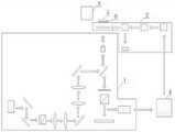
图1表示基于系综金刚石NV色心的宽场量子相机的结构示意图。Figure 1 shows a schematic diagram of the structure of a wide-field quantum camera based on an ensemble diamond NV color center.
图2表示光路与荧光系统的结构示意图。Fig. 2 shows a schematic diagram of the structure of the optical path and the fluorescent system.
图3表示微波系统的结构示意图。Figure 3 shows a schematic diagram of the structure of the microwave system.
图4表示待测芯片的部分示意图。Fig. 4 shows a partial schematic diagram of the chip to be tested.
图5表示磁场(Gs)分布检测成像的示意图。Fig. 5 shows a schematic diagram of magnetic field (Gs) distribution detection imaging.
图6表示温度(℃)分布检测成像的示意图。Fig. 6 shows a schematic diagram of temperature (°C) distribution detection imaging.
图中:1-光路与荧光系统,2-微波系统,3-外加磁场系统,4-采集控制与数据处理系统,5-待测芯片,6-系综金刚石,7-光源激光器,8a-反射镜组Ⅰ,8b-反射镜组Ⅱ,8c-反射镜组Ⅲ,9-二分之一波片,10-偏振分光棱镜,11a-平凸镜组Ⅰ,11b-平凸镜组Ⅱ,12-二向色镜,13-物镜,14-高通滤光片,15-50:50分光棱镜,16-CMOS相机,17-光电探测器,18-微波源,19-微波功率放大器,20-环形器,21-辐射天线,22-匹配电阻。In the figure: 1-optical path and fluorescence system, 2-microwave system, 3-applied magnetic field system, 4-acquisition control and data processing system, 5-chip to be tested, 6-ensemble diamond, 7-light source laser, 8a-reflection Mirror group I, 8b-mirror group II, 8c-mirror group III, 9-half wave plate, 10-polarization beam splitter, 11a-plano-convex mirror group I, 11b-plano-convex mirror group II, 12 -Dichroic mirror, 13-objective lens, 14-high-pass filter, 15-50:50 beam splitter, 16-CMOS camera, 17-photodetector, 18-microwave source, 19-microwave power amplifier, 20-ring device, 21-radiating antenna, 22-matching resistor.
具体实施方式Detailed ways
下面结合附图对本发明的具体实施例进行详细说明。Specific embodiments of the present invention will be described in detail below in conjunction with the accompanying drawings.
一种基于系综氮原子-空位色心的多物理参数宽场量子相机,该设备用于对待测芯片的磁场和温度进行成像。具体如图1所示,包括光路与荧光系统1、微波系统2、外加磁场系统3、采集控制与数据处理系统4和系综金刚石6。A multi-physics parameter wide-field quantum camera based on ensemble nitrogen atom-vacancy color center, which is used to image the magnetic field and temperature of the chip under test. Specifically as shown in FIG. 1 , it includes an optical path and
如图2所示,光路与荧光系统1包括光源激光器、反射镜组、二分之一波片9、偏振分光棱镜10、平凸镜组、二向色镜12、物镜13、高通滤光片14、50:50分光棱镜15、CMOS相机16、光电探测器17。光路与荧光系统具体分为共聚焦荧光激发收集系统和反射镜-透镜组。反射镜系统通过多对反射镜将激光反射到合适位置,并通过两对凸透镜组将其光斑放大到合适大小。As shown in Figure 2, the optical path and
如图2所示,光源激光器7发出的532nm连续激光通过反射镜组Ⅰ进行准直后进入用于实现激光偏振态的调节并且实现激光光强的调节的二分之一波片9和偏振分光棱镜10;之后激光通过平凸镜组Ⅰ11a进行光斑大小调节后再次通过反射镜组Ⅱ8b将激光通过平凸镜组Ⅱ11b进行光斑大小调节后通过反射镜组Ⅲ8c将激光以合适的角度和高度入射到共聚焦荧光激发收集系统中的二向色镜12。二向色镜12安装于荧光收集光路中,激光转向通过物镜13聚焦到系综金刚石6上;系综金刚石6处于外加磁场系统3提供的均匀偏置磁场内,系综金刚石6的NV色心发生激化并辐射出红色荧光,荧光被物镜13收集后通过二向色镜12滤掉绿色激光后先通过高通滤光片14,再通过50:50分光棱镜15分成两束分别进入CMOS相机16和光电探测器17;最后CMOS相机16采集到荧光变化的图像数据被采集控制与数据处理系统4处理成磁场分布和温度数据。As shown in Figure 2, the 532nm continuous laser light emitted by the
如图3所示,微波系统包括微波源18、微波功率放大器19、环形器20、辐射天线21和匹配电阻22。微波系统中的微波源18是采用外部脉冲信号控制微波的开关和步进时间,微波源18发出的微波信号输送到微波功率放大器19,功率放大后的微波信号之后进入环形器20,环形器20可以防止反射的微波信号返回,将返回的微波信号由匹配电阻22吸收,防止其干扰信号和仪器损坏。最后微波信号被输送到辐射天线21上,辐射天线再把微波能量馈送到系综金刚石6的NV色心。As shown in FIG. 3 , the microwave system includes a
系综金刚石6的NV色心是金刚石中的一种较为常见的、光学性质极好的缺陷,由一个氮取代碳原子和空位构成,空位周围有三个碳原子,NV色心的轴向,通常定义为氮原子和空位的连接轴向,具有C3V对称性。NV色心在波长532nm的绿色激光辐照下,被激发态返回基态时可辐射出红色荧光,其强度受多种因素的影响,包括磁场、温度、微波功率和频率等。The NV color center of ensemble diamond 6 is a relatively common defect in diamond with excellent optical properties. It is composed of a nitrogen-substituted carbon atom and a vacancy. There are three carbon atoms around the vacancy. The axial direction of the NV color center is usually Defined as the connection axis of nitrogen atoms and vacancies, it has C3V symmetry. Under the irradiation of green laser with a wavelength of 532nm, the NV color center can radiate red fluorescence when the excited state returns to the ground state, and its intensity is affected by many factors, including magnetic field, temperature, microwave power and frequency.
具体实施时,待测芯片5和系综金刚石6紧密贴合。During specific implementation, the chip 5 to be tested and the ensemble diamond 6 are closely attached.
外加磁场系统3的作用是实现磁场大小的调节,让不同NV轴方向的共振峰全部退简并,产生ODMR。ODMR,即光探测磁共振技术,基于光学检测的电子自旋共振技术,其原理是利用共聚焦显微镜来检测NV色心自旋依赖的荧光强度。外加磁场系统3为永磁体,永磁体由一对直径10mm、高20mm的圆柱形钕铁硼永磁铁组成,磁铁的磁化强度为1.2×10⁶Am-1。The function of the external
采集控制与数据处理系统4,即终端处理器-计算机,其作用是对采集到的图片数据进行数据处理,通过解算得到需要的探测结果。具体为,采集控制与数据处理系统通过Labview软件控制数据采集板卡实现相机曝光时间与微波源微波频率步进的同步,保证单张图对应单一微波频率;采集控制与数据处理系统通过CMOS相机控制软件保存采集到的图片,像素面积0.27mm×0.48mm;采集控制与数据处理系统通过Matlab软件,对采集到的图片数据利用三轴解算代码进行数据处理从而解算出需要的探测结果。The acquisition control and data processing system 4, namely the terminal processor-computer, is used to process the collected picture data and obtain the required detection results through calculation. Specifically, the acquisition control and data processing system controls the data acquisition board through Labview software to realize the synchronization of the camera exposure time and the microwave frequency step of the microwave source, ensuring that a single image corresponds to a single microwave frequency; the acquisition control and data processing system is controlled by a CMOS camera The software saves the collected pictures, with a pixel area of 0.27mm×0.48mm; the collection control and data processing system uses Matlab software to process the collected picture data using the three-axis calculation code to solve the required detection results.
光源激光器7发出的激光用于金刚石NV色心的光极化和光读出。激光波长为532nm,最大输出功率为150mW,功率稳定性优于1%,光束直径约0.7mm。光极化,即通过荧光强度达到最大值,来确保NV色心完全极化到0态。光读出,即通过荧光获得微波作用后的量子态信息。The laser light emitted by the
反射镜组Ⅰ8a包括两个反射镜,用于对连续激光进行准直。Mirror group I8a includes two mirrors for collimating continuous laser light.
二分之一波片9和偏振分光棱镜10,该组合可实现激光偏振态的调节同时还可以实现激光光强的调节。The combination of the half-
两组平凸镜(平凸镜组Ⅰ11a和平凸镜组Ⅱ11b)目的是实现光斑大小的调节。The purpose of two groups of plano-convex mirrors (plano-convex mirror group I11a and plano-convex mirror group II11b) is to adjust the spot size.
反射镜组Ⅱ8b和反射镜组Ⅲ8c,目的是调节位置和高度使激光入射到二向色镜。Mirror group II8b and mirror group III8c are used to adjust the position and height so that the laser light is incident on the dichroic mirror.
二向色镜12,其作用是把激光反射使得激光进入共聚焦光路中,从而照射到金刚石实现NV色心的极化和使物镜采集到的红色荧光通过而阻挡反射回来的绿色激光。The function of the
高通滤光片14透射波长大于650nm小于800nm,目的是滤掉绿光和周围环境的等杂散光。The high-
分光棱镜15,其作用是将荧光分成两束荧光并分别进入CMOS相机和光电探测器(PD)。
CMOS相机16,目的是采集图像个数,进行成像。The purpose of the
光电探测器(PD)17,作用是更快确定微波扫频范围和调节磁场方向。The photodetector (PD) 17 is used to more quickly determine the microwave frequency sweep range and adjust the direction of the magnetic field.
微波源18,属于信号发生器,利用其外部触发模式,实现外部脉冲信号控制微波的开和关。The
微波功率放大器19,可以实现对微波信号的功率放大。The
环形器20,其作用是防止反射的微波信号返回,将返回的微波信号由匹配电阻吸收,防止其干扰信号和仪器损坏。The function of the
匹配电阻22,其作用是吸收返回的微波信号。The matching
辐射天线21,其作用是把微波能量馈送到金刚石NV自旋上。The
系综金刚石6的尺寸不小于4mm×4mm×0.5mm、不大于5mm×5mm×0.5mm,含氮量不低于5%,直接宽场成像区域不低于9.5mm×5.5mm。The size of the ensemble diamond 6 is not less than 4mm×4mm×0.5mm, not more than 5mm×5mm×0.5mm, the nitrogen content is not less than 5%, and the direct wide-field imaging area is not less than 9.5mm×5.5mm.
具体应用时,基于系综金刚石NV色心的宽场量子相机用于对微型电加热芯片的测量如图4所示,视场内显示2条电流方向相反的微型芯片表面结构,单条导线宽度为0.07mm,两条导线间间距为0.03mm。磁场成像测试结果(如图5所示)和温度成像测试结果(如图6所示)表明该宽场量子相机实现多物理参数测试的可行性。In specific applications, the wide-field quantum camera based on the ensemble diamond NV color center is used to measure the micro-electric heating chip, as shown in Figure 4, the surface structure of two micro-chips with opposite current directions is displayed in the field of view, and the width of a single wire is 0.07mm, the distance between two wires is 0.03mm. The magnetic field imaging test results (as shown in Figure 5) and the temperature imaging test results (as shown in Figure 6) show the feasibility of the wide-field quantum camera for multi-physical parameter testing.
最后所应说明的是,以上实施例仅用以说明本发明的技术方案而非限制,尽管参照本发明实施例进行了详细说明,本领域的普通技术人员应当理解,对本发明的技术方案进行修改或者等同替换,都不脱离本发明的技术方案的精神和范围,其均应涵盖本发明的权利要求保护范围中。Finally, it should be noted that the above embodiments are only used to illustrate the technical solutions of the present invention rather than limit them. Although detailed descriptions have been made with reference to the embodiments of the present invention, those of ordinary skill in the art should understand that the technical solutions of the present invention are modified Or equivalent replacements do not deviate from the spirit and scope of the technical solutions of the present invention, and all of them should be included in the protection scope of the claims of the present invention.
Claims (2)
Priority Applications (1)
| Application Number | Priority Date | Filing Date | Title |
|---|---|---|---|
| CN202011585896.6ACN112683332B (en) | 2020-12-29 | 2020-12-29 | Multi-physical-parameter wide-field quantum camera based on ensemble nitrogen atom-vacancy color center |
Applications Claiming Priority (1)
| Application Number | Priority Date | Filing Date | Title |
|---|---|---|---|
| CN202011585896.6ACN112683332B (en) | 2020-12-29 | 2020-12-29 | Multi-physical-parameter wide-field quantum camera based on ensemble nitrogen atom-vacancy color center |
Publications (2)
| Publication Number | Publication Date |
|---|---|
| CN112683332A CN112683332A (en) | 2021-04-20 |
| CN112683332Btrue CN112683332B (en) | 2022-10-28 |
Family
ID=75453602
Family Applications (1)
| Application Number | Title | Priority Date | Filing Date |
|---|---|---|---|
| CN202011585896.6AActiveCN112683332B (en) | 2020-12-29 | 2020-12-29 | Multi-physical-parameter wide-field quantum camera based on ensemble nitrogen atom-vacancy color center |
Country Status (1)
| Country | Link |
|---|---|
| CN (1) | CN112683332B (en) |
Families Citing this family (15)
| Publication number | Priority date | Publication date | Assignee | Title |
|---|---|---|---|---|
| CN113640715B (en)* | 2021-08-18 | 2022-09-09 | 中国科学技术大学 | A kind of solid-state spin magnetic sensor and magnetic field measurement method |
| CN113834963A (en)* | 2021-09-06 | 2021-12-24 | 国仪量子(合肥)技术有限公司 | Current detection device and method based on NV color center sensor and storage medium |
| CN114113151B (en)* | 2021-11-08 | 2024-10-25 | 中国科学技术大学 | Coupled magnetic imaging device and measurement method |
| CN114047556B (en)* | 2021-11-15 | 2024-01-30 | 中国电子科技集团公司第十三研究所 | Magnetic force detecting head and magnetic force detecting system based on diamond NV color center |
| CN113933906B (en)* | 2021-11-15 | 2024-02-13 | 中国电子科技集团公司第十三研究所 | Diamond NV color center magnetic detection module and magnetic detection system |
| CN115128518B (en)* | 2022-06-24 | 2025-05-09 | 中北大学 | High-sensitivity differential magnetic acquisition system for NV color centers based on frequency-agile microwave modulation technology |
| CN115201169B (en)* | 2022-07-14 | 2025-02-07 | 山东大学 | A method and device for polarizing electron and nuclear spins in a single NV color center |
| CN115219965A (en)* | 2022-08-10 | 2022-10-21 | 南京邮电大学 | Wide-field-of-view rapid imaging measurement system and method based on diamond NV color center |
| CN115951279A (en)* | 2022-12-02 | 2023-04-11 | 哈尔滨工业大学 | Microwave coupling optical detection magnetic resonance device |
| CN115791740B (en)* | 2023-02-08 | 2023-05-09 | 安徽省国盛量子科技有限公司 | Microwave reflection imaging detection device and method based on diamond NV color center |
| CN117147004B (en)* | 2023-10-30 | 2024-03-26 | 之江实验室 | A high-precision temperature and magnetic field signal measurement device for weak magnetic field environments |
| CN117705932B (en)* | 2024-02-06 | 2024-04-23 | 高速铁路建造技术国家工程研究中心 | Quantum nondestructive sensor and rail surface defect detector |
| CN119000720B (en)* | 2024-10-25 | 2024-12-20 | 高速铁路建造技术国家工程研究中心 | Combined probe and quantum detection equipment |
| CN119511161A (en)* | 2024-11-18 | 2025-02-25 | 东南大学 | A microwave-free electromagnetic field measurement method and device based on NV color center |
| CN119714588B (en)* | 2024-12-24 | 2025-09-30 | 中国计量科学研究院 | Diamond nitrogen vacancy color center thermometer excitation laser stabilization control device and method |
Family Cites Families (13)
| Publication number | Priority date | Publication date | Assignee | Title |
|---|---|---|---|---|
| CN102291091B (en)* | 2011-06-16 | 2014-07-23 | 熊猫电子集团有限公司 | Linear microwave power amplifier |
| US9766181B2 (en)* | 2013-06-28 | 2017-09-19 | Massachusetts Institute Of Technology | Wide-field imaging using nitrogen vacancies |
| US9891297B2 (en)* | 2015-03-13 | 2018-02-13 | President And Fellows Of Harvard College | Magnetic sensing and imaging using interactions between surface electron spins and solid state spins |
| CN105444749B (en)* | 2015-11-07 | 2018-02-02 | 中北大学 | Cluster NV colour center diamond solid-state spin resonance gyroscopes based on Baily phase shift |
| US10394008B2 (en)* | 2016-10-19 | 2019-08-27 | Cornell University | Hyperspectral multiphoton microscope for biomedical applications |
| CN107356820A (en)* | 2017-06-07 | 2017-11-17 | 南京邮电大学 | A kind of electromagnetic field near field imaging system and method based on pulse optical detection magnetic resonance |
| CN109143121B (en)* | 2018-08-13 | 2021-05-04 | 南京昆腾科技有限公司 | Microwave field quantitative test system and method based on pulse modulation |
| CN111830073B (en)* | 2019-04-22 | 2022-10-28 | 中国科学技术大学 | High-throughput single-molecule magnetic resonance measurement device and measurement method |
| CN110554068A (en)* | 2019-09-11 | 2019-12-10 | 吉林大学 | Experimental device for detecting ODMR spectrum of diamond NV color center based on DAC device |
| CN111031622B (en)* | 2019-12-30 | 2022-02-25 | 广东美的厨房电器制造有限公司 | Microwave heating assembly, microwave heating equipment and control method |
| CN111239653B (en)* | 2020-02-10 | 2025-05-16 | 致真精密仪器(青岛)有限公司 | Magnetic imaging device and imaging method based on diamond NV color center and Kerr effect |
| CN111398231B (en)* | 2020-03-26 | 2022-02-01 | 西安交通大学 | Scanning detection system based on diamond NV color center |
| CN111474158B (en)* | 2020-05-20 | 2021-10-01 | 中国科学技术大学 | A two-dimensional spectral imaging system and two-dimensional imaging method |
- 2020
- 2020-12-29CNCN202011585896.6Apatent/CN112683332B/enactiveActive
Also Published As
| Publication number | Publication date |
|---|---|
| CN112683332A (en) | 2021-04-20 |
Similar Documents
| Publication | Publication Date | Title |
|---|---|---|
| CN112683332B (en) | Multi-physical-parameter wide-field quantum camera based on ensemble nitrogen atom-vacancy color center | |
| CN111830073B (en) | High-throughput single-molecule magnetic resonance measurement device and measurement method | |
| CN103439254B (en) | A kind of point pupil confocal laser Raman spectra test method and device | |
| CN103969239B (en) | A kind of point pupil laser differential confocal Raman spectra test method and device | |
| CN103163106B (en) | Super-resolution fluorescent lifetime imaging method and device based on stimulated emission lost | |
| CN112083364B (en) | Microwave field and temperature field array type quantitative test system and method | |
| CN107192702B (en) | Spectroscopic pupil laser confocal CARS (coherent anti-Raman scattering) microspectroscopy testing method and device | |
| CN104634766B (en) | Super-resolution device and method based on pumping-probe technology | |
| EP2769417A1 (en) | Systems and methods for deterministic emitter switch microscopy | |
| CN114858314B (en) | Diamond stress measurement system and method based on NV color center | |
| CN106990095B (en) | Reflection-type confocal CARS micro-spectrometer method and apparatus | |
| CN111024659B (en) | A method and device for multi-image reconstruction microscopy based on parallel detection | |
| CN113219387A (en) | Solid-state quantum spin fluorescence imaging system | |
| CN118443630B (en) | A device for removing background noise based on frequency domain modulation | |
| CN117705831B (en) | A quantum sensor and nondestructive testing method based on microwave reflection | |
| CN103940799A (en) | Laser dual-axis confocal Brillouin-Raman spectral measurement method and apparatus | |
| CN114415081B (en) | Device based on ensemble nitrogen-vacancy color center | |
| CN113777540A (en) | Diamond NV color center magnetometer containing magnetic flux collector | |
| CN117783070B (en) | Fluorescent signal coding super-resolution microscopic imaging method | |
| CN107167456A (en) | Transmission-type differential confocal CARS micro-spectrometer method and devices | |
| WO2024087614A1 (en) | Ratiometric fluorescence emission super-resolution imaging method | |
| CN115032224B (en) | Pulsed high field magnetic resonance system | |
| CN107167457A (en) | The confocal CARS micro-spectrometers method and device of transmission-type | |
| CN119199674A (en) | Quantum detection system and detection method | |
| CN110596630B (en) | Frequency calibration system and method based on diamond NV color center quantum precision measurement device |
Legal Events
| Date | Code | Title | Description |
|---|---|---|---|
| PB01 | Publication | ||
| PB01 | Publication | ||
| SE01 | Entry into force of request for substantive examination | ||
| SE01 | Entry into force of request for substantive examination | ||
| GR01 | Patent grant | ||
| GR01 | Patent grant |