Movatterモバイル変換


[0]ホーム

URL:


CN112669761B - Display panel, manufacturing method thereof, and display device - Google Patents

Display panel, manufacturing method thereof, and display device
Download PDF

Info

Publication number
CN112669761B
CN112669761BCN202011386324.5ACN202011386324ACN112669761BCN 112669761 BCN112669761 BCN 112669761BCN 202011386324 ACN202011386324 ACN 202011386324ACN 112669761 BCN112669761 BCN 112669761B
Authority
CN
China
Prior art keywords
pulse width
width modulation
led
unit
electrically connected
Prior art date
Legal status (The legal status is an assumption and is not a legal conclusion. Google has not performed a legal analysis and makes no representation as to the accuracy of the status listed.)
Active
Application number
CN202011386324.5A
Other languages
Chinese (zh)
Other versions
CN112669761A (en
Inventor
邢亮
Current Assignee (The listed assignees may be inaccurate. Google has not performed a legal analysis and makes no representation or warranty as to the accuracy of the list.)
Xiamen Tianma Microelectronics Co Ltd
Original Assignee
Xiamen Tianma Microelectronics Co Ltd
Priority date (The priority date is an assumption and is not a legal conclusion. Google has not performed a legal analysis and makes no representation as to the accuracy of the date listed.)
Filing date
Publication date
Application filed by Xiamen Tianma Microelectronics Co LtdfiledCriticalXiamen Tianma Microelectronics Co Ltd
Priority to CN202011386324.5ApriorityCriticalpatent/CN112669761B/en
Priority to US17/159,777prioritypatent/US12087747B2/en
Publication of CN112669761ApublicationCriticalpatent/CN112669761A/en
Application grantedgrantedCritical
Publication of CN112669761BpublicationCriticalpatent/CN112669761B/en
Activelegal-statusCriticalCurrent
Anticipated expirationlegal-statusCritical

Links

Images

Classifications

Landscapes

Abstract

Translated fromChinese

本发明公开了一种显示面板及其制备方法、显示装置。其中,显示面板包括:衬底、位于显示区的LED阵列以及位于显示区的脉宽调制芯片阵列,LED阵列包括阵列排布的多个LED单元,脉宽调制芯片阵列包括阵列排布的多个脉宽调制芯片,多个LED单元与多个脉宽调制芯片一一对应电连接,脉宽调制芯片用于调节与之电连接的LED单元的发光时长。本发明实施例提供的显示面板,通过在显示区设置脉宽调制芯片与LED单元一一对应连接,使得脉宽调制芯片和与之电连接的LED单元之间的距离较近,从而降低信号延迟,并且不同脉宽调制芯片和与其对应的LED单元之间的距离相同或相当,减少不同位置处LED单元的信号差异,提高了显示面板的亮度均一性。

Figure 202011386324

The invention discloses a display panel, a preparation method thereof, and a display device. Among them, the display panel includes: a substrate, an LED array located in the display area, and a pulse width modulation chip array located in the display area. The LED array includes a plurality of LED units arranged in an array, and the pulse width modulation chip array includes a plurality of LED units arranged in an array. A pulse width modulation chip, a plurality of LED units and a plurality of pulse width modulation chips are electrically connected one by one, and the pulse width modulation chip is used to adjust the light-emitting duration of the LED units electrically connected to it. In the display panel provided by the embodiment of the present invention, the pulse width modulation chip and the LED unit are connected in one-to-one correspondence in the display area, so that the distance between the pulse width modulation chip and the LED unit electrically connected to it is relatively close, thereby reducing the signal delay , and the distances between different pulse width modulation chips and their corresponding LED units are the same or equivalent, reducing signal differences of LED units at different positions and improving the brightness uniformity of the display panel.

Figure 202011386324

Description

Translated fromChinese
一种显示面板及其制备方法、显示装置Display panel, manufacturing method thereof, and display device

技术领域technical field

本发明实施例涉及显示技术领域,尤其涉及一种显示面板及其制备方法、 显示装置。Embodiments of the present invention relate to the field of display technology, and in particular to a display panel, a manufacturing method thereof, and a display device.

背景技术Background technique

随着发光技术和显示技术的不断发展,以Mini LED和Micro LED为主流的 微小型发光二极管显示屏,由于其亮度高、对比度高、解析度高以及色彩饱和 度高等优势,逐渐成为各厂商关注的重点。With the continuous development of light-emitting technology and display technology, miniature light-emitting diode displays, with Mini LED and Micro LED as the mainstream, have gradually become the focus of various manufacturers due to their advantages of high brightness, high contrast, high resolution and high color saturation. the key of.

目前,Mini LED和Micro LED显示屏等显示装置或发光装置,由数量众多 的小尺寸发光二极管(Light Emitting Diode,LED)阵列组成,驱动发光二极管 发光的驱动IC通常设置在显示面板的周边,发光二极管通过走线与驱动IC电 连接,由于走线自身存在阻抗,随着走线长度的增加,距离驱动IC较远的发光 二极管会发生信号延迟,使得驱动IC远端和近端的发光二极管接收到的信号产 生差异,导致显示亮度均一性较差。At present, display devices or light-emitting devices such as Mini LED and Micro LED displays are composed of a large number of small-sized light-emitting diode (Light Emitting Diode, LED) arrays, and the driver IC that drives the light-emitting diodes to emit light is usually arranged around the display panel to emit light. The diode is electrically connected to the driver IC through a wire. Due to the impedance of the wire itself, as the length of the wire increases, the signal delay of the light-emitting diode far from the driver IC will occur, so that the light-emitting diodes at the far end and the near end of the driver IC receive The difference in the received signal results in poor uniformity of display brightness.

发明内容Contents of the invention

本发明提供一种显示面板及其制备方法、显示装置,以提高显示亮度均一 性。The invention provides a display panel, a preparation method thereof, and a display device, so as to improve the uniformity of display brightness.

第一方面,本发明实施例提供了一种显示面板,包括:In a first aspect, an embodiment of the present invention provides a display panel, including:

衬底,所述衬底包括显示区;a substrate comprising a display region;

位于所述显示区的LED阵列;所述LED阵列包括阵列排布的多个LED单元;An LED array located in the display area; the LED array includes a plurality of LED units arranged in an array;

位于所述显示区的脉宽调制芯片阵列;所述脉宽调制芯片阵列包括阵列排 布的多个脉宽调制芯片;A pulse width modulation chip array located in the display area; the pulse width modulation chip array includes a plurality of pulse width modulation chips arranged in an array;

多个所述LED单元与多个所述脉宽调制芯片一一对应电连接;所述脉宽调 制芯片用于调节与之电连接的所述LED单元的发光时长。A plurality of the LED units are electrically connected to a plurality of the pulse width modulation chips in one-to-one correspondence; the pulse width modulation chips are used to adjust the light-emitting duration of the LED units electrically connected thereto.

第二方面,本发明实施例还提供了一种显示装置,包括第一方面所述的显 示面板。In the second aspect, the embodiment of the present invention also provides a display device, including the display panel described in the first aspect.

第三方面,本发明实施例还提供了一种显示面板的制备方法,该制备方法 包括:In a third aspect, the embodiment of the present invention also provides a method for preparing a display panel, the method comprising:

提供一衬底;所述衬底包括显示区;A substrate is provided; the substrate includes a display area;

在所述衬底的显示区设置LED阵列以及脉宽调制芯片阵列;An LED array and a pulse width modulation chip array are arranged in the display area of the substrate;

其中,所述LED阵列包括阵列排布的多个LED单元;所述脉宽调制芯片阵 列包括阵列排布的多个脉宽调制芯片;多个所述LED单元与多个所述脉宽调制 芯片一一对应电连接;所述脉宽调制芯片用于调节与之电连接的所述LED单元 的发光时长。Wherein, the LED array includes a plurality of LED units arranged in an array; the pulse width modulation chip array includes a plurality of pulse width modulation chips arranged in an array; a plurality of the LED units and a plurality of the pulse width modulation Chips are electrically connected one by one; the pulse width modulation chip is used to adjust the light-emitting duration of the LED unit electrically connected to it.

本发明实施例提供的显示面板,通过在显示区设置脉宽调制芯片与LED单 元一一对应连接,并通过脉宽调制芯片调节与之电连接的LED单元的发光时长 来控制LED单元的显示灰阶,使得脉宽调制芯片和与之电连接的LED单元之间的距离较近,从而降低信号延迟,并且不同脉宽调制芯片和与其对应的LED单 元之间的距离相同或相当,减少不同位置处LED单元的信号差异,提高显示面 板的亮度均一性。The display panel provided by the embodiment of the present invention controls the display of the LED unit by setting a pulse width modulation chip in the display area and connecting the LED units in one-to-one correspondence, and adjusting the light-emitting duration of the LED unit electrically connected to the pulse width modulation chip. Grayscale, so that the distance between the PWM chip and the LED unit electrically connected to it is relatively close, thereby reducing the signal delay, and the distance between different PWM chips and the corresponding LED unit is the same or equivalent, reducing The signal difference of LED units at different positions improves the brightness uniformity of the display panel.

附图说明Description of drawings

图1为本发明实施例提供的一种显示面板的结构示意图;FIG. 1 is a schematic structural diagram of a display panel provided by an embodiment of the present invention;

图2为图1沿A-A’方向的剖面结构示意图;Fig. 2 is the schematic cross-sectional structure diagram of Fig. 1 along A-A ' direction;

图3为本发明实施例提供的另一种显示面板的结构示意图;FIG. 3 is a schematic structural diagram of another display panel provided by an embodiment of the present invention;

图4为图3沿B-B’方向的剖面结构示意图;Fig. 4 is the sectional structure schematic diagram along B-B ' direction of Fig. 3;

图5为本发明实施例提供的又一种显示面板的结构示意图;FIG. 5 is a schematic structural diagram of another display panel provided by an embodiment of the present invention;

图6为本发明实施例提供的一种显示面板的第一侧的结构示意图;FIG. 6 is a schematic structural diagram of a first side of a display panel provided by an embodiment of the present invention;

图7为本发明实施例提供的一种显示面板的第二侧的结构示意图;FIG. 7 is a schematic structural diagram of a second side of a display panel provided by an embodiment of the present invention;

图8为本发明实施例提供的一种脉宽调制芯片的结构示意图;FIG. 8 is a schematic structural diagram of a pulse width modulation chip provided by an embodiment of the present invention;

图9为本发明实施例提供的另一种脉宽调制芯片的结构示意图;FIG. 9 is a schematic structural diagram of another pulse width modulation chip provided by an embodiment of the present invention;

图10为本发明实施例提供的一种显示面板的局部剖面结构示意图;FIG. 10 is a partial cross-sectional structural schematic diagram of a display panel provided by an embodiment of the present invention;

图11为本发明实施例提供的又一种脉宽调制芯片的结构示意图;FIG. 11 is a schematic structural diagram of another pulse width modulation chip provided by an embodiment of the present invention;

图12为本发明实施例提供的又一种脉宽调制芯片的结构示意图;FIG. 12 is a schematic structural diagram of another pulse width modulation chip provided by an embodiment of the present invention;

图13为本发明实施例提供的另一种显示面板的局部剖面结构示意图;FIG. 13 is a partial cross-sectional structural schematic diagram of another display panel provided by an embodiment of the present invention;

图14为本发明实施例提供的又一种显示面板的局部剖面结构示意图;FIG. 14 is a partial cross-sectional structural schematic diagram of another display panel provided by an embodiment of the present invention;

图15为本发明实施例提供的又一种脉宽调制芯片的结构示意图;FIG. 15 is a schematic structural diagram of another pulse width modulation chip provided by an embodiment of the present invention;

图16为本发明实施例提供的一种脉宽调制芯片的工作流程示意图;FIG. 16 is a schematic diagram of a workflow of a pulse width modulation chip provided by an embodiment of the present invention;

图17为本发明实施例提供的又一种显示面板的结构示意图;FIG. 17 is a schematic structural diagram of another display panel provided by an embodiment of the present invention;

图18为本发明实施例提供的另一种显示面板的第一侧的结构示意图;FIG. 18 is a schematic structural diagram of the first side of another display panel provided by an embodiment of the present invention;

图19为本发明实施例提供的另一种显示面板的第二侧的结构示意图;FIG. 19 is a schematic structural diagram of the second side of another display panel provided by an embodiment of the present invention;

图20为本发明实施例提供的又一种显示面板的局部剖面结构示意图;FIG. 20 is a partial cross-sectional structural schematic diagram of another display panel provided by an embodiment of the present invention;

图21为本发明实施例提供的又一种显示面板的局部剖面结构示意图;Fig. 21 is a partial cross-sectional structural schematic diagram of another display panel provided by an embodiment of the present invention;

图22为本发明实施例提供的又一种显示面板的结构示意图;Fig. 22 is a schematic structural diagram of another display panel provided by an embodiment of the present invention;

图23为本发明实施例提供的又一种显示面板的第一侧的结构示意图;Fig. 23 is a schematic structural diagram of the first side of another display panel provided by an embodiment of the present invention;

图24为本发明实施例提供的又一种显示面板的第二侧的结构示意图;Fig. 24 is a schematic structural diagram of the second side of another display panel provided by an embodiment of the present invention;

图25为本发明实施例提供的一种显示面板的局部结构示意图;FIG. 25 is a schematic diagram of a partial structure of a display panel provided by an embodiment of the present invention;

图26为本发明实施例提供的另一种显示面板的局部结构示意图;Fig. 26 is a partial structural schematic diagram of another display panel provided by an embodiment of the present invention;

图27为本发明实施例提供的又一种显示面板的局部结构示意图;Fig. 27 is a partial structural schematic diagram of another display panel provided by an embodiment of the present invention;

图28为本发明实施例提供的又一种显示面板的局部结构示意图;FIG. 28 is a schematic diagram of a partial structure of another display panel provided by an embodiment of the present invention;

图29为本发明实施例提供的又一种显示面板的局部结构示意图;FIG. 29 is a schematic diagram of a partial structure of another display panel provided by an embodiment of the present invention;

图30为本发明实施例提供的一种显示装置的结构示意图;FIG. 30 is a schematic structural diagram of a display device provided by an embodiment of the present invention;

图31为本发明实施例提供的一种显示面板的制备方法的流程示意图;FIG. 31 is a schematic flowchart of a method for manufacturing a display panel provided by an embodiment of the present invention;

图32为本发明实施例提供的另一种显示面板的制备方法的流程示意图。FIG. 32 is a schematic flowchart of another method for manufacturing a display panel provided by an embodiment of the present invention.

具体实施方式Detailed ways

下面结合附图和实施例对本发明作进一步的详细说明。可以理解的是,此 处所描述的具体实施例仅仅用于解释本发明,而非对本发明的限定。另外还需 要说明的是,为了便于描述,附图中仅示出了与本发明相关的部分而非全部结 构。The present invention will be further described in detail below in conjunction with the accompanying drawings and embodiments. It can be understood that the specific embodiments described here are only used to explain the present invention, rather than to limit the present invention. In addition, it should be noted that, for the convenience of description, only parts relevant to the present invention are shown in the drawings but not all structures.

本发明实施例提供一种显示面板,该显示面板包括衬底,衬底包括显示区; 显示面板还包括位于显示区的LED阵列,LED阵列包括阵列排布的多个LED单 元;显示面板还包括位于显示区的脉宽调制芯片阵列,脉宽调制芯片阵列包括 阵列排布的多个脉宽调制芯片,多个LED单元与多个脉宽调制芯片一一对应电连接,脉宽调制芯片用于调节与之电连接的LED单元的发光时长。An embodiment of the present invention provides a display panel, the display panel includes a substrate, the substrate includes a display area; the display panel also includes an LED array located in the display area, and the LED array includes a plurality of LED units arranged in an array; the display panel also includes It includes a pulse width modulation chip array located in the display area. The pulse width modulation chip array includes multiple pulse width modulation chips arranged in an array. Multiple LED units are electrically connected to multiple pulse width modulation chips one by one. It is used to adjust the light-emitting duration of the LED unit electrically connected to it.

采用上述技术方案,通过在显示区设置脉宽调制芯片与LED单元一一对应 连接,并通过脉宽调制芯片调节与之电连接的LED单元的发光时长来控制LED 单元的显示灰阶,使得脉宽调制芯片和与之电连接的LED单元之间的距离较近,从而降低信号延迟,并且不同脉宽调制芯片和与其对应的LED单元之间的距离 相同或相当,减少不同位置处LED单元的信号差异,提高显示面板的亮度均一 性。Using the above technical scheme, by setting the pulse width modulation chip in the display area and connecting the LED units one by one, and adjusting the light-emitting time of the LED unit electrically connected to it through the pulse width modulation chip to control the display gray scale of the LED unit, so that the pulse The distance between the width modulation chip and the LED unit electrically connected to it is relatively close, thereby reducing the signal delay, and the distance between different pulse width modulation chips and the corresponding LED unit is the same or equivalent, reducing the distance between the LED units at different positions. Signal difference, improve the brightness uniformity of the display panel.

以上是本发明的核心思想,下面将结合本发明实施例中的附图,对本发明 实施例中的技术方案进行清楚、完整地描述。基于本发明中的实施例,本领域 普通技术人员在没有做出创造性劳动前提下,所获得的所有其他实施例,都属 于本发明保护的范围。The above is the core idea of the present invention, and the technical solutions in the embodiments of the present invention will be clearly and completely described below in conjunction with the accompanying drawings in the embodiments of the present invention. Based on the embodiments of the present invention, all other embodiments obtained by persons of ordinary skill in the art without making creative efforts belong to the protection scope of the present invention.

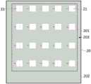
图1为本发明实施例提供的一种显示面板的结构示意图,图2为图1沿A-A’ 方向的剖面结构示意图,如图1和图2所示,本发明实施例提供的显示面板包 括衬底20,衬底20包括显示区201;该显示面板还包括位于显示区201的LED 阵列,LED阵列包括阵列排布的多个LED单元21;显示面板还包括位于显示区 201的脉宽调制芯片阵列,脉宽调制芯片阵列包括阵列排布的多个脉宽调制芯 片22。多个LED单元21与多个脉宽调制芯片22一一对应电连接,脉宽调制芯片22用于调节与之电连接的LED单元21的发光时长。Figure 1 is a schematic structural view of a display panel provided by an embodiment of the present invention, and Figure 2 is a schematic cross-sectional structural view of Figure 1 along the A-A' direction, as shown in Figure 1 and Figure 2, the display panel provided by an embodiment of the present invention Including asubstrate 20, thesubstrate 20 includes adisplay area 201; the display panel also includes an LED array located in thedisplay area 201, and the LED array includes a plurality ofLED units 21 arranged in an array; the display panel also includes an LED array located in thedisplay area 201 The width modulation chip array, the pulse width modulation chip array includes a plurality of pulsewidth modulation chips 22 arranged in an array.Multiple LED units 21 are electrically connected to multiple pulsewidth modulation chips 22 in one-to-one correspondence, and the pulsewidth modulation chips 22 are used to adjust the light-emitting duration of theLED units 21 electrically connected thereto.

其中,LED单元21可包括无机发光二极管,无机发光二极管可包括Mini-LED 和Micro-LED。Mini-LED是指单颗LED的尺寸在几百微米(μm)级的LED, Micro-LED是指单颗LED的尺寸小于一百微米(μm)的LED,Mini-LED和 Micro-LED均具有高解析度、高亮度、超省电、响应速度快、出光效率高和高 寿命等优点。在其他实施例中,LED单元21也可采用其他类型的LED,且LED 单元21可以为正装芯片结构、倒装芯片结构或者垂直封装结构,本领域技术人 员可根据实际需求进行设置,本发明实施例对此不作限定。Wherein, theLED unit 21 may include inorganic light emitting diodes, and the inorganic light emitting diodes may include Mini-LEDs and Micro-LEDs. Mini-LED refers to LEDs with a single LED size of several hundred microns (μm), and Micro-LED refers to LEDs with a single LED size smaller than 100 microns (μm). Both Mini-LEDs and Micro-LEDs have It has the advantages of high resolution, high brightness, super power saving, fast response, high light extraction efficiency and long life. In other embodiments, theLED unit 21 can also use other types of LEDs, and theLED unit 21 can be a front-mounted chip structure, a flip-chip structure or a vertical packaging structure, and those skilled in the art can set it according to actual needs. The present invention The embodiment does not limit this.

继续参考图1和图2,每个LED单元21对应连接一个脉宽调制芯片22,脉 宽调制芯片22用于调节与之电连接的LED单元21的发光时长,进而通过调节 LED单元21的发光时长来控制LED单元21的显示灰阶。其中,LED单元21和脉宽调制芯片22可设置在衬底20的同一侧,也可设置在衬底20的不同侧。Continuing to refer to Fig. 1 and Fig. 2, eachLED unit 21 is correspondingly connected to a pulsewidth modulation chip 22, and the pulsewidth modulation chip 22 is used to adjust the light-emitting duration of theLED unit 21 electrically connected to it, and then by adjusting the light-emitting time of theLED unit 21 The display gray scale of theLED unit 21 is controlled by the time length. Wherein, theLED unit 21 and the pulsewidth modulation chip 22 can be arranged on the same side of thesubstrate 20 or on different sides of thesubstrate 20 .

示例性的,如图1和图2所示,本发明实施例以LED单元21和脉宽调制芯 片22可设置在衬底20的同一侧为例,脉宽调制芯片22位于显示区201,并与 LED单元21一一对应设置。相比于现有技术中通过设置在非显示区的驱动芯片 与显示区的各个LED单元连接,本发明实施例中脉宽调制芯片22和与之电连接 的LED单元21之间的距离较近,可降低信号延迟,并且不同脉宽调制芯片22 和与其对应的LED单元21之间的距离相同或相当,从而可减少不同位置处LED 单元21的信号差异,有利于提高显示面板的亮度均一性。Exemplarily, as shown in FIG. 1 and FIG. 2, the embodiment of the present invention takes theLED unit 21 and the pulsewidth modulation chip 22 as an example that can be arranged on the same side of thesubstrate 20, and the pulsewidth modulation chip 22 is located in thedisplay area 201, And set withLED unit 21 one-to-one correspondence. Compared with the prior art, the driver chip arranged in the non-display area is connected to each LED unit in the display area, the distance between the pulsewidth modulation chip 22 and theLED unit 21 electrically connected to it in the embodiment of the present invention is relatively short , can reduce the signal delay, and the distance between different pulsewidth modulation chips 22 and theircorresponding LED units 21 is the same or equivalent, thereby reducing the signal difference ofLED units 21 at different positions, which is conducive to improving the brightness uniformity of the display panel .

需要注意的是,显示面板可以单独采用调节LED单元21发光时长的方式来 实现不同灰阶的显示,在其他实施例中,还可在脉宽调制芯片22调节与之电连 接的LED单元21的发光时长的同时,结合调节LED单元21的驱动电流大小共 同实现不同灰阶的显示,本发明实施例对此不作限定。It should be noted that the display panel can realize the display of different gray scales by adjusting the light-emitting time of theLED unit 21 alone. In other embodiments, the pulsewidth modulation chip 22 can also adjust theLED unit 21 electrically connected to it. While adjusting the driving current of theLED unit 21, the display of different gray scales can be realized, which is not limited in the embodiment of the present invention.

本发明实施例提供的显示面板,通过在显示区201设置脉宽调制芯片22与 LED单元21一一对应连接,通过脉宽调制芯片22调节与之电连接的LED单元 21的发光时长来控制LED单元21的显示灰阶,使得脉宽调制芯片22和与之电 连接的LED单元21之间的距离较近,从而降低信号延迟,并且不同脉宽调制芯 片22和与其对应的LED单元21之间的距离相同或相当,减少不同位置处LED 单元21的信号差异,提高显示面板的亮度均一性。In the display panel provided by the embodiment of the present invention, by setting the pulsewidth modulation chip 22 in thedisplay area 201 to connect with theLED unit 21 in one-to-one correspondence, the LED is controlled by adjusting the light-emitting duration of theLED unit 21 electrically connected to the pulsewidth modulation chip 22. The display gray scale of theunit 21 makes the distance between the pulsewidth modulation chip 22 and theLED unit 21 electrically connected to it closer, thereby reducing the signal delay, and the difference between the pulsewidth modulation chip 22 and thecorresponding LED unit 21 The distance between them is the same or equivalent, reducing the signal difference of theLED unit 21 at different positions, and improving the brightness uniformity of the display panel.

可选的,各LED单元21的驱动电流的电流值相同。Optionally, the current value of the driving current of eachLED unit 21 is the same.

本发明实施例中LED单元实现不同灰阶的显示的方式可以是调节LED单元 21的发光时长,也可以是调节LED单元21的驱动电流大小。可选的,本发明 实施例还可以设置LED单元21的驱动电流的电流值相同,仅通过调节LED单元 21的发光时长来实现不同灰阶的显示的方式。In the embodiment of the present invention, the way that the LED unit realizes the display of different gray scales can be to adjust the light-emitting duration of theLED unit 21, or to adjust the driving current of theLED unit 21. Optionally, in the embodiment of the present invention, the current value of the driving current of theLED unit 21 can also be set to be the same, and only by adjusting the light-emitting duration of theLED unit 21 to realize the display mode of different gray scales.

具体的,由于LED单元在不同驱动电流下的发光效率差别很大,LED单元 工作在大电流时发光效率较高,工作在小电流时发光效率较低,这样在低灰阶 范围内,LED单元的驱动电流较小,使得在低灰阶范围内,LED单元发光效率 很低,因此会影响显示面板的稳定性。据此,本发明实施例设置各LED单元21 的驱动电流的电流值相同,通过调节LED单元21的发光时长来控制显示灰阶, 而非现有技术中的通过控制驱动电流大小来控制显示灰阶,使得流过LED单元 21的驱动电流大小始终相同,进而可以充分利用LED单元21大电流时高发光 效率的特性,使得在包括低灰阶范围的任意灰阶内,LED单元21的发光效率都 较高,提高LED单元21的发光效率,并确保显示面板的稳定性。Specifically, because the luminous efficiency of the LED unit varies greatly under different driving currents, the luminous efficiency of the LED unit is higher when it works at a high current, and the luminous efficiency is lower when it works at a low current. In this way, in the low gray scale range, the LED unit The driving current is small, so that in the low gray scale range, the luminous efficiency of the LED unit is very low, which will affect the stability of the display panel. Accordingly, in the embodiment of the present invention, the current value of the drive current of eachLED unit 21 is set to be the same, and the display gray scale is controlled by adjusting the light-emitting duration of theLED unit 21, instead of controlling the display gray scale by controlling the drive current in the prior art. steps, so that the magnitude of the driving current flowing through theLED unit 21 is always the same, and then the characteristics of high luminous efficiency of theLED unit 21 can be fully utilized when the current is high, so that the luminous efficiency of theLED unit 21 can be reduced in any gray scale including the low gray scale range. are higher, improve the luminous efficiency of theLED unit 21, and ensure the stability of the display panel.

继续参考图1,可选的,衬底20还包括非显示区202,显示面板还包括位 于非显示区202的驱动芯片23,多条数据线24和多条扫描线25。驱动芯片23 用于通过扫描线25向脉宽调制芯片22提供扫描信号,驱动芯片23用于通过数 据线24向脉宽调制芯片22提供数据信号。Continuing to refer to FIG. 1 , optionally, thesubstrate 20 further includes anon-display area 202, and the display panel further includes adriver chip 23 located in thenon-display area 202, a plurality ofdata lines 24 and a plurality ofscan lines 25. Thedriver chip 23 is used to provide scanning signals to the pulsewidth modulation chip 22 through thescan lines 25, and thedriver chip 23 is used to provide data signals to the pulsewidth modulation chip 22 through the data lines 24.

具体的,衬底20还包括非显示区202,非显示区202与显示区201相邻, 非显示区202设置有驱动芯片23,驱动芯片23通过扫描线25与脉宽调制芯片 22电连接,从而为脉宽调制芯片22提供扫描信号,驱动芯片23通过数据线24与脉宽调制芯片22电连接,从而为脉宽调制芯片22提供数据信号。其中,数 据信号与显示灰阶对应,脉宽调制芯片22接收到扫描信号时,根据数据信号产 生对应的脉宽调制(Pulse Width Modulation,PWM)信号,进而控制LED单元 21的发光时长,从而实现相应的灰阶显示。Specifically, thesubstrate 20 also includes anon-display area 202, thenon-display area 202 is adjacent to thedisplay area 201, thenon-display area 202 is provided with adriver chip 23, and thedriver chip 23 is electrically connected to the pulsewidth modulation chip 22 through thescan line 25, Thus, scan signals are provided for the pulsewidth modulation chip 22 , and thedriving chip 23 is electrically connected to the pulsewidth modulation chip 22 through thedata line 24 , thereby providing data signals for the pulsewidth modulation chip 22 . Wherein, the data signal corresponds to the display gray scale, and when the pulsewidth modulation chip 22 receives the scanning signal, it generates a corresponding pulse width modulation (Pulse Width Modulation, PWM) signal according to the data signal, and then controls the light-emitting duration of theLED unit 21, In this way, a corresponding gray scale display is realized.

需要注意的是,扫描信号和数据信号可由一个驱动芯片23提供,如图1所 示,采用一个驱动芯片23提供可减小驱动芯片23的占用空间,有助于提高屏 占比。在其他实施例中,扫描信号和数据信号也可由不同的驱动芯片23提供, 采用至少两个驱动芯片23时,各个驱动芯片23可设置于显示区201的同一侧, 也可分别设置在显示区201的不同侧,本发明实施例对此不作限定。It should be noted that the scan signal and the data signal can be provided by adriver chip 23, as shown in Figure 1, using adriver chip 23 to provide can reduce the occupied space of thedriver chip 23, which helps to increase the screen ratio. In other embodiments, the scan signal and the data signal can also be provided bydifferent driver chips 23. When at least twodriver chips 23 are used, eachdriver chip 23 can be arranged on the same side of thedisplay area 201, or can be arranged separately in the display area. The different sides of 201 are not limited in this embodiment of the present invention.

图3为本发明实施例提供的另一种显示面板的结构示意图,图4为图3沿 B-B’方向的剖面结构示意图,如图3和图4所示,可选的,衬底20包括相对 的第一侧203和第二侧204,LED阵列位于第一侧203,脉宽调制芯片阵列位于 第二侧204,衬底20采用透明材料。Fig. 3 is a schematic structural diagram of another display panel provided by an embodiment of the present invention, and Fig. 4 is a schematic cross-sectional structural diagram of Fig. 3 along the BB' direction, as shown in Fig. 3 and Fig. 4, optionally, asubstrate 20 Including the oppositefirst side 203 andsecond side 204, the LED array is located on thefirst side 203, the pulse width modulation chip array is located on thesecond side 204, and thesubstrate 20 is made of a transparent material.

其中,本发明实施例提供的显示面板衬底20采用透明材料,可应用于透明 显示中。如图3和图4所示,LED阵列和脉宽调制芯片阵列设置在衬底20的不 同侧,与LED阵列和脉宽调制芯片阵列均位于衬底20的同一侧相比,有助于降 低LED阵列和脉宽调制芯片阵列遮挡衬底20的面积,提高显示面板的透过率, 实现透明显示。Wherein, thedisplay panel substrate 20 provided by the embodiment of the present invention is made of a transparent material, which can be applied to a transparent display. As shown in Figures 3 and 4, the LED array and the pulse width modulation chip array are arranged on different sides of thesubstrate 20, compared with the LED array and the pulse width modulation chip array being all located on the same side of thesubstrate 20, it helps Reduce the area of thesubstrate 20 shaded by the LED array and the pulse width modulation chip array, increase the transmittance of the display panel, and realize transparent display.

继续参考图3和图4,可选的,在垂直于衬底20的方向,一一对应电连接 的LED单元21与脉宽调制芯片22交叠。Continuing to refer to FIG. 3 and FIG. 4 , optionally, in a direction perpendicular to thesubstrate 20, theLED units 21 and the pulsewidth modulation chips 22 that are electrically connected in one-to-one correspondence overlap.

其中,如图3和图4所示,通过设置一一对应电连接的LED单元21与脉宽 调制芯片22交叠,可进一步降低LED阵列和脉宽调制芯片阵列遮挡衬底20的 面积,提高显示面板的透过率,改善透明显示效果。Wherein, as shown in Fig. 3 and Fig. 4, by arranging one-to-one corresponding electricconnection LED unit 21 and pulsewidth modulation chip 22 overlapping, can further reduce the area that LED array and pulse width modulation chiparray shield substrate 20, improve The transmittance of the display panel improves the transparent display effect.

图5为本发明实施例提供的又一种显示面板的结构示意图,如图3-5所示, 可选的,衬底20的第一侧203设置有相互绝缘的多条数据线24和多条扫描线 25,衬底20设置有多个第一过孔31、多个第二过孔32以及多个第三过孔33, 扫描线25通过第一过孔31与脉宽调制芯片22电连接,数据线24通过第二过 孔32与脉宽调制芯片22电连接,脉宽调制芯片22通过第三过孔33与LED单 元21电连接。FIG. 5 is a schematic structural diagram of another display panel provided by an embodiment of the present invention. As shown in FIGS. 3-5, optionally, a plurality ofdata lines 24 and a plurality of Ascanning line 25, thesubstrate 20 is provided with a plurality offirst vias 31, a plurality ofsecond vias 32 and a plurality ofthird vias 33, thescanning line 25 is electrically connected to the pulsewidth modulation chip 22 through thefirst vias 31 Thedata line 24 is electrically connected to the pulsewidth modulation chip 22 through the second viahole 32, and the pulsewidth modulation chip 22 is electrically connected to theLED unit 21 through the third viahole 33.

其中,当LED阵列和脉宽调制芯片阵列设置在衬底20的不同侧时,可将数 据线24和扫描线25与LED单元21设置在衬底20的同一侧,通过在衬底20上 设置多个第一过孔31、多个第二过孔32以及多个第三过孔33来实现脉宽调制 芯片22与扫描线25、数据线24以及LED单元21的电连接。Wherein, when the LED array and the pulse width modulation chip array are arranged on different sides of thesubstrate 20, thedata line 24 and thescanning line 25 can be arranged on the same side of thesubstrate 20 as theLED unit 21, and the A plurality of first viaholes 31, a plurality of second viaholes 32 and a plurality of third viaholes 33 are provided to realize the electrical connection of the pulsewidth modulation chip 22 with thescan line 25, thedata line 24 and theLED unit 21.

具体的,图3为显示面板的第一侧203的结构示意图,图5为显示面板的 第二侧204的结构示意图,如图3和图5所示,LED阵列位于第一侧203,脉宽 调制芯片阵列位于第二侧204,在衬底20的第一侧203设置相互绝缘的多条数 据线24和多条扫描线25,扫描线25通过衬底20上的第一过孔31与脉宽调制芯片22电连接,以实现扫描线25向脉宽调制芯片22传输扫描信号;数据线 24通过衬底20上的第二过孔32与脉宽调制芯片22电连接,以实现数据线24 向脉宽调制芯片22传输数据信号;脉宽调制芯片22通过衬底20上的第三过孔 33与LED单元21电连接,以实现脉宽调制芯片22调节LED单元21的发光时 长,进而控制LED单元21的显示灰阶。Specifically, FIG. 3 is a schematic structural view of thefirst side 203 of the display panel, and FIG. 5 is a schematic structural view of thesecond side 204 of the display panel. As shown in FIGS. 3 and 5, the LED array is located on thefirst side 203, and the pulse width The modulation chip array is located on thesecond side 204, and a plurality ofdata lines 24 and a plurality ofscanning lines 25 insulated from each other are arranged on thefirst side 203 of thesubstrate 20, and thescanning lines 25 pass through the first viahole 31 and the first viahole 31 on thesubstrate 20. Pulsewidth modulation chip 22 is electrically connected to realizescan line 25 to transmit scan signal to pulsewidth modulation chip 22; 24 to transmit data signals to the pulsewidth modulation chip 22; the pulsewidth modulation chip 22 is electrically connected to theLED unit 21 through the third viahole 33 on thesubstrate 20, so as to realize that the pulsewidth modulation chip 22 regulates the luminous duration of theLED unit 21, Furthermore, the display grayscale of theLED unit 21 is controlled.

图6为本发明实施例提供的一种显示面板的第一侧的结构示意图,图6为 本发明实施例提供的一种显示面板的第二侧的结构示意图,如图6和图7所示, 可选的,衬底20的第二侧204设置有多条数据线24和多条扫描线25,数据线 24以及扫描线25在第二侧204与脉宽调制芯片22电连接,衬底20设置有多 个第三过孔33,脉宽调制芯片22通过第三过孔33与LED单元21电连接。Fig. 6 is a schematic structural view of the first side of a display panel provided by an embodiment of the present invention, and Fig. 6 is a schematic structural view of a second side of a display panel provided by an embodiment of the present invention, as shown in Fig. 6 and Fig. 7 , Optionally, thesecond side 204 of thesubstrate 20 is provided with a plurality ofdata lines 24 and a plurality ofscan lines 25, the data lines 24 and thescan lines 25 are electrically connected to the pulsewidth modulation chip 22 at thesecond side 204, thesubstrate 20 is provided with a plurality of third viaholes 33, and the pulsewidth modulation chip 22 is electrically connected with theLED unit 21 through the third via holes 33.

其中,当LED阵列和脉宽调制芯片阵列设置在衬底20的不同侧时,可将数 据线24和扫描线25与脉宽调制芯片22设置在衬底20的同一侧,通过在衬底 20上设置多个第三过孔33来实现脉宽调制芯片22与LED单元21的电连接。Wherein, when the LED array and the pulse width modulation chip array are arranged on different sides of thesubstrate 20, thedata line 24 and thescan line 25 can be arranged on the same side of thesubstrate 20 as the pulsewidth modulation chip 22, by A plurality of third viaholes 33 are provided on the 20 to realize the electrical connection between the pulsewidth modulation chip 22 and theLED unit 21 .

具体的,如图6和图7所示,LED阵列位于第一侧203,脉宽调制芯片阵列 位于第二侧204,在衬底20的第二侧204设置相互绝缘的多条数据线24和多 条扫描线25,扫描线25与脉宽调制芯片22电连接,以实现扫描线25向脉宽 调制芯片22传输扫描信号;数据线24与脉宽调制芯片22电连接,以实现数据 线24向脉宽调制芯片22传输数据信号;脉宽调制芯片22通过衬底20上的第 三过孔33与LED单元21电连接,以实现脉宽调制芯片22调节LED单元21的 发光时长,进而控制LED单元21的显示灰阶。通过将数据线24和扫描线25与脉宽调制芯片22设置在衬底20的同一侧,可减少衬底20上的过孔,有助于减 少制备工艺步骤,降低制备成本。Specifically, as shown in Figures 6 and 7, the LED array is located on thefirst side 203, the pulse width modulation chip array is located on thesecond side 204, and a plurality of mutuallyinsulated data lines 24 and 204 are arranged on thesecond side 204 of thesubstrate 20. A plurality ofscan lines 25, thescan lines 25 are electrically connected to the pulsewidth modulation chip 22, to realize the scan signal transmission from thescan line 25 to the pulsewidth modulation chip 22; thedata line 24 is electrically connected to the pulsewidth modulation chip 22, to realize thedata line 24 The data signal is transmitted to the pulsewidth modulation chip 22; the pulsewidth modulation chip 22 is electrically connected to theLED unit 21 through the third viahole 33 on thesubstrate 20, so as to realize that the pulsewidth modulation chip 22 adjusts the light-emitting duration of theLED unit 21, and then controls The display grayscale of theLED unit 21. By arranging the data lines 24 andscanning lines 25 and the pulsewidth modulation chip 22 on the same side of thesubstrate 20, the number of via holes on thesubstrate 20 can be reduced, which helps to reduce the manufacturing process steps and reduce the manufacturing cost.

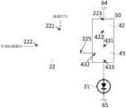
图8为本发明实施例提供的一种脉宽调制芯片的结构示意图,如图8所示, 可选的,脉宽调制芯片22包括数据信号端221、扫描信号端222、恒流电源输 入端223以及输出端224,脉宽调制芯片22的输出端224与LED单元21电连 接,脉宽调制芯片22用于在扫描信号端222输入有效扫描脉冲时启动,并根据数据信号端221输入的数据信号,调节与之电连接的LED单元21的发光时长。Figure 8 is a schematic structural diagram of a pulse width modulation chip provided by an embodiment of the present invention, as shown in Figure 8, optionally, the pulsewidth modulation chip 22 includes adata signal terminal 221, ascanning signal terminal 222, a constant currentpower input terminal 223 andoutput terminal 224, theoutput terminal 224 of the pulsewidth modulation chip 22 is electrically connected with theLED unit 21, and the pulsewidth modulation chip 22 is used to start when thescanning signal terminal 222 inputs an effective scanning pulse, and according to the data signal terminal 221 input data signal to adjust the light-emitting duration of theLED unit 21 electrically connected thereto.

具体的,脉宽调制芯片22的数据信号端221用于接收数据信号,扫描信号 端222用于接收有效扫描脉冲,恒流电源输入端223用于输入正性电源,输出 端224用于向LED单元21输出恒定驱动电流,脉宽调制芯片22在扫描信号端 222输入有效扫描脉冲时启动,并根据数据信号端221输入的数据信号,调节 与之电连接的LED单元21的发光时长,从而实现控制LED单元21的显示灰阶。Specifically, the data signalterminal 221 of the pulsewidth modulation chip 22 is used for receiving data signals, thescanning signal terminal 222 is used for receiving effective scanning pulses, the constant current powersupply input terminal 223 is used for inputting a positive power supply, and theoutput terminal 224 is used for supplying positive power to the LED. Theunit 21 outputs a constant drive current, and the pulsewidth modulation chip 22 starts when thescan signal terminal 222 inputs an effective scan pulse, and adjusts the light-emitting duration of theLED unit 21 electrically connected to it according to the data signal input from the data signal terminal 221, thereby realizing The display grayscale of theLED unit 21 is controlled.

图9为本发明实施例提供的另一种脉宽调制芯片的结构示意图,如图9所 示,脉宽调制芯片22包括脉宽调制单元41、恒流单元42和开关单元43,脉宽 调制单元41包括数据信号端221和扫描信号端222,恒流单元42包括恒流电 源输入端223,恒流单元42的输出端422与开关单元43的第一端431电连接, 恒流单元42用于向开关单元43输入恒定驱动电流。开关单元43的控制端432 与脉宽调制单元41的输出端413电连接,开关单元43的第二端433为脉宽调 制芯片22的输出端224,脉宽调制单元41用于在扫描信号端222输入有效扫描脉冲时启动,并根据数据信号端221输入的数据信号,调节输出脉冲信号的 脉宽,开关单元43用于根据脉冲信号控制LED单元21的发光时长。Fig. 9 is a schematic structural diagram of another pulse width modulation chip provided by an embodiment of the present invention. As shown in Fig. 9, the pulsewidth modulation chip 22 includes a pulsewidth modulation unit 41, a constantcurrent unit 42 and aswitch unit 43, and the pulsewidth modulation Unit 41 includes data signalend 221 and scansignal end 222, constantcurrent unit 42 includes constant current powersupply input end 223, theoutput end 422 of constantcurrent unit 42 is electrically connected with thefirst end 431 ofswitch unit 43, constantcurrent unit 42 Used to input a constant driving current to theswitch unit 43 . Thecontrol terminal 432 of theswitch unit 43 is electrically connected with theoutput terminal 413 of the pulsewidth modulation unit 41, thesecond terminal 433 of theswitch unit 43 is theoutput terminal 224 of the pulsewidth modulation chip 22, and the pulsewidth modulation unit 41 is used for scanningsignal Terminal 222 starts when valid scan pulse is input, and adjusts the pulse width of the output pulse signal according to the data signal input by data signal terminal 221, and switchunit 43 is used to control the light-emitting duration ofLED unit 21 according to the pulse signal.

具体的,恒流单元42和开关单元43位于脉宽调制芯片22内,脉宽调制单 元41的数据信号端221作为脉宽调制芯片22的数据信号端221,用于接收数 据信号,脉宽调制单元41的扫描信号端222作为脉宽调制芯片22的扫描信号 端222,用于接收有效扫描脉冲,恒流单元42的恒流电源输入端223作为脉宽 调制芯片22的恒流电源输入端223,用于输入正性电源,开关单元43的第二 端433作为脉宽调制芯片22的输出端224,用于向LED单元21输出恒定驱动 电流。Specifically, the constantcurrent unit 42 and theswitch unit 43 are located in the pulsewidth modulation chip 22, and the data signalend 221 of the pulsewidth modulation unit 41 is used as the data signalend 221 of the pulsewidth modulation chip 22 for receiving data signals, pulse Thescan signal end 222 of thewidth modulation unit 41 is used as thescan signal end 222 of the pulsewidth modulation chip 22 for receiving effective scan pulses, and the constant currentpower input end 223 of the constantcurrent unit 42 is used as the constant current power input of the pulsewidth modulation chip 22 The terminal 223 is used to input positive power, and thesecond terminal 433 of theswitch unit 43 is used as theoutput terminal 224 of the pulsewidth modulation chip 22 to output a constant driving current to theLED unit 21.

脉宽调制单元41在扫描信号端222输入有效扫描脉冲时启动,并根据数据 信号端221输入的数据信号,调节输出脉冲信号的脉宽。恒流单元42用于向开 关单元43输入恒定驱动电流,开关单元43根据接收的脉冲信号处于导通状态 或断开状态,当开关单元43处于导通状态时,恒流单元42提供的恒定驱动电 流经过开关单元43传输至LED单元21,从而驱动LED单元21发光;当开关单 元43处于断开状态时,恒流单元42提供的恒定驱动电流无法经过开关单元43 传输至LED单元21,LED单元21不发光。因此,通过调节输出脉冲信号的脉宽, 能够控制开关单元43的导通时长,进而能够控制LED单元21的发光时长,实 现控制LED单元21的显示灰阶。The pulsewidth modulation unit 41 starts when thescan signal terminal 222 inputs an effective scan pulse, and adjusts the pulse width of the output pulse signal according to the data signal input by the data signalterminal 221. The constantcurrent unit 42 is used to input a constant driving current to theswitch unit 43, and theswitch unit 43 is in a conduction state or a disconnection state according to the received pulse signal. When theswitch unit 43 is in a conduction state, the constantcurrent unit 42 provides a constant The drive current is transmitted to theLED unit 21 through theswitch unit 43, thereby driving theLED unit 21 to emit light; when theswitch unit 43 is in an off state, the constant drive current provided by the constantcurrent unit 42 cannot be transmitted to theLED unit 21 through theswitch unit 43 , theLED unit 21 does not emit light. Therefore, by adjusting the pulse width of the output pulse signal, the conduction time of theswitch unit 43 can be controlled, and then the light-emitting time of theLED unit 21 can be controlled, so as to control the display gray scale of theLED unit 21.

本发明实施例提供的显示面板,将数据信号转化为开关单元43的导通时长, 通过控制LED单元21的发光时长来控制显示灰阶,对于不同的显示灰阶,流过 LED单元21的恒定驱动电流大小相同,实现LED单元21的恒流驱动,进而可 以充分利用LED单元21大电流时高发光效率的特性,可以使得在包括低灰阶范 围的任意灰阶内,LED单元21的发光效率都较高,进而避免低灰阶范围内因LED 单元21发光效率低而达不到预期发光亮度而影响显示效果。The display panel provided by the embodiment of the present invention converts the data signal into the conduction time of theswitch unit 43, and controls the display gray scale by controlling the light emitting time of theLED unit 21. For different display gray scales, the constant light flowing through theLED unit 21 The drive currents have the same magnitude to realize the constant current drive of theLED unit 21, and then can make full use of the characteristics of high luminous efficiency of theLED unit 21 when the current is large, so that theLED unit 21 can be used in any gray scale including the low gray scale range. The luminous efficiency is high, thereby avoiding the display effect being affected by the low luminous efficiency of theLED unit 21 and the expected luminous brightness not being achieved in the low gray scale range.

可选的,图10为本发明实施例提供的一种显示面板的局部剖面结构示意图, 图11为本发明实施例提供的又一种脉宽调制芯片的结构示意图,如图10和图 11所示,衬底20包括衬底基板201和位于衬底基板201一侧的多个恒流开关 单元50,多个恒流开关单元50与多个脉宽调制芯片22一一对应,恒流开关单 元50包括恒流单元42和开关单元43,脉宽调制芯片22通过恒流开关单元50 与LED单元21电连接,脉宽调制芯片22包括数据信号端221、扫描信号端222 以及输出端225,脉宽调制芯片22的输出端225与开关单元43的控制端432 电连接,开关单元43的第一端431与恒流单元42的输出端422电连接,恒流 单元43包括恒流电源输入端223,恒流单元42用于向开关单元43输入恒定驱 动电流。开关单元43的第二端433与LED单元21电连接,脉宽调制芯片22用于在扫描信号端222输入有效扫描脉冲时启动,并根据数据信号端221输入的 数据信号,调节向与之电连接的开关单元43输出的脉冲信号的脉宽,以使开关 单元43根据脉冲信号控制LED单元21的发光时长。Optionally, FIG. 10 is a schematic partial cross-sectional structure diagram of a display panel provided by an embodiment of the present invention, and FIG. 11 is a schematic structural diagram of another pulse width modulation chip provided by an embodiment of the present invention, as shown in FIG. 10 and FIG. 11 As shown, thesubstrate 20 includes asubstrate substrate 201 and a plurality of constantcurrent switch units 50 located on one side of thesubstrate substrate 201, the plurality of constantcurrent switch units 50 correspond to a plurality of pulsewidth modulation chips 22 one by one, and the constant currentswitch units Unit 50 includes constantcurrent unit 42 andswitch unit 43, pulsewidth modulation chip 22 is electrically connected withLED unit 21 through constantcurrent switch unit 50, pulsewidth modulation chip 22 includes data signalend 221, scanningsignal end 222 andoutput end 225, Theoutput terminal 225 of the pulsewidth modulation chip 22 is electrically connected to thecontrol terminal 432 of theswitch unit 43, thefirst terminal 431 of theswitch unit 43 is electrically connected to theoutput terminal 422 of the constantcurrent unit 42, and the constantcurrent unit 43 includes a constant current powersupply input terminal 223. The constantcurrent unit 42 is used to input a constant driving current to theswitch unit 43. Thesecond terminal 433 of theswitch unit 43 is electrically connected to theLED unit 21, and the pulsewidth modulation chip 22 is used to start when thescanning signal terminal 222 inputs an effective scanning pulse, and adjusts the current flow to theLED unit 221 according to the data signal input from the data signalterminal 221. The pulse width of the pulse signal output by theconnected switch unit 43, so that theswitch unit 43 controls the light-emitting duration of theLED unit 21 according to the pulse signal.

具体的,恒流单元42的恒流电源输入端223用于输入正性电源,脉宽调制 芯片22的数据信号端221用于接收数据信号,脉宽调制芯片22的扫描信号端 222用于接收有效扫描脉冲。恒流单元42的输出端422与开关单元43的第一 端431电连接,恒流单元42用于向开关单元43输入恒定驱动电流。脉宽调制 芯片22在扫描信号端222输入有效扫描脉冲时启动,并根据数据信号端221输 入的数据信号,调节向与之电连接的开关单元43输出的脉冲信号的脉宽,开关 单元43根据接收的脉冲信号处于导通状态或断开状态,当开关单元43处于导通状态时,恒流单元42提供的恒定驱动电流经过开关单元43传输至LED单元 21,从而驱动LED单元21发光;当开关单元43处于断开状态时,恒流单元42 提供的恒定驱动电流无法经过开关单元43传输至LED单元21,LED单元21不 发光。因此,通过脉宽调制芯片22调节输出脉冲信号的脉宽,能够控制开关单 元43的导通时长,进而能够控制LED单元21的发光时长,实现控制LED单元 21的显示灰阶。Specifically, the constant current powersupply input terminal 223 of the constantcurrent unit 42 is used for inputting positive power, the data signalterminal 221 of the pulsewidth modulation chip 22 is used for receiving data signals, and thescan signal terminal 222 of the pulsewidth modulation chip 22 is used for receiving Active scan pulse. Theoutput end 422 of the constantcurrent unit 42 is electrically connected to thefirst end 431 of theswitch unit 43, and the constantcurrent unit 42 is used to input a constant driving current to theswitch unit 43. The pulsewidth modulation chip 22 starts when thescan signal terminal 222 inputs an effective scan pulse, and adjusts the pulse width of the pulse signal output to theswitch unit 43 electrically connected to it according to the data signal input by the data signal terminal 221, theswitch unit 43 According to whether the received pulse signal is on or off, when theswitch unit 43 is in the on state, the constant drive current provided by the constantcurrent unit 42 is transmitted to theLED unit 21 through theswitch unit 43, thereby driving theLED unit 21 to emit light; When theswitch unit 43 is in the disconnected state, the constant drive current provided by the constantcurrent unit 42 cannot be transmitted to theLED unit 21 through theswitch unit 43, and theLED unit 21 does not emit light. Therefore, by adjusting the pulse width of the output pulse signal through the pulsewidth modulation chip 22, the conduction time of theswitch unit 43 can be controlled, and then the light-emitting time of theLED unit 21 can be controlled, so as to control the display gray scale of theLED unit 21.

需要注意的是,恒流开关单元50可以与脉宽调制芯片22设置于衬底基板 201的同一侧,也可以与脉宽调制芯片22设置于衬底基板201的不同侧,图10 以恒流开关单元50与脉宽调制芯片22设置于衬底基板201的不同侧为例,本 发明实施例对此不作限定。It should be noted that the constantcurrent switch unit 50 can be arranged on the same side of thebase substrate 201 as the pulsewidth modulation chip 22, or can be arranged on a different side of thebase substrate 201 with the pulsewidth modulation chip 22. FIG. 10 uses constant current Theswitch unit 50 and the pulsewidth modulation chip 22 are disposed on different sides of thebase substrate 201 as an example, which is not limited in this embodiment of the present invention.

图12为本发明实施例提供的又一种脉宽调制芯片的结构示意图,如图12 所示,可选的,开关单元43包括开关晶体管44,开关晶体管44的第一极441 与恒流单元42的输出端422电连接,开关晶体管44的第二极442与LED单元 21电连接。Figure 12 is a structural schematic diagram of another pulse width modulation chip provided by the embodiment of the present invention, as shown in Figure 12, optionally, theswitch unit 43 includes aswitch transistor 44, the first pole 441 of theswitch transistor 44 and the constant current unit Theoutput terminal 422 of 42 is electrically connected, and the second pole 442 of the switchingtransistor 44 is electrically connected with theLED unit 21.

具体的,开关单元43可采用开关晶体管44,开关晶体管44的第一极441 作为开关单元43的第一端431,开关晶体管44的第二极442作为开关单元43 的第二端433,开关晶体管44还包括控制端443,开关晶体管44的控制端443 作为开关单元43的控制端432。恒流单元42用于向开关晶体管44的第一极441 输入恒定驱动电流,脉宽调制芯片22在扫描信号端222输入有效扫描脉冲时启 动,并根据数据信号端221输入的数据信号,调节脉冲信号的脉宽,并将脉冲 信号输入开关晶体管44的控制端443,开关晶体管44根据控制端443接收的脉冲信号处于导通状态或断开状态,当开关单元43处于导通状态时,恒流单元 42提供的恒定驱动电流经过开关单元43传输至LED单元21,从而驱动LED单 元21发光;当开关单元43处于断开状态时,恒流单元42提供的恒定驱动电流 无法经过开关单元43传输至LED单元21,LED单元21不发光。因此,通过脉 宽调制芯片22调节输出脉冲信号的脉宽,能够控制开关晶体管44的导通时长, 进而能够控制LED单元21的发光时长,实现控制LED单元21的显示灰阶。Specifically, theswitch unit 43 can adopt aswitch transistor 44, the first pole 441 of theswitch transistor 44 is used as thefirst end 431 of theswitch unit 43, the second pole 442 of theswitch transistor 44 is used as thesecond end 433 of theswitch unit 43, and theswitch transistor 44 also includes a control terminal 443, the control terminal 443 of the switchingtransistor 44 is used as thecontrol terminal 432 of theswitch unit 43. The constantcurrent unit 42 is used to input a constant drive current to the first pole 441 of the switchingtransistor 44, and the pulsewidth modulation chip 22 starts when thescan signal terminal 222 inputs an effective scan pulse, and adjusts according to the data signal input by the data signalterminal 221. pulse width of the pulse signal, and the pulse signal is input to the control terminal 443 of the switchingtransistor 44, the switchingtransistor 44 is in the conducting state or the disconnecting state according to the pulse signal received by the control terminal 443, when the switchingunit 43 is in the conducting state, the constant The constant drive current provided by thecurrent unit 42 is transmitted to theLED unit 21 through theswitch unit 43, thereby driving theLED unit 21 to emit light; when theswitch unit 43 is in an off state, the constant drive current provided by the constantcurrent unit 42 cannot pass through theswitch unit 43 transmitted to theLED unit 21, theLED unit 21 does not emit light. Therefore, by adjusting the pulse width of the output pulse signal through the pulsewidth modulation chip 22, the conduction duration of the switchingtransistor 44 can be controlled, and then the light-emitting duration of theLED unit 21 can be controlled, so as to realize controlling the display gray scale of theLED unit 21.

其中,开关晶体管44包括薄膜晶体管,薄膜晶体管可以为n型薄膜晶体管 或p型薄膜晶体管,薄膜晶体管的类型可以包括非晶硅薄膜晶体管、氧化物薄 膜晶体管和多晶硅薄膜晶体管,本领域技术人员可根据实际需求进行设置。Wherein, theswitch transistor 44 includes a thin film transistor, and the thin film transistor can be an n-type thin film transistor or a p-type thin film transistor, and the type of the thin film transistor can include an amorphous silicon thin film transistor, an oxide thin film transistor, and a polysilicon thin film transistor. Set according to actual needs.

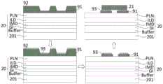
具体的,图13为本发明实施例提供的另一种显示面板的局部剖面结构示意 图,如图13所示,以恒流开关单元50与脉宽调制芯片22设置于衬底基板201 的不同侧为例,恒流开关单元50中的开关晶体管44设置于衬底基板201背离脉宽调制芯片22(图中未示出)的一侧。开关晶体管44包括薄膜晶体管51, 薄膜晶体管51包括层叠设置于衬底基板201一侧的缓冲层Buffer、栅极绝缘 层GI、金属绝缘层IMD、层间绝缘层ILD、平坦化层PLN、以及位于缓冲层Buffer 远离衬底基板201一侧的有源层52、位于栅极绝缘层GI远离衬底基板201一 侧的栅极金属层53、位于层间绝缘层ILD远离衬底基板201一侧的源漏极金属 层54;源漏极金属层54通过设置在栅极绝缘层GI、金属绝缘层IMD和层间绝缘层ILD上的过孔与有源层52电连接,LED单元21通过设置在平坦化层PLN 上的过孔与源漏极金属层54电连接。其中,LED单元21与源漏极金属层54之 间还可包括共晶电极层60,以使LED单元21通过共晶键合方式与源漏极金属 层54电连接。Specifically, FIG. 13 is a schematic diagram of a partial cross-sectional structure of another display panel provided by an embodiment of the present invention. As shown in FIG. Taking the side as an example, the switchingtransistor 44 in the constantcurrent switching unit 50 is disposed on the side of thebase substrate 201 away from the pulse width modulation chip 22 (not shown in the figure). The switchingtransistor 44 includes athin film transistor 51, and thethin film transistor 51 includes a buffer layer Buffer stacked on one side of thebase substrate 201, a gate insulating layer GI, a metal insulating layer IMD, an interlayer insulating layer ILD, a planarization layer PLN, and a The buffer layer Buffer is theactive layer 52 on the side away from thebase substrate 201, thegate metal layer 53 on the side of the gate insulating layer GI away from thebase substrate 201, and thegate metal layer 53 on the side of the interlayer insulating layer ILD away from thebase substrate 201. The source-drain metal layer 54; the source-drain metal layer 54 is electrically connected to theactive layer 52 through the via holes arranged on the gate insulating layer GI, the metal insulating layer IMD and the interlayer insulating layer ILD, and theLED unit 21 is arranged on the The vias on the planarization layer PLN are electrically connected to the source-drain metal layer 54. Wherein, aeutectic electrode layer 60 may also be included between theLED unit 21 and the source-drain metal layer 54, so that theLED unit 21 is electrically connected to the source-drain metal layer 54 by eutectic bonding.

图14为本发明实施例提供的又一种显示面板的局部剖面结构示意图,如图 14所示,以恒流开关单元50与脉宽调制芯片22设置于衬底20的同一侧为例, 恒流开关单元50中的开关晶体管44设置于衬底20靠近脉宽调制芯片22(图 中未示出)的一侧。开关晶体管44包括薄膜晶体管51,薄膜晶体管51包括设 置于衬底20一侧的缓冲层Buffer、栅极绝缘层GI、金属绝缘层IMD、层间绝 缘层ILD、平坦化层PLN、以及位于缓冲层Buffer靠近衬底20一侧的有源层52、位于栅极绝缘层GI靠近衬底20一侧的栅极金属层53、位于层间绝缘层ILD靠近衬底20一侧的源漏极金属层54;源漏极金属层54通过设置在栅极绝缘层 GI、金属绝缘层IMD和层间绝缘层ILD上的过孔与有源层52电连接,LED单元 21通过设置在平坦化层PLN和衬底20上的过孔与源漏极金属层54电连接。其 中,LED单元21与源漏极金属层54之间还可包括共晶电极层60,以使LED单元21通过共晶键合方式与源漏极金属层54电连接。FIG. 14 is a partial cross-sectional structural schematic diagram of another display panel provided by an embodiment of the present invention. As shown in FIG. Theswitch transistor 44 in theflow switch unit 50 is arranged on the side of thesubstrate 20 close to the pulse width modulation chip 22 (not shown in the figure). Theswitch transistor 44 includes athin film transistor 51, and thethin film transistor 51 includes a buffer layer Buffer disposed on one side of thesubstrate 20, a gate insulating layer GI, a metal insulating layer IMD, an interlayer insulating layer ILD, a planarization layer PLN, and a Theactive layer 52 of the buffer layer Buffer close to thesubstrate 20, thegate metal layer 53 located on the side of the gate insulating layer GI close to thesubstrate 20, the source and drain electrodes located on the side of the interlayer insulating layer ILD close to thesubstrate 20Metal layer 54; the source-drain metal layer 54 is electrically connected to theactive layer 52 through the via holes arranged on the gate insulating layer GI, the metal insulating layer IMD and the interlayer insulating layer ILD, and theLED unit 21 is arranged on the planarization layer The vias on the PLN and thesubstrate 20 are electrically connected to the source-drain metal layer 54 . Wherein, aeutectic electrode layer 60 may also be included between theLED unit 21 and the source-drain metal layer 54, so that theLED unit 21 is electrically connected to the source-drain metal layer 54 through eutectic bonding.

继续参考图13和图14,可选的,显示面板还包括位于LED单元21远离衬 底20一侧的封装层TFE,封装层TFE可起到隔绝外界水汽,保护LED单元21 的作用。Continuing to refer to FIGS. 13 and 14 , optionally, the display panel further includes an encapsulation layer TFE located on the side of theLED unit 21 away from thesubstrate 20. The encapsulation layer TFE can play a role of isolating external moisture and protecting theLED unit 21.

图15为本发明实施例提供的又一种脉宽调制芯片的结构示意图,如图15 所示,可选的,脉宽调制芯片22包括寄存器226和状态机227,寄存器226与 数据信号端221电连接,状态机227分别与扫描信号端222、寄存器226以及 开关单元43电连接。状态机227用于根据扫描信号端222输入的扫描信号控制 状态机227启动或关闭,寄存器226用于存储数据信号端221输入的数据信号, 状态机227还用于根据扫描信号端222输入的扫描信号以及从寄存器226中读 取的数据信号调节输出脉冲信号的脉宽。Fig. 15 is the structural representation of another kind of pulse width modulation chip that the embodiment of the present invention provides, as shown in Fig. 15, optional, pulsewidth modulation chip 22 comprises register 226 andstate machine 227, register 226 and data signalend 221 Electrically connected, thestate machine 227 is electrically connected to thescan signal terminal 222, the register 226 and theswitch unit 43 respectively. Thestate machine 227 is used to control the start or close of thestate machine 227 according to the scan signal input by thescan signal terminal 222, the register 226 is used to store the data signal input by the data signal terminal 221, and thestate machine 227 is also used to scan according to thescan signal terminal 222 input signal and the data signal read from register 226 adjust the pulse width of the output pulse signal.

其中,数据信号先传输至寄存器226,寄存器226用于存储数据信号,状 态机227用于根据扫描信号端222输入的扫描信号控制状态机227启动或关闭, 状态机227还用于根据扫描信号端222输入的扫描信号以及从寄存器226中读 取的数据信号调节输出脉冲信号的脉宽。具体的,扫描信号包括有效扫描脉冲, 状态机227在扫描信号端222输入有效扫描脉冲时启动,并根据从寄存器226 中读取的数据信号,调节向与之电连接的开关单元43输出的脉冲信号的脉宽, 开关单元43根据接收的脉冲信号处于导通状态或断开状态,当开关单元43处于导通状态时,恒流单元42提供的恒定驱动电流经过开关单元43传输至LED 单元21,从而驱动LED单元21发光;当开关单元43处于断开状态时,恒流单 元42提供的恒定驱动电流无法经过开关单元43传输至LED单元21,LED单元 21不发光。因此,通过状态机227调节输出脉冲信号的脉宽,能够控制开关单元43的导通时长,进而能够控制LED单元21的发光时长,实现控制LED单元 21的显示灰阶。Wherein, the data signal is first transmitted to the register 226, the register 226 is used to store the data signal, thestate machine 227 is used to control thestate machine 227 to start or close according to the scan signal input by thescan signal terminal 222, and thestate machine 227 is also used to control thestate machine 227 according to the scan signal The scan signal input from the terminal 222 and the data signal read from the register 226 adjust the pulse width of the output pulse signal. Specifically, the scan signal includes an effective scan pulse, and thestate machine 227 starts when thescan signal terminal 222 inputs an effective scan pulse, and adjusts the pulse output to theswitch unit 43 electrically connected to it according to the data signal read from the register 226 The pulse width of the signal, theswitch unit 43 is in the on state or the off state according to the received pulse signal, when theswitch unit 43 is in the on state, the constant driving current provided by the constantcurrent unit 42 is transmitted to theLED unit 21 through theswitch unit 43 , thereby driving theLED unit 21 to emit light; when theswitch unit 43 is in an off state, the constant drive current provided by the constantcurrent unit 42 cannot be transmitted to theLED unit 21 through theswitch unit 43, and theLED unit 21 does not emit light. Therefore, by adjusting the pulse width of the output pulse signal through thestate machine 227, the conduction time of theswitch unit 43 can be controlled, and then the light-emitting time of theLED unit 21 can be controlled, so as to realize the display gray scale control of theLED unit 21.

图16为本发明实施例提供的一种脉宽调制芯片的工作流程示意图,如图 16所示,可选的,状态机227包括PWM信号开关单元61、信号同步单元62和 PWM信号产生单元63,PWM信号开关单元61根据接收到的扫描信号而启动,并 产生使能信号。信号同步单元62获取驱动芯片23的行同步信号,并在接收到行同步信号的下降沿时将PWM信号开关单元61产生的使能信号输出至PWM信号 产生单元63。PWM信号产生单元63接收到使能信号后,根据数据信号产生对应 脉宽的脉宽调制(Pulse Width Modulation,PWM)信号,进而控制LED单元21的发光时长,实现控制LED单元21的显示灰阶。Figure 16 is a schematic diagram of the workflow of a pulse width modulation chip provided by an embodiment of the present invention, as shown in Figure 16, optionally, thestate machine 227 includes a PWMsignal switching unit 61, asignal synchronization unit 62 and a PWMsignal generating unit 63 , the PWMsignal switching unit 61 starts according to the received scan signal, and generates an enabling signal. Thesignal synchronizing unit 62 obtains the horizontal synchronizing signal of thedriving chip 23, and outputs the enabling signal generated by the PWMsignal switching unit 61 to the PWMsignal generating unit 63 when receiving the falling edge of the horizontal synchronizing signal. After the PWMsignal generation unit 63 receives the enable signal, it generates a pulse width modulation (Pulse Width Modulation, PWM) signal corresponding to the pulse width according to the data signal, and then controls the light-emitting duration of theLED unit 21, so as to realize the control of the display gray scale of theLED unit 21. .

图17为本发明实施例提供的又一种显示面板的结构示意图,如图8和图 17所示,可选的,衬底20上还设置有多条正性电源信号线64,正性电源信号 线64与恒流电源输入端233电连接,正性电源信号线64与脉宽调制芯片22位 于衬底20的同一侧。Fig. 17 is a schematic structural diagram of another display panel provided by an embodiment of the present invention, as shown in Fig. 8 and Fig. 17, optionally, a plurality of positive powersupply signal lines 64 are also arranged on thesubstrate 20, and the positive power supply Thesignal line 64 is electrically connected to the constant current power supply input terminal 233, and the positive powersupply signal line 64 and the pulsewidth modulation chip 22 are located on the same side of thesubstrate 20.

具体的,正性电源信号线64与恒流电源输入端233电连接,从而为恒流单 元42提供正性电源,恒流单元42用于将正性电源转换为恒定驱动电流,其中, 正性电源可以为PVDD电源电压。将正性电源信号线64与脉宽调制芯片22设置 于衬底20的同一侧,以使正性电源信号线64可与脉宽调制芯片22直接连接, 无需在衬底20上额外制作过孔,有助于减少制备工艺步骤,降低制备成本。Specifically, the positive powersupply signal line 64 is electrically connected to the constant current power supply input terminal 233, thereby providing a positive power supply for the constantcurrent unit 42, and the constantcurrent unit 42 is used to convert the positive power supply into a constant drive current, wherein the positive The neutral power supply may be a PVDD supply voltage. The positivepower signal line 64 and the pulsewidth modulation chip 22 are arranged on the same side of thesubstrate 20, so that the positivepower signal line 64 can be directly connected to the pulsewidth modulation chip 22, without making additional via holes on thesubstrate 20 , helping to reduce the preparation process steps and reduce the preparation cost.

图18为本发明实施例提供的另一种显示面板的第一侧的结构示意图,图 19为本发明实施例提供的另一种显示面板的第二侧的结构示意图,如图8、图 18和图19所示,可选的,衬底20上还设置有多条正性电源信号线64,衬底 20还包括多个第四过孔34,正性电源信号线64与脉宽调制芯片22位于衬底 20的不同侧,正性电源信号线64通过第四过孔34与恒流电源输入端223电连 接。Fig. 18 is a schematic structural view of the first side of another display panel provided by an embodiment of the present invention, and Fig. 19 is a schematic structural view of a second side of another display panel provided by an embodiment of the present invention, as shown in Fig. 8 and Fig. 18 As shown in Figure 19, optionally, thesubstrate 20 is also provided with a plurality of positive power signal lines 64, thesubstrate 20 also includes a plurality of fourth via holes 34, the positive power signal lines 64 and the pulsewidth modulation chip 22 are located on different sides of thesubstrate 20, and the positivepower signal line 64 is electrically connected to the constant currentpower input terminal 223 through the fourth via hole 34.

具体的,正性电源信号线64位于衬底20的第一侧203,脉宽调制芯片22 位于衬底20的第二侧204,正性电源信号线64通过第四过孔34与恒流电源输 入端223电连接,从而为恒流单元42提供正性电源。Specifically, the positivepower signal line 64 is located on thefirst side 203 of thesubstrate 20, the pulsewidth modulation chip 22 is located on thesecond side 204 of thesubstrate 20, and the positivepower signal line 64 is connected to the constant current power supply through the fourth via hole 34. Theinput terminal 223 is electrically connected to provide a positive power supply for the constantcurrent unit 42.

图20为本发明实施例提供的又一种显示面板的局部剖面结构示意图,如图 11和图20所示,衬底20上还设置有多条正性电源信号线64,正性电源信号线 64与恒流开关单元50位于衬底基板201的同一侧。Fig. 20 is a partial cross-sectional structural schematic diagram of another display panel provided by an embodiment of the present invention. As shown in Fig. 11 and Fig. 20, a plurality of positive power signal lines 64 are arranged on thesubstrate 20, and the positive power signal lines 64 is located on the same side of thebase substrate 201 as the constantcurrent switch unit 50 .

具体的,正性电源信号线64与恒流开关单元50的恒流电源输入端223电 连接,从而为恒流开关单元50提供正性电源。将正性电源信号线64与恒流开 关单元50设置于衬底基板201的同一侧,以使正性电源信号线64可与恒流开 关单元50直接连接,无需在衬底基板201上额外制作过孔,有助于减少制备工 艺步骤,降低制备成本。Specifically, the positive powersupply signal line 64 is electrically connected to the constant currentpower input terminal 223 of the constantcurrent switch unit 50, thereby providing a positive power supply for the constantcurrent switch unit 50. The positivepower signal line 64 and the constantcurrent switch unit 50 are arranged on the same side of thebase substrate 201, so that the positivepower signal line 64 can be directly connected to the constantcurrent switch unit 50, without the need for the constantcurrent switch unit 50 on thebase substrate 201 Making additional via holes helps to reduce the number of manufacturing process steps and lower the manufacturing cost.

图21为本发明实施例提供的又一种显示面板的局部剖面结构示意图,如图 11和图21所示,可选的,衬底20上还设置有多条正性电源信号线64,衬底 20还包括多个第五过孔35,正性电源信号线64与恒流开关单元50位于衬底基 板201的不同侧,正性电源信号线64通过第五过孔35与恒流电源输入端223 电连接。Fig. 21 is a partial cross-sectional structural schematic diagram of another display panel provided by an embodiment of the present invention, as shown in Fig. 11 and Fig. 21, optionally, a plurality of positive powersupply signal lines 64 are arranged on thesubstrate 20, and the substrate The bottom 20 also includes a plurality of fifth via holes 35, the positivepower signal line 64 and the constantcurrent switch unit 50 are located on different sides of thebase substrate 201, and the positivepower signal line 64 is connected to the constant current power supply through the fifth via hole 35. Theinput terminal 223 is electrically connected.

具体的,恒流开关单元50和正性电源信号线64分别位于衬底基板201的 不同侧,正性电源信号线64通过第五过孔35与恒流开关单元50电连接,从而 为恒流开关单元50提供正性电源。Specifically, the constantcurrent switch unit 50 and the positivepower signal line 64 are respectively located on different sides of thebase substrate 201, and the positivepower signal line 64 is electrically connected to the constantcurrent switch unit 50 through the fifth via hole 35, thereby forming a constant current switch.Unit 50 provides a positive power supply.

图22为本发明实施例提供的又一种显示面板的结构示意图,如图9和图 22所示,可选的,衬底20上还设置有多条负性电源信号线65,各LED单元21 与负性电源信号线65电连接。Fig. 22 is a schematic structural diagram of another display panel provided by an embodiment of the present invention, as shown in Fig. 9 and Fig. 22, optionally, a plurality of negative powersupply signal lines 65 are also arranged on thesubstrate 20, and eachLED unit 21 is electrically connected with the negative powersupply signal line 65.

具体的,负性电源信号线65与LED单元21电连接,为LED单元21提供负 性电源,从而在LED单元21发光时提供电流回路,其中,负性电源可以为PVEE 电源电压或者GND。Specifically, the negative powersupply signal line 65 is electrically connected to theLED unit 21 to provide a negative power supply for theLED unit 21, thereby providing a current loop when theLED unit 21 emits light, wherein the negative power supply can be PVEE power supply voltage or GND.

继续参考图22,可选的,负性电源信号线65与LED单元21位于衬底20 的同一侧。Continuing to refer to FIG. 22, optionally, the negativepower signal line 65 and theLED unit 21 are located on the same side of thesubstrate 20.

其中,通过将负性电源信号线65与LED单元21设置于衬底20的同一侧, 以使负性电源信号线65可与LED单元21直接连接,无需在衬底20上额外制作 过孔,有助于减少制备工艺步骤,降低制备成本。Wherein, by arranging the negativepower signal line 65 and theLED unit 21 on the same side of thesubstrate 20, the negativepower signal line 65 can be directly connected to theLED unit 21, without making additional via holes on thesubstrate 20, It is helpful to reduce the preparation process steps and reduce the preparation cost.

图23为本发明实施例提供的又一种显示面板的第一侧的结构示意图,图 24为本发明实施例提供的又一种显示面板的第二侧的结构示意图,如图23和 图24所示,可选的,负性电源信号线65与LED单元21位于衬底20的不同侧, 衬底20包括多个第六过孔36,负性电源信号线65通过第六过孔36与LED单 元21电连接。Fig. 23 is a schematic structural view of the first side of another display panel provided by an embodiment of the present invention, and Fig. 24 is a schematic structural view of a second side of another display panel provided by an embodiment of the present invention, as shown in Fig. 23 and Fig. 24 As shown, optionally, the negativepower signal line 65 and theLED unit 21 are located on different sides of thesubstrate 20, thesubstrate 20 includes a plurality of sixth viaholes 36, and the negativepower signal line 65 passes through the sixth viahole 36 and TheLED unit 21 is electrically connected.

具体的,LED单元21位于衬底20的第一侧203,负性电源信号线65位于 衬底20的第二侧204,负性电源信号线65通过第六过孔36与LED单元21电 连接,从而在LED单元21发光时提供电流回路。Specifically, theLED unit 21 is located on thefirst side 203 of thesubstrate 20, the negativepower signal line 65 is located on thesecond side 204 of thesubstrate 20, and the negativepower signal line 65 is electrically connected to theLED unit 21 through the sixth viahole 36 , so as to provide a current loop when theLED unit 21 emits light.

图25为本发明实施例提供的又一种显示面板的局部结构示意图,如图25 所示,可选的,本发明实施例提供的显示面板包括阵列排布的多个子像素70, 每个子像素70包括一LED单元21和一脉宽调制芯片22,每个LED单元21包 括N个LED子单元211,同一子像素70中的N个LED子单元211分别与该子像 素70的脉宽调制芯片22电连接,N为大于1的正整数。Figure 25 is a partial structural schematic diagram of another display panel provided by an embodiment of the present invention, as shown in Figure 25, optionally, the display panel provided by this embodiment of the present invention includes a plurality of sub-pixels 70 arranged in an array, each sub-pixel 70 includes anLED unit 21 and a pulsewidth modulation chip 22, eachLED unit 21 includesN LED subunits 211, and theN LED subunits 211 in thesame subpixel 70 are respectively equal to the pulse width of thesubpixel 70 Themodulation chip 22 is electrically connected, and N is a positive integer greater than 1.

具体的,每个子像素70包括N个LED子单元211,N个LED子单元211分 别与一个脉宽调制芯片22电连接,以使脉宽调制芯片22分别控制N个LED子 单元211的显示灰阶,N个LED子单元211的显示灰阶可以不同,从而可以实 现更高灰阶分辨率。示例性的,如图25所示,以子像素70包括2个LED子单 元211为例,脉宽调制芯片22可控制2个LED子单元211分别以不同的显示灰 阶进行显示,2个LED子单元211组合则可提高一倍的灰阶数,假设每个LED单元21能够实现的灰阶数为8bit,2个LED子单元211组合的灰阶数达到9bit, 同理,子像素70采用三个LED子单元211即可实现10bit,从而能够满足高动 态光照渲染(High-DynamicRange,HDR)需求。Specifically, each sub-pixel 70 includesN LED subunits 211, and theN LED subunits 211 are respectively electrically connected to a pulsewidth modulation chip 22, so that the pulsewidth modulation chip 22 controls the display of theN LED subunits 211 respectively. Gray scale, the displayed gray scales of theN LED sub-units 211 can be different, so as to achieve higher gray scale resolution. Exemplarily, as shown in FIG. 25, taking the sub-pixel 70 including two LEDsub-units 211 as an example, the pulsewidth modulation chip 22 can control the twoLED sub-units 211 to display in different display gray scales respectively, and the two The combination ofLED sub-units 211 can double the number of gray scales. Assume that the number of gray scales that can be achieved by eachLED unit 21 is 8 bits, and the gray scale number of the combination of twoLED sub-units 211 can reach 9 bits. Similarly, sub-pixels 70 10bit can be realized by using threeLED sub-units 211, so as to meet the requirement of High-Dynamic Range (HDR).

其中,子像素70中LED子单元211的数量可根据实际需求进行任意设置, 子像素70中LED子单元211的数量越多,越有助于实现更高灰阶分辨率,本发 明实施例对此不作限定。Wherein, the number ofLED sub-units 211 in the sub-pixel 70 can be set arbitrarily according to actual needs, the more the number ofLED sub-units 211 in the sub-pixel 70, the more helpful to achieve higher gray scale resolution, the embodiment of the present invention There is no limit to this.

继续参考图25,可选的,本发明实施例提供的显示面板还包括多条数据线 24和多条扫描线25,每个子像素70的脉宽调制芯片22与N条数据线24电连 接,同一行子像素70的脉宽调制芯片22与同一扫描线25电连接,不同行子像 素70的脉宽调制芯片22连接不同扫描线25。Continuing to refer to FIG. 25, optionally, the display panel provided by the embodiment of the present invention further includes a plurality ofdata lines 24 and a plurality ofscanning lines 25, and the pulsewidth modulation chip 22 of each sub-pixel 70 is electrically connected to N data lines 24 , the pulsewidth modulation chips 22 of the same row of sub-pixels 70 are electrically connected to thesame scanning line 25, and the pulsewidth modulation chips 22 of different rows of sub-pixels 70 are connected to different scanning lines 25.

示例性的,如图25所示,以每个子像素70包括2个LED子单元211为例, 2个LED子单元211分别为第一LED子单元2111和第二LED子单元2112,每个 子像素70的脉宽调制芯片22与2条数据线24电连接,2条数据线24分别为 第一数据线241和第二数据线242。同一行子像素70的脉宽调制芯片22与同 一扫描线25电连接,同一行子像素70的脉宽调制芯片22接收到有效扫描脉冲 时同时启动,并分别根据从第一数据线241和第二数据线242获取的数据信号, 调节向与之电连接的第一LED子单元2111和第二LED子单元2112输出的脉冲信号的脉宽,从而同时控制第一LED子单元2111和第二LED子单元2112的显 示灰阶。其中,同一行子像素70的脉宽调制芯片22根据从第一数据线241获取的数据信号,调节向与之电连接的第一LED子单元2111输出的脉冲信号的脉 宽,从而控制第一LED子单元2111的显示灰阶;同一行子像素70的脉宽调制 芯片22根据从第二数据线242获取的数据信号,调节向与之电连接的第二LED 子单元2112输出的脉冲信号的脉宽,从而控制第二LED子单元2112的显示灰阶;第一数据线241和第二数据线242提供的数据信号可不同,则第一LED子 单元2111和第二LED子单元2112的显示灰阶也不同,第一LED子单元2111和 第二LED子单元2112相组合则可提高一倍的灰阶数,进而实现更高灰阶分辨率。Exemplarily, as shown in FIG. 25 , taking each sub-pixel 70 including 2LED subunits 211 as an example, the 2LED subunits 211 are respectively afirst LED subunit 2111 and asecond LED subunit 2112, and each subpixel The pulsewidth modulation chip 22 of thepixel 70 is electrically connected to twodata lines 24, and the twodata lines 24 are respectively afirst data line 241 and asecond data line 242. The pulsewidth modulation chips 22 of the sub-pixels 70 in the same row are electrically connected to thesame scanning line 25, and the pulsewidth modulation chips 22 of the sub-pixels 70 in the same row start at the same time when receiving the effective scanning pulse, and respectively according to the data from thefirst data line 241 and The data signal obtained by thesecond data line 242 adjusts the pulse width of the pulse signal output to thefirst LED subunit 2111 and thesecond LED subunit 2112 electrically connected to it, thereby simultaneously controlling thefirst LED subunit 2111 and thesecond LED subunit 2111. The display gray scale of theLED subunit 2112. Wherein, according to the data signal obtained from thefirst data line 241, the pulsewidth modulation chip 22 of the same row ofsub-pixels 70 adjusts the pulse width of the pulse signal output to thefirst LED sub-unit 2111 electrically connected to it, thereby controlling thefirst LED sub-unit 2111. The display gray scale of theLED subunit 2111; the pulsewidth modulation chip 22 of the same row ofsubpixels 70 adjusts the pulse signal output to thesecond LED subunit 2112 electrically connected to it according to the data signal obtained from thesecond data line 242 Pulse width, thereby controlling the display gray scale of thesecond LED subunit 2112; the data signals provided by thefirst data line 241 and thesecond data line 242 can be different, and the display of thefirst LED subunit 2111 and thesecond LED subunit 2112 The gray scales are also different, and the combination of thefirst LED subunit 2111 and thesecond LED subunit 2112 can double the number of gray scales, thereby achieving higher gray scale resolution.

图26为本发明实施例提供的另一种显示面板的局部结构示意图,如图26 所示,本发明实施例提供的显示面板还包括多条数据线24和多条扫描线25, 同一列子像素70的脉宽调制芯片22与同一数据线24电连接,不同列子像素 70的脉宽调制芯片22连接不同数据线24,每个子像素70的脉宽调制芯片22 与N条扫描线25电连接。FIG. 26 is a schematic diagram of a partial structure of another display panel provided by an embodiment of the present invention. As shown in FIG. The pulsewidth modulation chips 22 of 70 are electrically connected to thesame data line 24, the pulsewidth modulation chips 22 of different columns of sub-pixels 70 are connected todifferent data lines 24, and the pulsewidth modulation chips 22 of each sub-pixel 70 are electrically connected to N scanning lines 25.

示例性的,如图26所示,以每个子像素70包括2个LED子单元211为例, 2个LED子单元211分别为第一LED子单元2111和第二LED子单元2112,每个 子像素70的脉宽调制芯片22与2条扫描线25电连接,2条扫描线25分别为 第一扫描线251和第二扫描线252。同一列子像素70的脉宽调制芯片22与同 一数据线24电连接,子像素70的脉宽调制芯片22接收到第一扫描线251提供 的有效扫描脉冲启动时,根据从数据线24的数据信号,调节向与之电连接的第 一LED子单元2111输出的脉冲信号的脉宽,从而控制第一LED子单元2111的 显示灰阶;子像素70的脉宽调制芯片22接收到第二扫描线252提供的有效扫 描脉冲启动时,根据从数据线24的数据信号,调节向与之电连接的第二LED子 单元2112输出的脉冲信号的脉宽,从而控制第二LED子单元2112的显示灰阶, 从而实现分时控制第一LED子单元2111和第二LED子单元2112的显示灰阶,其中,子像素70的脉宽调制芯片22接收到第一扫描线251提供的有效扫描脉 冲时和子像素70的脉宽调制芯片22接收到第二扫描线252提供的有效扫描脉 冲时从数据线24获取的数据信号可以不同,因此,第一LED子单元2111和第 二LED子单元2112的显示灰阶可不同,第一LED子单元2111和第二LED子单 元2112相组合则可提高一倍的灰阶数,进而实现更高灰阶分辨率。Exemplarily, as shown in FIG. 26 , taking each sub-pixel 70 including 2LED subunits 211 as an example, the 2LED subunits 211 are respectively afirst LED subunit 2111 and asecond LED subunit 2112, and each subpixel The pulsewidth modulation chip 22 of thepixel 70 is electrically connected to twoscanning lines 25, and the twoscanning lines 25 are respectively afirst scanning line 251 and asecond scanning line 252. The pulsewidth modulation chip 22 of the sub-pixel 70 in the same column is electrically connected to thesame data line 24. When the pulse width modulation chip 22 of the sub-pixel 70 receives the effective scan pulse provided by the first scan line 251 to start, according to the data from the data line 24 signal to adjust the pulse width of the pulse signal output to the first LED subunit 2111 electrically connected to it, thereby controlling the display gray scale of the first LED subunit 2111; the pulse width modulation chip 22 of the subpixel 70 receives the second scan When the effective scan pulse provided by the line 252 is started, according to the data signal from the data line 24, the pulse width of the pulse signal output to the second LED subunit 2112 electrically connected to it is adjusted, thereby controlling the pulse width of the second LED subunit 2112 display grayscale, so as to realize time-sharing control of the display grayscale of the first LED subunit 2111 and the second LED subunit 2112, wherein the pulse width modulation chip 22 of the sub-pixel 70 receives the effective scan pulse provided by the first scan line 251 The data signal obtained from the data line 24 can be different when the pulse width modulation chip 22 of the sub-pixel 70 receives the effective scan pulse provided by the second scan line 252, therefore, the first LED subunit 2111 and the second LED subunit 2111 The display gray scales of 2112 can be different, and the combination of the first LED subunit 2111 and the second LED subunit 2112 can double the number of gray scales, thereby achieving higher gray scale resolution.

图27为本发明实施例提供的又一种显示面板的局部结构示意图,如图27 所示,可选的,本发明实施例提供的显示面板包括阵列排布的多个子像素70, 每个子像素70包括一LED单元21和一脉宽调制芯片22,每个LED单元21包 括N个LED子单元211,脉宽调制芯片22包括N个脉宽调制子芯片221,同一 子像素70中的N个LED子单元211分别与该子像素的N个脉宽调制子芯片221 一一对应电连接;N为大于1的正整数。Figure 27 is a partial structural schematic diagram of another display panel provided by an embodiment of the present invention, as shown in Figure 27, optionally, the display panel provided by this embodiment of the present invention includes a plurality of sub-pixels 70 arranged in an array, each sub-pixel 70 includes anLED unit 21 and a pulsewidth modulation chip 22, eachLED unit 21 includesN LED sub-units 211, the pulsewidth modulation chip 22 includes N pulsewidth modulation sub-chips 221, N in thesame sub-pixel 70 TheLED sub-units 211 are electrically connected to the N pulsewidth modulation sub-chips 221 of the sub-pixel in one-to-one correspondence; N is a positive integer greater than 1.

具体的,每个子像素70包括N个LED子单元211和N个脉宽调制子芯片 221,N个LED子单元211与N个脉宽调制子芯片221一一对应连接,以使N个 脉宽调制子芯片221控制N个LED子单元211的显示灰阶,N个LED子单元211 的显示灰阶可以不同,从而可以实现更高灰阶分辨率。Specifically, each sub-pixel 70 includesN LED sub-units 211 and N pulse-width modulation sub-chips 221, and theN LED sub-units 211 and N pulse-width modulation sub-chips 221 are connected in one-to-one correspondence, so that the N pulse width Themodulation sub-chip 221 controls the display gray scales of theN LED subunits 211, and the display gray scales of theN LED subunits 211 can be different, so that higher gray scale resolution can be achieved.

示例性的,如图27所示,以子像素70包括2个LED子单元211为例和2 个脉宽调制子芯片221为例,2个LED子单元211包括第一LED子单元2111和 第二LED子单元2112,2个脉宽调制子芯片221包括第一脉宽调制子芯片2211 和第二脉宽调制子芯片2212,其中,第一脉宽调制子芯片2211控制第一LED 子单元2111的显示灰阶,第二脉宽调制子芯片2212控制第二LED子单元2112 的显示灰阶,第一LED子单元2111和第二LED子单元2112相组合则可提高一 倍的灰阶数,从而实现更高灰阶分辨率。Exemplarily, as shown in FIG. 27 , taking the sub-pixel 70 including twoLED subunits 211 as an example and two pulsewidth modulation subchips 221 as an example, the twoLED subunits 211 include afirst LED subunit 2111 and asecond LED subunit 2111. TwoLED sub-units 2112, 2 pulsewidth modulation sub-chips 221 include a first pulsewidth modulation sub-chip 2211 and a second pulsewidth modulation sub-chip 2212, wherein the first pulsewidth modulation sub-chip 2211 controls thefirst LED sub-unit 2111 The display gray scale of the second pulsewidth modulation sub-chip 2212 controls the display gray scale of thesecond LED sub-unit 2112, and the combination of thefirst LED sub-unit 2111 and thesecond LED sub-unit 2112 can double the number of gray scales. Thereby achieving higher grayscale resolution.

继续参考图27,可选的,本发明实施例提供的显示面板还包括多条数据线 24和多条扫描线25,每个子像素70的N个脉宽调制子芯片221与N条数据线 24一一对应电连接,每个子像素的N个脉宽调制子芯片221连接同一扫描线25。Continuing to refer to FIG. 27, optionally, the display panel provided by the embodiment of the present invention further includes a plurality ofdata lines 24 and a plurality ofscanning lines 25, and N pulsewidth modulation sub-chips 221 and N data lines 24 of each sub-pixel 70 One-to-one electrical connection, the N pulsewidth modulation sub-chips 221 of each sub-pixel are connected to thesame scanning line 25 .

示例性的,如图27所示,以每个子像素70包括2个LED子单元211和2 个脉宽调制子芯片221为例,2个LED子单元211分别为第一LED子单元2111 和第二LED子单元2112,2个脉宽调制子芯片221分别为第一脉宽调制子芯片 2211和第二脉宽调制子芯片2212,数据线24包括第一数据线241和第二数据 线242,第一脉宽调制子芯片2211与第一数据线241电连接,第二脉宽调制子 芯片2212与第二数据线242电连接,每个子像素70的第一脉宽调制子芯片2211 和第二脉宽调制子芯片2212与同一扫描线25电连接,第一脉宽调制子芯片2211和第二脉宽调制子芯片2212接收到有效扫描脉冲时同时启动,其中,第一脉宽 调制子芯片2211根据从第一数据线241获取的数据信号,调节向与之电连接的第一LED子单元2111输出的脉冲信号的脉宽,从而控制第一LED子单元2111 的显示灰阶;第二脉宽调制子芯片2212根据从第二数据线242获取的数据信号, 调节向与之电连接的第二LED子单元2112输出的脉冲信号的脉宽,从而控制第 二LED子单元2112的显示灰阶;第一数据线241和第二数据线242提供的数据 信号可不同,因此,第一LED子单元2111和第二LED子单元2112的显示灰阶也可不同,第一LED子单元2111和第二LED子单元2112相组合则可提高一倍 的灰阶数,进而实现更高灰阶分辨率。Exemplarily, as shown in FIG. 27, taking each sub-pixel 70 including 2LED sub-units 211 and 2 pulsewidth modulation sub-chips 221 as an example, the 2LED sub-units 211 are respectively thefirst LED sub-unit 2111 and thesecond LED sub-unit 2111. Two LED sub-units 2112, two pulse width modulation sub-chips 221 are respectively the first pulse width modulation sub-chip 2211 and the second pulse width modulation sub-chip 2212, the data line 24 includes the first data line 241 and the second data line 242, The first pulse width modulation sub-chip 2211 is electrically connected to the first data line 241, the second pulse width modulation sub-chip 2212 is electrically connected to the second data line 242, the first pulse width modulation sub-chip 2211 and the second pulse width modulation sub-chip 2211 of each sub-pixel 70 The pulse width modulation sub-chip 2212 is electrically connected to the same scanning line 25, and the first pulse width modulation sub-chip 2211 and the second pulse width modulation sub-chip 2212 start simultaneously when receiving the effective scanning pulse, wherein the first pulse width modulation sub-chip 2211 According to the data signal obtained from the first data line 241, the pulse width of the pulse signal output to the first LED subunit 2111 electrically connected to it is adjusted, thereby controlling the display gray scale of the first LED subunit 2111; the second pulse width The modulation sub-chip 2212 adjusts the pulse width of the pulse signal output to the second LED sub-unit 2112 electrically connected to it according to the data signal obtained from the second data line 242, thereby controlling the display gray scale of the second LED sub-unit 2112; The data signals provided by the first data line 241 and the second data line 242 can be different, therefore, the display gray scales of the first LED subunit 2111 and the second LED subunit 2112 can also be different, the first LED subunit 2111 and the second LED subunit 2111 can also be different. The combination ofLED sub-units 2112 can double the number of gray scales, thereby achieving higher gray scale resolution.

图28为本发明实施例提供的又一种显示面板的局部结构示意图,如图31 所示,可选的,本发明实施例提供的显示面板还包括多条数据线24和多条扫描 线25,每个子像素70的N个脉宽调制子芯片221与N条扫描线25一一对应电连接,每个子像素70的N个脉宽调制子芯片221连接同一数据线24。Figure 28 is a partial structural schematic diagram of another display panel provided by the embodiment of the present invention, as shown in Figure 31, optionally, the display panel provided by the embodiment of the present invention also includes a plurality ofdata lines 24 and a plurality of scan lines 25 N PWM sub-chips 221 of each sub-pixel 70 are electrically connected toN scanning lines 25 in one-to-one correspondence, and N PWM sub-chips 221 of each sub-pixel 70 are connected to thesame data line 24 .

示例性的,如图28所示,以每个子像素70包括2个LED子单元211和2 个脉宽调制子芯片221为例,2个LED子单元211分别为第一LED子单元2111 和第二LED子单元2112,2个脉宽调制子芯片221分别为第一脉宽调制子芯片 2211和第二脉宽调制子芯片2212,每个子像素70的脉宽调制芯片22与2条扫 描线25电连接,2条扫描线25分别为第一扫描线251和第二扫描线252。同一 列子像素70的脉宽调制子芯片221与同一数据线24电连接,第一脉宽调制子 芯片2211接收到第一扫描线251提供的有效扫描脉冲启动时,根据从数据线 24的数据信号,调节向与之电连接的第一LED子单元2111输出的脉冲信号的 脉宽,从而控制第一LED子单元2111的显示灰阶;第二脉宽调制子芯片2212 接收到第二扫描线252提供的有效扫描脉冲启动时,根据从数据线24的数据信 号,调节向与之电连接的第二LED子单元2112输出的脉冲信号的脉宽,从而控 制第二LED子单元2112的显示灰阶,从而实现分时控制第一LED子单元2111 和第二LED子单元2112的显示灰阶,其中,第一脉宽调制子芯片2211接收到 第一扫描线251提供的有效扫描脉冲时和第二脉宽调制子芯片2212接收到第二 扫描线252提供的有效扫描脉冲时从数据线24获取的数据信号可以不同,因此, 第一LED子单元2111和第二LED子单元2112的显示灰阶可不同,第一LED子 单元2111和第二LED子单元2112相组合则可提高一倍的灰阶数,进而实现更高灰阶分辨率。Exemplarily, as shown in FIG. 28, taking each sub-pixel 70 including 2LED sub-units 211 and 2 pulsewidth modulation sub-chips 221 as an example, the 2LED sub-units 211 are respectively thefirst LED sub-unit 2111 and thesecond LED sub-unit 2111. TwoLED sub-units 2112, two pulsewidth modulation sub-chips 221 are respectively the first pulsewidth modulation sub-chip 2211 and the second pulsewidth modulation sub-chip 2212, the pulsewidth modulation chip 22 of each sub-pixel 70 and 2scanning lines 25 are electrically connected, and the twoscan lines 25 are respectively thefirst scan line 251 and thesecond scan line 252 . The pulsewidth modulation sub-chip 221 of the same column ofsub-pixels 70 is electrically connected to thesame data line 24. When the first pulse width modulation sub-chip 2211 receives the effective scan pulse provided by the first scan line 251 to start, according to the data signal from the data line 24 , adjust the pulse width of the pulse signal output to the first LED subunit 2111 electrically connected to it, thereby controlling the display gray scale of the first LED subunit 2111; the second pulse width modulation sub-chip 2212 receives the second scanning line 252 When the effective scan pulse provided is started, according to the data signal from the data line 24, the pulse width of the pulse signal output to the second LED subunit 2112 electrically connected to it is adjusted, thereby controlling the display of the second LED subunit 2112 Gray scale, so as to achieve time-sharing control of the display gray scale of the first LED subunit 2111 and the second LED subunit 2112, wherein, when the first pulse width modulation sub-chip 2211 receives the effective scan pulse provided by the first scan line 251 and When the second pulse width modulation sub-chip 2212 receives the effective scan pulse provided by the second scan line 252, the data signal obtained from the data line 24 can be different, therefore, the display gray of the first LED subunit 2111 and the second LED subunit 2112 The levels can be different, and the combination of the first LED sub-unit 2111 and the second LED sub-unit 2112 can double the number of gray scales, thereby achieving higher gray scale resolution.

图29为本发明实施例提供的又一种显示面板的局部结构示意图,如图29 所示,本发明实施例提供的显示面板还包括多条数据线24和多条扫描线25,每个 子像素70的N个脉宽调制子芯片221与N条数据线24一一对应电连接,每个子像素70的N个脉宽调制子芯片221与N条扫描线25一一对应电连接。Fig. 29 is a partial structural schematic diagram of another display panel provided by the embodiment of the present invention. As shown in Fig. 29, the display panel provided by the embodiment of the present invention also includes a plurality ofdata lines 24 and a plurality ofscan lines 25, each sub- The N PWM sub-chips 221 of thepixel 70 are electrically connected to the N data lines 24 in one-to-one correspondence, and the N PWM sub-chips 221 of each sub-pixel 70 are electrically connected to theN scanning lines 25 in a one-to-one correspondence.

示例性的,如图29所示,以每个子像素70包括2个LED子单元211和2 个脉宽调制子芯片221为例,2个LED子单元211分别为第一LED子单元2111 和第二LED子单元2112,2个脉宽调制子芯片221分别为第一脉宽调制子芯片 2211和第二脉宽调制子芯片2212。每个子像素70的脉宽调制芯片22与2条扫 描线25电连接,2条扫描线25分别为第一扫描线251和第二扫描线252,每个 子像素70的脉宽调制芯片22与2条数据线24电连接,2条数据线24分别为第 一数据线241和第二数据线242。第一脉宽调制子芯片2211接收到第一扫描线 251提供的有效扫描脉冲启动时,根据从第一数据线241的数据信号,调节向与之电连接的第一LED子单元2111输出的脉冲信号的脉宽,从而控制第一LED 子单元2111的显示灰阶;第二脉宽调制子芯片2212接收到第二扫描线252提 供的有效扫描脉冲启动时,根据从第二数据线242的数据信号,调节向与之电 连接的第二LED子单元2112输出的脉冲信号的脉宽,从而控制第二LED子单元 2112的显示灰阶。其中,从第一数据线241和第二数据线242获取的数据信号 可以不同,因此,第一LED子单元2111和第二LED子单元2112的显示灰阶可 不同,第一LED子单元2111和第二LED子单元2112相组合则可提高一倍的灰 阶数,进而实现更高灰阶分辨率。Exemplarily, as shown in FIG. 29, taking each sub-pixel 70 including 2LED subunits 211 and 2 pulsewidth modulation sub-chips 221 as an example, the 2LED subunits 211 are respectively thefirst LED subunit 2111 and thesecond LED subunit 2111. TwoLED sub-units 2112, two pulsewidth modulation sub-chips 221 are the first pulsewidth modulation sub-chip 2211 and the second pulsewidth modulation sub-chip 2212 respectively. The pulsewidth modulation chip 22 of each sub-pixel 70 is electrically connected to 2scan lines 25, and the 2scan lines 25 are respectively thefirst scan line 251 and thesecond scan line 252, and the pulsewidth modulation chip 22 of each sub-pixel 70 It is electrically connected with twodata lines 24, and the twodata lines 24 are respectively thefirst data line 241 and thesecond data line 242. When the first pulsewidth modulation sub-chip 2211 receives the effective scan pulse provided by thefirst scan line 251 to start, it adjusts the pulse output to thefirst LED sub-unit 2111 electrically connected to it according to the data signal from thefirst data line 241 The pulse width of the signal, so as to control the display gray scale of thefirst LED subunit 2111; The data signal adjusts the pulse width of the pulse signal output to thesecond LED subunit 2112 electrically connected to it, thereby controlling the display gray scale of thesecond LED subunit 2112. Wherein, the data signals obtained from thefirst data line 241 and thesecond data line 242 may be different, therefore, the display gray scales of thefirst LED subunit 2111 and thesecond LED subunit 2112 may be different, and thefirst LED subunit 2111 and thesecond LED subunit 2112 may have different gray scales. The combination of thesecond LED sub-units 2112 can double the number of gray scales, thereby achieving higher gray scale resolution.

基于同样的发明构思,本发明实施例还提供了一种显示装置,图30为本发 明实施例提供的一种显示装置的结构示意图,如图30所示,该显示装置80包 括本发明任意实施例所述的显示面板81,因此,本发明实施例提供的显示装置 80具有上述任一实施例中的技术方案所具有的技术效果,与上述实施例相同或 相应的结构以及术语的解释在此不再赘述。本发明实施例提供的显示装置80可 以为图30所示的手机,也可以为任何具有显示功能的电子产品,包括但不限于 以下类别:电视机、笔记本电脑、桌上型显示器、平板电脑、数码相机、智能手环、智能眼镜、车载显示器、医疗设备、工控设备、触摸交互终端等,本发 明实施例对此不作特殊限定。Based on the same inventive concept, an embodiment of the present invention also provides a display device. Figure 30 is a schematic structural view of a display device provided by an embodiment of the present invention. As shown in Figure 30, thedisplay device 80 includes the present invention Thedisplay panel 81 described in any embodiment, therefore, thedisplay device 80 provided by the embodiment of the present invention has the technical effect of the technical solution in any of the above-mentioned embodiments, the same or corresponding structure and explanation of terms as those of the above-mentioned embodiments I won't repeat them here. Thedisplay device 80 provided by the embodiment of the present invention can be a mobile phone as shown in FIG. Digital cameras, smart bracelets, smart glasses, on-board displays, medical equipment, industrial control equipment, touch interaction terminals, etc., are not specifically limited in this embodiment of the present invention.

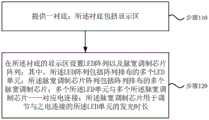
基于同样的发明构思,本发明实施例还提供了一种显示面板的制备方法, 用于制备上述实施例提供的任一显示面板,与上述实施例相同或相应的结构以 及术语的解释在此不再赘述,图31为本发明实施例提供的一种显示面板的制备 方法的流程示意图,如图31所示,该方法包括如下步骤:Based on the same inventive concept, an embodiment of the present invention also provides a method for preparing a display panel, which is used to prepare any display panel provided in the above-mentioned embodiments, and explanations of structures and terms that are the same as or corresponding to the above-mentioned embodiments are here No more details, FIG. 31 is a schematic flow chart of a method for preparing a display panel provided by an embodiment of the present invention. As shown in FIG. 31, the method includes the following steps:

步骤110、提供一衬底;所述衬底包括显示区。Step 110, providing a substrate; the substrate includes a display area.

其中,衬底可以是刚性衬底或柔性衬底,本领域技术人员可根据实际需求 进行设置,本发明实施例对此不作限定。Wherein, the substrate can be a rigid substrate or a flexible substrate, which can be set by those skilled in the art according to actual needs, which is not limited in the embodiment of the present invention.

步骤120、在所述衬底的显示区设置LED阵列以及脉宽调制芯片阵列;其 中,所述LED阵列包括阵列排布的多个LED单元;所述脉宽调制芯片阵列包括 阵列排布的多个脉宽调制芯片;多个所述LED单元与多个所述脉宽调制芯片一 一对应电连接;所述脉宽调制芯片用于调节与之电连接的所述LED单元的发光 时长。Step 120, setting an LED array and a pulse width modulation chip array in the display area of the substrate; wherein, the LED array includes a plurality of LED units arranged in an array; the pulse width modulation chip array includes an array of A plurality of pulse width modulation chips; a plurality of said LED units are electrically connected to a plurality of said pulse width modulation chips one by one;

具体的,每个LED单元对应连接一个脉宽调制芯片,脉宽调制芯片用于调节 与之电连接的LED单元的发光时长,进而通过调节LED单元的发光时长来控制LED单元的显示灰阶。其中,LED单元和脉宽调制芯片可设置在衬底的同一侧,也可设置在衬底的不同侧,本领域技术人员可根据实际需求进行设置。Specifically, each LED unit is correspondingly connected to a pulse width modulation chip, and the pulse width modulation chip is used to adjust the light-emitting duration of the LED unit electrically connected to it, and then control the display gray scale of the LED unit by adjusting the light-emitting time of the LED unit. Wherein, the LED unit and the pulse width modulation chip can be arranged on the same side of the substrate, or on different sides of the substrate, and those skilled in the art can make arrangements according to actual needs.

脉宽调制芯片22位于显示区201,并与LED单元21一一对应设置,脉宽 调制芯片22和与之电连接的LED单元21之间的距离较近,可降低信号延迟, 并且不同脉宽调制芯片22和与其对应的LED单元21之间的距离相同或相当, 从而可减少不同位置处LED单元21的信号差异,有利于提高显示面板的亮度均 一性。The pulsewidth modulation chip 22 is located in thedisplay area 201, and is arranged in one-to-one correspondence with theLED unit 21. The distance between the pulsewidth modulation chip 22 and theLED unit 21 electrically connected to it is relatively close, which can reduce signal delay, and different pulse widths The distance between themodulation chip 22 and thecorresponding LED unit 21 is the same or equivalent, so that the signal difference of theLED unit 21 at different positions can be reduced, which is conducive to improving the brightness uniformity of the display panel.

可选的,在所述衬底的显示区设置LED阵列以及脉宽调制芯片阵列,包括:Optionally, an LED array and a pulse width modulation chip array are set in the display area of the substrate, including:

采用晶圆级工艺制备所述LED阵列,并转印至所述衬底的第一侧。The LED array is prepared by a wafer-level process and transferred to the first side of the substrate.

采用晶圆级工艺制备所述脉宽调制芯片阵列,并转印至所述衬底的第二侧; 其中,所述第一侧和所述第二侧相对。The pulse width modulation chip array is prepared by a wafer-level process, and transferred to the second side of the substrate; wherein, the first side is opposite to the second side.

其中,通过晶圆级工艺,在晶圆上生长LED阵列,与直接在衬底上制备LED 阵列相比,可制备更小的LED单元,有助于提高显示面板的分辨率,在显示面 板应用于透明显示领域中时,LED单元占用的空间更小,提高显示面板的透过 率,改善透明显示的效果。同理,通过晶圆级工艺,在晶圆上生长脉宽调制芯片阵列,可制备更小的脉宽调制芯片,有助于提高显示面板的分辨率,在透明 显示时,提高显示面板的透过率,改善透明显示的效果,此处不再赘述。Among them, through the wafer-level process, the LED array is grown on the wafer. Compared with the LED array directly prepared on the substrate, smaller LED units can be prepared, which helps to improve the resolution of the display panel. In the display panel When applied in the field of transparent display, the space occupied by the LED unit is smaller, the transmittance of the display panel is increased, and the effect of transparent display is improved. In the same way, through the wafer-level process, growing the pulse width modulation chip array on the wafer can prepare smaller pulse width modulation chips, which helps to improve the resolution of the display panel, and improves the transparency of the display panel when it is transparently displayed. Overrate to improve the effect of transparent display, which will not be repeated here.

采用晶圆级工艺制备LED阵列和脉宽调制芯片阵列之后,将LED阵列转印 至衬底的第一侧,将脉宽调制芯片阵列转印至衬底的第二侧,当显示面板应用 于透明显示中时,LED阵列和脉宽调制芯片阵列设置在衬底不同侧,与LED阵 列和脉宽调制芯片阵列均位于衬底的同一侧相比,有助于降低LED阵列和脉宽 调制芯片阵列遮挡衬底的面积,提高显示面板的透过率,实现透明显示。After the LED array and the pulse width modulation chip array are prepared by the wafer level process, the LED array is transferred to the first side of the substrate, and the pulse width modulation chip array is transferred to the second side of the substrate. When the display panel is applied to In transparent display, the LED array and the pulse width modulation chip array are arranged on different sides of the substrate, compared with the LED array and the pulse width modulation chip array being located on the same side of the substrate, it helps to reduce the The chip array blocks the area of the substrate, improves the transmittance of the display panel, and realizes transparent display.

可选的,在所述衬底的显示区设置LED阵列以及脉宽调制芯片阵列包括:Optionally, setting the LED array and the pulse width modulation chip array in the display area of the substrate includes:

通过共晶键合方式将LED阵列的多个LED单元键合在所述衬底的第一侧。A plurality of LED units of the LED array are bonded on the first side of the substrate by eutectic bonding.

通过共晶键合方式将脉宽调制芯片阵列的多个脉宽调制芯片键合在所述衬 底的第二侧。A plurality of pulse width modulation chips of the pulse width modulation chip array are bonded on the second side of the substrate by eutectic bonding.

示例性的,图32为本发明实施例提供的另一种显示面板的制备方法的流程 示意图,如图32所示,以恒流开关单元(图中未示出)位于衬底基板201背离 脉宽调制芯片(图中未示出)的一侧为例,在衬底基板201一侧制备恒流开关 单元之后,形成衬底20,衬底20包括引出电极91,引出电极91用于将LED单 元与脉宽调制芯片或其他驱动电路电连接,其中,引出电极91可以为ITO或其 他导电材料,本发明实施例对此不作限定。Exemplarily, FIG. 32 is a schematic flowchart of another method for manufacturing a display panel provided by an embodiment of the present invention. As shown in FIG. One side of the width modulation chip (not shown in the figure) is taken as an example. After the constant current switch unit is prepared on the side of thesubstrate substrate 201, thesubstrate 20 is formed. Thesubstrate 20 includes the lead-out electrode 91, which is used to connect the LED The unit is electrically connected to a pulse width modulation chip or other driving circuits, wherein the lead-out electrode 91 can be made of ITO or other conductive materials, which is not limited in this embodiment of the present invention.

在衬底20上涂覆一层负性光阻层92,通过光刻工艺对负性光阻层92进行 光刻,从而暴露出引出电极91,再蒸镀一层共晶层93,随后利用NPR剥离技术 去除负性光阻层92,从而实现在引出电极91远离衬底20的一侧制备共晶层93。 利用共晶焊接设备将LED单元21键合到共晶层93,从而通过共晶键合方式实现LED单元21与衬底20之间的电连接。同理,通过共晶键合方式将脉宽调制 芯片阵列的多个脉宽调制芯片(图中未示出)键合在衬底20的第二侧,从而完 成显示面板的制备。A layer ofnegative photoresist layer 92 is coated on thesubstrate 20, and thenegative photoresist layer 92 is photoetched by a photolithography process, thereby exposing theextraction electrode 91, and then a layer ofeutectic layer 93 is evaporated, and then used The NPR lift-off technique removes thenegative photoresist layer 92, thereby realizing the preparation of theeutectic layer 93 on the side of the lead-out electrode 91 away from thesubstrate 20. TheLED unit 21 is bonded to theeutectic layer 93 by eutectic bonding equipment, so as to realize the electrical connection between theLED unit 21 and thesubstrate 20 through eutectic bonding. Similarly, multiple pulse width modulation chips (not shown in the figure) of the pulse width modulation chip array are bonded to the second side of thesubstrate 20 by eutectic bonding, thereby completing the preparation of the display panel.

本发明实施例提供的显示面板的制备方法,通过采用晶圆级工艺制备LED 阵列和脉宽调制芯片阵列,可制备更小的LED单元和脉宽调制芯片,有助于提 高显示面板的分辨率,在显示面板应用于透明显示领域中时,LED单元和脉宽 调制芯片占用的空间更小,提高显示面板的透过率,改善透明显示的效果。同 时,通过将LED阵列和脉宽调制芯片阵列转印至衬底的不同侧,与LED阵列和脉宽调制芯片阵列均位于衬底的同一侧相比,有助于降低LED阵列和脉宽调制 芯片阵列遮挡衬底的面积,提高显示面板的透过率,有助于实现透明显示。The preparation method of the display panel provided by the embodiment of the present invention can prepare smaller LED units and pulse width modulation chips by using a wafer-level process to prepare an LED array and a pulse width modulation chip array, which helps to improve the resolution of the display panel. When the display panel is used in the field of transparent display, the space occupied by the LED unit and the pulse width modulation chip is smaller, the transmittance of the display panel is improved, and the effect of transparent display is improved. At the same time, by transferring the LED array and the pulse width modulation chip array to different sides of the substrate, compared with the LED array and the pulse width modulation chip array being located on the same side of the substrate, it helps to reduce the LED array and pulse width. The modulation chip array blocks the area of the substrate, improves the transmittance of the display panel, and helps realize transparent display.

注意,上述仅为本发明的较佳实施例及所运用技术原理。本领域技术人员 会理解,本发明不限于这里所述的特定实施例,对本领域技术人员来说能够进 行各种明显的变化、重新调整和替代而不会脱离本发明的保护范围。因此,虽 然通过以上实施例对本发明进行了较为详细的说明,但是本发明不仅仅限于以 上实施例,在不脱离本发明构思的情况下,还可以包括更多其他等效实施例,而本发明的范围由所附的权利要求范围决定。Note that the above are only preferred embodiments of the present invention and applied technical principles. Those skilled in the art will understand that the present invention is not limited to the specific embodiments described here, and various obvious changes, readjustments and substitutions can be made by those skilled in the art without departing from the protection scope of the present invention. Therefore, although the present invention has been described in more detail through the above embodiments, the present invention is not limited to the above embodiments, and can also include more other equivalent embodiments without departing from the concept of the present invention. The scope of the present invention is determined by the appended claims.

Claims (27)

Translated fromChinese
1.一种显示面板,其特征在于,包括:1. A display panel, characterized in that, comprising:衬底,所述衬底包括显示区;a substrate comprising a display region;位于所述显示区的LED阵列;所述LED阵列包括阵列排布的多个LED单元;An LED array located in the display area; the LED array includes a plurality of LED units arranged in an array;位于所述显示区的脉宽调制芯片阵列;所述脉宽调制芯片阵列包括阵列排布的多个脉宽调制芯片;A pulse width modulation chip array located in the display area; the pulse width modulation chip array includes a plurality of pulse width modulation chips arranged in an array;多个所述LED单元与多个所述脉宽调制芯片一一对应电连接;所述脉宽调制芯片用于调节与之电连接的所述LED单元的发光时长;A plurality of the LED units are electrically connected to a plurality of the pulse width modulation chips in one-to-one correspondence; the pulse width modulation chips are used to adjust the light-emitting duration of the LED units electrically connected thereto;所述脉宽调制芯片包括数据信号端、扫描信号端、恒流电源输入端以及输出端;所述脉宽调制芯片的输出端与所述LED单元电连接;所述脉宽调制芯片用于在所述扫描信号端输入有效扫描脉冲时启动,并根据所述数据信号端输入的数据信号,调节与之电连接的所述LED单元的发光时长;所述脉宽调制芯片包括:脉宽调制单元、恒流单元和开关单元;所述脉宽调制单元包括所述数据信号端和所述扫描信号端;所述恒流单元包括所述恒流电源输入端;所述恒流单元的输出端与所述开关单元的第一端电连接;所述恒流单元用于向所述开关单元输入恒定驱动电流;所述开关单元的控制端与所述脉宽调制单元的输出端电连接;所述开关单元的第二端为所述脉宽调制芯片的输出端;所述脉宽调制单元用于在所述扫描信号端输入有效扫描脉冲时启动,并根据所述数据信号端输入的数据信号,调节输出脉冲信号的脉宽;所述开关单元用于根据所述脉冲信号控制所述LED单元的发光时长;The pulse width modulation chip includes a data signal terminal, a scanning signal terminal, a constant current power supply input terminal and an output terminal; the output terminal of the pulse width modulation chip is electrically connected to the LED unit; the pulse width modulation chip is used for The scan signal end starts when an effective scan pulse is input, and adjusts the light-emitting duration of the LED unit electrically connected to it according to the data signal input by the data signal end; the pulse width modulation chip includes: a pulse width modulation unit , a constant current unit and a switch unit; the pulse width modulation unit includes the data signal end and the scanning signal end; the constant current unit includes the input end of the constant current power supply; the output end of the constant current unit is connected to the The first terminal of the switch unit is electrically connected; the constant current unit is used to input a constant driving current to the switch unit; the control terminal of the switch unit is electrically connected to the output terminal of the pulse width modulation unit; the The second end of the switch unit is the output end of the pulse width modulation chip; the pulse width modulation unit is used to start when an effective scan pulse is input at the scan signal end, and according to the data signal input at the data signal end, Adjusting the pulse width of the output pulse signal; the switch unit is used to control the light-emitting duration of the LED unit according to the pulse signal;或者,or,所述衬底包括衬底基板和位于所述衬底基板一侧的多个恒流开关单元;多个恒流开关单元与多个所述脉宽调制芯片一一对应;所述恒流开关单元包括恒流单元和开关单元;所述脉宽调制芯片通过所述恒流开关单元与所述LED单元电连接;所述脉宽调制芯片包括数据信号端、扫描信号端以及输出端;所述脉宽调制芯片的输出端与所述开关单元的控制端电连接;所述开关单元的第一端与所述恒流单元的输出端电连接;所述恒流单元包括恒流电源输入端;所述恒流单元用于向所述开关单元输入恒定驱动电流;所述开关单元的第二端与所述LED单元电连接;所述脉宽调制芯片用于在所述扫描信号端输入有效扫描脉冲时启动,并根据所述数据信号端输入的数据信号,调节向与之电连接的所述开关单元输出的脉冲信号的脉宽,以使所述开关单元根据所述脉冲信号控制所述LED单元的发光时长。The substrate includes a substrate substrate and a plurality of constant current switch units located on one side of the substrate substrate; the plurality of constant current switch units correspond to the plurality of pulse width modulation chips; the constant current switch unit It includes a constant current unit and a switch unit; the pulse width modulation chip is electrically connected to the LED unit through the constant current switch unit; the pulse width modulation chip includes a data signal terminal, a scanning signal terminal and an output terminal; the pulse width modulation chip The output end of the wide modulation chip is electrically connected to the control end of the switch unit; the first end of the switch unit is electrically connected to the output end of the constant current unit; the constant current unit includes a constant current power supply input end; the The constant current unit is used to input a constant driving current to the switch unit; the second end of the switch unit is electrically connected to the LED unit; the pulse width modulation chip is used to input an effective scan pulse at the scan signal terminal start at time, and adjust the pulse width of the pulse signal output to the switch unit electrically connected to it according to the data signal input from the data signal terminal, so that the switch unit controls the LED unit according to the pulse signal of luminous duration.2.根据权利要求1所述的显示面板,其特征在于,各所述LED单元的驱动电流的电流值相同。2. The display panel according to claim 1, wherein the driving currents of the LED units have the same current value.3.根据权利要求1所述的显示面板,其特征在于,所述衬底还包括非显示区;3. The display panel according to claim 1, wherein the substrate further comprises a non-display area;所述显示面板还包括:The display panel also includes:位于所述非显示区的驱动芯片;a driver chip located in the non-display area;多条数据线和多条扫描线;Multiple data lines and multiple scan lines;所述驱动芯片用于通过所述扫描线向所述脉宽调制芯片提供扫描信号;所述驱动芯片用于通过所述数据线向所述脉宽调制芯片提供数据信号。The driving chip is used to provide scanning signals to the pulse width modulation chip through the scanning lines; the driving chip is used to provide data signals to the pulse width modulation chip through the data lines.4.根据权利要求1所述的显示面板,其特征在于,所述衬底包括相对的第一侧和第二侧;所述LED阵列位于所述第一侧;所述脉宽调制芯片阵列位于所述第二侧;所述衬底采用透明材料。4. The display panel according to claim 1, wherein the substrate comprises opposite first sides and second sides; the LED array is located on the first side; the pulse width modulation chip array is located on The second side; the substrate is made of transparent material.5.根据权利要求4所述的显示面板,其特征在于,在垂直于所述衬底的方向,一一对应电连接的所述LED单元与所述脉宽调制芯片交叠。5 . The display panel according to claim 4 , wherein, in a direction perpendicular to the substrate, the LED units that are electrically connected in one-to-one correspondence overlap with the pulse width modulation chip.6.根据权利要求4所述的显示面板,其特征在于,所述衬底的第一侧设置有相互绝缘的多条数据线和多条扫描线;6. The display panel according to claim 4, wherein a plurality of data lines and a plurality of scan lines insulated from each other are provided on the first side of the substrate;所述衬底设置有多个第一过孔、多个第二过孔以及多个第三过孔;所述扫描线通过所述第一过孔与所述脉宽调制芯片电连接;所述数据线通过所述第二过孔与所述脉宽调制芯片电连接;所述脉宽调制芯片通过所述第三过孔与所述LED单元电连接。The substrate is provided with a plurality of first via holes, a plurality of second via holes and a plurality of third via holes; the scanning line is electrically connected to the pulse width modulation chip through the first via holes; the The data line is electrically connected to the pulse width modulation chip through the second via hole; the pulse width modulation chip is electrically connected to the LED unit through the third via hole.7.根据权利要求4所述的显示面板,其特征在于,所述衬底的第二侧设置有多条数据线和多条扫描线;所述数据线以及所述扫描线在所述第二侧与所述脉宽调制芯片电连接;所述衬底设置有多个第三过孔;所述脉宽调制芯片通过所述第三过孔与所述LED单元电连接。7. The display panel according to claim 4, wherein a plurality of data lines and a plurality of scan lines are arranged on the second side of the substrate; the data lines and the scan lines are arranged on the second side The side is electrically connected to the pulse width modulation chip; the substrate is provided with a plurality of third via holes; the pulse width modulation chip is electrically connected to the LED unit through the third via holes.8.根据权利要求1所述的显示面板,其特征在于,所述开关单元包括开关晶体管;所述开关晶体管的第一极与所述恒流单元的输出端电连接;所述开关晶体管的第二极与所述LED单元电连接。8. The display panel according to claim 1, wherein the switch unit comprises a switch transistor; the first pole of the switch transistor is electrically connected to the output terminal of the constant current unit; the second pole of the switch transistor The diode is electrically connected with the LED unit.9.根据权利要求1所述的显示面板,其特征在于,所述脉宽调制芯片包括寄存器和状态机;9. The display panel according to claim 1, wherein the pulse width modulation chip comprises a register and a state machine;所述寄存器与所述数据信号端电连接;所述状态机分别与所述扫描信号端、所述寄存器以及所述开关单元电连接;The register is electrically connected to the data signal terminal; the state machine is electrically connected to the scan signal terminal, the register and the switch unit respectively;所述状态机用于根据所述扫描信号端输入的扫描信号控制所述状态机启动或关闭;所述寄存器用于存储所述数据信号端输入的数据信号;The state machine is used to control the startup or shutdown of the state machine according to the scanning signal input from the scanning signal terminal; the register is used to store the data signal input from the data signal terminal;所述状态机还用于根据所述扫描信号端输入的扫描信号以及从所述寄存器中读取的数据信号调节输出脉冲信号的脉宽。The state machine is also used to adjust the pulse width of the output pulse signal according to the scan signal input from the scan signal terminal and the data signal read from the register.10.根据权利要求1所述的显示面板,其特征在于,所述衬底上还设置有多条正性电源信号线,所述正性电源信号线与所述恒流电源输入端电连接;所述正性电源信号线与所述脉宽调制芯片位于所述衬底的同一侧。10. The display panel according to claim 1, wherein the substrate is further provided with a plurality of positive power signal lines, and the positive power signal lines are electrically connected to the input terminal of the constant current power supply; The positive power signal line and the pulse width modulation chip are located on the same side of the substrate.11.根据权利要求1所述的显示面板,其特征在于,所述衬底上还设置有多条正性电源信号线;所述衬底还包括多个第四过孔,所述正性电源信号线与所述脉宽调制芯片位于所述衬底的不同侧;所述正性电源信号线通过所述第四过孔与所述恒流电源输入端电连接。11. The display panel according to claim 1, wherein the substrate is further provided with a plurality of positive power supply signal lines; the substrate further comprises a plurality of fourth via holes, and the positive power supply The signal line and the pulse width modulation chip are located on different sides of the substrate; the positive power signal line is electrically connected to the input end of the constant current power supply through the fourth via hole.12.根据权利要求1所述的显示面板,其特征在于,所述衬底上还设置有多条正性电源信号线,所述正性电源信号线与所述恒流开关单元位于所述衬底基板的同一侧。12. The display panel according to claim 1, wherein a plurality of positive power signal lines are arranged on the substrate, and the positive power signal lines and the constant current switch unit are located on the substrate. same side of the base substrate.13.根据权利要求1所述的显示面板,其特征在于,所述衬底上还设置有多条正性电源信号线,所述衬底还包括多个第五过孔,所述正性电源信号线与所述恒流开关单元位于所述衬底基板的不同侧;所述正性电源信号线通过所述第五过孔与所述恒流电源输入端电连接。13. The display panel according to claim 1, wherein a plurality of positive power supply signal lines are arranged on the substrate, and the substrate further includes a plurality of fifth via holes, and the positive power supply The signal line and the constant current switch unit are located on different sides of the substrate; the positive power signal line is electrically connected to the input end of the constant current power supply through the fifth via hole.14.根据权利要求1所述的显示面板,其特征在于,所述衬底上还设置有多条负性电源信号线,各所述LED单元与所述负性电源信号线电连接。14. The display panel according to claim 1, wherein a plurality of negative power signal lines are arranged on the substrate, and each of the LED units is electrically connected to the negative power signal lines.15.根据权利要求14所述的显示面板,其特征在于,所述负性电源信号线与所述LED单元位于所述衬底的同一侧。15. The display panel according to claim 14, wherein the negative power signal line and the LED unit are located on the same side of the substrate.16.根据权利要求14所述的显示面板,其特征在于,所述负性电源信号线与所述LED单元位于所述衬底的不同侧;所述衬底包括多个第六过孔;所述负性电源信号线通过所述第六过孔与所述LED单元电连接。16. The display panel according to claim 14, wherein the negative power signal line and the LED unit are located on different sides of the substrate; the substrate includes a plurality of sixth via holes; The negative power signal line is electrically connected to the LED unit through the sixth via hole.17.根据权利要求1所述的显示面板,其特征在于,所述显示面板包括阵列排布的多个子像素;每个所述子像素包括一所述LED单元和一所述脉宽调制芯片;每个所述LED单元包括N个LED子单元;同一所述子像素中的N个所述LED子单元分别与该所述子像素的所述脉宽调制芯片电连接;N为大于1的正整数。17. The display panel according to claim 1, wherein the display panel comprises a plurality of sub-pixels arranged in an array; each of the sub-pixels comprises a LED unit and a pulse width modulation chip; Each of the LED units includes N LED subunits; the N LED subunits in the same subpixel are respectively electrically connected to the pulse width modulation chip of the subpixel; N is a positive value greater than 1. integer.18.根据权利要求17所述的显示面板,其特征在于,所述显示面板还包括多条数据线和多条扫描线;18. The display panel according to claim 17, further comprising a plurality of data lines and a plurality of scan lines;每个所述子像素的所述脉宽调制芯片与N条所述数据线电连接;同一行所述子像素的所述脉宽调制芯片与同一所述扫描线电连接;不同行所述子像素的所述脉宽调制芯片连接不同所述扫描线。The pulse width modulation chip of each sub-pixel is electrically connected to N data lines; the pulse width modulation chip of the same row of sub-pixels is electrically connected to the same scanning line; The pulse width modulation chips of the pixels are connected to different scan lines.19.根据权利要求17所述的显示面板,其特征在于,所述显示面板还包括多条数据线和多条扫描线;19. The display panel according to claim 17, further comprising a plurality of data lines and a plurality of scan lines;同一列所述子像素的所述脉宽调制芯片与同一所述数据线电连接;不同列所述子像素的所述脉宽调制芯片连接不同所述数据线;每个所述子像素的所述脉宽调制芯片与N条所述扫描线电连接。The pulse width modulation chips of the sub-pixels in the same column are electrically connected to the same data line; the pulse width modulation chips of the sub-pixels in different columns are connected to different data lines; The pulse width modulation chip is electrically connected to the N scanning lines.20.根据权利要求1所述的显示面板,其特征在于,所述显示面板包括阵列排布的多个子像素;每个所述子像素包括一所述LED单元和一所述脉宽调制芯片;每个所述LED单元包括N个LED子单元;每个所述脉宽调制芯片包括N个脉宽调制子芯片;同一所述子像素中的N个所述LED子单元分别与该所述子像素的N个所述脉宽调制子芯片一一对应电连接;N为大于1的正整数。20. The display panel according to claim 1, wherein the display panel comprises a plurality of sub-pixels arranged in an array; each of the sub-pixels comprises a LED unit and a pulse width modulation chip; Each of the LED units includes N LED sub-units; each of the pulse width modulation chips includes N pulse width modulation sub-chips; the N LED sub-units in the same sub-pixel are respectively connected to the sub- The N pulse width modulation sub-chips of the pixel are electrically connected in one-to-one correspondence; N is a positive integer greater than 1.21.根据权利要求20所述的显示面板,其特征在于,所述显示面板还包括多条数据线和多条扫描线;21. The display panel according to claim 20, further comprising a plurality of data lines and a plurality of scan lines;每个所述子像素的N个所述脉宽调制子芯片与N条所述数据线一一对应电连接;每个所述子像素的N个所述脉宽调制子芯片连接同一所述扫描线。The N pulse width modulation sub-chips of each sub-pixel are electrically connected to the N data lines in one-to-one correspondence; the N pulse width modulation sub-chips of each sub-pixel are connected to the same scanning Wire.22.根据权利要求20所述的显示面板,其特征在于,所述显示面板还包括多条数据线和多条扫描线;22. The display panel according to claim 20, further comprising a plurality of data lines and a plurality of scan lines;每个所述子像素的N个所述脉宽调制子芯片与N条所述扫描线一一对应电连接;每个所述子像素的N个所述脉宽调制子芯片连接同一所述数据线。The N pulse width modulation sub-chips of each sub-pixel are electrically connected to the N scanning lines in one-to-one correspondence; the N pulse width modulation sub-chips of each sub-pixel are connected to the same data Wire.23.根据权利要求20所述的显示面板,其特征在于,所述显示面板还包括多条数据线和多条扫描线;23. The display panel according to claim 20, further comprising a plurality of data lines and a plurality of scan lines;每个所述子像素的N个所述脉宽调制子芯片与N条所述数据线一一对应电连接;每个所述子像素的N个所述脉宽调制子芯片与N条所述扫描线一一对应电连接。The N pulse width modulation sub-chips of each sub-pixel are electrically connected to the N data lines in one-to-one correspondence; the N pulse width modulation sub-chips of each sub-pixel are connected to the N said data lines. The scan lines are electrically connected in one-to-one correspondence.24.一种显示装置,其特征在于,包括权利要求1-23中任一项所述的显示面板。24. A display device, comprising the display panel according to any one of claims 1-23.25.一种显示面板的制备方法,其特征在于,包括:25. A method for preparing a display panel, comprising:提供一衬底;所述衬底包括显示区;A substrate is provided; the substrate includes a display area;在所述衬底的显示区设置LED阵列以及脉宽调制芯片阵列;An LED array and a pulse width modulation chip array are arranged in the display area of the substrate;其中,所述LED阵列包括阵列排布的多个LED单元;所述脉宽调制芯片阵列包括阵列排布的多个脉宽调制芯片;多个所述LED单元与多个所述脉宽调制芯片一一对应电连接;所述脉宽调制芯片用于调节与之电连接的所述LED单元的发光时长;Wherein, the LED array includes a plurality of LED units arranged in an array; the pulse width modulation chip array includes a plurality of pulse width modulation chips arranged in an array; a plurality of the LED units and a plurality of the pulse width modulation chips One-to-one electrical connection; the pulse width modulation chip is used to adjust the light-emitting duration of the LED unit electrically connected to it;所述脉宽调制芯片包括数据信号端、扫描信号端、恒流电源输入端以及输出端;所述脉宽调制芯片的输出端与所述LED单元电连接;所述脉宽调制芯片用于在所述扫描信号端输入有效扫描脉冲时启动,并根据所述数据信号端输入的数据信号,调节与之电连接的所述LED单元的发光时长;所述脉宽调制芯片包括:脉宽调制单元、恒流单元和开关单元;所述脉宽调制单元包括所述数据信号端和所述扫描信号端;所述恒流单元包括所述恒流电源输入端;所述恒流单元的输出端与所述开关单元的第一端电连接;所述恒流单元用于向所述开关单元输入恒定驱动电流;所述开关单元的控制端与所述脉宽调制单元的输出端电连接;所述开关单元的第二端为所述脉宽调制芯片的输出端;所述脉宽调制单元用于在所述扫描信号端输入有效扫描脉冲时启动,并根据所述数据信号端输入的数据信号,调节输出脉冲信号的脉宽;所述开关单元用于根据所述脉冲信号控制所述LED单元的发光时长;The pulse width modulation chip includes a data signal terminal, a scanning signal terminal, a constant current power supply input terminal and an output terminal; the output terminal of the pulse width modulation chip is electrically connected to the LED unit; the pulse width modulation chip is used for The scan signal end starts when an effective scan pulse is input, and adjusts the light-emitting duration of the LED unit electrically connected to it according to the data signal input by the data signal end; the pulse width modulation chip includes: a pulse width modulation unit , a constant current unit and a switch unit; the pulse width modulation unit includes the data signal end and the scanning signal end; the constant current unit includes the input end of the constant current power supply; the output end of the constant current unit is connected to the The first terminal of the switch unit is electrically connected; the constant current unit is used to input a constant driving current to the switch unit; the control terminal of the switch unit is electrically connected to the output terminal of the pulse width modulation unit; the The second end of the switch unit is the output end of the pulse width modulation chip; the pulse width modulation unit is used to start when an effective scan pulse is input at the scan signal end, and according to the data signal input at the data signal end, Adjusting the pulse width of the output pulse signal; the switch unit is used to control the light-emitting duration of the LED unit according to the pulse signal;或者,or,所述衬底包括衬底基板和位于所述衬底基板一侧的多个恒流开关单元;多个恒流开关单元与多个所述脉宽调制芯片一一对应;所述恒流开关单元包括恒流单元和开关单元;所述脉宽调制芯片通过所述恒流开关单元与所述LED单元电连接;所述脉宽调制芯片包括数据信号端、扫描信号端以及输出端;所述脉宽调制芯片的输出端与所述开关单元的控制端电连接;所述开关单元的第一端与所述恒流单元的输出端电连接;所述恒流单元包括恒流电源输入端;所述恒流单元用于向所述开关单元输入恒定驱动电流;所述开关单元的第二端与所述LED单元电连接;所述脉宽调制芯片用于在所述扫描信号端输入有效扫描脉冲时启动,并根据所述数据信号端输入的数据信号,调节向与之电连接的所述开关单元输出的脉冲信号的脉宽,以使所述开关单元根据所述脉冲信号控制所述LED单元的发光时长。The substrate includes a substrate substrate and a plurality of constant current switch units located on one side of the substrate substrate; the plurality of constant current switch units correspond to the plurality of pulse width modulation chips; the constant current switch unit It includes a constant current unit and a switch unit; the pulse width modulation chip is electrically connected to the LED unit through the constant current switch unit; the pulse width modulation chip includes a data signal terminal, a scanning signal terminal and an output terminal; the pulse width modulation chip The output end of the wide modulation chip is electrically connected to the control end of the switch unit; the first end of the switch unit is electrically connected to the output end of the constant current unit; the constant current unit includes a constant current power supply input end; the The constant current unit is used to input a constant driving current to the switch unit; the second end of the switch unit is electrically connected to the LED unit; the pulse width modulation chip is used to input an effective scan pulse at the scan signal terminal start at time, and adjust the pulse width of the pulse signal output to the switch unit electrically connected to it according to the data signal input from the data signal terminal, so that the switch unit controls the LED unit according to the pulse signal of luminous duration.26.根据权利要求25所述的方法,其特征在于,在所述衬底的显示区设置LED阵列以及脉宽调制芯片阵列,包括:26. The method according to claim 25, wherein an LED array and a pulse width modulation chip array are arranged in the display area of the substrate, comprising:采用晶圆级工艺制备所述LED阵列,并转印至所述衬底的第一侧;preparing the LED array by using a wafer-level process, and transferring it to the first side of the substrate;采用晶圆级工艺制备所述脉宽调制芯片阵列,并转印至所述衬底的第二侧;preparing the pulse width modulation chip array by wafer-level process, and transferring to the second side of the substrate;其中,所述第一侧和所述第二侧相对。Wherein, the first side is opposite to the second side.27.根据权利要求25所述的方法,其特征在于,在所述衬底的显示区设置LED阵列以及脉宽调制芯片阵列包括:27. The method according to claim 25, wherein arranging the LED array and the pulse width modulation chip array in the display area of the substrate comprises:通过共晶键合方式将LED阵列的多个LED单元键合在所述衬底的第一侧;bonding a plurality of LED units of the LED array on the first side of the substrate by eutectic bonding;通过共晶键合方式将脉宽调制芯片阵列的多个脉宽调制芯片键合在所述衬底的第二侧。A plurality of pulse width modulation chips of the pulse width modulation chip array are bonded on the second side of the substrate by eutectic bonding.
CN202011386324.5A2020-12-012020-12-01 Display panel, manufacturing method thereof, and display deviceActiveCN112669761B (en)

Priority Applications (2)

Application NumberPriority DateFiling DateTitle
CN202011386324.5ACN112669761B (en)2020-12-012020-12-01 Display panel, manufacturing method thereof, and display device
US17/159,777US12087747B2 (en)2020-12-012021-01-27Display panel and fabrication method thereof, and display device

Applications Claiming Priority (1)

Application NumberPriority DateFiling DateTitle
CN202011386324.5ACN112669761B (en)2020-12-012020-12-01 Display panel, manufacturing method thereof, and display device

Publications (2)

Publication NumberPublication Date
CN112669761A CN112669761A (en)2021-04-16
CN112669761Btrue CN112669761B (en)2023-05-05

Family

ID=75400759

Family Applications (1)

Application NumberTitlePriority DateFiling Date
CN202011386324.5AActiveCN112669761B (en)2020-12-012020-12-01 Display panel, manufacturing method thereof, and display device

Country Status (2)

CountryLink
US (1)US12087747B2 (en)
CN (1)CN112669761B (en)

Families Citing this family (3)

* Cited by examiner, † Cited by third party
Publication numberPriority datePublication dateAssigneeTitle
CN111682044B (en)*2020-07-102022-04-08深圳市华星光电半导体显示技术有限公司 A display panel, method for producing the same, and display device
CN114141937B (en)*2021-11-162024-01-09Tcl华星光电技术有限公司Backlight plate and display panel
CN117636801A (en)*2023-11-282024-03-01维沃移动通信有限公司 Display control method and electronic device

Family Cites Families (15)

* Cited by examiner, † Cited by third party
Publication numberPriority datePublication dateAssigneeTitle
EP2668828A4 (en)*2011-01-282016-09-28Seoul Semiconductor Co LtdLed driving circuit package
TWI519879B (en)*2013-11-082016-02-01群創光電股份有限公司 Display panel and display device including the same
TW201629937A (en)*2015-02-132016-08-16廣東威創視訊科技股份有限公司Light emitting diode display
US10832609B2 (en)*2017-01-102020-11-10X Display Company Technology LimitedDigital-drive pulse-width-modulated output system
US11189605B2 (en)2018-02-282021-11-30X Display Company Technology LimitedDisplays with transparent bezels
CN110556072B (en)*2018-05-312024-07-02三星电子株式会社 Display panel and method for driving the same
KR102033108B1 (en)*2018-07-062019-10-16엘지전자 주식회사Display apparatus and driving method thereof
CN109345963B (en)*2018-10-122020-12-18芯光科技新加坡有限公司 A display device and packaging method thereof
CN109768027B (en)2019-01-292020-07-07福州大学Structure and manufacturing method of Micro-LED display screen
CN110085164B (en)*2019-05-292020-11-10深圳市华星光电半导体显示技术有限公司Display panel and display device
US20210183833A1 (en)*2019-12-172021-06-17Innolux CorporationElectronic device
US20210257348A1 (en)*2020-02-132021-08-19Tek Beng LowLight emitting diode package having back-to-back compartment configuration
CN111681598A (en)*2020-06-032020-09-18深圳市华星光电半导体显示技术有限公司 Display panel and manufacturing method thereof
CN113805378B (en)*2020-06-122022-07-26京东方科技集团股份有限公司 Light-emitting substrate and display device
CN113724653B (en)*2021-08-302023-04-18京东方科技集团股份有限公司Display adjusting circuit, method and display device

Also Published As

Publication numberPublication date
US12087747B2 (en)2024-09-10
US20220173087A1 (en)2022-06-02
CN112669761A (en)2021-04-16

Similar Documents

PublicationPublication DateTitle
CN113409727B (en)Pixel driving circuit, display panel, control method of display panel and display device
CN112669761B (en) Display panel, manufacturing method thereof, and display device
KR20250102115A (en)Array substrate, display panel, tiled display panel and display driving method
US10839756B2 (en)Micro display device and display integrated circuit having dual chips stacked with each other
US12073762B2 (en)Pixel driving circuit, pixel driving method, display panel and display device
US20220415873A1 (en)Display module and display apparatus having the same
US20220278260A1 (en)Display apparatus using semiconductor light emitting device
WO2021035414A1 (en)Pixel circuit and driving method therefor, and display substrate and driving method therefor, and display device
US12278225B2 (en)Display module, display apparatus, and method of manufacturing the same
US12132037B2 (en)Display apparatus
CN115273744A (en)Display module and display device
CN113811938B (en)Display substrate and testing method thereof
US12205977B2 (en)Display module, display apparatus and method for manufacturing the same
CN117198212A (en)Display panel
CN111682043B (en) Chip structure, manufacturing method thereof, and display device
CN112740421B (en) Display device and method for manufacturing the same
CN114902408A (en) LED display device and manufacturing method thereof
WO2022110015A1 (en)Display substrate, display panel, and display device
KR102640035B1 (en) display device
US20230387144A1 (en)Display module, display apparatus and method for manufacturing same
CN114446240B (en) Display panel power supply circuit, display panel and display device
KR20230153891A (en)Transparent display module and transparent display apparatus
CN114694590B (en)Display device and method for manufacturing the same
US12119333B2 (en)Display apparatus using semiconductor light-emitting device
CN112703604B (en)Display device and method for manufacturing the same

Legal Events

DateCodeTitleDescription
PB01Publication
PB01Publication
SE01Entry into force of request for substantive examination
GR01Patent grant
GR01Patent grant

[8]ページ先頭

©2009-2025 Movatter.jp