CN112585293B - Device and method for producing layers in a coating system - Google Patents
Device and method for producing layers in a coating systemDownload PDFInfo
- Publication number
- CN112585293B CN112585293BCN201980052966.0ACN201980052966ACN112585293BCN 112585293 BCN112585293 BCN 112585293BCN 201980052966 ACN201980052966 ACN 201980052966ACN 112585293 BCN112585293 BCN 112585293B
- Authority
- CN
- China
- Prior art keywords
- magnetron
- substrate
- source
- layer
- turntable
- Prior art date
- Legal status (The legal status is an assumption and is not a legal conclusion. Google has not performed a legal analysis and makes no representation as to the accuracy of the status listed.)
- Active
Links
Images


Classifications
- C—CHEMISTRY; METALLURGY
- C23—COATING METALLIC MATERIAL; COATING MATERIAL WITH METALLIC MATERIAL; CHEMICAL SURFACE TREATMENT; DIFFUSION TREATMENT OF METALLIC MATERIAL; COATING BY VACUUM EVAPORATION, BY SPUTTERING, BY ION IMPLANTATION OR BY CHEMICAL VAPOUR DEPOSITION, IN GENERAL; INHIBITING CORROSION OF METALLIC MATERIAL OR INCRUSTATION IN GENERAL
- C23C—COATING METALLIC MATERIAL; COATING MATERIAL WITH METALLIC MATERIAL; SURFACE TREATMENT OF METALLIC MATERIAL BY DIFFUSION INTO THE SURFACE, BY CHEMICAL CONVERSION OR SUBSTITUTION; COATING BY VACUUM EVAPORATION, BY SPUTTERING, BY ION IMPLANTATION OR BY CHEMICAL VAPOUR DEPOSITION, IN GENERAL
- C23C14/00—Coating by vacuum evaporation, by sputtering or by ion implantation of the coating forming material
- C23C14/04—Coating on selected surface areas, e.g. using masks
- C23C14/042—Coating on selected surface areas, e.g. using masks using masks
- C23C14/044—Coating on selected surface areas, e.g. using masks using masks using masks to redistribute rather than totally prevent coating, e.g. producing thickness gradient
- C—CHEMISTRY; METALLURGY
- C23—COATING METALLIC MATERIAL; COATING MATERIAL WITH METALLIC MATERIAL; CHEMICAL SURFACE TREATMENT; DIFFUSION TREATMENT OF METALLIC MATERIAL; COATING BY VACUUM EVAPORATION, BY SPUTTERING, BY ION IMPLANTATION OR BY CHEMICAL VAPOUR DEPOSITION, IN GENERAL; INHIBITING CORROSION OF METALLIC MATERIAL OR INCRUSTATION IN GENERAL
- C23C—COATING METALLIC MATERIAL; COATING MATERIAL WITH METALLIC MATERIAL; SURFACE TREATMENT OF METALLIC MATERIAL BY DIFFUSION INTO THE SURFACE, BY CHEMICAL CONVERSION OR SUBSTITUTION; COATING BY VACUUM EVAPORATION, BY SPUTTERING, BY ION IMPLANTATION OR BY CHEMICAL VAPOUR DEPOSITION, IN GENERAL
- C23C14/00—Coating by vacuum evaporation, by sputtering or by ion implantation of the coating forming material
- C23C14/22—Coating by vacuum evaporation, by sputtering or by ion implantation of the coating forming material characterised by the process of coating
- C23C14/34—Sputtering
- C23C14/3485—Sputtering using pulsed power to the target
- C—CHEMISTRY; METALLURGY
- C23—COATING METALLIC MATERIAL; COATING MATERIAL WITH METALLIC MATERIAL; CHEMICAL SURFACE TREATMENT; DIFFUSION TREATMENT OF METALLIC MATERIAL; COATING BY VACUUM EVAPORATION, BY SPUTTERING, BY ION IMPLANTATION OR BY CHEMICAL VAPOUR DEPOSITION, IN GENERAL; INHIBITING CORROSION OF METALLIC MATERIAL OR INCRUSTATION IN GENERAL
- C23C—COATING METALLIC MATERIAL; COATING MATERIAL WITH METALLIC MATERIAL; SURFACE TREATMENT OF METALLIC MATERIAL BY DIFFUSION INTO THE SURFACE, BY CHEMICAL CONVERSION OR SUBSTITUTION; COATING BY VACUUM EVAPORATION, BY SPUTTERING, BY ION IMPLANTATION OR BY CHEMICAL VAPOUR DEPOSITION, IN GENERAL
- C23C14/00—Coating by vacuum evaporation, by sputtering or by ion implantation of the coating forming material
- C23C14/22—Coating by vacuum evaporation, by sputtering or by ion implantation of the coating forming material characterised by the process of coating
- C23C14/34—Sputtering
- C23C14/35—Sputtering by application of a magnetic field, e.g. magnetron sputtering
- C23C14/352—Sputtering by application of a magnetic field, e.g. magnetron sputtering using more than one target
- C—CHEMISTRY; METALLURGY
- C23—COATING METALLIC MATERIAL; COATING MATERIAL WITH METALLIC MATERIAL; CHEMICAL SURFACE TREATMENT; DIFFUSION TREATMENT OF METALLIC MATERIAL; COATING BY VACUUM EVAPORATION, BY SPUTTERING, BY ION IMPLANTATION OR BY CHEMICAL VAPOUR DEPOSITION, IN GENERAL; INHIBITING CORROSION OF METALLIC MATERIAL OR INCRUSTATION IN GENERAL
- C23C—COATING METALLIC MATERIAL; COATING MATERIAL WITH METALLIC MATERIAL; SURFACE TREATMENT OF METALLIC MATERIAL BY DIFFUSION INTO THE SURFACE, BY CHEMICAL CONVERSION OR SUBSTITUTION; COATING BY VACUUM EVAPORATION, BY SPUTTERING, BY ION IMPLANTATION OR BY CHEMICAL VAPOUR DEPOSITION, IN GENERAL
- C23C14/00—Coating by vacuum evaporation, by sputtering or by ion implantation of the coating forming material
- C23C14/22—Coating by vacuum evaporation, by sputtering or by ion implantation of the coating forming material characterised by the process of coating
- C23C14/50—Substrate holders
- C23C14/505—Substrate holders for rotation of the substrates
- C—CHEMISTRY; METALLURGY
- C23—COATING METALLIC MATERIAL; COATING MATERIAL WITH METALLIC MATERIAL; CHEMICAL SURFACE TREATMENT; DIFFUSION TREATMENT OF METALLIC MATERIAL; COATING BY VACUUM EVAPORATION, BY SPUTTERING, BY ION IMPLANTATION OR BY CHEMICAL VAPOUR DEPOSITION, IN GENERAL; INHIBITING CORROSION OF METALLIC MATERIAL OR INCRUSTATION IN GENERAL
- C23C—COATING METALLIC MATERIAL; COATING MATERIAL WITH METALLIC MATERIAL; SURFACE TREATMENT OF METALLIC MATERIAL BY DIFFUSION INTO THE SURFACE, BY CHEMICAL CONVERSION OR SUBSTITUTION; COATING BY VACUUM EVAPORATION, BY SPUTTERING, BY ION IMPLANTATION OR BY CHEMICAL VAPOUR DEPOSITION, IN GENERAL
- C23C14/00—Coating by vacuum evaporation, by sputtering or by ion implantation of the coating forming material
- C23C14/22—Coating by vacuum evaporation, by sputtering or by ion implantation of the coating forming material characterised by the process of coating
- C23C14/54—Controlling or regulating the coating process
- C23C14/542—Controlling the film thickness or evaporation rate
- C23C14/545—Controlling the film thickness or evaporation rate using measurement on deposited material
- C23C14/547—Controlling the film thickness or evaporation rate using measurement on deposited material using optical methods
- H—ELECTRICITY
- H01—ELECTRIC ELEMENTS
- H01J—ELECTRIC DISCHARGE TUBES OR DISCHARGE LAMPS
- H01J37/00—Discharge tubes with provision for introducing objects or material to be exposed to the discharge, e.g. for the purpose of examination or processing thereof
- H01J37/32—Gas-filled discharge tubes
- H01J37/32917—Plasma diagnostics
- H01J37/32935—Monitoring and controlling tubes by information coming from the object and/or discharge
- H—ELECTRICITY
- H01—ELECTRIC ELEMENTS
- H01J—ELECTRIC DISCHARGE TUBES OR DISCHARGE LAMPS
- H01J37/00—Discharge tubes with provision for introducing objects or material to be exposed to the discharge, e.g. for the purpose of examination or processing thereof
- H01J37/32—Gas-filled discharge tubes
- H01J37/34—Gas-filled discharge tubes operating with cathodic sputtering
- H01J37/3411—Constructional aspects of the reactor
- H01J37/3414—Targets
- H01J37/3417—Arrangements
- H—ELECTRICITY
- H01—ELECTRIC ELEMENTS
- H01J—ELECTRIC DISCHARGE TUBES OR DISCHARGE LAMPS
- H01J37/00—Discharge tubes with provision for introducing objects or material to be exposed to the discharge, e.g. for the purpose of examination or processing thereof
- H01J37/32—Gas-filled discharge tubes
- H01J37/34—Gas-filled discharge tubes operating with cathodic sputtering
- H01J37/3411—Constructional aspects of the reactor
- H01J37/3414—Targets
- H01J37/3426—Material
- H—ELECTRICITY
- H01—ELECTRIC ELEMENTS
- H01J—ELECTRIC DISCHARGE TUBES OR DISCHARGE LAMPS
- H01J37/00—Discharge tubes with provision for introducing objects or material to be exposed to the discharge, e.g. for the purpose of examination or processing thereof
- H01J37/32—Gas-filled discharge tubes
- H01J37/34—Gas-filled discharge tubes operating with cathodic sputtering
- H01J37/3411—Constructional aspects of the reactor
- H01J37/345—Magnet arrangements in particular for cathodic sputtering apparatus
- H01J37/3452—Magnet distribution
- H—ELECTRICITY
- H01—ELECTRIC ELEMENTS
- H01J—ELECTRIC DISCHARGE TUBES OR DISCHARGE LAMPS
- H01J37/00—Discharge tubes with provision for introducing objects or material to be exposed to the discharge, e.g. for the purpose of examination or processing thereof
- H01J37/32—Gas-filled discharge tubes
- H01J37/34—Gas-filled discharge tubes operating with cathodic sputtering
- H01J37/3464—Operating strategies
- H01J37/3467—Pulsed operation, e.g. HIPIMS
Landscapes
- Chemical & Material Sciences (AREA)
- Engineering & Computer Science (AREA)
- Chemical Kinetics & Catalysis (AREA)
- Materials Engineering (AREA)
- Mechanical Engineering (AREA)
- Metallurgy (AREA)
- Organic Chemistry (AREA)
- Physics & Mathematics (AREA)
- Plasma & Fusion (AREA)
- Analytical Chemistry (AREA)
- Physical Vapour Deposition (AREA)
Abstract
Description
Translated fromChinese技术领域technical field
本发明涉及一种用于在具有水平旋转的基板导引的涂层系统中生产具有非常好的均匀性的层的装置和方法。或者,可以设置特定的层厚度梯度。另外,粒子负荷大大降低。相较其他过程,使用寿命大大增加。寄生涂层减少。涂层涂覆速率也有所提高。The invention relates to a device and a method for producing layers with very good homogeneity in a substrate-guided coating system with horizontal rotation. Alternatively, a specific layer thickness gradient can be set. In addition, the particle load is greatly reduced. Compared with other processes, the service life is greatly increased. Parasitic coatings are reduced. Coating application rates are also increased.
背景技术Background technique
如今,光学层通常包括一系列的低折射和高折射层,因此,在这些层中,特定的材料相互堆置。基于功能和波长范围,层厚度总计可以在几个nm到几个µm之间。材料例如SiO2,Ta2O5,Nb2O5,HfO2,ZrO2,和TiO2。也使用氢化非晶硅(a-Si:H)材料。Optical layers today typically consist of a series of low and high refractive layers, whereby specific materials are stacked on top of each other in these layers. Depending on the function and wavelength range, the layer thickness can amount to between a few nm and a few µm. Materials such as SiO2, Ta2O5, Nb2O5, HfO2, ZrO2, and TiO2. Hydrogenated amorphous silicon (a-Si:H) materials are also used.
通过适当地相互堆置层序列,可以实现所需的层功能。例如,它可以是带通滤波器或边缘滤波器。涂层也可以控制反射光或投射光的相位位置。By appropriately stacking the sequence of layers on top of each other, the desired layer functionality can be achieved. For example, it can be a bandpass filter or an edge filter. Coatings can also control the phase position of reflected or projected light.
边缘或带通的光谱位置对于涂层的功能起决定性作用。因此,在涂层材料上获得均匀的层是非常重要的。在其他应用中,也需要层,其中,需要特定的层轮廓。对于中心波长取决于位置(梯度滤波器)的带通滤波器就是这种情况。例如,这种梯度滤波器用于图像处理中的光敏传感器上。它们通常的尺寸是几十mm,并且在大约190至1100nm的范围内敏感。因此,具有相应中心波长的带通滤波器在190nm处的光照下,需要大约1/6的层厚度,而在1100nm处,需要30mm长的传感器。随着传感器表面变得越小,层厚度梯度会进一步增大,因此必须实现更陡峭的梯度。The spectral position of the edge or bandpass is decisive for the function of the coating. Therefore, it is very important to obtain a uniform layer on the coating material. Layers are also required in other applications, where a specific layer profile is required. This is the case for bandpass filters whose center wavelength depends on position (gradient filters). For example, such gradient filters are used on light-sensitive sensors in image processing. They are typically tens of mm in size and sensitive in the range of about 190 to 1100 nm. Thus, a bandpass filter with a corresponding center wavelength would require approximately 1/6 of the layer thickness at 190nm illumination, while at 1100nm a 30mm long sensor would be required. As the sensor surface becomes smaller, the layer thickness gradient increases further, so steeper gradients must be achieved.
在例如镜头等3D组件上,通常也需要特定的层厚度分布。这可能需要具有特定形状的横向梯度。On 3D components such as lenses, a specific layer thickness distribution is also often required. This may require a transverse gradient with a specific shape.
通常,多个层相互堆置。然后,产生层数小于4µm且大于100µm的滤波器涂层,其厚度通常小于1µm且大于10µm甚至几十µm。Typically, multiple layers are stacked on top of each other. Then, a filter coating with a layer number of less than 4µm and greater than 100µm is produced, and its thickness is usually less than 1µm and greater than 10µm or even tens of µm.
在层中引入尽可能少的缺陷是进一步的需求。例如,它们可以是由位于涂层区域的室壁或元件脱落引起的。It is a further requirement to introduce as few defects as possible in the layers. For example, they can be caused by shedding of chamber walls or components located in the coated area.
这些“寄生”涂层之所以形成是因为涂层源在室内的粉尘涂层材料相对广泛的分布。因此,涂层的大部分移动到室壁上或直接布置在基板前面用于速率校正的组件上,而不是移动到基板上。如果这些区域中的涂层太厚或出现热负荷,粒子可能会从这些涂层中释放出来,或者整个寄生涂层也可能从中释放。但是,粒子也可以直接在溅射源上产生。These "parasitic" coatings are formed because of the relatively widespread distribution of the coating source dust coating material in the room. Consequently, the majority of the coating moves to the chamber walls or components placed directly in front of the substrate for rate correction, rather than onto the substrate. If the coating in these areas is too thick or thermally loaded, particles may be released from these coatings, or the entire parasitic coating may be released from it. However, particles can also be generated directly on the sputter source.
已经做了很多尝试来减少粒子负荷。下面将对此进行描述。Many attempts have been made to reduce the particle load. This will be described below.
同时也在尝试开发可以产生非常均匀的层的生产过程。另外,也可以用层厚度中限定的梯度制造层。Attempts are also being made to develop production processes that can produce very uniform layers. In addition, it is also possible to produce layers with defined gradients in the layer thickness.
低粒子光学层的制造可以使用例如从US9803276B2中已知的磁控溅射装置进行。The production of the low particle optical layer can be carried out using a magnetron sputtering device known eg from US9803276B2.
本文件介绍了低粒子涂层的制造,通过使用圆柱形源材料(可旋转的磁控),可选地,与反应气体成分一起,通过磁控溅射应用到基板上,实现涂层的清洁。在所谓的“溅射”过程中,该层的应用是在重力的作用下进行的。由于未提供基板的子旋转(卫星移动),因而在基板上产生的层厚度轮廓与旋转中心的半径成反比地增加。例如,在这样的布置中,其中,基板中心已经从旋转中心移动了600nm,且基板的直径为200mm,相对于内部的速率,外部的层速率只能达到大约70%。This document describes the fabrication of low-particle coatings that are cleaned by applying a cylindrical source material (rotatable magnetron), optionally together with reactive gas components, to a substrate by magnetron sputtering . The layer is applied under the force of gravity in the so-called "sputtering" process. Since no sub-rotation of the substrate is provided (satellite movement), the resulting layer thickness profile on the substrate increases inversely proportional to the radius of the center of rotation. For example, in an arrangement in which the center of the substrate has been shifted by 600nm from the center of rotation and the substrate has a diameter of 200mm, the outer layer velocity can only reach about 70% relative to the inner velocity.
因此,使用局部限制涂层流的掩模来设置层的均匀性。掩模安置在源和基板之间,通常,这里靠近基板,以便能尽可能准确地设置层分布。因此,掩模直接安置在涂层区域。由于同移动的基板不同,掩模通常是静态附着的,因而它会接收大量材料。在上述几何结构中,基板中心距离中心600mm,校正孔的速率大约是基板本身的5-10倍。因此,如果在基板上沉积了10µm的层材料,那么筛网已经接收到100µm。特别是对于圆柱形溅射源,材料供应非常大,因此,原则上达到数月的使用寿命是可能的。例如,如果这些靶的使用寿命是8000小时,那么在5kw的功率下,可以达到70天的使用寿命(一天24小时,一周7天)。因此,必须在更换靶之前,在基板上沉积480µm的层厚度。如果包含第二种材料,均匀性筛网上的层厚度将累积达到10mm。但是,在均匀性筛网上,最好不超过约1mm的特定厚度。Therefore, the uniformity of the layer is set using a mask that locally restricts the flow of the coating. The mask is placed between the source and the substrate, usually here close to the substrate, in order to be able to set the layer distribution as precisely as possible. Therefore, the mask is placed directly on the coating area. Since the mask is usually statically attached, unlike a moving substrate, it receives a large amount of material. In the above geometry, the center of the substrate is 600mm from the center, and the rate of the correction hole is about 5-10 times that of the substrate itself. So if a 10µm layer of material is deposited on the substrate, the screen has picked up 100µm. Especially with cylindrical sputtering sources, the material supply is very large, so that in principle a service life of several months is possible. For example, if the service life of these targets is 8000 hours, then at a power of 5kw, a service life of 70 days (24 hours a day, 7 days a week) can be achieved. Therefore, a layer thickness of 480 µm must be deposited on the substrate before changing the target. If a second material is included, the layer thickness on the uniformity screen will build up to 10mm. However, it is preferred not to exceed a specified thickness of about 1 mm on a uniformity screen.
如果筛网的厚度过大,可能会出现脱落和粒子形成,因此,通常必须事先清洁系统,清洗甚至更换筛网。因此,清洁后,系统的使用寿命也会受到限制。If the screen is too thick, shedding and particle formation can occur, so it is usually necessary to clean the system beforehand, wash or even replace the screen. Therefore, after cleaning, the service life of the system is also limited.
这在使用圆柱形溅射源的当前系统中尤其不利,因为相较于常规的线性磁控,溅射源本身具有多种使用寿命。如果证明可以在均匀性筛网上减少寄生涂层,那么在不进行中间清洁的情况下生产时间会大大延长。This is especially detrimental in current systems using cylindrical sputtering sources, since the sputtering sources themselves have variable lifetimes compared to conventional linear magnetrons. If it proved possible to reduce parasitic coating on uniformity screens, production times could be significantly extended without intermediate cleaning.
US8956511B2中描述了另一种沉积高质量光学涂层的方法。这里提供了一种转盘布置,其中,基板在板上旋转,并且在每个通道上沉积一个非常薄的约0.1nm的部分层。在磁控的位置添加氧气,以便首先沉积化学计量的层。使用随后的等离子体源氧化该层。层厚度分布的设置借助于所谓的“校正掩模”法进行,相较外部区域,该方法在内部区域去除的涂层部分更大。如果相较基板直径,磁控管实质上没有更长,筛网甚至会具有骨头形状,因为磁控管的层轮廓在端部变化很大。Another method of depositing high quality optical coatings is described in US8956511B2. Here a turntable arrangement is presented where the substrate is rotated on the plate and a very thin ~0.1 nm partial layer is deposited on each channel. Oxygen is added at the location of the magnetron so that stoichiometric layers are deposited first. This layer is oxidized using a subsequent plasma source. The setting of the layer thickness distribution is carried out by means of the so-called "correction mask" method, which removes a greater portion of the coating in the inner region than in the outer region. If the magnetron were not substantially longer compared to the substrate diameter, the screen would even have a bone shape, since the layer profile of the magnetron varies greatly at the ends.
同样常用的方法是使用基板的卫星旋转。基板位于旋转的板上,并且围绕它们自身旋转。在此使用环形溅射源。Also commonly used is the use of satellite rotation of the substrate. The substrates sit on rotating plates and rotate around themselves. A ring sputtering source is used here.
从US8574409中已知一种办法,其中,一组磁体和环形磁控一起旋转,并且在此以特定的频率周期性地调制功率以提高层分布的均匀性。A solution is known from US Pat. No. 8,574,409 in which a set of magnets rotates together with a ring magnetron, and here the power is periodically modulated at a specific frequency in order to increase the homogeneity of the layer distribution.
US5609772A中描述了一种用于环形闭合靶的装置,其中,靶上的磁力线可以被激励电流产生的附加磁场位移。例如,靶侵蚀的轮廓可能因此被位移,并且速率的分布可能会受到影响。US5609772A describes a device for annularly closed targets, wherein the magnetic field lines on the target can be displaced by an additional magnetic field generated by an excitation current. For example, the profile of target erosion may thus be shifted and the distribution of rates may be affected.
US2011/253529描述了一种没有掩模的溅射装置。由于提出了具有特定直径的环形磁控源的特定尺寸,因而在此实现了高均匀性。磁控管阴极的中心是旋转基板中心的中心。但是,在那提供了行星驱动,使得两个旋转重叠。US2011/253529 describes a sputtering device without a mask. A high homogeneity is achieved here due to the proposed specific dimensions of the annular magnetron source with a specific diameter. The center of the magnetron cathode is the center of the center of the rotating substrate. However, a planetary drive is provided there so that the two rotations overlap.
溅射系统中使用了不同种类的磁控管源。Different kinds of magnetron sources are used in sputtering systems.
US4851095描述了一种所谓的滚筒几何结构。在此,源通常作为位于腔室侧壁处的线性源。基板位于旋转滚筒的内部。US4851095 describes a so-called drum geometry. Here, the source typically acts as a linear source located at the side wall of the chamber. The substrate is located inside the rotating drum.
在一种变体中,可以沿着靶轴变化单个磁体与靶表面的距离影响基板上的层分布。在此过程中,单个磁体会被退回。该方法称为“UniTune”,无需整形器,可使分布达到+/-1%。因此,可以在非常严格的限制(几个百分比)内进行设置。In a variant, varying the distance of a single magnet from the target surface along the target axis can affect the layer distribution on the substrate. During this process, individual magnets are returned. This method is called "UniTune", without the need for a shaper, and can achieve a distribution of +/-1%. Therefore, it can be set within very tight limits (a few percent).
该方法不适用于所提出的带有转盘的布置,因为其会带来非常强的磁场衰减的后果,从而使得阻抗和这个过程的电压大大增加。此外,本方法需要达到约30%这一非常高的速率变化。This approach is not suitable for the proposed arrangement with a turntable, as it would have the consequence of a very strong attenuation of the magnetic field, which would greatly increase the impedance and the voltage of the process. In addition, the method requires a very high rate change of about 30%.
US2003/0042130中提出了一个类似的方法。借助于靶上的附加磁场,引入“电子陷阱”,从而影响等离子体密度和沿着靶的溅射产额。A similar approach is proposed in US2003/0042130. By means of an additional magnetic field on the target, "electron traps" are introduced, affecting the plasma density and sputtering yield along the target.
US2013/0032475中还针对圆柱形磁控源描述了通过变化磁体的几何结构来控制层分布。可以改变靶和基板间的距离,也可改变整套磁体的旋转角(“摆动阴极”)。Controlling the layer distribution by varying the geometry of the magnets is also described for cylindrical magnetron sources in US2013/0032475. The distance between the target and the substrate can be varied, as can the rotation angle of the complete set of magnets ("wobbled cathode").
US9349576中描述了一种用于圆柱形磁控的特定的磁体系统。磁体有一个特定的形状,并且磁控管可以用于平面磁控管的改装。A specific magnet system for cylindrical magnetrons is described in US9349576. The magnet has a specific shape, and the magnetron can be retrofitted for planar magnetrons.
R.D.阿内尔(R.D. Arnell)等人在“磁控溅射的最新进展”《表面和涂层技术》,1999年,112期,170页(“Recent advances in magnetron sputtering”,Surf.Coat.Technol.112 (1999),p. 170)上描述了“封闭场非平衡磁控溅射”的方法。它报告了双磁控管布置的磁控配置。R.D. Arnell (R.D. Arnell) and others in "Recent advances in magnetron sputtering", "Surface and Coating Technology", 1999, 112, 170 pages ("Recent advances in magnetron sputtering", Surf.Coat.Technol .112 (1999), p. 170) describes the method of "closed-field unbalanced magnetron sputtering". It reports the magnetron configuration of the dual magnetron arrangement.
磁控管布置可以是平衡的或不平衡的。例如当外磁体环比内磁体环的场强更高时,就可以说是不平衡的布置。因此,一些电子不再保持在靶上,而是沿着磁力线向基板方向移动。例如,等离子体进一步向基板扩张,并且可以更好地压实层。但是,将更多的粒子带入层中也可能是不利的。与此相反,平衡的布置会让等离子体更多地保持在靶上。Magnetron arrangements can be balanced or unbalanced. An unbalanced arrangement can be said, for example, when the outer magnet ring has a higher field strength than the inner magnet ring. Therefore, some electrons no longer remain on the target, but move along the magnetic field lines towards the substrate. For example, the plasma expands further toward the substrate and can better compact the layers. However, it may also be disadvantageous to bring more particles into the layer. In contrast, a balanced arrangement keeps the plasma more on the target.
阿内尔等人还提出了一种具有双磁控的封闭场布置,其中,相邻放置的磁控管极性相反(双共面封闭场布置)。更好的等离子体密度和制造更好的材料的可能性被认为是这种布置的优点。在此提出在封闭场布置中工作。为此,腔室上需要多个磁控源。磁体的极性并非以相同的方式发生在这里所有的源中,而是在每种情况下与相邻的阴极相反。因此,一个阴极具有的极性是N-S-N,而紧邻其放置的阴极具的极性是S-N-S。结果是,等离子体被更多地从一个阴极引导到下一个阴极,并且更多地封闭(封闭场)。但是,此处未考虑该层沿着靶轴的横向分布。封闭场布置应当用于生产具有更好性能的密度层。Arnel et al. also proposed a closed-field arrangement with dual magnetrons, where adjacently placed magnetrons have opposite polarity (dual coplanar closed-field arrangement). Better plasma density and the possibility to make better materials are cited as advantages of this arrangement. Here it is proposed to work in a closed field arrangement. For this, multiple magnetron sources are required on the chamber. The polarity of the magnets does not occur in the same way in all sources here, but is in each case opposite to the adjacent cathode. Thus, one cathode has a polarity of N-S-N, while the cathode placed next to it has a polarity of S-N-S. The result is that the plasma is directed more from one cathode to the next and is more enclosed (enclosed field). However, the lateral distribution of this layer along the target axis is not considered here. A closed field arrangement should be used to produce density layers with better properties.
磁控可以是线性源,圆形源,也可以是圆柱形源。它们可以通过中频范围(10-20kHz)中的DC电流或AC电流进行操作。射频(RF,通常为13.56 MHz)也用于绝缘溅射材料。源可以是单极性(溅射源为阴极,相应的正极设计为单独的阳极)或双极性的。The magnetron can be a linear source, a circular source, or a cylindrical source. They can be operated with DC current or AC current in the medium frequency range (10-20kHz). Radio frequency (RF, typically 13.56 MHz) is also used to insulate sputtered materials. The source can be unipolar (the sputtering source is a cathode and the corresponding positive electrode is designed as a separate anode) or bipolar.
US2016/0254127A1中描述了一种方法,其中,层厚度分布受到两个磁控管的影响。这种方法是基于磁体的旋转来影响磁场的(去)耦合。因此,在转盘布置的情况下,分布的倾斜是可能的。但是,该方法仅适用于分布中的细微变化,并且,还需要使用掩模。A method is described in US 2016/0254127 A1, in which the layer thickness distribution is influenced by two magnetrons. This method is based on the rotation of the magnet to affect the (de)coupling of the magnetic field. Thus, in the case of a turntable arrangement, an inclination of the distribution is possible. However, this method is only suitable for small changes in the distribution, and also requires the use of masks.
US8574409描述了一种系统,其中,环形磁控中的功率调制依赖于一组磁体的旋转。US8574409 describes a system in which power modulation in a ring magnetron relies on the rotation of a set of magnets.
从US2005/0061666A1中已知的磁体在运行中(“扫描”)通过平面磁体移动,从而使得靶利用率更高。The magnet known from US 2005/0061666 A1 is moved during operation (“scanning”) by a planar magnet, resulting in a higher target utilization.
通常,使用所谓的分流器来影响磁控中的磁场(US5415754)。分流器是铁磁板,置于磁体行之间的靶下方。因此,场线在轨道之间的靶处更加平坦。与此相反,在双极性过程中,在两个靶间为电子建立了一个磁势垒是不利的。通常,阻抗和发生器的放电电压因此增加。这是不利的,因为高压会导致粒子形成增加。Typically, so-called shunts are used to influence the magnetic field in magnetrons (US5415754). The shunt is a ferromagnetic plate placed under the target between the rows of magnets. Therefore, the field lines are flatter at the target between the tracks. In contrast, in a bipolar process, a magnetic barrier is created for electrons between the two targets, which is disadvantageous. In general, the impedance and the discharge voltage of the generator are thus increased. This is disadvantageous because high pressures lead to increased particle formation.
3D效应经常伴随磁控放电出现。例如,已知对角对称非均匀性的交叉角效应(西默斯,M.等人,Proc.51st SVC Tech.Conf.,2008年,43-48页)。圆柱形磁控同样具有这种效果。The 3D effect often occurs with magnetron discharges. For example, the cross-angle effect of diagonally symmetric inhomogeneities is known (Simers, M. et al., Proc. 51st SVC Tech. Conf., 2008, pp. 43-48). Cylindrical magnetrons also have this effect.
US2011/0127157中描述了一种非对称磁体系统,其可以用于圆柱形的单磁控管或双磁控管。由于非对称的设计,等离子体在阴极之间的拉力更大,电子可以更好地移动到各个阳极,并且产生更小的阻抗。An asymmetric magnet system is described in US2011/0127157, which can be used for cylindrical single or double magnetrons. Because of the asymmetrical design, the plasma pulls more between the cathodes, allowing electrons to move better to the individual anodes and creating less resistance.
发明内容Contents of the invention
由此出发,本发明的目的是提供一种装置,以确保层的高且更加稳定的均匀性,这样可以同时避免寄生沉积,以增加装置的生产时间。然而,本发明的目的同样是更精确地设置具有靶的非均匀性和更陡的层厚度梯度的层。Proceeding from this, the object of the present invention is to provide a device which ensures a high and more stable homogeneity of the layers, which at the same time avoids parasitic deposition and increases the production time of the device. However, it is likewise an object of the invention to more precisely place layers with target inhomogeneities and steeper layer thickness gradients.
此目的通过具有权利要求1的特征的设备和具有权利要求11的特征的方法来实现。进一步的从属权利要求示出了有利的进一步的情况。This object is achieved by a device with the features of claim 1 and a method with the features of claim 11 . The further dependent claims show advantageous further developments.
根据本发明,提供一种通过磁控溅射法在旋转运动的基板上沉积均匀层的装置,所述装置包括以下组件:According to the invention, there is provided a device for depositing a homogeneous layer on a substrate in rotational motion by magnetron sputtering, said device comprising the following components:
a)真空室;a) vacuum chamber;
b)至少一个用于溅射气体的入口;b) at least one inlet for sputtering gas;
c)具有至少一个基板支架的转盘;以及,c) a turntable having at least one substrate holder; and,
d)至少一个由线性延伸的双磁控源组成的涂层源,双磁控源由两个线性磁控电极组成,其中,具有非均匀的等离子体密度的涂层源能够实现非均匀的去除率。d) at least one coating source consisting of a linearly extending dual magnetron source consisting of two linear magnetron electrodes, wherein the coating source with non-uniform plasma density enables non-uniform removal Rate.
本发明的核心是基于涂层源中存在的非均匀的,即局部不同的等离子体密度,使得实现非均匀的去除率成为可能。The core of the present invention is based on the existence of non-uniform, ie locally different plasma densities in the coating source, which makes it possible to achieve non-uniform removal rates.
局部不同的等离子体密度受到磁控管阴极处合适的空间分布的电子密度分布的影响。此处的分布不仅在纵向上,即沿着磁控的靶轴,而且在垂直方向上,即从靶平面到基板平面的方向,都受到控制。The locally different plasma density is influenced by a suitable spatially distributed electron density distribution at the magnetron cathode. Here the distribution is controlled not only in the longitudinal direction, ie along the target axis of the magnetron, but also in the vertical direction, ie from the target plane to the substrate plane.
因此,在基板上产生高且稳定的均匀性的层是可能的。Thus, it is possible to produce layers of high and stable uniformity on the substrate.
通过磁体配置的相反布置可以实现等离子体密度梯度的反转。这样做的效果是等离子体密度不会向外而是向内增加。这影响了非均匀去除率的放大,使得可以更准确地产生具有靶的非均匀性的层。因此可以产生更陡的层厚度梯度。Reversal of the plasma density gradient can be achieved by the reverse arrangement of the magnet configuration. The effect of this is that the plasma density does not increase outwards but inwards. This affects the amplification of the inhomogeneous removal rate so that layers with target inhomogeneities can be produced more accurately. Steeper layer thickness gradients can thus be produced.
根据本发明,优选的是,磁控电极具有非均匀的磁场和/或磁控电极具有基本非对称的极化磁体结构和/或涂层源具有可设定的脉冲形状和/或脉冲频率的发生器。According to the invention, it is preferred that the magnetron electrodes have an inhomogeneous magnetic field and/or that the magnetron electrodes have an essentially asymmetric polarized magnet structure and/or that the coating source has a settable pulse shape and/or pulse frequency. generator.
本发明涉及一种用于线性磁控电极和彼此不对称布置的磁控电极的磁体的新构造,通过该构造,具有非常高且稳定的均匀性的涂层可以通过以旋转方式(转盘布置)给基板涂层实现。这种不对称性是由于相邻磁控电极的磁体构造设计和/或极化方式的不同造成的。The invention relates to a new configuration of magnets for linear magnetron electrodes and magnetron electrodes arranged asymmetrically to each other, by means of which a coating with a very high and stable uniformity can be passed in a rotating manner (rotary disk arrangement) Coating the substrate is achieved. This asymmetry is due to the difference in magnet configuration design and/or polarization of adjacent magnetron electrodes.
根据本发明的一种变体规定,溅射装置中的磁体不是对称地而是不对称地极化。因此,一个磁控的极性是N-S-N,而与其相邻的磁控极性是S-N-S。According to a variant of the invention it is provided that the magnets in the sputtering device are polarized not symmetrically but asymmetrically. Therefore, the polarity of one magnetron is N-S-N, while the polarity of the magnetron adjacent to it is S-N-S.
通过交换不同极性的磁控电极的布置(右磁控向左,左磁控向右),梯度能以相反的方向设计,从而能放大层梯度。By exchanging the arrangement of magnetron electrodes of different polarity (right magnetron to the left, left magnetron to the right), the gradient can be designed in the opposite direction and thus the layer gradient can be amplified.
不同于现有技术(例如,DE102013207771A1)中已知的方法,在根据本发明的情况下,不仅磁控之间的耦合增加,基板上的层厚度分布也会改变。尽管根据DE102013207771A1,只能实现分布的线性倾斜,但是根据本发明,可以实现层厚度分布的1/r依赖性,其中,r是基板上的待测点到旋转中心的距离。Unlike the methods known from the prior art (eg
所提出的配置也是有利的,因为它使得再次降低放电的阻抗成为可能。这对于传递高阻抗的材料,例如硅,或导电性较差的材料是有利的。但是,对于钽,铌等包括金属靶的其他材料,或包括金属部分的靶来说,小的放电电压也是有利的,因为这降低了对电弧放电的敏感性。它们通常会产生粒子。The proposed configuration is also advantageous, since it makes it possible to reduce the impedance of the discharge again. This is advantageous for passing high-impedance materials, such as silicon, or less conductive materials. However, for other materials such as tantalum, niobium, etc. comprising metal targets, or targets comprising metal parts, a small discharge voltage is also advantageous as this reduces the susceptibility to arcing. They usually generate particles.
在诸如在溅射源区域内没有反应气体的情况下执行工作的元模式过程中,该方法也特别有利。反应气体经常会降低放电电压。这对于例如DE102013207771A1中提出的方法来说也是有利的,在该方法中提出了具有陶瓷部分的溅射靶。然而,溅射区域是在没有氧气的情况下进行工作的。The method is also particularly advantageous in meta-mode processes such as performing work without reactive gases in the region of the sputtering source. Reactive gases often lower the discharge voltage. This is also advantageous for the method proposed, for example, in
此外,这种配置是有利的,因为它可以使等离子体更接近靶。因此,可以减少等离子体和基板之间的相互作用,同时,由于靶和基板之间的距离不太大,同时可以呈现出非常致密的高质量层。例如,通过增加的粒子负荷或层厚度的非均匀性(图片框效果),等离子体和基板之间的相互作用会变得更加明显。Furthermore, this configuration is advantageous because it can bring the plasma closer to the target. As a result, the interaction between the plasma and the substrate can be reduced, and at the same time, a very dense high-quality layer can be presented since the distance between the target and the substrate is not too large. Interactions between plasma and substrate can become more pronounced, for example, through increased particle loading or non-uniformity in layer thickness (picture frame effect).
因此,局部不同的等离子体密度和均匀性会进一步受到特殊脉冲模式、脉冲频率和气体压力的影响。在此,优选地,使用至少一个气体流量调节器来设置气体压力。Therefore, the locally different plasma density and homogeneity are further influenced by the special pulse mode, pulse frequency and gas pressure. Here, preferably, at least one gas flow regulator is used to set the gas pressure.
优选地,非均匀的去除率从所述转盘中心到所述转盘边缘优选地线性增加,以及,特别优选地与到所述转盘中心的距离成比例。因此,无需使用额外的校正掩模,就可以在基板上形成基本均匀的涂层。Preferably, the non-uniform removal rate increases, preferably linearly, from the center of the turntable to the edge of the turntable and, particularly preferably, is proportional to the distance from the center of the turntable. Accordingly, a substantially uniform coating can be formed on the substrate without using an additional correction mask.
优选地,所述装置具有至少一个等离子体源。然后,该等离子体源优选地用于预处理基板表面和/或用于改变层的结构和/或化学计量。Preferably, the device has at least one plasma source. The plasma source is then preferably used to pretreat the substrate surface and/or to modify the structure and/or stoichiometry of the layers.
在此过程中,所述装置的转盘能以1-500 r.p.m.-1.的速度旋转,优选地,以150-300 r.p.m.-1.的速度旋转。在150-300 r.p.m.-1.的范围内转盘的快速旋转有利于实现高吞吐量和高精度。高转速可以实现大约500μs到几毫秒的时间常数。During this process, the turntable of the device can rotate at a speed of 1-500 r.p.m.-1., preferably at a speed of 150-300 r.p.m.-1. The fast rotation of the turntable in the range of 150-300 r.p.m.-1. facilitates high throughput and high precision. High rotational speeds can achieve time constants on the order of 500 μs to several milliseconds.
优选地,至少一个双磁控源由圆柱形的或平面的源材料的磁控电极,以及材料的支架和属于其的靶组成。在此,至少两个磁控电极可以通过双极性脉冲电操作。在这一方面,使用正弦脉冲或矩形脉冲,也可以改变频率。溅射频率在此可从几kHz到多至几百kHz的范围内变化。优选地,使用频率为10kHz至100kHz,特别优选地,为20-60kHz。Preferably, at least one dual magnetron source consists of a cylindrical or planar magnetron electrode of the source material, as well as a support of the material and the associated target. In this case, at least two magnetron electrodes can be electrically actuated by means of bipolar pulses. In this respect, using sinusoidal or rectangular pulses, it is also possible to vary the frequency. The sputtering frequency can vary here from a few kHz to up to several hundred kHz. Preferably, the use frequency is 10 kHz to 100 kHz, particularly preferably 20-60 kHz.
磁控溅射源可用于向下溅射或向上溅射的布置。Magnetron sputtering sources are available in sputter-down or sputter-up arrangements.
优选地,至少一个磁控电极包括靶材料,靶材料包括或由以下组成:Preferably, at least one magnetron electrode comprises a target material comprising or consisting of:
a)陶瓷材料或材料混合物;a) ceramic materials or mixtures of materials;
b)热注射材料或材料混合物;b) thermally injected materials or material mixtures;
c)烧结材料或材料混合物;c) sintered material or material mixture;
d)晶体材料;d) crystal material;
e)金属材料或材料混合物;和/或e) metallic materials or mixtures of materials; and/or
f)含有氧化物的材料;以及f) materials containing oxides; and
g)其混合物组成。g) its mixture composition.
优选地,磁控电极由金属/半导体组成,或者包括靶,靶包括或由陶瓷材料组成。Preferably, the magnetron electrode consists of a metal/semiconductor, or comprises a target comprising or consisting of a ceramic material.
高质量的光学涂层往往存在压缩应变。它们意义重大,因为它们可能会导致光学器件的偏转,或导致层的分离,甚至导致基板的破裂。根据本发明,等离子体的放电电压可以降低,这可能导致层电压的降低。High-quality optical coatings often exhibit compressive strain. They are significant because they can cause deflection of optics, or cause separation of layers, or even cracking of substrates. According to the invention, the discharge voltage of the plasma can be reduced, which can lead to a reduction in the layer voltage.
磁控电极可以包括靶。靶可以由金属或硅组成,也可以包括或由包括氧化物的材料组成。包括氧化物的材料的优点是它们提供氧化源。溅射区域有时需要额外的氧气。例如,因为等离子体源的氧气不足以进行氧化,或者因为要达到更高的涂覆速率。这种情况下,有利的是直接从靶,即磁控电极中获取氧气,因为与以氧气为反应气体的金属靶相比,由此获得的稳定性更高。通常,如果氧气分压不能精确地保持恒定,则使用反应气体的金属(或硅)靶的反应涂层会导致速率不稳定,因为金属靶的速率可能与相应氧化物的速率有很大差异。如果靶中包含反应气体(氧气,氮气),则速率与氧化层的覆盖率无关。The magnetron electrodes may include targets. The target may consist of metal or silicon, and may also include or consist of materials including oxides. An advantage of materials comprising oxides is that they provide a source of oxidation. Additional oxygen is sometimes required in the sputtering area. For example, because the plasma source does not have enough oxygen for oxidation, or because higher coating rates are to be achieved. In this case, it is advantageous to obtain the oxygen directly from the target, ie the magnetron electrode, since this results in a higher stability compared to metallic targets with oxygen as the reactive gas. In general, reactive coatings of metal (or silicon) targets using reactive gases can lead to rate instability if the oxygen partial pressure cannot be kept precisely constant, since the rate of the metal target can differ significantly from that of the corresponding oxide. If the target contains reactive gases (oxygen, nitrogen), the rate is independent of the oxide coverage.
含有氧化物的优选材料是TiOx,TaOx,NbOx,ZrOx,ZrOx:Y,CeOx,ScOx,HfOx,AlOx,SiOx,ZnOx,InSnOx和/或SnOx,其中,x被特别优选地选择,使得靶仍然仅仅具有导电性,但x同时接近化学计量。Preferred oxide-containing materials are TiOx, TaOx, NbOx, ZrOx, ZrOx:Y, CeOx, ScOx, HfOx, AlOx, SiOx, ZnOx, InSnOx and/or SnOx, where x is particularly preferably chosen such that the target remains only Conductive, but x is close to stoichiometric at the same time.
本发明对于在部分含有氢的Si基上制造层也是有利的。因此可以制造出用于近红外范围的带通滤波器。在那经常使用弯曲很多的非常薄的基板。根据本发明,层电压也可以在那里降低。The invention is also advantageous for the production of layers on Si substrates partially containing hydrogen. Bandpass filters for the near-infrared range can thus be manufactured. Very thin substrates are often used there which bend a lot. According to the invention, the layer voltage can also be reduced there.
从至少一个基板到至少一个磁控电极的距离优选地达5至30cm,优先地达5至20cm,特别优选地达6至15cm,以及,非常特别优选地6至12cm。小距离是有利的,因为它使得制造高密度的层成为可能。但是,非常小的距离是不利的,因为它可以使粒子的形成增加成为可能。它们可以在等离子体中被电捕获,流过的基板因而可以充当集尘器。The distance from at least one substrate to at least one magnetron electrode is preferably 5 to 30 cm, preferably 5 to 20 cm, particularly preferably 6 to 15 cm and, very particularly preferably 6 to 12 cm. A small distance is advantageous because it makes it possible to produce a high density of layers. However, a very small distance is disadvantageous because it can make possible an increased formation of particles. They can be captured electrically in the plasma, and the substrate flowing over it can thus act as a dust collector.
根据本发明,所述装置也有可能实质上增加电子和磁控之间的距离而不造成层性能的任何损失。在所需的应用中,通常需要非常致密,光滑以及无吸收的层,为此,通常需要高粒子能量。为此,过程压力必须尽可能小,以便在从靶到基板的过程中,溅射粒子之间不会相互影响。这可以将溅射室中的过程压力降低到小于1 x 10 -3 mbar的值来实现。这在根据本发明的方法中是可能的,因为电子区域中的等离子体的密度明显更高。磁控通常在约10-3 mbar(3 x 10⁻³ mbar至6 x 10⁻³ mbar)的压力下运行。压力变化会对高质量的光学涂层的表面粗糙度产生效果。可以使用AFM(原子力显微镜)进行测量。According to the invention, the device also makes it possible to substantially increase the distance between electrons and magnetrons without any loss of layer properties. In the desired applications, very dense, smooth and non-absorbing layers are often required, for which high particle energies are often required. For this, the process pressure must be as low as possible so that the sputtered particles do not interact with each other during the journey from target to substrate. This can be achieved by reducing the process pressure in the sputtering chamber to values of less than 1 x 10 -3 mbar. This is possible in the method according to the invention because the density of the plasma in the electron region is significantly higher. Magnetrons typically operate at pressures around 10-3 mbar (3 x 10⁻³ mbar to 6 x 10⁻³ mbar). Pressure changes can have an effect on the surface roughness of high-quality optical coatings. Measurements can be made using an AFM (Atomic Force Microscope).
粗糙度也可以通过等离子体源的压力来设定。Roughness can also be set by the pressure of the plasma source.
例如,如果基板是在6×10⁻⁶mbar的磁控压力下制造的,则2µm的SiO2层同基板相比,粗糙度要高出0.9mm。如果压力减少至小于3 x 10⁻³mbar,则当源和基板之间的距离大约为7cm大时,同基板相比,附加粗糙度小于0.1nm。但是,根据现有技术的方法,其中存在的问题是,靶电压随着压力下降而增加,因此,产生电弧的倾向增加。For example, if the substrate is manufactured under the magnetron pressure of 6×10⁻⁶mbar, the roughness of the 2µm SiO2 layer is 0.9mm higher than that of the substrate. If the pressure is reduced to less than 3 x 10⁻³ mbar, the additional roughness compared to the substrate is less than 0.1 nm when the distance between source and substrate is about 7 cm large. However, according to the prior art method, there is a problem in that the target voltage increases as the pressure decreases, and therefore, the tendency of arcing increases.
在五氧化二钽层中也可以观察到类似的现象。如果压力降低,则2µm厚的Ta2O5层的附加粗糙度在0.2nm或更大的范围内减少到0.1nm。A similar phenomenon can also be observed in the tantalum pentoxide layer. If the pressure is reduced, the additional roughness of the 2µm thick Ta2O5 layer is reduced to 0.1nm in the range of 0.2nm or more.
根据本发明,在1×10⁻³mbar的压力下,该距离可以增加两倍而相对于层的附加粗糙度不会出现。According to the invention, at a pressure of 1×10 −3 mbar, this distance can be tripled without any additional roughness relative to the layer occurring.
由于1×10⁻³mbar的过程压力较低,该距离可以显著增加至15cm或20cm或更大。或者,在更小的距离和3×10⁻³mbar的压力下,靶电压下降,因而产生电弧的倾向降低。Due to the lower process pressure of 1 x 10⁻³ mbar, this distance can be significantly increased to 15 cm or 20 cm or more. Alternatively, at smaller distances and a pressure of 3 x 10⁻³ mbar, the target voltage drops and thus the tendency to arc is reduced.
本发明的优点在于,能以相对较小的距离实现高粒子自由度,因为等离子体可以被拉得离靶很近。在不影响层的密度的情况下,该距离甚至可以通过减少压力进一步增加。An advantage of the invention is that a high degree of particle freedom can be achieved at relatively small distances, since the plasma can be drawn very close to the target. This distance can be increased even further by reducing the pressure without affecting the density of the layers.
可以通过几何结构进行设置。由于溅射速率的减小与向外半径的倒数成正比,因此可以通过合适的几何结构在双磁控上以给定的溅射速率的梯度来设置基板上的梯度。如果增加基板移动的半径,则向外速率的相对减少较小,反之亦然。Can be set via geometry. Since the decrease in sputtering rate is proportional to the inverse of the outward radius, the gradient on the substrate can be set at a given sputtering rate gradient on a dual magnetron by suitable geometry. If you increase the radius of substrate movement, the relative decrease in outward velocity is smaller, and vice versa.
该间距的优势在于,小部件的均匀涂层可以是高密度和高精度的。从磁控电极到基板的间距越大,涂层过程的精度就越低。转盘和溅射装置的壁之间的距离优选地达到0.1至5mm。事实证明,该间距特别有利于将磁控溅射装置设计为气密的,即确保装置内有效的气室分离。The advantage of this pitch is that uniform coating of small parts can be done with high density and precision. The greater the distance from the magnetron electrodes to the substrate, the less precise the coating process will be. The distance between the turntable and the wall of the sputtering device preferably amounts to 0.1 to 5 mm. This spacing has proven to be particularly advantageous for designing the magnetron sputtering device to be gas-tight, ie to ensure effective gas chamber separation within the device.
根据本发明的双磁控布置,相较于单磁控布置,其优点在于每次基板停留在磁控溅射装置中都能沉积更多的源材料。结果,溅射过程的效率大大提高。此外,由于“不消失的阳极”和更高的等离子体与更致密(但也更应力)的层的结合,使用双极性激励的双磁控布置,可以确保更好的长期稳定性。The dual magnetron arrangement according to the invention has the advantage, compared to a single magnetron arrangement, that more source material can be deposited each time the substrate stays in the magnetron sputtering device. As a result, the efficiency of the sputtering process is greatly increased. Furthermore, a dual magnetron arrangement using bipolar excitation ensures better long-term stability due to the combination of a "non-vanishing anode" and a higher plasma with a denser (but also more stressed) layer.
根据本发明,可以更有利地给聚合物基底涂层,因为由于更小的放电电压和/或更大的距离可以降低放电温度。According to the invention, polymeric substrates can be more advantageously coated, since the discharge temperature can be reduced due to the lower discharge voltage and/or the greater distance.
根据本发明,同样可以更有利地设计聚合物涂层,因为随着放电电压下降,引入层中的温度也降低了。According to the invention, polymer coatings can likewise be designed more advantageously, since as the discharge voltage decreases, the temperature introduced into the layer also decreases.
因此,该设备可以有利地具有产生中频放电的设备。Thus, the device may advantageously have means for generating an intermediate frequency discharge.
在另一个优选的实施例中,所述装置包括两个,可选地,或三个磁控溅射装置。以上这些实施例的优点首先是产生多层涂层,即在具有多个不同层的基板的涂层上。在这种情况下,可以通过两个磁控溅射装置生成包括不同材料(源材料)的两种层类型的堆置。因此,在三种磁控溅射装置的情况下,给出在基板上溅射三种层的堆置的可能性,这些层包括不同的材料。此外,还可以产生各种源材料的材料混合物,即可以沉积混合层。在具有超过100个单层的非常复杂的光学多层滤光器的领域中,使用两个磁控溅射装置来优化层性能特别有利。取决于需求(例如特殊设计),三个或更多的磁控溅射装置也可以证明是有利的。In another preferred embodiment, the device comprises two, optionally, or three magnetron sputtering devices. The advantages of the above embodiments are firstly the creation of multilayer coatings, ie coatings on a substrate with a number of different layers. In this case, a stack of two layer types comprising different materials (source materials) can be produced by means of two magnetron sputtering devices. Thus, in the case of three magnetron sputtering devices, the possibility is given to sputter three stacks of layers comprising different materials on the substrate. Furthermore, material mixtures of various source materials can also be produced, ie mixed layers can be deposited. In the field of very complex optical multilayer filters with more than 100 individual layers, the use of two magnetron sputtering devices to optimize layer properties is particularly advantageous. Depending on requirements (eg special design), three or more magnetron sputtering devices may also prove to be advantageous.
进一步优先地,矩形或正弦脉冲用作脉冲形状,特别优选地,以40kHz的频率。这导致等离子体沿着靶轴的更大的非均匀性。因此,可以通过设置脉冲形状和频率再次影响分布本身。其结果是,不再需要校正孔(整形器孔)。还有另一种可能性,即校正孔接收的涂层材料大大减少。在标准的实施例中,在距离转盘中心60cm处的基板中心的距离处且基板直径为200mm的情况下,层厚度梯度大约为30%。因此,筛网在基板的内部边缘处必须比在外部边缘处多保留30%的层。然后,层厚度校正超过30%。同时,筛网接收的速率是到达基板的速率的八倍。本发明的优点是筛网仅需要校正百分之几,因为在基板上已经实现了几乎均匀的涂层。因此,与标准配置相比,筛网接收的层要少得多,并且可以使用更长的时间。同时,还可以非常精确地设置分布,因为仅需要校正百分之几的层分布即可。由于筛网接收的层也少得多,因此在涂层过程中分布的漂移也较少。Further preferably, rectangular or sinusoidal pulses are used as the pulse shape, particularly preferably at a frequency of 40 kHz. This results in greater non-uniformity of the plasma along the target axis. So again the distribution itself can be influenced by setting the pulse shape and frequency. As a result, correction holes (shaper holes) are no longer required. There is another possibility that the correction holes receive significantly less coating material. In a standard embodiment, the layer thickness gradient is approximately 30% at a distance of 60 cm from the center of the substrate at a distance of 60 cm from the center of the turntable with a substrate diameter of 200 mm. Therefore, the screen must retain 30% more layers at the inner edge of the substrate than at the outer edge. Then, the layer thickness is corrected by more than 30%. At the same time, the rate at which screens are received is eight times faster than the rate at which substrates are reached. An advantage of the present invention is that the screen needs to be corrected by only a few percent, since an almost uniform coating is already achieved on the substrate. As a result, the screens receive far fewer layers and last longer than standard configurations. At the same time, the distribution can be set very precisely, since only a few percent of the layer distribution needs to be corrected. Since the screen also receives far fewer layers, there is less drift in the distribution during the coating process.
因此,还可以选择更准确地设置分布。而在正常的几何结构中,根据依赖性1/r,层速率从外到内增加,根据本发明,可以显著地减少增加。这也可以大大延长系统(清洁)的使用寿命。在最有利的情况下,等离子体阻抗也可以减少到这种程度。这通常对于涂层的清洁来说是有利的,因为减少了电弧放电的倾向,并因此减少了粒子的形成。Therefore, there is also the option to set the distribution more accurately. Whereas in normal geometry the layer velocity increases from the outside to the inside according to the dependence 1/r, according to the invention the increase can be significantly reduced. This can also greatly extend the lifetime of the system (cleaning). In the most favorable cases, the plasma impedance can also be reduced to this extent. This is generally advantageous for the cleaning of the coating, since the tendency for arcing and thus particle formation is reduced.
本发明也可以用于生成更大的梯度。在这一方面,可以通过筛网再次增加已经存在的层厚度梯度,而在掩模处没有非常尖锐的结构和边缘是必要的。The invention can also be used to generate larger gradients. In this respect, already existing layer thickness gradients can be increased again by means of the screen, without very sharp structures and edges being necessary at the mask.
取决于磁体设计,等离子体能以不同的方式映射到空间中。因此,基板能位于等离子体的内部或外部,过渡层为流体。就小粒子负荷而言,基板位于等离子体外部是有利的,因为粒子通常保持在电场附近。另一方面,由于更好的层性能,靶和基板间的小距离也是需要的。根据本发明的磁体设计,使得可能在靶附近形成等离子体。Depending on the magnet design, the plasma can be mapped into space in different ways. Thus, the substrate can be located inside or outside the plasma, with the transition layer being the fluid. In terms of small particle loading, it is advantageous for the substrate to be outside the plasma, since the particles are usually kept close to the electric field. On the other hand, a small distance between target and substrate is also required due to better layer properties. The magnet design according to the invention makes it possible to form a plasma in the vicinity of the target.
对于沿着运行方向在运行的基板上的层厚度的良好分布,这具有进一步的优点。如果在流过等离子体的基板上存在等离子体密度的波动,则沿着运行方向会出现偏离均匀性的情况。如果电子看到(转盘的)金属表面或(基板的)绝缘表面,就会出现这种情况。电子将在导电表面被去除,使得在那里可以产生更少的等离子体,并且在那里等离子体的密度降低。这也会对溅射速率产生效果,因为在特定的时间点,等离子体中存在的电子更少。此效果类似于所谓的相框效果(在US2007/0227882A1中描述)。在玻璃板的首尾两端,反应气体的压力突增会导致在线系统中的速率变化,从而玻璃板末端会出现不同的厚度。但是,这两种效果的原因不同。This has the further advantage of a good distribution of the layer thickness on the running substrate along the running direction. If there are fluctuations in the plasma density on the substrate through which the plasma flows, deviations from uniformity can occur along the direction of travel. This can happen if the electrons see a metallic surface (of the turntable) or an insulating surface (of the substrate). The electrons will be removed at the conductive surface so that less plasma can be generated there and the density of the plasma is reduced there. This also has an effect on the sputtering rate, since at a particular point in time, fewer electrons are present in the plasma. This effect is similar to the so called picture frame effect (described in US2007/0227882A1). At the beginning and end of the glass sheet, a sudden increase in the pressure of the reactant gas causes a velocity change in the in-line system, resulting in different thicknesses at the ends of the glass sheet. However, the reasons for these two effects are different.
磁控溅射装置可对真空度为1:25的气体进行有效的气室分离,1:100的更好。1:100的涂层台间的有效的气室分离可以产生明确定义的共溅射材料。其原因是防止磁控溅射装置的稀有气体和/或反应气体移动到该装置的另一个磁控溅射装置中。此外,稀有气体和/或反应气体的量可以更精确地设置为特定的预定值,和/或通过有效的气室分离保持恒定。The magnetron sputtering device can effectively separate the gas chambers with a vacuum of 1:25, and 1:100 is better. Efficient gas chamber separation between coating stations at a ratio of 1:100 results in well-defined co-sputtered materials. The reason for this is to prevent the rare gas and/or reactive gas of the magnetron sputtering device from moving into another magnetron sputtering device of the device. Furthermore, the amount of noble gas and/or reaction gas can be set more precisely to a specific predetermined value and/or kept constant by effective gas chamber separation.
通常,基于磁控放电的等离子体包括超过99%的非电离粒子。它们可以有很高的能量,因此对层应力有很大贡献。例如,可以通过更改磁场设计或通过使用其他溅射气体来间接影响它们。根据本发明,溅射气体可以包括或由稀有气体组成。优选的稀有气体是氩气,氖气,氙气和氪气。稀有气体混合物也是可能的。根据本发明,反应气体可以包括或由氧化气体组成。氧气,氮气,四氟甲烷,八氟环丁烷,二氧化碳和氟化氢是优选的反应气体。还可以使用这些气体的混合物。也可以使用氢气。Typically, magnetron discharge based plasmas contain more than 99% non-ionized particles. They can be very energetic and thus contribute significantly to layer stress. For example, they can be influenced indirectly by changing the magnetic field design or by using other sputtering gases. According to the invention, the sputtering gas may comprise or consist of a noble gas. Preferred noble gases are argon, neon, xenon and krypton. Noble gas mixtures are also possible. According to the invention, the reactive gas may comprise or consist of an oxidizing gas. Oxygen, nitrogen, tetrafluoromethane, octafluorocyclobutane, carbon dioxide and hydrogen fluoride are preferred reactive gases. Mixtures of these gases can also be used. Hydrogen can also be used.
所述设备优选地包括光度计。因此,可以在溅射过程中用光度计监控基板上的层厚度。为此,可以进行透射或反射的快速宽带测量(例如200-2000nm)。可以通过与理论上期望的光谱比较来确定和监控层厚度。在某些情况下,还可以另外使用石英晶体,例如与腔体滤波器一起使用,在该腔体滤波器中,预计某些层传输的信号仅发生很小的变化。The device preferably comprises a photometer. Thus, the layer thickness on the substrate can be monitored photometrically during the sputtering process. For this purpose, fast broadband measurements (e.g. 200-2000nm) in transmission or reflection are possible. The layer thickness can be determined and monitored by comparison with the theoretically expected spectrum. In some cases, a quartz crystal can also be used additionally, such as with a cavity filter where only small changes in the signal transmitted by certain layers are expected.
在所述装置另一个优选的实施例中,基板支架包括或由聚醚醚酮组成。聚醚醚酮的使用具有减少粒子形成的优点。In another preferred embodiment of the device, the substrate holder comprises or consists of polyether ether ketone. The use of polyetheretherketone has the advantage of reducing particle formation.
进一步优选的是,所述装置具有用于调节和/或稳定磁控溅射装置中的分压的调节系统It is further preferred that the device has a regulating system for regulating and/or stabilizing the partial pressure in the magnetron sputtering device
该调节的优点在于,在根据本发明的方法中,没有从靶上去除介电层,但是靶在任何时候都没有被介电层覆盖。例如,这可以通过在所谓的“过渡模式”下操作金属靶来实现。由于发生器的适当调节,圆柱形源材料(靶)在此永久处于金属、无氧化物状态,而在处理空间中存在足够的氧气用于生长层的氧化。通常,在氧气分压或发生器或靶的电压上实现上述控制变量。因此,在该过程中能以高沉积速率实现化学计量层的沉积,同时使粒子的干扰影响最小化,即,粒子数量非常少。The advantage of this adjustment is that, in the method according to the invention, the dielectric layer is not removed from the target, but the target is not covered by the dielectric layer at any time. This can be achieved, for example, by operating the metal target in a so-called "transition mode". Due to a suitable adjustment of the generator, the cylindrical source material (target) is here permanently in a metallic, oxide-free state, while sufficient oxygen is present in the process space for oxidation of the growth layer. Typically, the above-mentioned control variables are implemented on the partial pressure of oxygen or the voltage of the generator or target. Thus, the deposition of stoichiometric layers can be achieved in the process at high deposition rates while minimizing the interfering influence of particles, ie a very low number of particles.
根据本发明,也提供一种通过磁控溅射法在旋转运动的基板上沉积均匀层的方法,其中,According to the invention there is also provided a method for depositing a homogeneous layer on a substrate in rotational motion by means of magnetron sputtering, wherein
a)至少一个基板布置在真空室中的转盘上,以在基板的旋转运动上实现涂层;以及,a) at least one substrate is arranged on a turntable in the vacuum chamber to effect the coating on the rotational movement of the substrate; and,
b)使用至少一个包括线性延伸的双磁控源的涂层源,在至少一个基板上沉积至少一层,其中,磁控电极的源材料层由溅射气体形成,b) depositing at least one layer on at least one substrate using at least one coating source comprising a linearly extending dual magnetron source, wherein the source material layer of the magnetron electrode is formed by sputtering gas,
根据本发明在此使用的涂层源,实现包括源材料的非均匀的去除率的非均匀的等离子体密度。According to the coating source used here according to the invention, a non-uniform plasma density including a non-uniform removal rate of the source material is achieved.
根据本发明,优选的是,磁控电极具有非均匀的磁场和/或磁控电极具有基本非对称的极化磁体结构和/或涂层源具有可设定的脉冲形状和/或脉冲频率的发生器。According to the invention, it is preferred that the magnetron electrodes have an inhomogeneous magnetic field and/or that the magnetron electrodes have an essentially asymmetric polarized magnet structure and/or that the coating source has a settable pulse shape and/or pulse frequency. generator.
优选地,非均匀的去除率从所述转盘中心到所述转盘边缘优选地线性增加,以及,特别优选地与到所述转盘中心的距离成比例。因此,无需使用额外的校正掩模就可以在基板上形成基本均匀的涂层。Preferably, the non-uniform removal rate increases, preferably linearly, from the center of the turntable to the edge of the turntable and, particularly preferably, is proportional to the distance from the center of the turntable. Accordingly, a substantially uniform coating can be formed on the substrate without using an additional correction mask.
在此优选的是,根据本发明的方法中使用至少一个优选的等离子体源,其中,至少一个等离子体源通过等离子效应优选地预处理基板的表面和/或至少一个等离子体源通过等离子效应优选地改变层的结构和/或化学计量。It is preferred here that at least one preferred plasma source is used in the method according to the invention, wherein the at least one plasma source preferably pretreats the surface of the substrate by means of the plasma effect and/or the at least one plasma source preferably pretreats the surface of the substrate by means of the plasma effect The structure and/or stoichiometry of the layers can be changed drastically.
优选地使用稀有气体,特别是氩气,作为溅射气体。Preference is given to using noble gases, in particular argon, as sputtering gas.
除了溅射气体,使用至少一种反应气体,具体地选自氧气、氮气、氢气、二氧化碳、形成气体、氟化氢、乙炔、四氟甲烷、八氟环丁烷及其混合物。In addition to the sputtering gas, at least one reactive gas is used, in particular selected from the group consisting of oxygen, nitrogen, hydrogen, carbon dioxide, forming gases, hydrogen fluoride, acetylene, tetrafluoromethane, octafluorocyclobutane and mixtures thereof.
一种优选的变形规定基板上的层的厚度通过过程控制的措施a)至e)中的至少一项来监控:A preferred variant provides that the thickness of the layer on the substrate is monitored by at least one of the process control measures a) to e):
a)光传输监控;a) Optical transmission monitoring;
b)光反射监控;b) light reflection monitoring;
c)光吸收监控;c) light absorption monitoring;
d)单波长椭圆偏振法或光谱椭圆偏振法;和/或d) single-wavelength ellipsometry or spectral ellipsometry; and/or
e)石英晶体测量。e) Quartz crystal measurement.
根据本发明的装置优选地用于执行该方法。The device according to the invention is preferably used to carry out the method.
附图说明Description of drawings
将参考以下附图和示例更详细地解释根据本发明的主题,而无意将其限制于这里示出的特定实施例。The subject matter according to the invention will be explained in more detail with reference to the following figures and examples, without intending to limit it to the specific embodiments shown here.
图1示出了根据本发明的没有转盘的装置的平面图;Figure 1 shows a plan view of a device according to the invention without a turntable;
图2示出了根据本发明的有转盘的装置的平面图;Figure 2 shows a plan view of a device with a turntable according to the invention;
图3示出了根据本发明的装置的截面图;Figure 3 shows a cross-sectional view of a device according to the invention;
图4示出了根据现有技术的具有对称极性的装置;Figure 4 shows a device with symmetrical polarity according to the prior art;
图5示出了根据本发明的具有非对称极性的装置;Figure 5 shows a device with asymmetric polarity according to the invention;
图6示出了正弦激励为40kHz时靶之间的时间相关电压差的曲线图;Figure 6 shows a graph of the time-dependent voltage difference between targets when the sinusoidal excitation is 40 kHz;
图7示意性地示出了圆柱形靶上的平均离子流密度的可视化图;Figure 7 schematically shows a visualization of the average ion current density on a cylindrical target;
图8示出了在时间和靶区域上配置“偶数”的平均离子流密度的图;Figure 8 shows a plot of mean ion current density for "even" configurations over time and target area;
图9示出了在时间和靶区域上配置“奇数”的平均离子流密度的图;Figure 9 shows a plot of mean ion current density for "odd" configurations over time and target area;
图10示出了根据本发明的方法和根据现有技术的方法的氩离子的发射曲线的比较图;Figure 10 shows a comparative graph of the emission curves of argon ions according to the method of the present invention and according to the method of the prior art;
图11示出了根据本发明和根据现有技术的在没有单独的均匀性筛网的情况下在基板上得到的涂覆速率的比较图。Figure 11 shows a graph comparing the coating rates obtained on a substrate without a separate uniformity screen according to the invention and according to the prior art.
具体实施方式Detailed ways
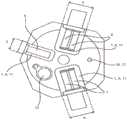
图1示意性地示出了根据本发明的没有转盘的优选的装置的平面图。该装置具有三个磁控溅射装置2,3,4,其中一个设计在单磁控布置2中,两个设计在双磁控布置3,4中。磁控溅射装置2包括磁控电极5,溅射气体11和可选地,反应气体8,并且处于真空1中。磁控溅射装置3,4分别包括两个磁控电极6,7,溅射气体11,以及可选地,反应气体9,并且处于真空1中。等离子体源12和光度计16和/或椭圆偏振法兰17位于磁控溅射装置2、3、4的附近。Figure 1 schematically shows a plan view of a preferred device according to the invention without a turntable. The device has three
图2示意性地示出了转盘的优选实施例的平面图。转盘10位于装置中,并且在该示例中拥有十个相同的基板支架9。Figure 2 schematically shows a plan view of a preferred embodiment of the turntable. A
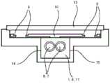
图3示意性地示出了具有转盘10的装置的优选实施例的侧视图。磁控溅射装置的横截面是可见的,它包括两个圆柱形的源材料6,7(双磁控布置)。磁控溅射装置是以气密方式从装置的其余部分在边界壁14、15的侧面处以及在顶部通过转盘10描绘出来的。它包括溅射气体11,可选地,反应气体8,并且处于真空1中。转盘10的两个基板支架9示出或在横截面中可见。盖13位于转盘10的上方且有边界壁,该边界壁位于转盘10的侧面,以气密方式封闭装置。FIG. 3 schematically shows a side view of a preferred embodiment of the device with a
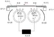
图4示出了根据现有技术的溅射装置,其具有对称极性的圆柱形双磁控布置。Figure 4 shows a sputtering device according to the prior art with a cylindrical dual magnetron arrangement of symmetrical polarity.
发生器为电源提供双极性脉冲电压,脉冲具有正弦、矩形或其他脉冲模式。The generator provides a bipolar pulse voltage to the power supply, the pulses have a sinusoidal, rectangular or other pulse pattern.
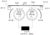
图5示出了根据本发明的溅射装置,其具有不对成极性的圆柱形双磁控管。在该示例中,发生器向电源提供双极性脉冲电压,具有正弦脉冲。这里的校正孔大部分从涂层区域去除。Figure 5 shows a sputtering device according to the invention with asymmetrically polarized cylindrical double magnetrons. In this example, the generator supplies a bipolar pulsed voltage to the power supply, with sinusoidal pulses. Here the correction holes are mostly removed from the coated area.
通过质点网格法Particle-in-Cell等离子体模拟方法检查了图5示出的圆柱形双磁控布置。The cylindrical dual magnetron arrangement shown in Fig. 5 was examined by the Particle-in-Cell plasma simulation method.
模拟参数的编译如下:The simulation parameters are compiled as follows:
型号尺寸:800 x 600 x 400mm2Model size: 800 x 600 x 400mm2
网格数量:100 x 150 x 100Number of grids: 100 x 150 x 100
时间步长:5e-11sTime step: 5e-11 s
时间间隔:250µsTime Interval: 250µs
长度,气缸靶:513mmLength, cylinder target: 513mm
靶直径:138 mmTarget diameter: 138mm
激励频率:40 kHzExcitation frequency: 40 kHz
模型功率:1W(时间平均值)Model power: 1W (time average)
最高电压差:1000VMaximum voltage difference: 1000V
二次电子产额:12%Secondary electronics output: 12%
靶电子捕获:100%Target electron capture: 100%
剩磁:1.4TRemanence: 1.4T
磁化率:1.05Magnetic susceptibility: 1.05
磁轭敏感度:1000Yoke Sensitivity: 1000
磁倾角:向内±6°Magnetic inclination: inward ±6°
进入到两个圆柱形靶中的电馈送以双极性方式进行。在这一方面,靶间的电压差是预先定义的。在模拟过程中,会根据接收到的正电荷和负电荷自动得出与质量(=腔室壁)的电位差。靶以正弦信号的形式周期性地反转极性。激励频率为40 kHz。The electrical feed into the two cylindrical targets is bipolar. In this aspect, the voltage difference between the targets is predefined. During the simulation, the potential difference to the mass (=chamber wall) is automatically derived from the received positive and negative charges. The target reverses polarity periodically in the form of a sinusoidal signal. The excitation frequency is 40 kHz.
首先为磁体假设一套用于圆柱形靶的商业磁体模型。在模型中,两组磁体都向中心倾斜10°。在标准设计中,两组磁体具有相同的极性,即,外磁环的上侧至北极,内磁体的上侧至南极。该配置将在下面被称为“偶数”。在根据本发明的情况下,第二组磁体(在图5的右手侧)的极性相反。在下文中,该配置将在下面被称为“奇数”。A set of commercial magnet models for cylindrical targets is first assumed for the magnets. In the model, both sets of magnets are tilted 10° towards the center. In the standard design, the two sets of magnets have the same polarity, ie, the upper side of the outer magnetic ring to the north pole, and the upper side of the inner magnet to the south pole. This configuration will be referred to as "even" below. In the case according to the invention, the polarity of the second set of magnets (on the right hand side in FIG. 5 ) is reversed. Hereinafter, this configuration will be referred to as "odd number" below.
在模拟过程中,持续检测耗散的等离子体功率(参考时间步长前后带电粒子的动能),并分别累积超过0.1µs。靶间的电压差由比例调节器通过比较期望功率和实际功率的方法来调节。图6可以看到由此产生的电压和功率随时间变化的曲线。在假定准静态放电状态之前,通常需要50µs以上的时间。此外,明显的是,在根据本发明的“奇数”配置中,采用较小的电压差来平衡,即以低阻抗放电。因此,在最后12个半波中,即在102.5µs到250µs的时间间隔内,以2.5µs的步长平均用于测定溅射侵蚀分布的靶上的离子流轮廓。图7示出了离子流的三维视图。在靶处离子流所累积的离子流密度对于“偶数”配置(见图8)显示对角对称分布,对于“奇数”配置(见图9)显示单边分布。During the simulation, the dissipated plasma power (kinetic energy of charged particles before and after the reference time step) was continuously detected and accumulated over 0.1 µs respectively. The voltage difference between the targets is regulated by a proportional regulator by comparing the desired power with the actual power. Figure 6 shows the resulting voltage and power versus time curves. It typically takes more than 50µs before assuming a quasi-static discharge state. Furthermore, it is evident that in the "odd" configuration according to the invention, a smaller voltage difference is used to balance, ie to discharge with low impedance. Therefore, the ion current profile on the target used to determine the sputter erosion profile was averaged in steps of 2.5 µs during the last 12 half-waves, ie in the time interval from 102.5 µs to 250 µs. Figure 7 shows a three-dimensional view of ion flow. The ion current density accumulated by the ion current at the target shows a diagonally symmetric distribution for the "even" configuration (see Figure 8) and a unilateral distribution for the "odd" configuration (see Figure 9).
此外,可以看出,在“奇数”配置中,流密度的绝对值更高,这与已经提到的更低的等离子体阻抗有关。只要用于溅射效果的电压足够大,更低的等离子体阻抗就是有利的,因为通常减少了不希望有的放电(电弧)的倾向。图9中更高的离子流密度也是有利的,因为它能带来更高的速率。Furthermore, it can be seen that the absolute value of the flux density is higher in the 'odd' configuration, which correlates with the already mentioned lower plasma impedance. As long as the voltage used for the sputtering effect is large enough, a lower plasma impedance is advantageous, as the tendency to undesired electrical discharges (arcing) is generally reduced. A higher ion current density in Figure 9 is also beneficial because it leads to higher velocities.
图10示出了第二布置中在靶处累积的离子流密度。在这一方面,粒子流密度的梯度相反,从而导致小的向外的去除率。使用另外的分布掩模,因而可以产生更大的层厚度梯度。Figure 10 shows the ion current density accumulated at the target in the second arrangement. In this respect, the gradient of the particle flux density is reversed, resulting in a small outward removal rate. Using an additional profile mask, larger layer thickness gradients can thus be produced.
由于靶在涂层过程中旋转,且基板在两个靶上的转盘上旋转,因此,靶区离子流轮廓的平均值对靶区域的侵蚀轮廓和层厚度分布都有决定性的影响。当靶上的Ar离子能量分布近似恒定时,离子流轮廓与溅射速率成正比。如图11所示,时间平均间隔为100-25µs,即超过正弦激励的12个半周期。Since the target rotates during the coating process and the substrate rotates on the turntables on both targets, the mean value of the ion current profile in the target area has a decisive influence on the erosion profile and the layer thickness distribution in the target area. When the energy distribution of Ar ions on the target is approximately constant, the ion flow profile is proportional to the sputtering rate. As shown in Figure 11, the temporal averaging interval is 100-25 µs, i.e. over 12 half periods of the sinusoidal excitation.
对于“偶数”布置,可以认识到入射涂覆速率导致了基板区域。该区域包括270至47mm(基板直径200mm)的径向位置。使用掩模时,向内的速率必须设置为最小值70(相对速率)。For the "even" arrangement, it can be realized that the incident coating rate results in substrate area. This area includes radial positions from 270 to 47mm (substrate diameter 200mm). When using a mask, the inward velocity must be set to a minimum of 70 (relative velocity).
相比之下,在“奇数”布置中,即使没有均匀性掩模,基板上也会产生近似平滑、均匀的层厚度轮廓。在磁体极性正确布置的情况下,层厚度的减少因而可以通过在转盘半径上的“奇数”配置来近似补偿。在相同的溅射功率下,涂层只有小部分流向被筛选的基板,从而获得更高的涂覆速率。In contrast, in the "odd" arrangement, an approximately smooth, uniform layer thickness profile is produced on the substrate even without a uniformity mask. With the correct arrangement of magnet polarity, the reduction in layer thickness can thus be approximately compensated by an "odd" configuration on the turntable radius. Under the same sputtering power, only a small part of the coating flows to the substrate being screened, resulting in a higher coating rate.
Claims (28)
Applications Claiming Priority (3)
| Application Number | Priority Date | Filing Date | Title |
|---|---|---|---|
| DE102018213534.7 | 2018-08-10 | ||
| DE102018213534.7ADE102018213534A1 (en) | 2018-08-10 | 2018-08-10 | Device and method for producing layers with improved uniformity in coating systems with horizontally rotating substrate guidance |
| PCT/EP2019/071460WO2020030794A1 (en) | 2018-08-10 | 2019-08-09 | Device and method for producing layers with improved uniformity in coating systems with horizontally rotating substrate guiding |
Publications (2)
| Publication Number | Publication Date |
|---|---|
| CN112585293A CN112585293A (en) | 2021-03-30 |
| CN112585293Btrue CN112585293B (en) | 2023-06-23 |
Family
ID=67659849
Family Applications (1)
| Application Number | Title | Priority Date | Filing Date |
|---|---|---|---|
| CN201980052966.0AActiveCN112585293B (en) | 2018-08-10 | 2019-08-09 | Device and method for producing layers in a coating system |
Country Status (6)
| Country | Link |
|---|---|
| US (1) | US12428720B2 (en) |
| EP (1) | EP3833799A1 (en) |
| JP (1) | JP7277565B2 (en) |
| CN (1) | CN112585293B (en) |
| DE (1) | DE102018213534A1 (en) |
| WO (1) | WO2020030794A1 (en) |
Families Citing this family (5)
| Publication number | Priority date | Publication date | Assignee | Title |
|---|---|---|---|---|
| EP3722451A1 (en) | 2019-04-09 | 2020-10-14 | FRAUNHOFER-GESELLSCHAFT zur Förderung der angewandten Forschung e.V. | Device and method for coating substrates with planar or shaped surfaces by magnetron sputtering |
| DE102020201829A1 (en) | 2020-02-13 | 2021-08-19 | Fraunhofer-Gesellschaft zur Förderung der angewandten Forschung eingetragener Verein | Device and method for producing layers with improved uniformity in coating systems with horizontally rotating substrate guides with additional plasma sources |
| DE102020117347A1 (en) | 2020-07-01 | 2022-01-05 | VON ARDENNE Asset GmbH & Co. KG | Magnetron arrangement |
| DE102021100126A1 (en) | 2021-01-07 | 2022-07-07 | VON ARDENNE Asset GmbH & Co. KG | Coating arrangement and method |
| EP4270444A1 (en)* | 2022-04-27 | 2023-11-01 | Bühler Alzenau GmbH | Magnetron sputtering system with tubular sputter cathode and method for controlling a layer thickness |
Citations (3)
| Publication number | Priority date | Publication date | Assignee | Title |
|---|---|---|---|---|
| JPH0874051A (en)* | 1994-09-01 | 1996-03-19 | Fujitsu Ltd | Magnetron sputtering equipment |
| US6488824B1 (en)* | 1998-11-06 | 2002-12-03 | Raycom Technologies, Inc. | Sputtering apparatus and process for high rate coatings |
| DE102011085888A1 (en)* | 2011-11-08 | 2013-05-08 | Von Ardenne Anlagentechnik Gmbh | Coating a substrate with a mixing layer or an alloy layer by magnetron sputtering, by depositing two tube magnetrons that are arranged next to each other in a coating chamber, whose outer surfaces comprise a sputterable target material |
Family Cites Families (32)
| Publication number | Priority date | Publication date | Assignee | Title |
|---|---|---|---|---|
| US4851095A (en) | 1988-02-08 | 1989-07-25 | Optical Coating Laboratory, Inc. | Magnetron sputtering apparatus and process |
| US5096562A (en)* | 1989-11-08 | 1992-03-17 | The Boc Group, Inc. | Rotating cylindrical magnetron structure for large area coating |
| DE4038497C1 (en)* | 1990-12-03 | 1992-02-20 | Leybold Ag, 6450 Hanau, De | |
| JPH04358064A (en)* | 1991-01-23 | 1992-12-11 | Ulvac Japan Ltd | Magnetron sputtering cathode |
| US5415754A (en) | 1993-10-22 | 1995-05-16 | Sierra Applied Sciences, Inc. | Method and apparatus for sputtering magnetic target materials |
| US5609772A (en) | 1995-06-05 | 1997-03-11 | International Business Machines Corporation | Cube maskless lead open process using chemical mechanical polish/lead-tip expose process |
| US6726993B2 (en)* | 1997-12-02 | 2004-04-27 | Teer Coatings Limited | Carbon coatings, method and apparatus for applying them, and articles bearing such coatings |
| DE19827587A1 (en)* | 1998-06-20 | 1999-12-23 | Ardenne Anlagentech Gmbh | Double-magnetron sputtering unit for large area reactive plasma-enhanced deposition of e.g. light absorbing layers on metal strips for solar absorbers or heat reflective layers on window glass |
| JP5493196B2 (en) | 2000-02-23 | 2014-05-14 | エリコン・アドバンスト・テクノロジーズ・アクチェンゲゼルシャフト | Method for controlling plasma density or its distribution |
| DE10141696A1 (en)* | 2001-08-25 | 2003-03-13 | Bosch Gmbh Robert | Process for producing a nanostructured functional coating and coating that can be produced with it |
| CN1745453B (en)* | 2002-11-29 | 2011-08-31 | Oc欧瑞康巴尔斯公司 | Method and apparatus for plasma treatment of surface in vacuum |
| DE10347521A1 (en) | 2002-12-04 | 2004-06-24 | Leybold Optics Gmbh | Method for producing a multilayer layer and device for carrying out the method |
| US7101466B2 (en) | 2003-09-19 | 2006-09-05 | Kdf Electronic + Vacuum Services Inc | Linear sweeping magnetron sputtering cathode and scanning in-line system for arc-free reactive deposition and high target utilization |
| SE0303136D0 (en)* | 2003-11-24 | 2003-11-24 | Chemfilt R & D Ab | Method and apparatus for reactive soil-gas-plasma deposition |
| US9349576B2 (en) | 2006-03-17 | 2016-05-24 | Angstrom Sciences, Inc. | Magnetron for cylindrical targets |
| EP1840936A1 (en) | 2006-03-29 | 2007-10-03 | Applied Materials GmbH & Co. KG | Sputtering chamber for coating a substrate |
| JP5283084B2 (en)* | 2007-04-06 | 2013-09-04 | 国立大学法人東北大学 | Magnetron sputtering equipment |
| JP2009024230A (en) | 2007-07-20 | 2009-02-05 | Kobe Steel Ltd | Sputtering apparatus |
| GB0715879D0 (en) | 2007-08-15 | 2007-09-26 | Gencoa Ltd | Low impedance plasma |
| US8246794B2 (en) | 2007-12-07 | 2012-08-21 | Oc Oerlikon Blazers Ag | Method of magnetron sputtering and a method for determining a power modulation compensation function for a power supply applied to a magnetron sputtering source |
| US20120138452A1 (en)* | 2009-04-17 | 2012-06-07 | The Regents Of The University Of California | Method and Apparatus for Super-High Rate Deposition |
| DE102010000853A1 (en) | 2010-01-13 | 2011-07-14 | Federal-Mogul Wiesbaden GmbH, 65201 | Holder for galvanic coating of plain bearings and tools with a holder |
| JP5619666B2 (en) | 2010-04-16 | 2014-11-05 | ジェイディーエス ユニフェイズ コーポレーションJDS Uniphase Corporation | Ring cathode for use in magnetron sputtering devices |
| EP2549521A1 (en)* | 2011-07-21 | 2013-01-23 | Fraunhofer-Gesellschaft zur Förderung der angewandten Forschung e.V. | Method and device for producing low-particle layers on substrates |
| DE102013207771A1 (en) | 2013-04-29 | 2014-10-30 | Robert Bosch Gmbh | Pump, in particular fuel pump |
| DE102013208771B4 (en)* | 2013-05-13 | 2019-11-21 | Fraunhofer-Gesellschaft zur Förderung der angewandten Forschung e.V. | Method for influencing the layer thickness distribution on substrates and use of a device for carrying out the method |
| EP2811509A1 (en)* | 2013-06-07 | 2014-12-10 | Soleras Advanced Coatings bvba | Electronic configuration for magnetron sputter deposition systems |
| PL2811508T3 (en)* | 2013-06-07 | 2019-10-31 | Soleras Advanced Coatings Bvba | Gas configuration for magnetron deposition systems |
| DE102013221029A1 (en) | 2013-10-16 | 2015-04-16 | Fraunhofer-Gesellschaft zur Förderung der angewandten Forschung e.V. | Method and device for producing uniform layers on moving substrates and layers produced in this way |
| EP2963145B1 (en)* | 2014-06-30 | 2018-01-31 | IHI Hauzer Techno Coating B.V. | Coating and method for its deposition to operate in boundary lubrication conditions and at elevated temperatures |
| DE102015200488A1 (en) | 2015-01-14 | 2016-07-14 | Fraunhofer-Gesellschaft zur Förderung der angewandten Forschung e.V. | Electrically controllable interference color filter and its use |
| KR102636365B1 (en)* | 2016-05-25 | 2024-02-15 | 삼성디스플레이 주식회사 | Sputtering apparauts and sputtering method using the same |
- 2018
- 2018-08-10DEDE102018213534.7Apatent/DE102018213534A1/enactivePending
- 2019
- 2019-08-09EPEP19753322.7Apatent/EP3833799A1/enactivePending
- 2019-08-09USUS17/267,106patent/US12428720B2/enactiveActive
- 2019-08-09CNCN201980052966.0Apatent/CN112585293B/enactiveActive
- 2019-08-09WOPCT/EP2019/071460patent/WO2020030794A1/ennot_activeCeased
- 2019-08-09JPJP2021507037Apatent/JP7277565B2/enactiveActive
Patent Citations (3)
| Publication number | Priority date | Publication date | Assignee | Title |
|---|---|---|---|---|
| JPH0874051A (en)* | 1994-09-01 | 1996-03-19 | Fujitsu Ltd | Magnetron sputtering equipment |
| US6488824B1 (en)* | 1998-11-06 | 2002-12-03 | Raycom Technologies, Inc. | Sputtering apparatus and process for high rate coatings |
| DE102011085888A1 (en)* | 2011-11-08 | 2013-05-08 | Von Ardenne Anlagentechnik Gmbh | Coating a substrate with a mixing layer or an alloy layer by magnetron sputtering, by depositing two tube magnetrons that are arranged next to each other in a coating chamber, whose outer surfaces comprise a sputterable target material |
Also Published As
| Publication number | Publication date |
|---|---|
| JP7277565B2 (en) | 2023-05-19 |
| JP2021534323A (en) | 2021-12-09 |
| US12428720B2 (en) | 2025-09-30 |
| US20210164092A1 (en) | 2021-06-03 |
| DE102018213534A1 (en) | 2020-02-13 |
| CN112585293A (en) | 2021-03-30 |
| EP3833799A1 (en) | 2021-06-16 |
| WO2020030794A1 (en) | 2020-02-13 |
Similar Documents
| Publication | Publication Date | Title |
|---|---|---|
| CN112585293B (en) | Device and method for producing layers in a coating system | |
| JP5048229B2 (en) | Magnetron sputtering device | |
| US6916407B2 (en) | Target comprising thickness profiling for an RF magnetron | |
| CN101792895B (en) | Cathodic vacuum arc source film depositing device and method for depositing film | |
| JP6707559B2 (en) | Method of manufacturing coated substrate | |
| TWI539023B (en) | Reactive sputtering with multiple sputtering sources | |
| DK2735018T3 (en) | PROCEDURE AND APPARATUS FOR PREPARING LOW PARTICLES | |
| US6419800B2 (en) | Film-forming apparatus and film-forming method | |
| CN120591743A (en) | Method and apparatus for controlling stress changes in a material layer formed by pulsed DC PVD | |
| US20060188660A1 (en) | Method for depositing multilayer coatings | |
| TWI464285B (en) | Film formation equipment and film formation method | |
| CN201660693U (en) | Cathodic vacuum arc source film deposition device | |
| CN115103928A (en) | Device and method for producing layers with improved uniformity in coating systems with horizontally rotating substrate-guided and further plasma sources | |
| JP2011124215A (en) | Ion beam generator, and cleaning method thereof | |
| WO2012066080A1 (en) | Sputtering apparatus and method | |
| US20100264022A1 (en) | Sputtering And Ion Beam Deposition | |
| JP5783613B2 (en) | Magnetron coating module and magnetron coating method | |
| US11094515B2 (en) | Sputtering apparatus and sputtering method | |
| JP2009275281A (en) | Sputtering method and system | |
| US6423191B1 (en) | Sputtering method and apparatus for depositing a coating onto substrate | |
| JP5312138B2 (en) | Sputtering method | |
| KR20170095463A (en) | Hybrid physical-vapor epitaxy method and apparatus for fabrication of thin films | |
| CN115404437A (en) | Sputtering method and sputtering apparatus | |
| JP2010285647A (en) | Film deposition apparatus and film deposition method | |
| JP2003013217A (en) | Method and apparatus for forming dielectric film |
Legal Events
| Date | Code | Title | Description |
|---|---|---|---|
| PB01 | Publication | ||
| PB01 | Publication | ||
| SE01 | Entry into force of request for substantive examination | ||
| SE01 | Entry into force of request for substantive examination | ||
| GR01 | Patent grant | ||
| GR01 | Patent grant |