CN112582476B - Semiconductor device and method of forming the same - Google Patents
Semiconductor device and method of forming the sameDownload PDFInfo
- Publication number
- CN112582476B CN112582476BCN202011432877.XACN202011432877ACN112582476BCN 112582476 BCN112582476 BCN 112582476BCN 202011432877 ACN202011432877 ACN 202011432877ACN 112582476 BCN112582476 BCN 112582476B
- Authority
- CN
- China
- Prior art keywords
- dielectric layer
- gate structure
- forming
- sides
- source
- Prior art date
- Legal status (The legal status is an assumption and is not a legal conclusion. Google has not performed a legal analysis and makes no representation as to the accuracy of the status listed.)
- Active
Links
- 239000004065semiconductorSubstances0.000titleclaimsabstractdescription65
- 238000000034methodMethods0.000titleclaimsabstractdescription59
- 239000000758substrateSubstances0.000claimsabstractdescription29
- 239000000463materialSubstances0.000claimsdescription37
- VYPSYNLAJGMNEJ-UHFFFAOYSA-NSilicium dioxideChemical compoundO=[Si]=OVYPSYNLAJGMNEJ-UHFFFAOYSA-N0.000claimsdescription10
- 229910052814silicon oxideInorganic materials0.000claimsdescription10
- 229910052581Si3N4Inorganic materials0.000claimsdescription9
- 238000005530etchingMethods0.000claimsdescription9
- HQVNEWCFYHHQES-UHFFFAOYSA-Nsilicon nitrideChemical compoundN12[Si]34N5[Si]62N3[Si]51N64HQVNEWCFYHHQES-UHFFFAOYSA-N0.000claimsdescription9
- 238000004519manufacturing processMethods0.000abstractdescription25
- 125000006850spacer groupChemical group0.000description14
- 238000010586diagramMethods0.000description4
- 230000003071parasitic effectEffects0.000description4
- 230000000717retained effectEffects0.000description4
- 230000009286beneficial effectEffects0.000description3
- 230000015572biosynthetic processEffects0.000description3
- 230000010354integrationEffects0.000description3
- 229910052751metalInorganic materials0.000description3
- 239000002184metalSubstances0.000description3
- 238000000407epitaxyMethods0.000description2
- 239000012212insulatorSubstances0.000description2
- 229910021420polycrystalline siliconInorganic materials0.000description2
- 229920005591polysiliconPolymers0.000description2
- 229910010271silicon carbideInorganic materials0.000description2
- JBRZTFJDHDCESZ-UHFFFAOYSA-NAsGaChemical compound[As]#[Ga]JBRZTFJDHDCESZ-UHFFFAOYSA-N0.000description1
- GYHNNYVSQQEPJS-UHFFFAOYSA-NGalliumChemical compound[Ga]GYHNNYVSQQEPJS-UHFFFAOYSA-N0.000description1
- 229910001218Gallium arsenideInorganic materials0.000description1
- 229910004298SiO 2Inorganic materials0.000description1
- XUIMIQQOPSSXEZ-UHFFFAOYSA-NSiliconChemical compound[Si]XUIMIQQOPSSXEZ-UHFFFAOYSA-N0.000description1
- 229910000577Silicon-germaniumInorganic materials0.000description1
- LEVVHYCKPQWKOP-UHFFFAOYSA-N[Si].[Ge]Chemical compound[Si].[Ge]LEVVHYCKPQWKOP-UHFFFAOYSA-N0.000description1
- 238000004140cleaningMethods0.000description1
- 230000000694effectsEffects0.000description1
- 229910052733galliumInorganic materials0.000description1
- 229910052732germaniumInorganic materials0.000description1
- GNPVGFCGXDBREM-UHFFFAOYSA-Ngermanium atomChemical compound[Ge]GNPVGFCGXDBREM-UHFFFAOYSA-N0.000description1
- 229910052738indiumInorganic materials0.000description1
- APFVFJFRJDLVQX-UHFFFAOYSA-Nindium atomChemical compound[In]APFVFJFRJDLVQX-UHFFFAOYSA-N0.000description1
- 238000012986modificationMethods0.000description1
- 230000004048modificationEffects0.000description1
- 238000005457optimizationMethods0.000description1
- 229910052710siliconInorganic materials0.000description1
- 239000010703siliconSubstances0.000description1
- HBMJWWWQQXIZIP-UHFFFAOYSA-Nsilicon carbideChemical compound[Si+]#[C-]HBMJWWWQQXIZIP-UHFFFAOYSA-N0.000description1
- -1silicon carbide nitrideChemical class0.000description1
- 238000004381surface treatmentMethods0.000description1
Images


Classifications
- H—ELECTRICITY
- H10—SEMICONDUCTOR DEVICES; ELECTRIC SOLID-STATE DEVICES NOT OTHERWISE PROVIDED FOR
- H10D—INORGANIC ELECTRIC SEMICONDUCTOR DEVICES
- H10D30/00—Field-effect transistors [FET]
- H10D30/60—Insulated-gate field-effect transistors [IGFET]
- H—ELECTRICITY
- H10—SEMICONDUCTOR DEVICES; ELECTRIC SOLID-STATE DEVICES NOT OTHERWISE PROVIDED FOR
- H10D—INORGANIC ELECTRIC SEMICONDUCTOR DEVICES
- H10D30/00—Field-effect transistors [FET]
- H10D30/01—Manufacture or treatment
- H10D30/021—Manufacture or treatment of FETs having insulated gates [IGFET]
- H—ELECTRICITY
- H10—SEMICONDUCTOR DEVICES; ELECTRIC SOLID-STATE DEVICES NOT OTHERWISE PROVIDED FOR
- H10D—INORGANIC ELECTRIC SEMICONDUCTOR DEVICES
- H10D30/00—Field-effect transistors [FET]
- H10D30/60—Insulated-gate field-effect transistors [IGFET]
- H10D30/601—Insulated-gate field-effect transistors [IGFET] having lightly-doped drain or source extensions, e.g. LDD IGFETs or DDD IGFETs
- H10D30/608—Insulated-gate field-effect transistors [IGFET] having lightly-doped drain or source extensions, e.g. LDD IGFETs or DDD IGFETs having non-planar bodies, e.g. having recessed gate electrodes
- H—ELECTRICITY
- H10—SEMICONDUCTOR DEVICES; ELECTRIC SOLID-STATE DEVICES NOT OTHERWISE PROVIDED FOR
- H10D—INORGANIC ELECTRIC SEMICONDUCTOR DEVICES
- H10D62/00—Semiconductor bodies, or regions thereof, of devices having potential barriers
- H10D62/10—Shapes, relative sizes or dispositions of the regions of the semiconductor bodies; Shapes of the semiconductor bodies
- H10D62/124—Shapes, relative sizes or dispositions of the regions of semiconductor bodies or of junctions between the regions
- H—ELECTRICITY
- H10—SEMICONDUCTOR DEVICES; ELECTRIC SOLID-STATE DEVICES NOT OTHERWISE PROVIDED FOR
- H10D—INORGANIC ELECTRIC SEMICONDUCTOR DEVICES
- H10D64/00—Electrodes of devices having potential barriers
- H10D64/20—Electrodes characterised by their shapes, relative sizes or dispositions
- H10D64/23—Electrodes carrying the current to be rectified, amplified, oscillated or switched, e.g. sources, drains, anodes or cathodes
- H10D64/251—Source or drain electrodes for field-effect devices
- H10D64/257—Source or drain electrodes for field-effect devices for lateral devices wherein the source or drain electrodes are characterised by top-view geometrical layouts, e.g. interdigitated, semi-circular, annular or L-shaped electrodes
Landscapes
- Insulated Gate Type Field-Effect Transistor (AREA)
Abstract
Description
Translated fromChinese技术领域technical field
本发明涉及半导体制造技术领域,尤其涉及一种半导体器件及其形成方法。The present invention relates to the technical field of semiconductor manufacturing, and in particular, to a semiconductor device and a method for forming the same.
背景技术Background technique
随着半导体技术的不断发展,集成电路性能的提高主要是通过不断缩小集成电路器件的尺寸,以提高它的速度来实现的。目前,由于在追求高器件密度、高性能和低成本中半导体工业已经进步到纳米技术工艺节点,特别是当半导体器件尺寸降到纳米级别时,半导体器件的制备受到各种物理极限的限制。具体而言,当半导体器件的尺寸降到纳米级别时,器件中栅极的沟道尺寸也相应缩小,半导体器件的短沟道效应也越来越严重。With the continuous development of semiconductor technology, the improvement of integrated circuit performance is mainly achieved by continuously reducing the size of integrated circuit devices to increase its speed. Currently, as the semiconductor industry has progressed to nanotechnology process nodes in pursuit of high device density, high performance, and low cost, especially when the size of semiconductor devices is reduced to the nanometer scale, the fabrication of semiconductor devices is limited by various physical limits. Specifically, when the size of a semiconductor device is reduced to the nanometer level, the channel size of the gate in the device is correspondingly reduced, and the short-channel effect of the semiconductor device is becoming more and more serious.
在现有的一种半导体器件的形成工艺中,采用外延生长的方式,在栅极结构的两侧形成源漏外延区(Epitaxy,又称为EPI),以实现传统工艺中的源漏掺杂区的功能。其中,在栅极结构的顶部两侧的源漏外延区的宽度小于栅极结构底部两侧的源漏外延区的宽度(如台阶形状),能够有效控制寄生电容的产生。In an existing process for forming a semiconductor device, a source-drain epitaxial region (Epitaxy, also known as EPI) is formed on both sides of the gate structure by means of epitaxial growth, so as to realize the source-drain doping in the traditional process. area function. Wherein, the width of the source-drain epitaxial regions on both sides of the top of the gate structure is smaller than the width of the source-drain epitaxial regions on both sides of the bottom of the gate structure (eg step shape), which can effectively control the generation of parasitic capacitance.
然而,在现有的形成源漏外延区的技术中,工艺整合复杂度和生产成本均较高。However, in the existing technology for forming the source-drain epitaxial region, the process integration complexity and the production cost are relatively high.
发明内容SUMMARY OF THE INVENTION
本发明解决的技术问题是提供一种半导体器件及其形成方法,可以有效降低工艺复杂度和生产成本,提高生产稳定性和器件性能。The technical problem solved by the present invention is to provide a semiconductor device and a method for forming the same, which can effectively reduce process complexity and production cost, and improve production stability and device performance.
为解决上述技术问题,本发明实施例提供一种半导体器件的形成方法,包括:提供半导体衬底;在所述半导体衬底的表面形成栅极结构;形成第一介质层,所述第一介质层位于所述栅极结构的两侧,且所述第一介质层的顶部表面低于所述栅极结构的顶部表面;形成第二介质层,所述第二介质层位于所述第一介质层的表面以及位于所述栅极结构的两侧,且所述第二介质层的宽度小于所述第一介质层的宽度;去除所第一介质层,以暴露出所述第二介质层下方的栅极结构的侧壁表面;形成源漏外延区,所述源漏外延区位于所述第二介质层的两侧以及所述第二介质层下方的栅极结构的两侧。In order to solve the above technical problems, an embodiment of the present invention provides a method for forming a semiconductor device, including: providing a semiconductor substrate; forming a gate structure on the surface of the semiconductor substrate; forming a first dielectric layer, the first dielectric layers are located on both sides of the gate structure, and the top surface of the first dielectric layer is lower than the top surface of the gate structure; a second dielectric layer is formed, and the second dielectric layer is located on the first dielectric the surface of the layer and on both sides of the gate structure, and the width of the second dielectric layer is smaller than the width of the first dielectric layer; removing the first dielectric layer to expose the bottom of the second dielectric layer The sidewall surface of the gate structure is formed; the source-drain epitaxial region is formed, and the source-drain epitaxial region is located on both sides of the second dielectric layer and on both sides of the gate structure under the second dielectric layer.
可选的,形成第一介质层包括:形成初始第一介质层,所述初始第一介质层覆盖所述栅极结构;对所述初始第一介质层进行平坦化;对所述初始第一介质层进行刻蚀,以形成第一介质层。Optionally, forming the first dielectric layer includes: forming an initial first dielectric layer, the initial first dielectric layer covering the gate structure; planarizing the initial first dielectric layer; The dielectric layer is etched to form a first dielectric layer.
可选的,所述第一介质层与所述第二介质层的刻蚀比大于预设阈值。Optionally, an etching ratio of the first dielectric layer to the second dielectric layer is greater than a preset threshold.
可选的,所述第一介质层的材料选自:SiCN、氧化硅以及氮化硅;和/或,所述第二介质层的材料选自:氧化硅以及氮化硅;其中,所述第一介质层的材料不同于所述第二介质层的材料。Optionally, the material of the first dielectric layer is selected from: SiCN, silicon oxide and silicon nitride; and/or, the material of the second dielectric layer is selected from: silicon oxide and silicon nitride; wherein, the The material of the first dielectric layer is different from the material of the second dielectric layer.
可选的,形成第二介质层包括:形成初始第二介质层,所述初始第二介质层覆盖所述栅极结构以及所述第一介质层;对所述初始第二介质层进行刻蚀,以形成第二介质层。Optionally, forming the second dielectric layer includes: forming an initial second dielectric layer, the initial second dielectric layer covering the gate structure and the first dielectric layer; and etching the initial second dielectric layer , to form the second dielectric layer.
可选的,所述第二介质层的顶部表面与所述栅极结构的顶部表面齐平。Optionally, the top surface of the second dielectric layer is flush with the top surface of the gate structure.
可选的,所述源漏外延区的顶部表面低于所述栅极结构的顶部表面。Optionally, the top surface of the source-drain epitaxial region is lower than the top surface of the gate structure.
可选的,在所述半导体衬底的表面形成栅极结构包括:形成侧墙,所述侧墙位于所述栅极结构的两侧;其中,所述第一介质层以及所述第二介质层位于所述侧墙的两侧。Optionally, forming the gate structure on the surface of the semiconductor substrate includes: forming spacers, the spacers are located on both sides of the gate structure; wherein, the first dielectric layer and the second dielectric Layers are located on both sides of the side walls.
为解决上述技术问题,本发明实施例提供一种半导体器件,包括:半导体衬底;栅极结构,位于所述半导体衬底的表面;第二介质层,位于所述栅极结构的两侧;源漏外延区,位于所述第二介质层的两侧以及所述第二介质层下方的栅极结构的两侧;其中,所述源漏外延区是在去除第一介质层,以暴露出所述第二介质层下方的栅极结构的侧壁表面之后形成的;所述第一介质层是在形成第二介质层之前形成的,所述第一介质层位于所述栅极结构的两侧,且所述第一介质层的顶部表面低于所述栅极结构的顶部表面;所述第二介质层位于所述第一介质层的表面且所述第二介质层的宽度小于所述第一介质层的宽度。In order to solve the above technical problem, an embodiment of the present invention provides a semiconductor device, including: a semiconductor substrate; a gate structure, located on the surface of the semiconductor substrate; a second dielectric layer, located on both sides of the gate structure; source-drain epitaxial regions, located on both sides of the second dielectric layer and on both sides of the gate structure under the second dielectric layer; wherein, the source-drain epitaxial regions are removing the first dielectric layer to expose The second dielectric layer is formed after the sidewall surface of the gate structure; the first dielectric layer is formed before the second dielectric layer is formed, and the first dielectric layer is located on two sides of the gate structure. side, and the top surface of the first dielectric layer is lower than the top surface of the gate structure; the second dielectric layer is located on the surface of the first dielectric layer and the width of the second dielectric layer is smaller than the width of the The width of the first dielectric layer.
可选的,所述第二介质层的顶部表面与所述栅极结构的顶部表面齐平。Optionally, the top surface of the second dielectric layer is flush with the top surface of the gate structure.
可选的,所述源漏外延区的顶部表面低于所述栅极结构的顶部表面。Optionally, the top surface of the source-drain epitaxial region is lower than the top surface of the gate structure.
与现有技术相比,本发明实施例的技术方案具有以下有益效果:Compared with the prior art, the technical solutions of the embodiments of the present invention have the following beneficial effects:
在本发明实施例中,通过先形成第一介质层作为牺牲层,可以在需要形成源漏外延区的区域先形成第一介质层,从而在去除第一介质层后,仅需要单次外延生长工艺即可形成具有台阶形状的源漏外延区,相比于现有技术中,需要两次外延生长工艺才能形成具有台阶形状的源漏外延区,采用本发明实施例的方案,可以有效降低工艺复杂度和生产成本,提高生产稳定性和器件性能。进一步地,本发明实施例中的技术方案,与现有技术中的生产工艺完全兼容,无需引入额外的机台及耗材,无制造污染的风险。In the embodiment of the present invention, by first forming the first dielectric layer as the sacrificial layer, the first dielectric layer can be formed first in the region where the source-drain epitaxial region needs to be formed, so that after the first dielectric layer is removed, only a single epitaxial growth is required A source-drain epitaxial region with a stepped shape can be formed by the process. Compared with the prior art, two epitaxial growth processes are required to form a source-drain epitaxial region with a stepped shape. By using the solution of the embodiment of the present invention, the process can be effectively reduced. Complexity and production cost, improve production stability and device performance. Further, the technical solutions in the embodiments of the present invention are completely compatible with the production processes in the prior art, no additional machines and consumables need to be introduced, and there is no risk of manufacturing pollution.
进一步,在本发明实施例中,通过设置所述第一介质层与所述第二介质层的刻蚀比大于预设阈值,可以在形成第二介质层之后,刻蚀位于所述第二介质层下方的第一介质层时,对需要保留的第二介质层进行有效保护。Further, in the embodiment of the present invention, by setting the etching ratio of the first dielectric layer to the second dielectric layer to be greater than a preset threshold, after the second dielectric layer is formed, the second dielectric layer can be etched on the second dielectric layer. When the first dielectric layer below the layer is used, the second dielectric layer that needs to be retained can be effectively protected.
进一步,所述第一介质层的材料不同于所述第二介质层的材料,有助于在形成第二介质层之后,刻蚀位于所述第二介质层下方的第一介质层时,避免对需要保留的第二介质层产生伤害。Further, the material of the first dielectric layer is different from the material of the second dielectric layer, which helps to prevent the etching of the first dielectric layer under the second dielectric layer after the formation of the second dielectric layer. Damage to the second dielectric layer that needs to be retained.
进一步,所述第二介质层的顶部表面与所述栅极结构的顶部表面齐平,从而可以采用所述栅极结构(包含侧墙)的顶部表面作为平坦化工艺的停止层,有助于降低工艺复杂度。Further, the top surface of the second dielectric layer is flush with the top surface of the gate structure, so that the top surface of the gate structure (including the spacer) can be used as a stop layer for the planarization process, which is helpful for Reduce process complexity.
进一步,所述源漏外延区的顶部表面低于所述栅极结构的顶部表面,从而可以根据具体需求生长适当高度的源漏外延区,降低生产成本。Further, the top surface of the source-drain epitaxial region is lower than the top surface of the gate structure, so that the source-drain epitaxial region can be grown according to specific requirements and the production cost can be reduced.
附图说明Description of drawings
图1至图4是现有技术中一种半导体器件的形成方法中各步骤对应的器件剖面结构示意图;1 to 4 are schematic cross-sectional structural diagrams of the device corresponding to each step in a method for forming a semiconductor device in the prior art;
图5是本发明实施例中一种半导体器件的形成方法的流程图;5 is a flowchart of a method for forming a semiconductor device in an embodiment of the present invention;
图6至图11是本发明实施例中一种半导体器件的形成方法中各步骤对应的器件剖面结构示意图。6 to 11 are schematic cross-sectional structural diagrams of the device corresponding to each step in a method for forming a semiconductor device according to an embodiment of the present invention.
具体实施方式Detailed ways
如前所述,在现有的一种半导体器件的形成工艺中,采用外延生长的方式,在栅极结构的两侧形成源漏外延区,以实现传统工艺中的源漏掺杂区的功能。其中,在栅极结构的顶部两侧的源漏外延区的宽度小于栅极结构底部两侧的源漏外延区的宽度(如台阶形状),能够有效控制寄生电容的产生。然而,在现有的形成源漏外延区的技术中,工艺整合复杂度高,生产成本也高。As mentioned above, in an existing process for forming a semiconductor device, epitaxial growth is used to form source-drain epitaxial regions on both sides of the gate structure, so as to realize the function of the source-drain doped regions in the traditional process . Wherein, the width of the source-drain epitaxial regions on both sides of the top of the gate structure is smaller than the width of the source-drain epitaxial regions on both sides of the bottom of the gate structure (eg step shape), which can effectively control the generation of parasitic capacitance. However, in the existing technology for forming the source-drain epitaxial region, the process integration complexity is high, and the production cost is also high.
图1至图4是现有技术中一种半导体器件的形成方法中各步骤对应的器件剖面结构示意图。1 to 4 are schematic diagrams of cross-sectional structures of a device corresponding to each step in a method for forming a semiconductor device in the prior art.
参照图1,提供半导体衬底100,在所述半导体衬底的表面形成栅极结构110。Referring to FIG. 1, a
其中,所述栅极结构110可以包括栅介质层、栅极材料层和栅硬掩模材料等常规结构,所述栅介质层可以位于所述半导体衬底的表面,所述栅极材料层可以位于所述栅介质层的表面。The
进一步地,所述栅极结构110还可以包括侧墙(Spacer)120,所述侧墙120位于所述栅极结构110的两侧,用于对所述栅极结构110的内部结构进行保护。Further, the
进一步地,所述栅极材料可以采用多晶硅(Poly)材料,还可以采用高K值金属栅(High-K metal gate)材料,以满足多种半导体器件的需要。Further, the gate material may be a polysilicon (Poly) material or a high-K metal gate (High-K metal gate) material to meet the needs of various semiconductor devices.
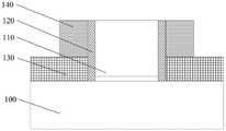
参照图2,形成第一源漏外延区130,所述第一源漏外延区130位于所述栅极结构110的两侧,且所述第一源漏外延区130的顶部表面低于所述栅极结构110的顶部表面。2, a first source-drain
具体地,可以采用外延生长的方式,在栅极结构的底部两侧形成第一源漏外延区,即所述第一源漏外延区130。Specifically, a first source-drain epitaxial region, ie, the first source-drain
需要指出的是,如果在图2中直接生成与栅极结构110的顶部表面齐平的第一源漏外延区130,则容易形成较大的寄生电容,器件性能及稳定性优化受限。It should be pointed out that if the first source-drain
在现有的一种具体应用中,为了控制寄生电容,需要采用较厚的侧墙110,会导致栅极和源极、漏极之间的距离较大,容易产生电性能问题,导致半导体器件性能难以满足需求。In an existing specific application, in order to control the parasitic capacitance, a
参照图3,形成介质层140,所述介质层140位于所述第一源漏外延区130的表面以及位于所述栅极结构110的两侧。Referring to FIG. 3 , a
如图所示,所述介质层140可以位于所述栅极结构110的顶部两侧,具体地,可以位于所述栅极结构110的上半部分的两侧;第一源漏外延区130可以位于所述栅极结构110的底部两侧,具体地,可以位于所述栅极结构110的下半部分的两侧。其中,所述栅极结构110的上半部分与下半部分之间的比例可以根据具体需要进行设置,此处不做限制。As shown in the figure, the
具体地,所述介质层140的宽度小于所述第一源漏外延区130的宽度,从而可以在后续形成第二源漏外延区后,使得第二源漏外延区的宽度小于第一源漏外延区130的宽度,也即实现源漏外延区的台阶形状。Specifically, the width of the
其中,所述宽度的方向平行于所述半导体器件的沟道的方向。Wherein, the direction of the width is parallel to the direction of the channel of the semiconductor device.
参照图4,形成第二源漏外延区150,所述源漏外延区位于所述第一源漏外延区130的表面,且位于所述介质层140的两侧。4 , a second source-drain
在现有技术中,源漏外延区包括第一源漏外延区130与所述第二源漏外延区150,且具有台阶形状。In the prior art, the source-drain epitaxial region includes the first source-drain
本发明的发明人经过研究发现,在现有技术中,至少需要采用两次外延生长工艺才能形成具有台阶形状的源漏外延区。The inventors of the present invention have found through research that in the prior art, at least two epitaxial growth processes are required to form the source-drain epitaxial region with the stepped shape.
具体地,需要先采用第一次外延生长工艺,形成底部台阶区域的源漏外延区,然后形成位于所述栅极结构的顶部两侧的预设区域的介质层,然后采用第一次外延生长工艺,形成顶部台阶区域的源漏外延区。Specifically, it is necessary to use the first epitaxial growth process to form the source-drain epitaxial region in the bottom step region, and then form the dielectric layer in the predetermined region on both sides of the top of the gate structure, and then adopt the first epitaxial growth process to form a source-drain epitaxial region in the top step region.
由于外延生长工艺的工艺耗时较长,工艺复杂度较高,且成品良率较低,容易发生报废现象,导致采用两次外延生长工艺的工艺整合复杂度和生产成本均较高。Since the process time of the epitaxial growth process is long, the process complexity is high, and the yield of the finished product is low, scrapping is prone to occur, resulting in high process integration complexity and production cost of using two epitaxial growth processes.
在本发明实施例中,通过先形成第一介质层作为牺牲层,可以在需要形成源漏外延区的区域先形成第一介质层,从而在去除第一介质层后,仅需要单次外延生长工艺即可形成具有台阶形状的源漏外延区,相比于现有技术中,需要两次外延生长工艺才能形成具有台阶形状的源漏外延区,采用本发明实施例的方案,可以有效降低工艺复杂度和生产成本,提高生产稳定性和器件性能。进一步地,本发明实施例中的技术方案,与现有技术中的生产工艺完全兼容,无需引入额外的机台及耗材,无制造污染的风险。In the embodiment of the present invention, by first forming the first dielectric layer as the sacrificial layer, the first dielectric layer can be formed first in the region where the source-drain epitaxial region needs to be formed, so that after the first dielectric layer is removed, only a single epitaxial growth is required A source-drain epitaxial region with a stepped shape can be formed by the process. Compared with the prior art, two epitaxial growth processes are required to form a source-drain epitaxial region with a stepped shape. By using the solution of the embodiment of the present invention, the process can be effectively reduced. Complexity and production cost, improve production stability and device performance. Further, the technical solutions in the embodiments of the present invention are completely compatible with the production processes in the prior art, no additional machines and consumables need to be introduced, and there is no risk of manufacturing pollution.
为使本发明的上述目的、特征和有益效果能够更为明显易懂,下面结合附图对本发明的具体实施例做详细的说明。In order to make the above objects, features and beneficial effects of the present invention more clearly understood, specific embodiments of the present invention will be described in detail below with reference to the accompanying drawings.
参照图5,图5是本发明实施例中一种半导体器件的形成方法的流程图。所述半导体器件的形成方法可以包括步骤S51至步骤S56:Referring to FIG. 5 , FIG. 5 is a flowchart of a method for forming a semiconductor device in an embodiment of the present invention. The method for forming the semiconductor device may include steps S51 to S56:
步骤S51:提供半导体衬底;Step S51: providing a semiconductor substrate;
步骤S52:在所述半导体衬底的表面形成栅极结构;Step S52: forming a gate structure on the surface of the semiconductor substrate;
步骤S53:形成第一介质层,所述第一介质层位于所述栅极结构的两侧,且所述第一介质层的顶部表面低于所述栅极结构的顶部表面;Step S53 : forming a first dielectric layer, the first dielectric layer is located on both sides of the gate structure, and the top surface of the first dielectric layer is lower than the top surface of the gate structure;
步骤S54:形成第二介质层,所述第二介质层位于所述第一介质层的表面以及位于所述栅极结构的顶部两侧,且所述第二介质层的宽度小于所述第一介质层的宽度;Step S54 : forming a second dielectric layer, the second dielectric layer is located on the surface of the first dielectric layer and on both sides of the top of the gate structure, and the width of the second dielectric layer is smaller than that of the first dielectric layer the width of the dielectric layer;
步骤S55:去除所第一介质层,以暴露出所述第二介质层下方的栅极结构的侧壁表面;Step S55: removing the first dielectric layer to expose the sidewall surface of the gate structure under the second dielectric layer;
步骤S56:形成源漏外延区,所述源漏外延区位于所述第二介质层的两侧以及所述第二介质层下方的栅极结构的两侧。Step S56 : forming source-drain epitaxial regions, the source-drain epitaxial regions are located on both sides of the second dielectric layer and on both sides of the gate structure under the second dielectric layer.
下面结合图6至图11对上述各个步骤进行说明。Each of the above steps will be described below with reference to FIGS. 6 to 11 .
图6至图11是本发明实施例中一种半导体器件的形成方法中各步骤对应的器件剖面结构示意图。6 to 11 are schematic cross-sectional structural diagrams of the device corresponding to each step in a method for forming a semiconductor device according to an embodiment of the present invention.
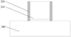
参照图6,提供半导体衬底200,在所述半导体衬底的表面形成栅极结构210。6, a
其中,所述半导体衬底200可以为硅衬底,或者所述半导体衬底200的材料还可以包括锗、锗化硅、碳化硅、砷化镓或镓化铟,所述半导体衬底200还可以为绝缘体上的硅衬底或者绝缘体上的锗衬底。Wherein, the
所述栅极结构210可以包括栅介质层、栅极材料层和栅硬掩模材料等常规结构,所述栅介质层可以位于所述半导体衬底的表面,所述栅极材料层可以位于所述栅介质层的表面。The
进一步地,在所述半导体衬底200的表面形成栅极结构210的步骤可以包括:形成侧墙220,所述侧墙220位于所述栅极结构210的两侧;其中,后续形成的所述第一介质层231以及所述第二介质层240可以位于所述侧墙220的两侧。Further, the step of forming the
具体地,所述栅极结构210还可以包括侧墙220,所述侧墙220位于所述栅极结构210的两侧,用于对所述栅极结构210的内部结构进行保护。Specifically, the
进一步地,所述栅极材料可以采用多晶硅材料,还可以采用高K值金属栅材料,以满足多种半导体器件的需要。Further, the gate material can be a polysilicon material or a high-K-value metal gate material to meet the needs of various semiconductor devices.
参照图7,形成初始第一介质层230,所述初始第一介质层230位于所述栅极结构210的两侧。Referring to FIG. 7 , an initial first
参照图8,对所述初始第一介质层230进行刻蚀,以形成所述第一介质层231,且所述第一介质层231的顶部表面低于所述栅极结构210的顶部表面。8 , the initial first
进一步地,所述第一介质层231的材料可以选自:氮碳化硅(SiCN)、氧化硅以及氮化硅。Further, the material of the
需要指出的是,所述第一介质层231可以为单种材料,例如上述三种材料中的一种;所述第一介质层231还可以为多种材料堆叠而成的材料,例如可以为氧化硅以及氮化硅的堆叠层,以减轻对晶圆的应力。It should be noted that the
其中,所述氧化硅例如可以为SiO2,所述氮化硅例如可以为Si3N4。Wherein, the silicon oxide can be, for example, SiO2 , and the silicon nitride can be, for example, Si3 N4 .
进一步地,形成第一介质层231的步骤可以包括:形成初始第一介质层230,所述初始第一介质层230覆盖所述栅极结构110;对所述初始第一介质层230进行平坦化;对所述初始第一介质层230进行刻蚀,以形成所述第一介质层231。Further, the step of forming the
更进一步地,所述第一介质层231的顶部表面可以与所述栅极结构210的顶部表面齐平,从而可以采用所述栅极结构(包含侧墙)210的顶部表面作为平坦化工艺的停止层,有助于降低工艺复杂度。Further, the top surface of the
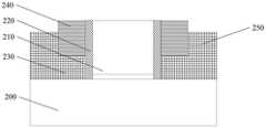
参照图9,形成第二介质层240,所述第二介质层240位于所述第一介质层231的表面以及位于所述栅极结构210的两侧。Referring to FIG. 9 , a
如图所示,所述第二介质层240可以位于所述栅极结构210的顶部两侧,具体地,可以位于所述栅极结构210的上半部分的两侧;第一介质层231可以位于所述栅极结构210的底部两侧,具体地,可以位于所述栅极结构210的下半部分的两侧。其中,所述栅极结构210的上半部分与下半部分之间的比例可以根据具体需要进行设置,此处不做限制。As shown in the figure, the
具体地,所述第二介质层240的宽度小于所述第一介质层231的宽度,从而可以在后续形成源漏外延区后,使得源漏外延区的宽度小于第一介质层231的宽度,也即实现源漏外延区的台阶形状。Specifically, the width of the
其中,所述宽度的方向平行于所述半导体器件的沟道方向。Wherein, the direction of the width is parallel to the channel direction of the semiconductor device.
进一步地,所述第二介质层240的材料可以选自:氧化硅以及氮化硅。Further, the material of the
需要指出的是,所述第二介质层240可以为单种材料,例如上述两种材料中的一种;所述第二介质层240还可以为多种材料堆叠而成的材料,例如可以为氧化硅以及氮化硅的堆叠层,以减轻对晶圆的应力。It should be noted that the
更进一步地,所述第一介质层231的材料不同于所述第二介质层240的材料。Further, the material of the
在一种非限制性的实施例中,可以设置所述第一介质层231的材料为氧化硅,设置第二介质层240的材料为SiCN。In a non-limiting embodiment, the material of the
在本发明实施例中,通过设置所述第一介质层231的材料不同于所述第二介质层240的材料,有助于在形成第二介质层240之后,刻蚀位于所述第二介质层240下方的第一介质层231时,避免对需要保留的第二介质层240产生伤害。In the embodiment of the present invention, by setting the material of the
更进一步地,所述第一介质层231与所述第二介质层240的刻蚀比可以大于预设阈值。Furthermore, the etching ratio of the
在本发明实施例中,通过设置所述第一介质层231与所述第二介质层240的刻蚀比大于预设阈值,可以在形成第二介质层240之后,刻蚀位于所述第二介质层240下方的第一介质层231时,对需要保留的第二介质层240进行有效保护。In the embodiment of the present invention, by setting the etching ratio of the
进一步地,形成第二介质层240的步骤可以包括:形成初始第二介质层(图未示),所述初始第二介质层覆盖所述栅极结构以及所述第一介质层231;对所述初始第二介质层进行平坦化;对所述初始第二介质层进行刻蚀,以形成所述第二介质层240。Further, the step of forming the
更进一步地,所述第二介质层240的顶部表面与所述栅极结构210的顶部表面齐平。Furthermore, the top surface of the
在本发明实施例中,通过设置所述第二介质层240的顶部表面与所述栅极结构210的顶部表面齐平,从而可以采用所述栅极结构(包含侧墙)210的顶部表面作为平坦化工艺的停止层,有助于降低工艺复杂度。In the embodiment of the present invention, by setting the top surface of the
需要指出的是,在本申请实施例中,还可以不采用平坦化的步骤,例如可以采用自对准刻蚀工艺实现。It should be pointed out that, in the embodiments of the present application, the step of planarization may not be adopted, for example, a self-aligned etching process may be adopted.
参照图10,去除所第一介质层231,以暴露出所述第二介质层240下方的栅极结构210的侧壁表面。Referring to FIG. 10 , the
可以理解的是,所述第二介质层240下方的栅极结构210的侧壁表面可以为所述栅极结构210的侧墙220的侧壁表面。It can be understood that, the sidewall surface of the
参照图11,形成源漏外延区250,所述源漏外延区250位于所述第二介质层240的两侧以及所述第二介质层240下方的栅极结构210的两侧。Referring to FIG. 11 , source-drain
具体地,可以采用外延生长的方式,形成源漏外延区,即所述源漏外延区250。由于所述源漏外延区250是一体化形成的,工艺复杂度和生产成本较低。Specifically, the source-drain epitaxial region, that is, the source-
需要指出的是,由于在现有技术中,生长第二源漏外延区之前,还需要采用回刻(Etch-back)工艺和清洗(Clean)工艺对第一源漏外延区进行表面处理,因此会对第一源漏外延区产生一定厚度的损伤。也即在本申请实施例中,生长更薄的源漏外延区即可得到现有技术中的源漏外延区厚度,进一步降低了生成成本。It should be pointed out that, because in the prior art, before growing the second source-drain epitaxial region, the surface treatment of the first source-drain epitaxial region needs to be performed by an etch-back (Etch-back) process and a cleaning (Clean) process. The first source-drain epitaxial region will be damaged with a certain thickness. That is, in the embodiment of the present application, the source-drain epitaxial region thickness in the prior art can be obtained by growing a thinner source-drain epitaxial region, which further reduces the production cost.
进一步地,所述源漏外延区250的顶部表面可以低于所述栅极结构210的顶部表面。Further, the top surface of the source-
在本发明实施例中,通过设置所述源漏外延区250的顶部表面可以低于所述栅极结构210的顶部表面,从而可以根据具体需求生长适当高度的源漏外延区,降低生产成本。In the embodiment of the present invention, by setting the top surface of the source-
在本发明实施例中,通过先形成第一介质层231作为牺牲层,可以在需要形成源漏外延区的区域先形成第一介质层231,从而在去除第一介质层231后,仅需要单次外延生长工艺即可形成具有台阶形状的源漏外延区,相比于现有技术中,需要两次外延生长工艺才能形成具有台阶形状的源漏外延区,采用本发明实施例的方案,可以有效降低工艺复杂度和生产成本,提高生产稳定性和器件性能。进一步地,本发明实施例中的技术方案,与现有技术中的生产工艺完全兼容,无需引入额外的机台及耗材,无制造污染的风险。In the embodiment of the present invention, by first forming the
在本申请实施例中,还公开了一种半导体器件,结合参照图9和图11,包括:半导体衬底200;栅极结构210,位于所述半导体衬底200的表面;第二介质层240,位于所述栅极结构210的顶部两侧;源漏外延区250,位于所述第二介质层240的两侧以及所述第二介质层240下方的栅极结构210的两侧;其中,所述源漏外延区250是在去除第一介质层231,以暴露出所述第二介质层240下方的栅极结构的侧壁表面之后形成的;所述第一介质层231是在形成第二介质层240之前形成的,所述第一介质层231位于所述栅极结构210的两侧,且所述第一介质层231的顶部表面低于所述栅极结构的顶部表面;所述第二介质层240位于所述第一介质层的表面且所述第二介质层240的宽度小于所述第一介质层231的宽度。In the embodiment of the present application, a semiconductor device is also disclosed, referring to FIG. 9 and FIG. 11 , including: a
进一步地,所述第二介质层240的顶部表面可以与所述栅极结构210的顶部表面齐平。Further, the top surface of the
进一步地,所述源漏外延区250的顶部表面可以低于所述栅极结构210的顶部表面。Further, the top surface of the source-
关于该半导体器件的原理、具体实现和有益效果请参照前文描述的关于半导体器件的形成方法的相关描述,此处不再赘述。For the principle, specific implementation and beneficial effects of the semiconductor device, please refer to the related description about the formation method of the semiconductor device described above, which will not be repeated here.
虽然本发明披露如上,但本发明并非限定于此。任何本领域技术人员,在不脱离本发明的精神和范围内,均可作各种更动与修改,因此本发明的保护范围应当以权利要求所限定的范围为准。Although the present invention is disclosed above, the present invention is not limited thereto. Any person skilled in the art can make various changes and modifications without departing from the spirit and scope of the present invention. Therefore, the protection scope of the present invention should be based on the scope defined by the claims.
Claims (10)
Translated fromChinesePriority Applications (1)
| Application Number | Priority Date | Filing Date | Title |
|---|---|---|---|
| CN202011432877.XACN112582476B (en) | 2020-12-09 | 2020-12-09 | Semiconductor device and method of forming the same |
Applications Claiming Priority (1)
| Application Number | Priority Date | Filing Date | Title |
|---|---|---|---|
| CN202011432877.XACN112582476B (en) | 2020-12-09 | 2020-12-09 | Semiconductor device and method of forming the same |
Publications (2)
| Publication Number | Publication Date |
|---|---|
| CN112582476A CN112582476A (en) | 2021-03-30 |
| CN112582476Btrue CN112582476B (en) | 2022-05-06 |
Family
ID=75130583
Family Applications (1)
| Application Number | Title | Priority Date | Filing Date |
|---|---|---|---|
| CN202011432877.XAActiveCN112582476B (en) | 2020-12-09 | 2020-12-09 | Semiconductor device and method of forming the same |
Country Status (1)
| Country | Link |
|---|---|
| CN (1) | CN112582476B (en) |
Citations (2)
| Publication number | Priority date | Publication date | Assignee | Title |
|---|---|---|---|---|
| US5710054A (en)* | 1996-08-26 | 1998-01-20 | Advanced Micro Devices, Inc. | Method of forming a shallow junction by diffusion from a silicon-based spacer |
| JP2002231942A (en)* | 2000-11-28 | 2002-08-16 | Toshiba Corp | Semiconductor device and manufacturing method thereof |
Family Cites Families (10)
| Publication number | Priority date | Publication date | Assignee | Title |
|---|---|---|---|---|
| US6812103B2 (en)* | 2002-06-20 | 2004-11-02 | Micron Technology, Inc. | Methods of fabricating a dielectric plug in MOSFETS to suppress short-channel effects |
| US6909186B2 (en)* | 2003-05-01 | 2005-06-21 | International Business Machines Corporation | High performance FET devices and methods therefor |
| US7060576B2 (en)* | 2003-10-24 | 2006-06-13 | Intel Corporation | Epitaxially deposited source/drain |
| US7749850B2 (en)* | 2007-11-07 | 2010-07-06 | Semiconductor Energy Laboratory Co., Ltd. | Method for manufacturing semiconductor device |
| US9076817B2 (en)* | 2011-08-04 | 2015-07-07 | International Business Machines Corporation | Epitaxial extension CMOS transistor |
| US8497180B2 (en)* | 2011-08-05 | 2013-07-30 | Globalfoundries Inc. | Transistor with boot shaped source/drain regions |
| EP2696369B1 (en)* | 2012-08-10 | 2021-01-13 | IMEC vzw | Methods for manufacturing a field-effect semiconductor device |
| CN106328707A (en)* | 2015-07-06 | 2017-01-11 | 中芯国际集成电路制造(上海)有限公司 | Transistor and manufacturing method |
| US11049939B2 (en)* | 2015-08-03 | 2021-06-29 | Semiwise Limited | Reduced local threshold voltage variation MOSFET using multiple layers of epi for improved device operation |
| US20190051565A1 (en)* | 2017-08-10 | 2019-02-14 | Globalfoundries Inc. | Cmos devices and manufacturing method thereof |
- 2020
- 2020-12-09CNCN202011432877.XApatent/CN112582476B/enactiveActive
Patent Citations (2)
| Publication number | Priority date | Publication date | Assignee | Title |
|---|---|---|---|---|
| US5710054A (en)* | 1996-08-26 | 1998-01-20 | Advanced Micro Devices, Inc. | Method of forming a shallow junction by diffusion from a silicon-based spacer |
| JP2002231942A (en)* | 2000-11-28 | 2002-08-16 | Toshiba Corp | Semiconductor device and manufacturing method thereof |
Also Published As
| Publication number | Publication date |
|---|---|
| CN112582476A (en) | 2021-03-30 |
Similar Documents
| Publication | Publication Date | Title |
|---|---|---|
| CN104795332A (en) | Fin-type field effect transistor forming method | |
| CN105448917A (en) | Semiconductor structure and method of forming same | |
| CN104103516A (en) | Shallow groove isolation structure and formation method thereof | |
| CN107564859A (en) | Semiconductor device and its manufacture method | |
| CN106298929B (en) | The forming method of fin field effect pipe | |
| CN106558556A (en) | The forming method of fin field effect pipe | |
| CN104347409B (en) | The forming method of semiconductor structure | |
| CN111769046B (en) | Semiconductor structures and methods of forming them | |
| CN105097525A (en) | Formation method of semiconductor device | |
| CN109950311B (en) | Semiconductor structure and forming method thereof | |
| WO2023108784A1 (en) | Semiconductor device and method for manufacturing same | |
| CN111384172B (en) | Semiconductor devices and methods of forming the same | |
| CN112582476B (en) | Semiconductor device and method of forming the same | |
| CN103632978B (en) | The forming method of semiconductor structure | |
| CN112652578B (en) | Method of forming semiconductor structure, transistor | |
| CN111446286B (en) | Semiconductor structures and methods of forming them | |
| CN114792728A (en) | Semiconductor structure and forming method thereof | |
| CN114792730A (en) | Semiconductor structure and forming method thereof | |
| CN114497035A (en) | Semiconductor structure and method for forming semiconductor structure | |
| CN107045983B (en) | Transistor and method of forming the same | |
| CN110797261B (en) | Semiconductor structure and forming method thereof | |
| CN113451208B (en) | Semiconductor structures and methods of forming them | |
| CN110299286B (en) | Method for manufacturing epitaxial fin-shaped structure | |
| CN115223872A (en) | Semiconductor structure and method of forming the same | |
| CN118824855A (en) | Method for forming semiconductor structure |
Legal Events
| Date | Code | Title | Description |
|---|---|---|---|
| PB01 | Publication | ||
| PB01 | Publication | ||
| SE01 | Entry into force of request for substantive examination | ||
| SE01 | Entry into force of request for substantive examination | ||
| GR01 | Patent grant | ||
| GR01 | Patent grant |